WO2017033642A1 - 半導体装置、半導体集積回路、及び負荷駆動装置 - Google Patents
半導体装置、半導体集積回路、及び負荷駆動装置 Download PDFInfo
- Publication number
- WO2017033642A1 WO2017033642A1 PCT/JP2016/071658 JP2016071658W WO2017033642A1 WO 2017033642 A1 WO2017033642 A1 WO 2017033642A1 JP 2016071658 W JP2016071658 W JP 2016071658W WO 2017033642 A1 WO2017033642 A1 WO 2017033642A1
- Authority
- WO
- WIPO (PCT)
- Prior art keywords
- wiring layer
- semiconductor device
- metal wiring
- layer
- interlayer connection
- Prior art date
- Legal status (The legal status is an assumption and is not a legal conclusion. Google has not performed a legal analysis and makes no representation as to the accuracy of the status listed.)
- Ceased
Links
Images


Classifications
-
- H—ELECTRICITY
- H10—SEMICONDUCTOR DEVICES; ELECTRIC SOLID-STATE DEVICES NOT OTHERWISE PROVIDED FOR
- H10W—GENERIC PACKAGES, INTERCONNECTIONS, CONNECTORS OR OTHER CONSTRUCTIONAL DETAILS OF DEVICES COVERED BY CLASS H10
- H10W20/00—Interconnections in chips, wafers or substrates
- H10W20/40—Interconnections external to wafers or substrates, e.g. back-end-of-line [BEOL] metallisations or vias connecting to gate electrodes
- H10W20/498—Resistive arrangements or effects of, or between, wiring layers
-
- H—ELECTRICITY
- H10—SEMICONDUCTOR DEVICES; ELECTRIC SOLID-STATE DEVICES NOT OTHERWISE PROVIDED FOR
- H10D—INORGANIC ELECTRIC SEMICONDUCTOR DEVICES
- H10D30/00—Field-effect transistors [FET]
- H10D30/60—Insulated-gate field-effect transistors [IGFET]
-
- H—ELECTRICITY
- H10—SEMICONDUCTOR DEVICES; ELECTRIC SOLID-STATE DEVICES NOT OTHERWISE PROVIDED FOR
- H10D—INORGANIC ELECTRIC SEMICONDUCTOR DEVICES
- H10D64/00—Electrodes of devices having potential barriers
- H10D64/01—Manufacture or treatment
- H10D64/011—Manufacture or treatment of electrodes ohmically coupled to a semiconductor
-
- H—ELECTRICITY
- H10—SEMICONDUCTOR DEVICES; ELECTRIC SOLID-STATE DEVICES NOT OTHERWISE PROVIDED FOR
- H10D—INORGANIC ELECTRIC SEMICONDUCTOR DEVICES
- H10D84/00—Integrated devices formed in or on semiconductor substrates that comprise only semiconducting layers, e.g. on Si wafers or on GaAs-on-Si wafers
- H10D84/80—Integrated devices formed in or on semiconductor substrates that comprise only semiconducting layers, e.g. on Si wafers or on GaAs-on-Si wafers characterised by the integration of at least one component covered by groups H10D12/00 or H10D30/00, e.g. integration of IGFETs
- H10D84/82—Integrated devices formed in or on semiconductor substrates that comprise only semiconducting layers, e.g. on Si wafers or on GaAs-on-Si wafers characterised by the integration of at least one component covered by groups H10D12/00 or H10D30/00, e.g. integration of IGFETs of only field-effect components
- H10D84/83—Integrated devices formed in or on semiconductor substrates that comprise only semiconducting layers, e.g. on Si wafers or on GaAs-on-Si wafers characterised by the integration of at least one component covered by groups H10D12/00 or H10D30/00, e.g. integration of IGFETs of only field-effect components of only insulated-gate FETs [IGFET]
-
- H—ELECTRICITY
- H10—SEMICONDUCTOR DEVICES; ELECTRIC SOLID-STATE DEVICES NOT OTHERWISE PROVIDED FOR
- H10P—GENERIC PROCESSES OR APPARATUS FOR THE MANUFACTURE OR TREATMENT OF DEVICES COVERED BY CLASS H10
- H10P14/00—Formation of materials, e.g. in the shape of layers or pillars
- H10P14/40—Formation of materials, e.g. in the shape of layers or pillars of conductive or resistive materials
-
- H—ELECTRICITY
- H10—SEMICONDUCTOR DEVICES; ELECTRIC SOLID-STATE DEVICES NOT OTHERWISE PROVIDED FOR
- H10W—GENERIC PACKAGES, INTERCONNECTIONS, CONNECTORS OR OTHER CONSTRUCTIONAL DETAILS OF DEVICES COVERED BY CLASS H10
- H10W20/00—Interconnections in chips, wafers or substrates
- H10W20/01—Manufacture or treatment
-
- H—ELECTRICITY
- H10—SEMICONDUCTOR DEVICES; ELECTRIC SOLID-STATE DEVICES NOT OTHERWISE PROVIDED FOR
- H10W—GENERIC PACKAGES, INTERCONNECTIONS, CONNECTORS OR OTHER CONSTRUCTIONAL DETAILS OF DEVICES COVERED BY CLASS H10
- H10W20/00—Interconnections in chips, wafers or substrates
- H10W20/40—Interconnections external to wafers or substrates, e.g. back-end-of-line [BEOL] metallisations or vias connecting to gate electrodes
- H10W20/41—Interconnections external to wafers or substrates, e.g. back-end-of-line [BEOL] metallisations or vias connecting to gate electrodes characterised by their conductive parts
- H10W20/42—Vias, e.g. via plugs
-
- H—ELECTRICITY
- H01—ELECTRIC ELEMENTS
- H01F—MAGNETS; INDUCTANCES; TRANSFORMERS; SELECTION OF MATERIALS FOR THEIR MAGNETIC PROPERTIES
- H01F7/00—Magnets
- H01F7/06—Electromagnets; Actuators including electromagnets
- H01F7/064—Circuit arrangements for actuating electromagnets
-
- H—ELECTRICITY
- H10—SEMICONDUCTOR DEVICES; ELECTRIC SOLID-STATE DEVICES NOT OTHERWISE PROVIDED FOR
- H10D—INORGANIC ELECTRIC SEMICONDUCTOR DEVICES
- H10D62/00—Semiconductor bodies, or regions thereof, of devices having potential barriers
- H10D62/10—Shapes, relative sizes or dispositions of the regions of the semiconductor bodies; Shapes of the semiconductor bodies
- H10D62/124—Shapes, relative sizes or dispositions of the regions of semiconductor bodies or of junctions between the regions
- H10D62/126—Top-view geometrical layouts of the regions or the junctions
Definitions
- the present invention relates to a semiconductor device, a semiconductor integrated circuit, and a load driving device.
- a load driving device that drives a load is widely used.
- This load driving device controls ON / OFF of a switching element, and a large current flows through a transistor used as the switching element.
- the transistors are integrated circuits, and a large number of transistors are closely arranged, the drains of the individual transistors are commonly connected to the drain pads, and the sources of the individual transistors are commonly connected to the source pads. ing.
- Patent Document 1 for the purpose of making the current density uniform.
- the semiconductor device described in Patent Document 1 has a drain through hole that connects the drain terminal of each transistor and the first conductor layer. Furthermore, a source through-hole connecting the source terminal of each transistor and the second conductor layer is provided. The arrangement distribution of the source through holes and the drain through holes is changed according to the distance from the source pad and the drain pad.
- the current density increases in a region near the boundary where the first conductor layer and the second conductor layer face each other, and the entire region of the transistor arranged in two dimensions is arranged.
- the current density cannot be made uniform.
- a semiconductor device includes a transistor layer in which a plurality of transistors each having an input unit, an output unit, and a control unit are arranged two-dimensionally, and is connected to an input terminal and an output terminal.
- a plurality of wiring layers for electrically connecting to the input terminal and electrically connecting the output section to the output terminal, and a plurality of interlayer connection conductor groups for connecting the plurality of wiring layers and the transistor layers, respectively.
- the plurality of wiring layers includes a first wiring in which at least one input-side wiring layer connected to the input terminal and at least one output-side wiring layer connected to the output terminal are arranged along a predetermined arrangement direction.
- the resistance values of the plurality of interlayer connection conductor groups having layers differ from each other depending on the position in the arrangement direction.
- the current density of the transistors arranged in two dimensions can be made uniform.
- FIG. 2 is a cross-sectional view taken along the line A-A ′ of the semiconductor device of FIG. 1.
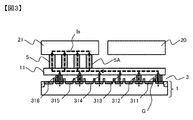
- FIG. 2 is a cross-sectional view taken along the line B-B ′ of the semiconductor device of FIG. 1. It is an equivalent circuit of a metal wiring layer and a through hole.
- FIG. 6 is a cross-sectional view taken along line E-E ′ of the semiconductor device of FIG. 5.
- FIG. 6 is a cross-sectional view taken along the line F-F ′ of the semiconductor device of FIG. 5. It is a top view of the semiconductor device in a 2nd embodiment.
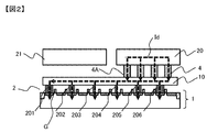
- the plurality of metal wiring layers 10 are connected to the drain electrodes D of the plurality of transistors of the transistor layer 1 through the through hole group 2 which is an interlayer connection conductor constituted by the plurality of through holes.
- the plurality of metal wiring layers 11 are connected to the source electrodes S of the plurality of transistors of the transistor layer 1 through the through-hole group 3 which is an interlayer connection conductor constituted by the plurality of through-holes.
- each through hole constituting each of the through hole groups 2 and 3 is indicated by a square.
- a metal wiring layer 20 and a metal wiring layer 21 which are second wiring layers are provided on the metal wiring layer 10 and the metal wiring layer 11.
- the metal wiring layer 20 is connected to the first metal wiring layer 10 through a plurality of through holes 4 which are interlayer connection conductors.
- the metal wiring layer 21 is connected to the first metal wiring layer 11 through a plurality of through holes 5 which are interlayer connection conductors.
- the through holes 4 and 5 are indicated by ⁇ symbols.
- the metal wiring layer 20 is provided with an input terminal pad 7 for injecting a drain current, and is connected to the input terminal of the semiconductor device through the input terminal pad 7.
- the metal wiring layer 21 is provided with an output terminal pad 8 for extracting a source current, and is connected to the output terminal of the semiconductor device via the output terminal pad 8. As described above, the second wiring layer is divided into two parts, the drain metal wiring layer 20 and the source metal wiring layer 21.
- the metal wiring layers 20 and 21 extend in the Y direction shown in FIG. 1, and the metal wiring layers 10 and 11 extend in the X direction. These wiring layers are arranged so as to cover the entire transistor layer 1 in which the transistors are arranged two-dimensionally.
- the metal wiring layer 20 and the metal wiring layer 21 are arranged along this arrangement direction with the X direction as the arrangement direction.
- a current path Id flowing from the input terminal pad 7 (see FIG. 1) to the transistor layer 1 passes through the metal wiring layer 20, passes through the plurality of through holes 4, and flows into the first metal wiring layer 10. Further, it flows from the metal wiring layer 10 to each drain electrode of the transistor layer 1 through the plurality of through-hole groups 201 to 206.
- the plurality of through-hole groups 201 to 206 are arranged in the metal wiring layer 10 at equal intervals.
- the transistor below the through hole 4 among the plurality of transistors arranged in the transistor layer 1 has a short current path through the metal wiring layer 10.
- a transistor far from the through hole 4 has a long current path through the metal wiring layer 10. Since the voltage drop due to the wiring resistance when a current flows through the metal wiring layer 10 is larger as the path through the metal wiring layer 10 is longer, the potential of the upper surfaces of the through-hole groups 201 to 203 is the lowest in the through-hole group 201. , 203 in order.
- the through-hole groups 204, 205, and 206 are all directly below the through-hole 4 that connects the metal wiring layer 20 and the metal wiring layer 10, the potentials on the upper surfaces of these through-hole groups 204, 205, and 206 are approximately the same. It is.
- a current path Is flowing from the transistor layer 1 to the output terminal pad 8 flows from each source electrode of the transistor layer 1 to the metal wiring layer 11 through the plurality of through-hole groups 311 to 316. . Furthermore, it flows from the metal wiring layer 11 through the plurality of through holes 5 to the output terminal pad 8 (see FIG. 1) through the metal wiring layer 21.
- the plurality of through-hole groups 3311 to 316 are arranged in the metal wiring layer 11 at equal intervals.
- the potential difference between the upper surfaces of the through-hole groups 201 to 206 connected to the drain electrode D and the upper surfaces of the through-hole groups 311 to 316 connected to the source electrode S on the opposite side across the gate electrode is compared. Specifically, the potential difference between the through-hole group 201 shown in FIGS. 1 and 2 and the through-hole group 316 shown in FIGS. 1 and 3 is compared. Similarly, the potential difference between the through hole group 202 shown in FIGS. 1 and 2 and the through hole group 315 shown in FIGS. 1 and 3 is compared. The potential difference between the through-hole group 203 shown in FIGS. 1 and 2 and the through-hole group 314 shown in FIGS. 1 and 3 is compared.
- the potential difference between the through hole group 204 shown in FIGS. 1 and 2 and the through hole group 313 shown in FIGS. 1 and 3 will be compared.
- the potential difference between the through-hole group 205 shown in FIGS. 1 and 2 and the through-hole group 312 shown in FIGS. 1 and 3 will be compared.
- the potential difference between the through-hole group 206 shown in FIGS. 1 and 2 and the through-hole group 311 shown in FIGS. 1 and 3 will be compared.
- the potential difference between the through hole group 201 located farthest from the leftmost through hole 4A shown in FIG. 2 and the corresponding through hole group 316 is the smallest.
- the potential difference between the through hole group 311 located farthest from the rightmost through hole 5A shown in FIG. 3 and the corresponding through hole group 206 is the smallest.
- the potential difference between the through hole group 203 located closest to the through hole 4A shown in FIG. 2 and the corresponding through hole group 314 is the largest.
- the potential difference between the through hole group 313 located closest to the through hole 5A shown in FIG. 3 and the corresponding through hole group 204 is the largest.
- the potential difference between the upper surfaces of the other through-hole groups is an intermediate value thereof.
- the distribution density of through-holes in these through-hole groups is increased so that is lower than other through-hole groups.
- the other through-hole groups 202 to 205 and 312 to 315 have low through-hole distribution density in these through-hole groups so as to increase the resistance value.
- the potential difference between the drain electrode D and the source electrode S adjacent to each other is different from the potential difference between the bottom surface of the through hole group 201 and the bottom surface of the through hole group 316, and the through hole.
- This is equivalent to the potential difference between the bottom surface of the group 206 and the bottom surface of the through-hole group 311. That is, in the present embodiment, the metal wiring layers 10 and 11 and the metal wiring layers 20 and 21 are connected so that the potential difference between the drain electrode D and the source electrode S sandwiching the gate electrode G is equal in each transistor.
- the resistance values of the through hole groups 201 to 206 and 311 to 316 are changed.
- the wiring resistance of the metal wiring layers 20 and 21 is lower than that of the metal wiring layers 10 and 11.
- the right half wiring resistance 101 of the metal wiring layer 10 and the left half wiring resistance 111 of the metal wiring layer 11 are connected to the metal wiring layers 20 and 21 through the through holes 4 and 5.
- the voltage drop due to these wiring resistances is small.
- the voltage drop due to the wiring resistance 102 in the left half of the metal wiring layer 10 and the wiring resistance 112 in the right half of the metal wiring layer 11 is the surface of the drain-source voltage of each transistor disposed in the large-area transistor layer 1. Generate internal distribution. Therefore, when the voltage drop due to these wiring resistances is not uniform, it causes nonuniform distribution of the current density in the transistor layer 1.
- FIG. 5 is a plan view of the semiconductor device when the resistance values of the through-hole groups 2 and 3 are made uniform on the transistor layer 1 without changing the resistance values.
- the same parts as those in FIG. 1 are denoted by the same reference numerals, and the description thereof is omitted.
- 6 is a cross-sectional view taken along the line E-E ′ of FIG. 5, and is a cross-sectional view taken along one of the plurality of metal wiring layers 10. 5 and 6, the through-hole groups 2 that are commonly shown in these drawings are shown as through-hole groups 621 to 626.
- a current path Is ′ flowing from the transistor layer 1 to the output terminal pad 8 passes from each source electrode of the transistor layer 1 to the metal wiring layer 11 through a plurality of through-hole groups 631 to 636. Flowing. Further, it flows from the metal wiring layer 11 through the plurality of through holes 5 to the output terminal pad 8 (see FIG. 5) through the metal wiring layer 21. Similarly to the current path Id ', the current flowing through the current path Is' increases as the wiring length of the metal wiring layer 11 between the through hole 5A increases and the voltage drop due to the wiring resistance increases, resulting in a low current.
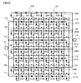
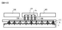
- FIG. 8 is a plan view of the semiconductor device according to the second embodiment.
- the second wiring layer is divided into three metal wiring layers 20, 21, and 22 and arranged in parallel.
- the metal wiring layers 20 and 22 are provided with input terminal pads 7, respectively. Yes.
- the metal wiring layer 21 is provided with output terminal pads 8.
- the metal wiring layer 21 on the source side is sandwiched between the metal wiring layers 20 and 22 on the drain side from both sides. Further, the first metal wiring layer 10 and the metal wiring layer 11 are disposed so as to intersect with the second metal wiring layers 20, 21, and 22.
- FIG. 9 is a cross-sectional view taken along the line J-J ′ of the semiconductor device of FIG. 8, and FIG. 10 is a cross-sectional view taken along the line K-K ′ of the semiconductor device of FIG.
- the metal wiring layer 10 includes a plurality of drain electrodes that are input portions of a plurality of transistors in the transistor layer 1 through a through hole group 2 that is an interlayer connection conductor constituted by a plurality of through holes. Connected to D.
- the metal wiring layer 11 includes a plurality of source electrodes that are output portions of a plurality of transistors in the transistor layer 1 through a through hole group 3 that is an interlayer connection conductor constituted by a plurality of through holes. S is connected.
- the second wiring layer in the upper layer is divided into more metal wiring layers 20, 21, and 22 as compared with the first embodiment.
- These wiring layers connected to different types of electrodes are alternately arranged along the arrangement direction (vertical direction in FIG. 8).
- the wiring length between the through hole group 2 and the through hole group 3 is shortened, so that the wiring resistance of the first metal wiring layers 10 and 11 is reduced.
- the voltage drop due to can be reduced.
- the wiring between each through-hole group 2 and the through-hole group 3 is connected between these through the through-hole groups 2 and 3. The current of each transistor in the transistor layer 1 flows.
- the current density of the metal wiring layers 10 and 11 near the through holes 4 and 5 is increased.
- the wiring length of the metal wiring layers 10 and 11 between the through hole 4 and the through hole 5 is short, the current density can be reduced.
- the current Id flowing from the drain side metal wiring layers 20 and 22 to the transistor layer 1 flows through the through hole 4, flows through the metal wiring layer 10, and flows from the through hole group 2 to the transistor layer 1.
- the potential on the upper surface of the through-hole group 2 becomes lower as the distance from the through-hole 4A on the drain side is closer to the central portion of the metal wiring layer 10 due to a voltage drop due to the wiring resistance of the metal wiring layer 10. Therefore, in the metal wiring layer 21 on the source side, the distribution density of the through-hole group 2 is increased as it is closer to the center line C orthogonal to the arrangement direction of the metal wiring layers 20, 21, 22 (vertical direction in FIG. 8). The closer to the through holes 4A connected to the drain side metal wiring layers 20 and 22, the lower the distribution density of the through hole group 2, and the resistance value is adjusted.
- the through hole is formed in the same manner.
- the current density of the transistor layer 1 can be made uniform.
- the density is decreased, and the distribution density of the through holes constituting the through hole groups 2 and 3 is increased as the distance from the position is increased.
- the distribution density of the through holes constituting the through hole groups 4 and 5 is lowered.
- the distribution density of the through holes constituting the groups 4 and 5 is increased.
- the example in which the metal wiring layer has two layers or three layers has been described. However, even if the metal wiring layer has four or more layers, the same can be implemented. Further, the number and shape of the through holes arranged in each metal wiring layer are schematically shown for easy understanding of the embodiment, and are not limited to the above-described embodiment.
- the input terminal of the switching element 92 is connected to the power source VB.
- a load 94 is connected to the output terminal of the switching element 92.
- a gate drive circuit 93 is connected to the control terminal of the switching element 92.
- the output current of the switching element 92 is controlled on and off, and the current to the load 94 is controlled.
- the metal wiring layer has a locally high current density. Therefore, the area of the semiconductor device can be reduced accordingly.
- a transistor that flows a large current such as a switching element 92 that drives a load such as an in-vehicle electromagnetic actuator, requires a size of several hundred micrometers or more, and occupies a large area in a semiconductor device.
- the semiconductor device described in the first to third embodiments as a switching element, the area of the semiconductor device can be reduced and the chip cost of the semiconductor device can be reduced.
- a semiconductor device inputs a transistor layer 1 in which a plurality of transistors each having a drain electrode D, a source electrode S, and a gate electrode G are two-dimensionally arranged, and a drain electrode D of the plurality of transistors in the transistor layer 1
- the plurality of wiring layers are a second wiring layer, a metal wiring layer 20 that is an input side wiring layer connected to the input terminal via the input terminal pad 7, and an output terminal via the output terminal pad 8.
- the metal wiring layer 21 that is the output-side wiring layer connected to the wiring layer has a wiring layer arranged along a predetermined arrangement direction.
- the resistance values of the plurality of interlayer connection conductors differ from each other depending on the positions of the metal wiring layers 20 and 21 in the arrangement direction.
- the plurality of wiring layers are provided on the transistor layer 1 side with respect to the second wiring layer including the metal wiring layers 20 and 21 and have a plurality of metal wiring layers 10 and 11. And a first wiring layer.
- the plurality of interlayer connection conductors have a plurality of through-hole groups 2 and 3 that connect the metal wiring layers 10 and 11 and the drain electrodes D and source electrodes S of the plurality of transistors in the transistor layer 1.
- the resistance values of the plurality of through-hole groups 2 and 3 are different from each other depending on the positions of the metal wiring layers 20 and 21 in the arrangement direction. As a result, the current density of the transistors arranged in two dimensions can be made uniform.
- the resistance values of the plurality of through-hole groups 2 and 3 change based on at least the wiring length of the metal wiring layers 10 and 11. Thereby, the wiring resistance according to the wiring length can be adjusted by the resistance values of the through-hole groups 2 and 3.
- the plurality of interlayer connection conductors have a plurality of through-hole groups 2 and 3 and through-holes 4 and 5 that connect the metal wiring layers 20 and 21 and the metal wiring layers 10 and 11.
- the wiring lengths of the metal wiring layers 10 and 11 start from the positions of the through holes 4 and 5. Thereby, each resistance value of the through-hole groups 2 and 3 can be adjusted based on the positions of the through-holes 4 and 5.
- the resistance values of the through-hole groups 2 and 3 are higher as they are closer to the boundary between the metal wiring layer 20 that is the input-side wiring layer and the metal wiring layer 21 that is the output-side wiring layer. Thereby, the potential difference between the upper surfaces of the through-hole groups 2 and 3 can be made uniform regardless of the position on the transistor.
- the first wiring layer includes two metal wiring layers 20 and 22 that are input-side wiring layers and one metal wiring layer 21 that is an output-side wiring layer. 8 are arranged alternately along the arrangement direction shown in the vertical direction.
- the resistance value of the through-hole groups 2 and 3 is lower as it is closer to the center line C orthogonal to the arrangement direction in one metal wiring layer 21 disposed between the two metal wiring layers 20 and 22.
- a load driving device that uses a semiconductor device as a switching element and applies a voltage to the gate of the switching element to drive a load connected to the switching element.
- the semiconductor device as a switching element, the area of the semiconductor device can be reduced and the chip cost of the semiconductor device can be reduced.
Landscapes
- Design And Manufacture Of Integrated Circuits (AREA)
- Semiconductor Integrated Circuits (AREA)
- Internal Circuitry In Semiconductor Integrated Circuit Devices (AREA)
- Insulated Gate Type Field-Effect Transistor (AREA)
Abstract
Description
本発明による半導体集積回路は、半導体装置を少なくとも一つ、同一の半導体チップに実装したものである。
本発明による負荷駆動装置は、半導体装置をスイッチング素子として、スイッチング素子の制御部に電圧を印加して、スイッチング素子に接続された負荷を駆動する。
本発明の第1の実施形態について、図1乃至図4を参照して説明する。
図1は第1の実施形態における半導体装置の平面図である。図1の半導体装置では、トランジスタ層1の上に複数の配線層が重ねられている。トランジスタ層1は、多数のMOSトランジスタを2次元状に配置して形成されている。トランジスタ層1の各トランジスタは、制御部である複数のゲート電極Gと、入力部である複数のドレイン電極Dと、出力部である複数のソース電極Sとを有している。トランジスタ層1の上には、1層目の配線層であるメタル配線層10及びメタル配線層11が複数ずつ交互に並設されている。複数のメタル配線層10は、複数のスルーホールによって構成される層間接続導体であるスルーホール群2を介して、トランジスタ層1の複数のトランジスタのドレイン電極Dと接続されている。複数のメタル配線層11も同様に、複数のスルーホールによって構成される層間接続導体であるスルーホール群3を介して、トランジスタ層1の複数のトランジスタのソース電極Sと接続されている。なお図1では、スルーホール群2、3をそれぞれ構成する各スルーホールを正方形でそれぞれ示している。
次に、第2の実施形態について、図8、図9、図10を参照して説明する。
図8は、第2の実施形態における半導体装置の平面図である。この例では、2層目の配線層が3つのメタル配線層20、21、22に分割されて並設された構成であり、メタル配線層20、22にはそれぞれ入力端子用パッド7を設けている。また、メタル配線層21には出力端子用パッド8を設けている。ソース側のメタル配線層21は、ドレイン側のメタル配線層20、22に両側から挟まれた構成である。また、1層目のメタル配線層10及びメタル配線層11は、2層目のメタル配線層20、21、22と交差するように配置されている。
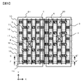
次に、第3の実施形態について、図11を参照して説明する。
図11は、メタル配線層を3層で構成した第3の実施形態における半導体装置の平面図である。3層目のドレイン側メタル配線層30と3層目のソース側メタル配線層31が向き合う方向に、ドレイン側の2層目のメタル配線層20及びソース側の2層目のメタル配線層21が延伸している。2層目のメタル配線層20、21と交差するように1層目のメタル配線層10、11が並設されている。
(1)トランジスタ層上の電流密度を均一化することにより、トランジスタ層の入力部または出力部に接続されるメタル配線層に対し、局所的な電流密度上昇を抑えることができ、エレクトロマイグレーションによる劣化を抑制できる。一般に、トランジスタ層の電流密度が均一でない場合、トランジスタ層において電流密度が高い領域に配置されたトランジスタに接続しているメタル配線層は電流密度が高くなるため、このメタル配線層はエレクトロマイグレーションにより寿命が低下する。一方、本実施形態では、トランジスタ層の電流密度を均一化することにより、メタル配線層のエレクトロマイグレーションに起因する寿命を長くすることができ、半導体装置としての信頼性を向上することができる。
次に、第1~第3の実施形態で示した半導体装置を負荷駆動装置に適用した例を説明する。図12は、負荷駆動装置91の回路構成を示す図である。同図において、第1~第3の実施形態で示した半導体装置はスイッチング素子92に相当する。
(1)半導体装置は、ドレイン電極Dとソース電極Sとゲート電極Gとを有する複数のトランジスタが2次元状に配置されたトランジスタ層1と、トランジスタ層1の複数のトランジスタのドレイン電極Dを入力端子に電気的に接続し、ソース電極Sを出力端子に電気的に接続するための複数の配線層と、複数の配線層およびトランジスタ層1の間をそれぞれ接続する複数の層間接続導体と、を備える。複数の配線層は、2層目の配線層として、入力端子用パッド7を介して入力端子に接続される入力側配線層であるメタル配線層20と、出力端子用パッド8を介して出力端子に接続される出力側配線層であるメタル配線層21とが、所定の配列方向に沿って配列されている配線層を有する。そして、複数の層間接続導体の抵抗値は、メタル配線層20、21の配列方向の位置に応じて互いに異なる。具体的には、複数の配線層は、メタル配線層20、21を含む2層目の配線層と、この配線層よりもトランジスタ層1側に設けられ、複数のメタル配線層10、11を有する1層目の配線層とを有する。複数の層間接続導体は、メタル配線層10、l1とトランジスタ層1の複数のトランジスタのドレイン電極Dおよびソース電極Sとを接続する複数のスルーホール群2、3を有する。この複数のスルーホール群2、3の抵抗値は、メタル配線層20、21の配列方向の位置に応じて互いに異なる。これにより、2次元に拡がって配置されたトランジスタの電流密度を均一にすることができる。
2、3 スルーホール群
7 入力端子用パッド
8 出力端子用パッド
10、11 1層目のメタル配線層
20、21 2層目のメタル配線層
30、31 3層目のメタル配線層
Id、Is 電流、
D ドレイン電極、
S ソース電極、
G ゲート電極
91 負荷駆動装置
92 スイッチング素子
93 ゲート駆動回路
94 負荷
Claims (10)
- 入力部と出力部と制御部とを有する複数のトランジスタが2次元状に配置されたトランジスタ層と、
前記複数のトランジスタの前記入力部を入力端子に電気的に接続し、前記複数のトランジスタの前記出力部を出力端子に電気的に接続するための複数の配線層と、
前記複数の配線層および前記トランジスタ層の間をそれぞれ接続する複数の層間接続導体と、を備え、
前記複数の配線層は、前記入力端子に接続される少なくとも1つの入力側配線層と前記出力端子に接続される少なくとも1つの出力側配線層とが所定の配列方向に沿って配列された第1配線層を有し、
前記複数の層間接続導体の抵抗値は、前記配列方向の位置に応じて互いに異なる半導体装置。 - 請求項1に記載の半導体装置において、
前記複数の配線層は、前記第1配線層と、前記第1配線層よりも前記トランジスタ層側に設けられた第2配線層とを有し、
前記複数の層間接続導体は、前記第2配線層と前記複数のトランジスタの前記入力部および前記出力部とを接続する複数の第1層間接続導体を有し、
前記複数の第1層間接続導体の抵抗値は、前記配列方向の位置に応じて互いに異なる半導体装置。 - 請求項2に記載の半導体装置において、
前記複数の第1層間接続導体の抵抗値は、少なくとも前記第2配線層の配線長に基づいて変化する半導体装置。 - 請求項3に記載の半導体装置において、
前記複数の層間接続導体は、前記複数の第1層間接続導体と、前記第1配線層と前記第2配線層とを接続する第2層間接続導体とを有し、
前記第2配線層の配線長は、前記第2層間接続導体の位置を始点とする半導体装置。 - 請求項2に記載の半導体装置において、
前記第1層間接続導体の抵抗値は、前記入力側配線層と前記出力側配線層との境界に近いほど高い半導体装置。 - 請求項2に記載の半導体装置において、
前記第1配線層は、2つの前記入力側配線層と1つの前記出力側配線層とが、または1つの前記入力側配線層と2つの前記出力側配線層とが、前記配列方向に沿って交互に配列されており、
前記第1層間接続導体の抵抗値は、2つの前記入力側配線層の間に配置された1つの前記出力側配線層において前記配列方向に直交する中心線、または2つの前記出力側配線層の間に配置された1つの前記入力側配線層において前記配列方向に直交する中心線に近いほど低い半導体装置。 - 請求項2~6のいずれか1項に記載の半導体装置において、
前記複数の第1層間接続導体は、複数の接続導体によってそれぞれ構成され、
前記複数の第1層間接続導体の抵抗値は、各第1層間接続導体を構成する前記接続導体の分布密度によって変化する半導体装置。 - 請求項2~7のいずれか1項に記載の半導体装置において、
前記第1配線層の配線抵抗は前記第2配線層の配線抵抗よりも低い半導体装置。 - 請求項1~8のいずれか1項に記載の半導体装置を少なくとも一つ、同一の半導体チップに実装した半導体集積回路。
- 請求項1~8のいずれか1項に記載の半導体装置をスイッチング素子として、前記スイッチング素子の制御部に電圧を印加して、前記スイッチング素子に接続された負荷を駆動する負荷駆動装置。
Priority Applications (4)
| Application Number | Priority Date | Filing Date | Title |
|---|---|---|---|
| EP16838989.8A EP3340284B1 (en) | 2015-08-21 | 2016-07-25 | Semiconductor device, semiconductor integrated circuit, and load driving device |
| JP2017536693A JP6546995B2 (ja) | 2015-08-21 | 2016-07-25 | 半導体装置、半導体集積回路、及び負荷駆動装置 |
| US15/752,818 US10170415B2 (en) | 2015-08-21 | 2016-07-25 | Semiconductor device, semiconductor integrated circuit, and load driving device |
| CN201680045783.2A CN107851583B (zh) | 2015-08-21 | 2016-07-25 | 半导体装置、半导体集成电路以及负载驱动装置 |
Applications Claiming Priority (2)
| Application Number | Priority Date | Filing Date | Title |
|---|---|---|---|
| JP2015163319 | 2015-08-21 | ||
| JP2015-163319 | 2015-08-21 |
Publications (1)
| Publication Number | Publication Date |
|---|---|
| WO2017033642A1 true WO2017033642A1 (ja) | 2017-03-02 |
Family
ID=58099903
Family Applications (1)
| Application Number | Title | Priority Date | Filing Date |
|---|---|---|---|
| PCT/JP2016/071658 Ceased WO2017033642A1 (ja) | 2015-08-21 | 2016-07-25 | 半導体装置、半導体集積回路、及び負荷駆動装置 |
Country Status (5)
| Country | Link |
|---|---|
| US (1) | US10170415B2 (ja) |
| EP (1) | EP3340284B1 (ja) |
| JP (1) | JP6546995B2 (ja) |
| CN (1) | CN107851583B (ja) |
| WO (1) | WO2017033642A1 (ja) |
Cited By (2)
| Publication number | Priority date | Publication date | Assignee | Title |
|---|---|---|---|---|
| JP2020043302A (ja) * | 2018-09-13 | 2020-03-19 | 株式会社東芝 | 半導体装置 |
| WO2022244700A1 (ja) * | 2021-05-17 | 2022-11-24 | 株式会社村田製作所 | 半導体装置 |
Families Citing this family (3)
| Publication number | Priority date | Publication date | Assignee | Title |
|---|---|---|---|---|
| DE102015217426A1 (de) * | 2015-09-11 | 2017-03-16 | Zf Friedrichshafen Ag | Mehrfunktionale Hochstromleiterplatte |
| CN108879634B (zh) * | 2018-06-30 | 2022-03-04 | 唯捷创芯(天津)电子技术股份有限公司 | 一种浪涌保护器件及其组成的芯片、通信终端 |
| US12087759B2 (en) * | 2021-06-30 | 2024-09-10 | Alpha And Omega Semiconductor International Lp | Low capacitance two channel and multi-channel TVS with effective inter-connection |
Citations (6)
| Publication number | Priority date | Publication date | Assignee | Title |
|---|---|---|---|---|
| JPH0745829A (ja) * | 1993-07-28 | 1995-02-14 | Ricoh Co Ltd | 半導体集積回路装置 |
| JP2000216264A (ja) * | 1999-01-22 | 2000-08-04 | Mitsubishi Electric Corp | Cmos論理回路素子、半導体装置とその製造方法およびその製造方法において用いる半導体回路設計方法 |
| JP2006515956A (ja) * | 2002-10-08 | 2006-06-08 | グレイト・ウォール・セミコンダクター・コーポレイション | パワーmosfet |
| JP2006278677A (ja) * | 2005-03-29 | 2006-10-12 | Mitsumi Electric Co Ltd | 半導体装置 |
| JP2009246076A (ja) * | 2008-03-31 | 2009-10-22 | Sanyo Electric Co Ltd | パワー半導体装置 |
| JP2010219504A (ja) * | 2009-02-23 | 2010-09-30 | Seiko Instruments Inc | 半導体装置 |
Family Cites Families (9)
| Publication number | Priority date | Publication date | Assignee | Title |
|---|---|---|---|---|
| KR100203900B1 (ko) * | 1996-06-24 | 1999-06-15 | 김영환 | 정전기 보호회로를 구비한 반도체장치 |
| US6468889B1 (en) * | 2000-08-08 | 2002-10-22 | Advanced Micro Devices, Inc. | Backside contact for integrated circuit and method of forming same |
| JP2007173731A (ja) * | 2005-12-26 | 2007-07-05 | Mitsumi Electric Co Ltd | 半導体装置 |
| JP2008227227A (ja) * | 2007-03-14 | 2008-09-25 | Seiko Epson Corp | 半導体装置及びその製造方法 |
| DE102007020258B4 (de) * | 2007-04-30 | 2018-06-28 | Globalfoundries Inc. | Technik zur Verbesserung des Transistorleitungsverhaltens durch eine transistorspezifische Kontaktgestaltung |
| JP2009044085A (ja) * | 2007-08-10 | 2009-02-26 | Mitsumi Electric Co Ltd | Mosトランジスタ及びこれを用いた半導体集積回路装置 |
| JP5165967B2 (ja) * | 2007-08-22 | 2013-03-21 | セイコーインスツル株式会社 | 半導体装置 |
| JP5438947B2 (ja) * | 2007-11-27 | 2014-03-12 | 株式会社東芝 | 半導体装置 |
| US8138557B2 (en) * | 2009-11-11 | 2012-03-20 | Green Solution Technology Co., Ltd. | Layout structure of MOSFET and layout method thereof |
-
2016
- 2016-07-25 JP JP2017536693A patent/JP6546995B2/ja active Active
- 2016-07-25 WO PCT/JP2016/071658 patent/WO2017033642A1/ja not_active Ceased
- 2016-07-25 US US15/752,818 patent/US10170415B2/en active Active
- 2016-07-25 EP EP16838989.8A patent/EP3340284B1/en active Active
- 2016-07-25 CN CN201680045783.2A patent/CN107851583B/zh active Active
Patent Citations (6)
| Publication number | Priority date | Publication date | Assignee | Title |
|---|---|---|---|---|
| JPH0745829A (ja) * | 1993-07-28 | 1995-02-14 | Ricoh Co Ltd | 半導体集積回路装置 |
| JP2000216264A (ja) * | 1999-01-22 | 2000-08-04 | Mitsubishi Electric Corp | Cmos論理回路素子、半導体装置とその製造方法およびその製造方法において用いる半導体回路設計方法 |
| JP2006515956A (ja) * | 2002-10-08 | 2006-06-08 | グレイト・ウォール・セミコンダクター・コーポレイション | パワーmosfet |
| JP2006278677A (ja) * | 2005-03-29 | 2006-10-12 | Mitsumi Electric Co Ltd | 半導体装置 |
| JP2009246076A (ja) * | 2008-03-31 | 2009-10-22 | Sanyo Electric Co Ltd | パワー半導体装置 |
| JP2010219504A (ja) * | 2009-02-23 | 2010-09-30 | Seiko Instruments Inc | 半導体装置 |
Non-Patent Citations (1)
| Title |
|---|
| See also references of EP3340284A4 * |
Cited By (3)
| Publication number | Priority date | Publication date | Assignee | Title |
|---|---|---|---|---|
| JP2020043302A (ja) * | 2018-09-13 | 2020-03-19 | 株式会社東芝 | 半導体装置 |
| US11908897B2 (en) | 2018-09-13 | 2024-02-20 | Kabushiki Kaisha Toshiba | Semiconductor device having two-dimensional MOSFET |
| WO2022244700A1 (ja) * | 2021-05-17 | 2022-11-24 | 株式会社村田製作所 | 半導体装置 |
Also Published As
| Publication number | Publication date |
|---|---|
| US10170415B2 (en) | 2019-01-01 |
| JP6546995B2 (ja) | 2019-07-17 |
| JPWO2017033642A1 (ja) | 2018-03-01 |
| CN107851583A (zh) | 2018-03-27 |
| EP3340284B1 (en) | 2025-04-09 |
| EP3340284A4 (en) | 2019-03-20 |
| CN107851583B (zh) | 2021-04-02 |
| EP3340284A1 (en) | 2018-06-27 |
| US20180247892A1 (en) | 2018-08-30 |
Similar Documents
| Publication | Publication Date | Title |
|---|---|---|
| JP6546995B2 (ja) | 半導体装置、半導体集積回路、及び負荷駆動装置 | |
| JP6115050B2 (ja) | 半導体装置 | |
| US10157922B2 (en) | Interconnect metal layout for integrated circuit | |
| US20170179112A1 (en) | Semiconductor device | |
| KR20100096027A (ko) | 반도체 장치 | |
| US7687912B2 (en) | Semiconductor component comprising interconnected cell strips | |
| US20160071798A1 (en) | Semiconductor Device | |
| US9450089B2 (en) | Semiconductor device | |
| US10559528B2 (en) | Semiconductor device including external terminal groups | |
| JP2016035966A (ja) | 半導体集積回路装置 | |
| US8878203B2 (en) | Switching circuit | |
| US11145646B2 (en) | Semiconductor device | |
| JP2006269835A (ja) | 半導体装置 | |
| US20100059795A1 (en) | Vertical current transport in a power converter circuit | |
| KR102082644B1 (ko) | 반도체 장치 | |
| CN105097756B (zh) | 半导体模块 | |
| CN114843251B (zh) | 半导体器件结构及其制备方法 | |
| US12114423B2 (en) | Circuit board and probe card | |
| US12300606B2 (en) | Mirror circuit devices with wide wirings | |
| US20240429915A1 (en) | Asymmetric power module | |
| CN114678338B (zh) | 集成电路组件及其封装组件 | |
| WO2025062688A1 (ja) | 半導体装置 | |
| JP6838240B2 (ja) | 電子装置 | |
| DE102022213627A1 (de) | Leistungsmodul | |
| EP2916356B1 (en) | Amplifier structure |
Legal Events
| Date | Code | Title | Description |
|---|---|---|---|
| 121 | Ep: the epo has been informed by wipo that ep was designated in this application |
Ref document number: 16838989 Country of ref document: EP Kind code of ref document: A1 |
|
| ENP | Entry into the national phase |
Ref document number: 2017536693 Country of ref document: JP Kind code of ref document: A |
|
| WWE | Wipo information: entry into national phase |
Ref document number: 15752818 Country of ref document: US |
|
| NENP | Non-entry into the national phase |
Ref country code: DE |
|
| WWG | Wipo information: grant in national office |
Ref document number: 2016838989 Country of ref document: EP |