WO2017038085A1 - 画像表示装置 - Google Patents
画像表示装置 Download PDFInfo
- Publication number
- WO2017038085A1 WO2017038085A1 PCT/JP2016/003945 JP2016003945W WO2017038085A1 WO 2017038085 A1 WO2017038085 A1 WO 2017038085A1 JP 2016003945 W JP2016003945 W JP 2016003945W WO 2017038085 A1 WO2017038085 A1 WO 2017038085A1
- Authority
- WO
- WIPO (PCT)
- Prior art keywords
- light source
- image display
- display device
- source substrate
- main surface
- Prior art date
- Legal status (The legal status is an assumption and is not a legal conclusion. Google has not performed a legal analysis and makes no representation as to the accuracy of the status listed.)
- Ceased
Links
Images






Classifications
-
- G—PHYSICS
- G02—OPTICS
- G02F—OPTICAL DEVICES OR ARRANGEMENTS FOR THE CONTROL OF LIGHT BY MODIFICATION OF THE OPTICAL PROPERTIES OF THE MEDIA OF THE ELEMENTS INVOLVED THEREIN; NON-LINEAR OPTICS; FREQUENCY-CHANGING OF LIGHT; OPTICAL LOGIC ELEMENTS; OPTICAL ANALOGUE/DIGITAL CONVERTERS
- G02F1/00—Devices or arrangements for the control of the intensity, colour, phase, polarisation or direction of light arriving from an independent light source, e.g. switching, gating or modulating; Non-linear optics
- G02F1/01—Devices or arrangements for the control of the intensity, colour, phase, polarisation or direction of light arriving from an independent light source, e.g. switching, gating or modulating; Non-linear optics for the control of the intensity, phase, polarisation or colour
- G02F1/13—Devices or arrangements for the control of the intensity, colour, phase, polarisation or direction of light arriving from an independent light source, e.g. switching, gating or modulating; Non-linear optics for the control of the intensity, phase, polarisation or colour based on liquid crystals, e.g. single liquid crystal display cells
- G02F1/133—Constructional arrangements; Operation of liquid crystal cells; Circuit arrangements
- G02F1/1333—Constructional arrangements; Manufacturing methods
- G02F1/1335—Structural association of cells with optical devices, e.g. polarisers or reflectors
- G02F1/1336—Illuminating devices
- G02F1/133602—Direct backlight
- G02F1/133603—Direct backlight with LEDs
-
- F—MECHANICAL ENGINEERING; LIGHTING; HEATING; WEAPONS; BLASTING
- F21—LIGHTING
- F21S—NON-PORTABLE LIGHTING DEVICES; SYSTEMS THEREOF; VEHICLE LIGHTING DEVICES SPECIALLY ADAPTED FOR VEHICLE EXTERIORS
- F21S2/00—Systems of lighting devices, not provided for in main groups F21S4/00 - F21S10/00 or F21S19/00, e.g. of modular construction
-
- F—MECHANICAL ENGINEERING; LIGHTING; HEATING; WEAPONS; BLASTING
- F21—LIGHTING
- F21V—FUNCTIONAL FEATURES OR DETAILS OF LIGHTING DEVICES OR SYSTEMS THEREOF; STRUCTURAL COMBINATIONS OF LIGHTING DEVICES WITH OTHER ARTICLES, NOT OTHERWISE PROVIDED FOR
- F21V19/00—Fastening of light sources or lamp holders
-
- F—MECHANICAL ENGINEERING; LIGHTING; HEATING; WEAPONS; BLASTING
- F21—LIGHTING
- F21V—FUNCTIONAL FEATURES OR DETAILS OF LIGHTING DEVICES OR SYSTEMS THEREOF; STRUCTURAL COMBINATIONS OF LIGHTING DEVICES WITH OTHER ARTICLES, NOT OTHERWISE PROVIDED FOR
- F21V23/00—Arrangement of electric circuit elements in or on lighting devices
-
- F—MECHANICAL ENGINEERING; LIGHTING; HEATING; WEAPONS; BLASTING
- F21—LIGHTING
- F21V—FUNCTIONAL FEATURES OR DETAILS OF LIGHTING DEVICES OR SYSTEMS THEREOF; STRUCTURAL COMBINATIONS OF LIGHTING DEVICES WITH OTHER ARTICLES, NOT OTHERWISE PROVIDED FOR
- F21V23/00—Arrangement of electric circuit elements in or on lighting devices
- F21V23/06—Arrangement of electric circuit elements in or on lighting devices the elements being coupling devices, e.g. connectors
-
- G—PHYSICS
- G02—OPTICS
- G02F—OPTICAL DEVICES OR ARRANGEMENTS FOR THE CONTROL OF LIGHT BY MODIFICATION OF THE OPTICAL PROPERTIES OF THE MEDIA OF THE ELEMENTS INVOLVED THEREIN; NON-LINEAR OPTICS; FREQUENCY-CHANGING OF LIGHT; OPTICAL LOGIC ELEMENTS; OPTICAL ANALOGUE/DIGITAL CONVERTERS
- G02F1/00—Devices or arrangements for the control of the intensity, colour, phase, polarisation or direction of light arriving from an independent light source, e.g. switching, gating or modulating; Non-linear optics
- G02F1/01—Devices or arrangements for the control of the intensity, colour, phase, polarisation or direction of light arriving from an independent light source, e.g. switching, gating or modulating; Non-linear optics for the control of the intensity, phase, polarisation or colour
- G02F1/13—Devices or arrangements for the control of the intensity, colour, phase, polarisation or direction of light arriving from an independent light source, e.g. switching, gating or modulating; Non-linear optics for the control of the intensity, phase, polarisation or colour based on liquid crystals, e.g. single liquid crystal display cells
- G02F1/133—Constructional arrangements; Operation of liquid crystal cells; Circuit arrangements
- G02F1/13306—Circuit arrangements or driving methods for the control of single liquid crystal cells
-
- G—PHYSICS
- G02—OPTICS
- G02F—OPTICAL DEVICES OR ARRANGEMENTS FOR THE CONTROL OF LIGHT BY MODIFICATION OF THE OPTICAL PROPERTIES OF THE MEDIA OF THE ELEMENTS INVOLVED THEREIN; NON-LINEAR OPTICS; FREQUENCY-CHANGING OF LIGHT; OPTICAL LOGIC ELEMENTS; OPTICAL ANALOGUE/DIGITAL CONVERTERS
- G02F1/00—Devices or arrangements for the control of the intensity, colour, phase, polarisation or direction of light arriving from an independent light source, e.g. switching, gating or modulating; Non-linear optics
- G02F1/01—Devices or arrangements for the control of the intensity, colour, phase, polarisation or direction of light arriving from an independent light source, e.g. switching, gating or modulating; Non-linear optics for the control of the intensity, phase, polarisation or colour
- G02F1/13—Devices or arrangements for the control of the intensity, colour, phase, polarisation or direction of light arriving from an independent light source, e.g. switching, gating or modulating; Non-linear optics for the control of the intensity, phase, polarisation or colour based on liquid crystals, e.g. single liquid crystal display cells
- G02F1/133—Constructional arrangements; Operation of liquid crystal cells; Circuit arrangements
- G02F1/1333—Constructional arrangements; Manufacturing methods
- G02F1/133308—Support structures for LCD panels, e.g. frames or bezels
-
- G—PHYSICS
- G09—EDUCATION; CRYPTOGRAPHY; DISPLAY; ADVERTISING; SEALS
- G09F—DISPLAYING; ADVERTISING; SIGNS; LABELS OR NAME-PLATES; SEALS
- G09F9/00—Indicating arrangements for variable information in which the information is built-up on a support by selection or combination of individual elements
-
- G—PHYSICS
- G09—EDUCATION; CRYPTOGRAPHY; DISPLAY; ADVERTISING; SEALS
- G09G—ARRANGEMENTS OR CIRCUITS FOR CONTROL OF INDICATING DEVICES USING STATIC MEANS TO PRESENT VARIABLE INFORMATION
- G09G3/00—Control arrangements or circuits, of interest only in connection with visual indicators other than cathode-ray tubes
- G09G3/20—Control arrangements or circuits, of interest only in connection with visual indicators other than cathode-ray tubes for presentation of an assembly of a number of characters, e.g. a page, by composing the assembly by combination of individual elements arranged in a matrix no fixed position being assigned to or needed to be assigned to the individual characters or partial characters
-
- G—PHYSICS
- G09—EDUCATION; CRYPTOGRAPHY; DISPLAY; ADVERTISING; SEALS
- G09G—ARRANGEMENTS OR CIRCUITS FOR CONTROL OF INDICATING DEVICES USING STATIC MEANS TO PRESENT VARIABLE INFORMATION
- G09G3/00—Control arrangements or circuits, of interest only in connection with visual indicators other than cathode-ray tubes
- G09G3/20—Control arrangements or circuits, of interest only in connection with visual indicators other than cathode-ray tubes for presentation of an assembly of a number of characters, e.g. a page, by composing the assembly by combination of individual elements arranged in a matrix no fixed position being assigned to or needed to be assigned to the individual characters or partial characters
- G09G3/34—Control arrangements or circuits, of interest only in connection with visual indicators other than cathode-ray tubes for presentation of an assembly of a number of characters, e.g. a page, by composing the assembly by combination of individual elements arranged in a matrix no fixed position being assigned to or needed to be assigned to the individual characters or partial characters by control of light from an independent source
-
- G—PHYSICS
- G09—EDUCATION; CRYPTOGRAPHY; DISPLAY; ADVERTISING; SEALS
- G09G—ARRANGEMENTS OR CIRCUITS FOR CONTROL OF INDICATING DEVICES USING STATIC MEANS TO PRESENT VARIABLE INFORMATION
- G09G3/00—Control arrangements or circuits, of interest only in connection with visual indicators other than cathode-ray tubes
- G09G3/20—Control arrangements or circuits, of interest only in connection with visual indicators other than cathode-ray tubes for presentation of an assembly of a number of characters, e.g. a page, by composing the assembly by combination of individual elements arranged in a matrix no fixed position being assigned to or needed to be assigned to the individual characters or partial characters
- G09G3/34—Control arrangements or circuits, of interest only in connection with visual indicators other than cathode-ray tubes for presentation of an assembly of a number of characters, e.g. a page, by composing the assembly by combination of individual elements arranged in a matrix no fixed position being assigned to or needed to be assigned to the individual characters or partial characters by control of light from an independent source
- G09G3/36—Control arrangements or circuits, of interest only in connection with visual indicators other than cathode-ray tubes for presentation of an assembly of a number of characters, e.g. a page, by composing the assembly by combination of individual elements arranged in a matrix no fixed position being assigned to or needed to be assigned to the individual characters or partial characters by control of light from an independent source using liquid crystals
-
- H—ELECTRICITY
- H05—ELECTRIC TECHNIQUES NOT OTHERWISE PROVIDED FOR
- H05K—PRINTED CIRCUITS; CASINGS OR CONSTRUCTIONAL DETAILS OF ELECTRIC APPARATUS; MANUFACTURE OF ASSEMBLAGES OF ELECTRICAL COMPONENTS
- H05K1/00—Printed circuits
- H05K1/02—Details
- H05K1/0201—Thermal arrangements, e.g. for cooling, heating or preventing overheating
- H05K1/0203—Cooling of mounted components
- H05K1/0209—External configuration of printed circuit board adapted for heat dissipation, e.g. lay-out of conductors, coatings
-
- H—ELECTRICITY
- H05—ELECTRIC TECHNIQUES NOT OTHERWISE PROVIDED FOR
- H05K—PRINTED CIRCUITS; CASINGS OR CONSTRUCTIONAL DETAILS OF ELECTRIC APPARATUS; MANUFACTURE OF ASSEMBLAGES OF ELECTRICAL COMPONENTS
- H05K1/00—Printed circuits
- H05K1/02—Details
- H05K1/0213—Electrical arrangements not otherwise provided for
- H05K1/0263—High current adaptations, e.g. printed high current conductors or using auxiliary non-printed means; Fine and coarse circuit patterns on one circuit board
-
- H—ELECTRICITY
- H05—ELECTRIC TECHNIQUES NOT OTHERWISE PROVIDED FOR
- H05K—PRINTED CIRCUITS; CASINGS OR CONSTRUCTIONAL DETAILS OF ELECTRIC APPARATUS; MANUFACTURE OF ASSEMBLAGES OF ELECTRICAL COMPONENTS
- H05K1/00—Printed circuits
- H05K1/02—Details
- H05K1/0271—Arrangements for reducing stress or warp in rigid printed circuit boards, e.g. caused by loads, vibrations or differences in thermal expansion
-
- G—PHYSICS
- G02—OPTICS
- G02F—OPTICAL DEVICES OR ARRANGEMENTS FOR THE CONTROL OF LIGHT BY MODIFICATION OF THE OPTICAL PROPERTIES OF THE MEDIA OF THE ELEMENTS INVOLVED THEREIN; NON-LINEAR OPTICS; FREQUENCY-CHANGING OF LIGHT; OPTICAL LOGIC ELEMENTS; OPTICAL ANALOGUE/DIGITAL CONVERTERS
- G02F1/00—Devices or arrangements for the control of the intensity, colour, phase, polarisation or direction of light arriving from an independent light source, e.g. switching, gating or modulating; Non-linear optics
- G02F1/01—Devices or arrangements for the control of the intensity, colour, phase, polarisation or direction of light arriving from an independent light source, e.g. switching, gating or modulating; Non-linear optics for the control of the intensity, phase, polarisation or colour
- G02F1/13—Devices or arrangements for the control of the intensity, colour, phase, polarisation or direction of light arriving from an independent light source, e.g. switching, gating or modulating; Non-linear optics for the control of the intensity, phase, polarisation or colour based on liquid crystals, e.g. single liquid crystal display cells
- G02F1/133—Constructional arrangements; Operation of liquid crystal cells; Circuit arrangements
- G02F1/1333—Constructional arrangements; Manufacturing methods
- G02F1/1335—Structural association of cells with optical devices, e.g. polarisers or reflectors
- G02F1/1336—Illuminating devices
- G02F1/133601—Illuminating devices for spatial active dimming
-
- G—PHYSICS
- G02—OPTICS
- G02F—OPTICAL DEVICES OR ARRANGEMENTS FOR THE CONTROL OF LIGHT BY MODIFICATION OF THE OPTICAL PROPERTIES OF THE MEDIA OF THE ELEMENTS INVOLVED THEREIN; NON-LINEAR OPTICS; FREQUENCY-CHANGING OF LIGHT; OPTICAL LOGIC ELEMENTS; OPTICAL ANALOGUE/DIGITAL CONVERTERS
- G02F1/00—Devices or arrangements for the control of the intensity, colour, phase, polarisation or direction of light arriving from an independent light source, e.g. switching, gating or modulating; Non-linear optics
- G02F1/01—Devices or arrangements for the control of the intensity, colour, phase, polarisation or direction of light arriving from an independent light source, e.g. switching, gating or modulating; Non-linear optics for the control of the intensity, phase, polarisation or colour
- G02F1/13—Devices or arrangements for the control of the intensity, colour, phase, polarisation or direction of light arriving from an independent light source, e.g. switching, gating or modulating; Non-linear optics for the control of the intensity, phase, polarisation or colour based on liquid crystals, e.g. single liquid crystal display cells
- G02F1/133—Constructional arrangements; Operation of liquid crystal cells; Circuit arrangements
- G02F1/1333—Constructional arrangements; Manufacturing methods
- G02F1/1335—Structural association of cells with optical devices, e.g. polarisers or reflectors
- G02F1/1336—Illuminating devices
- G02F1/133602—Direct backlight
- G02F1/133612—Electrical details
-
- G—PHYSICS
- G02—OPTICS
- G02F—OPTICAL DEVICES OR ARRANGEMENTS FOR THE CONTROL OF LIGHT BY MODIFICATION OF THE OPTICAL PROPERTIES OF THE MEDIA OF THE ELEMENTS INVOLVED THEREIN; NON-LINEAR OPTICS; FREQUENCY-CHANGING OF LIGHT; OPTICAL LOGIC ELEMENTS; OPTICAL ANALOGUE/DIGITAL CONVERTERS
- G02F1/00—Devices or arrangements for the control of the intensity, colour, phase, polarisation or direction of light arriving from an independent light source, e.g. switching, gating or modulating; Non-linear optics
- G02F1/01—Devices or arrangements for the control of the intensity, colour, phase, polarisation or direction of light arriving from an independent light source, e.g. switching, gating or modulating; Non-linear optics for the control of the intensity, phase, polarisation or colour
- G02F1/13—Devices or arrangements for the control of the intensity, colour, phase, polarisation or direction of light arriving from an independent light source, e.g. switching, gating or modulating; Non-linear optics for the control of the intensity, phase, polarisation or colour based on liquid crystals, e.g. single liquid crystal display cells
- G02F1/133—Constructional arrangements; Operation of liquid crystal cells; Circuit arrangements
- G02F1/1333—Constructional arrangements; Manufacturing methods
- G02F1/1335—Structural association of cells with optical devices, e.g. polarisers or reflectors
- G02F1/1336—Illuminating devices
- G02F1/133628—Illuminating devices with cooling means
-
- H—ELECTRICITY
- H05—ELECTRIC TECHNIQUES NOT OTHERWISE PROVIDED FOR
- H05K—PRINTED CIRCUITS; CASINGS OR CONSTRUCTIONAL DETAILS OF ELECTRIC APPARATUS; MANUFACTURE OF ASSEMBLAGES OF ELECTRICAL COMPONENTS
- H05K2201/00—Indexing scheme relating to printed circuits covered by H05K1/00
- H05K2201/09—Shape and layout
- H05K2201/09009—Substrate related
- H05K2201/09136—Means for correcting warpage
-
- H—ELECTRICITY
- H05—ELECTRIC TECHNIQUES NOT OTHERWISE PROVIDED FOR
- H05K—PRINTED CIRCUITS; CASINGS OR CONSTRUCTIONAL DETAILS OF ELECTRIC APPARATUS; MANUFACTURE OF ASSEMBLAGES OF ELECTRICAL COMPONENTS
- H05K2201/00—Indexing scheme relating to printed circuits covered by H05K1/00
- H05K2201/09—Shape and layout
- H05K2201/09209—Shape and layout details of conductors
- H05K2201/09654—Shape and layout details of conductors covering at least two types of conductors provided for in H05K2201/09218 - H05K2201/095
- H05K2201/09672—Superposed layout, i.e. in different planes
-
- H—ELECTRICITY
- H05—ELECTRIC TECHNIQUES NOT OTHERWISE PROVIDED FOR
- H05K—PRINTED CIRCUITS; CASINGS OR CONSTRUCTIONAL DETAILS OF ELECTRIC APPARATUS; MANUFACTURE OF ASSEMBLAGES OF ELECTRICAL COMPONENTS
- H05K2201/00—Indexing scheme relating to printed circuits covered by H05K1/00
- H05K2201/10—Details of components or other objects attached to or integrated in a printed circuit board
- H05K2201/10007—Types of components
- H05K2201/10106—Light emitting diode [LED]
-
- H—ELECTRICITY
- H05—ELECTRIC TECHNIQUES NOT OTHERWISE PROVIDED FOR
- H05K—PRINTED CIRCUITS; CASINGS OR CONSTRUCTIONAL DETAILS OF ELECTRIC APPARATUS; MANUFACTURE OF ASSEMBLAGES OF ELECTRICAL COMPONENTS
- H05K2201/00—Indexing scheme relating to printed circuits covered by H05K1/00
- H05K2201/10—Details of components or other objects attached to or integrated in a printed circuit board
- H05K2201/10007—Types of components
- H05K2201/10128—Display
- H05K2201/10136—Liquid Crystal display [LCD]
Definitions
- the present disclosure relates to an image display device having a backlight.
- an image display device having a backlight such as a liquid crystal display device
- various techniques for improving the image quality are continuously developed.
- An example of such a technique is a technique called local dimming.
- Patent Document 1 discloses a technique related to local dimming.
- Local dimming is a technology that divides a liquid crystal display panel into a plurality of areas and dimmes a plurality of light sources arranged corresponding to the areas according to the brightness of the image displayed on each area of the liquid crystal display panel. is there. With this technique, the contrast of an image in one screen can be improved.
- the light source for example, an LED (Light Emitting Diode) is used.
- the present disclosure provides an image display device that includes a plurality of LEDs that can be dimmed independently of each other, can be downsized and thinned, and can reduce assembly costs, and is suitable for heat management. To do.
- the image display device includes a liquid crystal display panel and a light source substrate for illuminating the liquid crystal display panel from the back.
- the light source substrate includes a plurality of light emitting diodes each provided corresponding to a different area of the liquid crystal display panel, and each of the plurality of light emitting diodes has a luminance according to the brightness in the corresponding area of the image according to the control signal
- a driver element that is driven by A first conductor foil is disposed on the first main surface on which the light emitting diodes of the light source substrate are mounted, and a second conductor foil is disposed on the second main surface opposite to the first main surface.
- a ground pattern foil is disposed as a second conductor foil in a region including each of the plurality of light emitting diodes in plan view on the second main surface.
- the area of the first conductor foil and the area of the second conductor foil are substantially equal to each other.
- the image display device since a plurality of light emitting diodes and a plurality of driver elements are mounted on one light source substrate, the number of substrates and cables can be reduced, and the device can be reduced in size, thickness, and assembly cost can be reduced. It becomes possible.
- the ground pattern foil is disposed in the region corresponding to the light emitting diode on the second main surface of the light source substrate, the heat generated from the light emitting diode can be efficiently released to the outside.
- the conductor foils having substantially the same area are disposed on the first main surface and the second main surface of the light source substrate, it is possible to achieve both good heat dissipation and suppression of warpage in the light source substrate.
- FIG. 1 is a diagram schematically illustrating an example of the appearance of the image display apparatus according to the first embodiment.
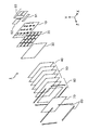
- FIG. 2 is an exploded perspective view schematically showing an example of the configuration of the image display apparatus according to the first embodiment.
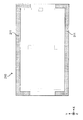
- FIG. 3 is a plan view schematically showing an example of the configuration of the light source substrate included in the image display device according to the first embodiment.
- FIG. 4 is a perspective view schematically showing an example of the shape of the reflection sheet provided in the image display device according to the first embodiment.
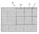
- FIG. 5 is a plan view schematically showing an example of the shape of a flutter included in the image display device in the first embodiment.
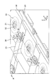
- FIG. 6 is a perspective view schematically showing an example of attaching the reflection sheet to the light source substrate in the image display apparatus according to the first embodiment.
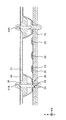
- FIG. 7 is a cross-sectional view schematically showing an example of the arrangement of members including the light source substrate, the reflection sheet, and the flutter in the image display apparatus according to the first embodiment.
- FIG. 8 is a cross-sectional view schematically showing an example of the arrangement of members including the light source substrate, the reflection sheet, and the flutter in the image display apparatus according to the first embodiment.
- FIG. 9 is a plan view schematically showing an example of the arrangement of connectors provided on the light source board in the image display apparatus according to the second embodiment.
- FIG. 10 is a plan view schematically showing an example of connection of a plurality of light source substrates constituting a backlight in the image display apparatus according to the second embodiment.
- FIG. 11 is a plan view schematically showing an example of the first conductor foil disposed on the first main surface of the light source substrate included in the image display device in the third embodiment.
- FIG. 12 is a plan view schematically showing an example of the second conductor foil disposed on the second main surface of the light source substrate included in the image display device in the third embodiment.
- FIG. 13 is a cross-sectional view schematically showing an example of the structure of the light source substrate included in the image display device in the third embodiment.
- FIG. 14 is a conceptual diagram illustrating an example of a power supply line formed by a power supply pattern foil on a light source substrate included in the image display device according to the third embodiment.
- FIG. 15 is a conceptual diagram showing an example of a power supply line formed by a power supply pattern foil on the light source substrate in the comparative example.
- FIG. 16 is a diagram for explaining the heat generation suppression effect by the light source substrate included in the image display device according to the third embodiment.
- the image display device includes a liquid crystal display panel and a light source substrate for illuminating the liquid crystal display panel from the back.
- the light source substrate includes a plurality of light emitting diodes each provided corresponding to a different area of the liquid crystal display panel, and each of the plurality of light emitting diodes has a luminance according to the brightness in the corresponding area of the image according to the control signal
- a driver element that is driven by A first conductor foil is disposed on the first main surface on which the light emitting diodes of the light source substrate are mounted, and a second conductor foil is disposed on the second main surface opposite to the first main surface.
- a ground pattern foil is disposed as a second conductor foil in a region including each of the plurality of light emitting diodes in plan view on the second main surface.
- the area of the first conductor foil and the area of the second conductor foil are substantially equal to each other.
- the number of substrates and cables can be reduced in the image display device, and the device can be reduced in size and thickness, and Assembly cost can be reduced.
- the ground pattern foil is disposed in the corresponding region of the light emitting diode on the second main surface of the light source substrate, the heat generated from the light emitting diode can be efficiently released to the outside. The wider the ground pattern foil on the second main surface, the higher the heat dissipation, but the greater the difference in area between the ground pattern foil and the conductor foil on the first main surface, the easier the light source substrate warps.
- the conductor foils having substantially the same area are arranged on the first main surface and the second main surface of the light source substrate, it is possible to achieve both good heat dissipation and suppression of warpage in the light source substrate.
- the image display device includes a liquid crystal display panel, a metal base plate, and a light source substrate that is attached to the base plate and illuminates the liquid crystal display panel from the back.
- the light source substrate includes a plurality of light emitting diodes each provided corresponding to a different area of the liquid crystal display panel, and each of the plurality of light emitting diodes has a luminance according to the brightness in the corresponding area of the image according to the control signal
- a driver element that is driven by A first conductor foil is disposed on the first main surface on which the light emitting diodes of the light source substrate are mounted, and a second conductor foil is disposed on the second main surface opposite to the first main surface. At least a portion of the second conductor foil is a ground pattern foil that is electrically connected to the base plate.
- the ground pattern foil on the second main surface is connected to the base plate, and the base plate is used as a part of the ground line, whereby the area of the ground pattern foil on the light source substrate can be reduced.
- the power supply pattern foil can be provided in a region obtained by reducing the ground pattern foil provided on the first main surface.
- 90% or more of the first conductor foil may be the power pattern foil in the area ratio.
- the first conductor foil on the first main surface is used as the power supply pattern foil, so that the voltage drop in the power supply line is reduced and the light emitting diode is driven with a lower power supply voltage. It becomes possible. Further, the heat generation (heat loss) in the driver element is reduced due to the reduction of the power supply voltage.
- the light source substrate may be attached to the base plate with a metal fastening member.
- the ground pattern foil may be electrically connected to the base plate via a fastening member.
- a base plate as a rigid base for holding the light source substrate can be used as a part of the ground line.
- a base plate having a relatively low electrical resistance as part of the ground line a voltage drop in the ground line is reduced, and the light emitting diode can be driven with a lower power supply voltage. Further, the heat generation (heat loss) in the driver element is reduced due to the reduction of the power supply voltage.
- the light source board may have a plurality of power connectors connected to different positions of the first conductor foil.
- the first conductive foil in the light source board is used as a part of the power line to supply power to the plurality of light source boards.
- the number of cables can be reduced compared to a configuration in which a plurality of light source substrates are not cascaded.
- driver element may be mounted on the first main surface.
- the light emitting diode and the driver element are mounted on the first main surface of the light source substrate, the work of mounting components on the light source substrate in the manufacturing process is compared with the case of mounting them on both surfaces. And it will be easy.
- a reflecting plate for guiding the light of each light emitting diode to the corresponding region is provided.
- the reflecting plate may have a bulge as a partition for reducing light leakage between regions corresponding to light emitting diodes adjacent to each other. If such a ridge is made hollow and the driver element is stored in the ridge, it is possible to prevent the driver element and the reflection sheet from interfering with each other and thereby causing uneven brightness. Further, the driver element can be mounted on the light source substrate by effectively utilizing the space in the ridge.
- the drawing shows the three axes of the X axis, the Y axis, and the Z axis, the axis parallel to the long side of the liquid crystal display panel is the X axis, and the direction parallel to the short side of the liquid crystal display panel
- This axis is the Y axis
- the axis orthogonal to both the X axis and the Y axis is the Z axis.
- these axes are shown for convenience only and do not limit the present disclosure.
- the image display device 1 includes a liquid crystal display panel and a light source substrate for illuminating the liquid crystal display panel from the back.
- the image display device 1 is an example of an image display device.
- On the light source substrate a plurality of LEDs each provided corresponding to a different area of the liquid crystal display panel, and each of the plurality of LEDs emits light with a luminance according to the brightness in the corresponding area of the image according to the control signal And a driver element to be driven (dimming).
- the brightness in the corresponding area of the image means the brightness of the image in the area of the liquid crystal display panel (that is, the area corresponding to the LED) illuminated by one LED (or an LED arranged in one place) ( (Partial brightness of the image).
- FIG. 1 is a diagram schematically illustrating an example of the appearance of the image display device 1 according to the first embodiment.
- the image display device 1 includes a general flat panel display in which a liquid crystal display panel 70 and a light source substrate (not shown in FIG. 1) are stored in a housing 1 a whose front surface is open. Has the appearance.
- the surface (the surface on the side shown in FIG. 1) that faces the user in the image display device 1 and each component member is referred to as the front surface, and the surface on the opposite side of the front surface (the back surface) is the back surface. Called.
- FIG. 2 is an exploded perspective view schematically showing an example of the configuration of the image display device 1 according to the first embodiment.
- the image display device 1 includes a base plate 10, a plurality of light source substrates 20, a reflection sheet 30, a flutter 40, various optical sheets 50, a mold frame 60, a liquid crystal display panel 70, a bezel 80, and a connection terminal substrate. 91, a signal processing board 92, and a power supply board 93. These members are stored in the housing 1a (see FIG. 1), and the image display device 1 is configured.
- the image display device 1 includes a support member, a fastening member, a reinforcing member, and the like in addition to these members, but illustration of these members is omitted.
- the base plate 10 is a base on which the light source substrate 20, the connection terminal substrate 91, the signal processing substrate 92, and the power supply substrate 93 are attached.
- the base plate 10 is made of sheet metal, for example. That is, the base plate 10 is made of metal.
- the base plate 10 is provided with a screw hole, an opening described later, and the like.
- the light source substrate 20 is a backlight module that illuminates the liquid crystal display panel 70.
- a plurality of LEDs and a plurality of driver elements that drive each of the plurality of LEDs are mounted on the light source substrate 20.
- the plurality of light source substrates 20 may have the same shape. Details of the light source substrate 20 will be described later.
- a plurality of light source substrates 20 are attached to the front surface of the base plate 10 (the surface on the liquid crystal display panel 70 side).
- the plurality of light source substrates 20 constitute a backlight that illuminates the liquid crystal display panel 70.
- the reflection sheet 30 is installed on the front surface of the light source substrate 20 (the surface on the liquid crystal display panel 70 side), has an opening, and emits light emitted from an LED (the LED 21 of the light source substrate 20 shown in FIG. 3) that passes through the opening.
- This is a sheet that reflects a part thereof toward the liquid crystal display panel 70.
- the reflective sheet 30 is formed of, for example, a white synthetic resin, but may be formed of other white materials.
- hollow ridges that partition between adjacent LEDs are formed in a shape protruding to the front side (the liquid crystal display panel 70 side). Thus, the perimeter of the LED is surrounded by a ridge, and each LED illuminates the area surrounded by the ridge around the LED. Details of the reflection sheet 30 will be described later.
- the flutter 40 is installed on the front surface (the surface on the liquid crystal display panel 70 side) of the reflection sheet 30 in order to improve the uniformity of the brightness of the region irradiated by the LEDs (the region surrounded by the protrusions of the reflection sheet 30).
- the flutter 40 does not uniformly transmit the light emitted from the LED, but has a light transmittance (hereinafter, also simply referred to as “transmittance”) distribution in a region illuminated by the LED.
- transmittance hereinafter, also simply referred to as “transmittance”
- the distribution of a portion having a relatively high transmittance and a portion having a relatively low transmittance is referred to as a transmittance distribution.
- the flutter 40 is formed of, for example, a synthetic resin, but may be formed of other materials. Since the LED provided in the light source substrate 20 is a point light source, when there is no flutter 40, a bias (brightness distribution) occurs in luminance in the region illuminated by the LED.
- the flutter 40 has a transmittance distribution set so as to cancel out its luminance distribution. Thereby, the uniformity of the brightness
- the optical sheet 50 is a sheet having various optical functions other than the flutter 40.
- the optical sheet 50 includes, for example, a diffusion plate that further improves the uniformity of brightness by diffusing light, a prism sheet that improves the brightness visually recognized by the user by aligning the light path in the front direction, and the like.
- the optical sheet 50 can be made of, for example, a synthetic resin molded with a fine shape corresponding to the function provided on the surface.
- the mold frame 60 is a support member that supports the outer periphery of the liquid crystal display panel 70 from the back side.
- the mold frame 60 is formed of, for example, a synthetic resin, but may be formed of other materials. Further, the mold frame 60 may be fixed to the base plate 10.
- the liquid crystal display panel 70 is, for example, an image display liquid crystal display panel configured by arranging a plurality of liquid crystal pixels in a matrix.
- the bezel 80 is a support member that supports the outer periphery of the liquid crystal display panel 70 from the front surface.
- the bezel 80 is made of metal, for example, but may be made of synthetic resin.
- the connection terminal board 91 is a circuit board provided with a terminal for receiving a video signal and an interface circuit.
- the signal processing board 92 is a circuit board provided with a signal processing circuit for processing a video signal.
- the signal processing board 92 is also provided with a circuit that generates a control signal for controlling (dimming) the brightness of the LEDs of the light source board 20 based on the video signal.
- the power supply board 93 is a circuit board provided with a power supply circuit for supplying operating power (hereinafter also simply referred to as “power”) to the image display device 1.
- the connection terminal board 91, the signal processing board 92, and the power supply board 93 are attached to the back surface of the base plate 10.
- FIG. 3 is a plan view schematically showing an example of the configuration of the light source substrate 20 included in the image display device 1 according to the first embodiment.
- FIG. 3 shows an example of each member arranged on the front surface of the light source substrate 20. Further, in FIG. 3, for the sake of convenience, the positions corresponding to the areas 71 of the liquid crystal display panel 70 illuminated by the individual LEDs 21 are indicated by broken lines for the sake of convenience.
- a plurality of LEDs 21, a plurality of driver elements 22 and a driver element 23 are mounted on the light source substrate 20.
- Each of the LEDs 21 is provided corresponding to a different area 71 of the liquid crystal display panel 70.
- a high voltage LED is used as the LED 21.
- the high voltage LED is, for example, an LED configured by connecting a plurality of LED elements (that is, a plurality of pn junctions) in series.
- a high voltage LED can apply a higher voltage than a single LED element (low voltage LED).
- the high voltage LED can obtain a higher luminance by applying a higher voltage with substantially the same current as the current flowing through the single LED element.
- the driver element 22 and the driver element 23 are semiconductor elements that drive the LED 21 based on a control signal supplied from the signal processing board 92.
- the driver element 22 and the driver element 23 are supplied with a control signal related to luminance for causing each LED 21 to emit light.
- the driver element 22 and the driver element 23 drive (dimend) each LED 21 so as to emit light at a luminance according to the brightness of the corresponding region 71 of the image in accordance with the control signal.
- the driver element 22 may be, for example, an oxide semiconductor (MOS: Metal-Oxide Semiconductor) transistor.
- the driver element 23 may be, for example, a semiconductor integrated circuit (IC: Integrated Circuit) that generates a gate signal of the driver element 22 from a control signal.
- the signal processing board 92 may generate a control signal indicating the brightness of each area 71 of the image.
- the driver element 22 and the driver element 23 may drive each of the LEDs 21 to emit light with a luminance corresponding to the brightness represented by the control signal in the region 71 corresponding to each LED 21.
- the signal processing board 92 may generate a control signal indicating the luminance for causing the LED 21 corresponding to each area 71 to emit light according to the brightness of each area 71 of the image.
- the driver element 22 and the driver element 23 may drive each of the LEDs 21 so as to emit light with the luminance represented by the control signal.
- the light source substrate 20 is provided with an opening 24 for raising a support pin that supports the flutter 40 and a screw hole 25 for screwing the light source substrate 20 to the base plate 10.
- the driver element 22, the driver element 23, the opening 24, and the screw hole 25 are arranged on the boundary line between the regions 71 adjacent to each other. The effect of such an arrangement will be described later.
- FIG. 4 is a perspective view schematically showing an example of the shape of the reflection sheet 30 provided in the image display device 1 according to the first embodiment. In part of FIG. 4, the position corresponding to the region 71 is indicated by a broken line for easy visual understanding.
- the reflection sheet 30 has a bulge 31, an opening 32, and an opening 33.
- the opening 32 is provided at a position corresponding to the LED 21 of the light source substrate 20 disposed on the back side of the reflection sheet 30.
- the LED 21 passes through the opening 32 from the back surface of the reflection sheet 30 and is exposed to the front surface of the reflection sheet 30.
- the reflection sheet 30 is formed of a white synthetic resin so as to reflect the light emitted from the LED 21.
- the reflection sheet 30 reflects a part of the light emitted from the LED 21 exposed through the opening 32 and exposed on the front surface (light traveling in the back direction, etc.) to the front (in the direction of the liquid crystal display panel 70).
- the ridge 31 is hollow and is formed at a position that partitions the openings 32 adjacent to each other (that is, the LEDs 21 adjacent to each other). Specifically, the ridge 31 is formed on the boundary of the region 71 (the region 71 adjacent to each other) illuminated by the LEDs 21 adjacent to each other, excluding a part on the boundary.
- An opening 33 is formed in a portion of the reflective sheet 30 where the formation of the bulge 31 is excluded on the boundary between the regions 71 adjacent to each other.
- the support pins are attached to the base plate 10 through the openings 33 and the openings 24 of the light source substrate 20.
- FIG. 5 is a plan view schematically showing an example of the shape of the flutter 40 included in the image display device 1 according to the first embodiment. In part of FIG. 5, the position corresponding to the region 71 is indicated by a broken line for easy visual understanding.
- the flutter 40 is formed by providing holes 41 of various sizes in a sheet formed of synthetic resin.
- the light transmittance is adjusted by the hole 41. That is, the flutter 40 has a transmittance distribution in the region 71 according to the arrangement (size, position, number) of the holes 41.
- the transmittance distribution in the flutter 40 is set so as to cancel out the luminance distribution (luminance bias) generated by the LED 21 in the region 71 when the flutter 40 is not present. Thereby, the flutter 40 can improve the uniformity of the luminance in the region 71.
- FIG. 6 is a perspective view schematically showing an example of attaching the reflection sheet 30 to the light source substrate 20 in the image display device 1 of the first embodiment.
- FIGS. 7 and 8 are cross-sectional views schematically showing an example of the arrangement of members including the light source substrate 20, the reflection sheet 30, and the flutter 40 in the image display device 1 of the first embodiment.
- 7 shows a cross-sectional view taken along line AA in FIG. 6
- FIG. 8 shows a cross-sectional view taken along line BB in FIG.
- the illustration of the flutter 40 is omitted in FIG. 6, the flutter 40 is shown in FIGS. 7 and 8.
- the reflection sheet 30 is attached to the light source substrate 20 with an adhesive tape 35 in a flat portion around the opening 32, and penetrates the opening 24 and the opening 33 to form the base plate 10.
- the light source board 20 is fixed by support pins 36 attached to the light source board 20.
- the reflective sheet 30 is coupled to the light source substrate 20.
- the LED 21 of the light source substrate 20 is exposed to the front surface of the reflection sheet 30 through the opening 32 from the back surface of the reflection sheet 30.
- the driver element 22 and the driver element 23 of the light source substrate 20 are stored in a space within the bulge 31 (a space formed by the bulge 31 between the back surface of the reflection sheet 30 and the front surface of the light source substrate 20).
- the light source substrate 20 is fixed to the base plate 10 by screws attached to the base plate 10 through screw holes 25 (see FIG. 3).
- the head of the screw is also stored in the space in the ridge 31.
- This screw may be made of metal and may function as an electrical conductor.
- the flutter 40 is supported by the support pins 36 and arranged on the front side of the reflection sheet 30. Specifically, the flutter 40 is supported by the support pin 36 by fitting a specific hole 41 ⁇ / b> A of the flutter 40 into a notch in the upper part of the support pin 36.
- the flutter 40 is provided with a plurality of holes 41 (see FIG. 5), but the holes 41 are not shown in FIGS.
- the light source substrate 20, the reflection sheet 30, and the flutter 40 are combined with each other to form one structure.
- various optical sheets 50 are further disposed on the front surface of the structure, and a liquid crystal display panel 70 is disposed on the front surface of the optical sheet 50 to configure the image display device 1.
- the image display device 1 light emitted from the LED 21 of the light source substrate 20 and transmitted through the flutter 40 and the plurality of optical sheets 50 to improve uniformity illuminates the liquid crystal display panel 70 from the back.
- the light that illuminates the liquid crystal display panel 70 from the back is adjusted (dimmed) for each region 71 in accordance with the image, so that the liquid crystal display panel 70 has an image with a high contrast. Is displayed.
- the image display device 1 is suitable for downsizing, thinning, and reducing assembly costs.
- an image display device having a plurality of LEDs exceeding several hundreds and having a backlight capable of controlling the plurality of LEDs independently of each other Let's assume.
- a substrate on which a plurality of LEDs are mounted and a substrate on which a driver element is mounted are provided separately, and these substrates are connected to each other by a cable. It is assumed that the brightness of is controlled independently.
- the image display device having such a configuration requires a large number of substrates and a large number of cables, it is difficult to reduce the size and thickness of the image display device, and the assembly cost of the image display device increases. There is a risk.
- a plurality of LEDs 21, a plurality of driver elements 22, and a driver element 23 are mounted on one light source substrate 20. Therefore, the number of substrates and cables can be reduced, and the image display device 1 can be reduced in size and thickness, and the assembly cost can be reduced.
- a high-voltage LED configured by connecting a plurality of LED elements in series may be used as the LED 21.
- the light source substrate 20 can increase the drive voltage of the LED 21 as compared with the case where an LED that is not a high voltage LED (low voltage LED) is used.
- substrate 20 since higher light-emitting luminance can be obtained, suppressing the increase in a drive current, the heat_generation
- a plurality of LEDs 21, a plurality of driver elements 22, and a driver element 23 can be mounted on one light source substrate 20 by using a high voltage LED as the LED 21.
- a hollow ridge 31 that partitions between the adjacent LEDs 21 is formed on the reflection sheet 30, and the driver element 22 and the driver element 23 are stored in the ridge 31.
- the driver elements 22 and the driver elements 23 are stored in the space provided on the back side of the reflection sheet 30 by the ridges 31. Unevenness can be prevented from occurring.
- the driver element 22 and the driver element 23 can be mounted on the light source substrate 20 by effectively utilizing the space in the ridge 31.
- the liquid crystal display panel 70 can be illuminated with more exact brightness
- the ridge 31 is formed on the boundary of the region 71 illuminated by the adjacent LEDs 21, excluding a part on the boundary.
- the support pin 36 that supports the flutter 40 is attached to the base plate 10 through a portion of the reflective sheet 30 where the formation of the bulge 31 is excluded. For this reason, it is difficult for the shadow of the support pin 36 to appear in the region 71, and the support pin 36 is prevented from causing a decrease in luminance in the region 71.
- the central part of the boundary between the adjacent regions 71 is relatively bright because it is relatively close to the LED 21.
- the support pin 36 is provided at the central portion (substantially central portion), and thus the support pin 36 is provided at the end of the boundary that is relatively far from the LED 21 and relatively dark. Compared to the case, the brightness reduction due to the support pins 36 is less noticeable.
- the image display device in an image display device having a plurality of LEDs that can be dimmed independently, the image display device can be reduced in size, thickness, and assembly cost can be reduced.
- Embodiment 2 Next, Embodiment 2 will be described with reference to FIGS. 9 and 10.
- the image display device 1 (not shown) shown in the second embodiment is substantially the same as the image display device 1 shown in the first embodiment, but further has a configuration not disclosed in the first embodiment. Have. In the following, description of the matters described in the first embodiment will be omitted as appropriate, and configurations that are not disclosed in the first embodiment will be mainly described.
- an image display device 1 in which the light source substrate 20 is configured to be electrically connected to another substrate via a cable.
- the light source substrate 20 in addition to the configuration of the image display device 1 of the first embodiment, has a configuration in which an appropriate connector can be selected and a cable can be connected.
- constituent elements that are substantially the same as those included in the image display device 1 shown in the first embodiment are assigned the same reference numerals as those constituent elements, and descriptions thereof are omitted.
- a plurality of connectors for connecting cables are provided on the back surface of the light source board 20.
- the connector is used when signals and power are distributed between the plurality of light source boards 20 via cables. This distribution will be described later.
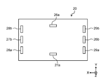
- FIG. 9 is a plan view schematically showing an example of the arrangement of connectors provided on the light source board 20 in the image display device 1 according to the second embodiment.
- substrate 20 is shown.
- the light source board 20 includes a signal input connector 26a, a signal input connector 26b, a signal output connector 27a, a signal output connector 27b, a power input connector 28a, a power input connector 28b, a power output connector 29a, and a power output.
- Connector 29b These connectors are respectively arranged at different positions on the back surface of the light source substrate 20.
- the connector is a terminal (so-called land pattern) on the light source board 20 for enabling electrical connection with a cable.
- a cable may be directly connected to the connector, and a socket or a receptacle for receiving the cable may be attached, and the cable may be connected via the socket or the receptacle.
- the connector to which a cable is connected can be selected appropriately. Therefore, when the light source boards 20 arranged at different positions are compared with each other, there are cases where a cable is connected to a connector at the same position of each light source board 20 and a cable is not connected.
- the light source board 20 distributes the control signal input to the signal input connector 26a from the signal processing board 92 or another light source board 20 to the driver elements mounted on the light source board 20, and the signal output connector 27a and the signal output. It has wiring (not shown) provided to output to both connectors 27b (hereinafter also referred to as “through output”).
- the light source board 20 has a wiring formed so as to distribute the control signal input to the signal input connector 26b to the driver elements mounted on the light source board 20 and to output the control signal through the signal output connector 27b ( Not shown).
- the light source board 20 passes through both the signal output connector 27a and the signal output connector 27b. Is output. Further, when a control signal is input to the light source board 20 to the signal input connector 26b, the control signal is output through from the signal output connector 27b.
- the control signal is a signal related to luminance for causing each LED 21 to emit light with luminance based on the brightness of the image in the corresponding region 71.
- each of the plurality of LEDs 21 is driven (dimmed) by the driver element 22 and the driver element 23 so as to emit light with luminance according to the control signal.
- the light source board 20 distributes the power input from the power supply board 93 or another light source board 20 to the power input connector 28a or the power input connector 28b to each element mounted on the light source board 20, and outputs power.
- the connector 29a and the power output connector 29b have wiring provided to output through (not shown).
- the light source board 20 receives the power from the power output connector 29a and the power output connector. Through output from both terminals 29b. In each light source board
- the light source board 20 shown in Embodiment 2 has a plurality of connectors for distributing signals or power at different positions. Therefore, in the image display device 1 shown in the second embodiment, in the light source substrate 20, for example, other usable connectors are used while avoiding connectors that cannot be used because other members are arranged. A connector can be appropriately selected and used according to the arrangement position or the like. Therefore, in this image display device 1, for example, when a plurality of light source substrates 20 are attached to the base plate 10, a plurality of light source substrates 20 having the same configuration are used even if the usable connectors differ depending on the attachment positions. be able to. Thereby, in the image display device 1 shown in the second embodiment, it is possible to reduce the cost by using a plurality of light source substrates 20 having the same configuration (that is, by sharing the substrates).
- Such a configuration shown in the second embodiment is suitable, for example, when a backlight is configured by electrically connecting (cascading) a plurality of light source substrates 20 to each other.
- FIG. 10 is a plan view schematically showing an example of connection of a plurality of light source substrates 20 constituting a backlight in the image display device 1 according to the second embodiment.
- FIG. 10 shows a plan view of the back side of the base plate 10 to which 16 light source substrates 20 are attached as an example. Since the light source board
- the plurality of light source substrates 20 included in the image display device 1 are arranged in a matrix on the base plate 10.
- the plurality of light source boards 20 are electrically connected (cascade connected) to each other by a cable 14 or a cable 15 as shown in FIG.
- the base plate 10 is provided with a reinforcing beam 11 at the upper end of the back surface and a reinforcing beam 12 at the lower end of the back surface.
- a predetermined connector of the light source board 20 can be electrically connected to the base plate 10 to another board (the signal processing board 92, the power supply board 93, or the other light source board 20) via a cable.
- a plurality of openings 13 are provided.
- the reinforcing beam 11 is provided at substantially the same position as a predetermined one of the plurality of openings 13 provided in the base plate 10, and a predetermined connector of one light source substrate 20 (for example, the light source substrate 20a).
- An opening 13a is provided for allowing the signal input connector 26a (for example, the signal input connector 26a) to be electrically connected to another substrate (for example, the signal processing substrate 92) via a cable.
- substrate 20 is exposed to the back surface side of the baseplate 10 through the opening 13 provided in the baseplate 10, or the opening 13a provided in the opening 13 and the reinforcement beam 11. FIG. ing. Thereby, each light source board
- the 16 light source boards 20 are electrically connected to each other by the cable 14 and the cable 15 to constitute a backlight.
- reference numerals 20a to 20g are given to the seven light source substrates 20 in the upper two rows.
- the signal output connector 27b of each light source board 20 is electrically connected to the signal input connector 26b of the light source board 20 on the left side in the drawing by the cable 14.
- the signal output connector 27a of each light source board 20 is electrically connected to the signal input connector 26a of the light source board 20 directly under the drawing by the cable 14.
- the signal input connector 26a of the light source board 20a at the upper right end in the drawing is electrically connected to the signal processing board 92 by a cable.
- the control signal supplied from the signal processing board 92 is input to the signal input connector 26a of the light source board 20a.
- This control signal is output through to the signal output connector 27a and the signal output connector 27b of the light source board 20a, and is input to the signal input connector 26a of the light source board 20c and the signal input connector 26b of the light source board 20b via the cable 14, respectively. Is done.
- the control signal is distributed from one light source board 20 to another light source board 20 through the cable 14.
- the control signal supplied from the signal processing board 92 is distributed to all the light source boards 20 included in the image display device 1.
- the path through which the control signal is distributed is indicated by a one-dot chain line.
- the power supplied from the power supply board 93 is input to the four light source boards 20 arranged at the left end in FIG.
- the power input connector 28b and the power output connector 29b cannot be used due to the reinforcing beam 11. Therefore, the power supplied from the power supply board 93 avoids the power input connector 28b that cannot be used by the reinforcing beam 11 for the light source board 20d arranged at the uppermost of the four arranged at the left end.
- the other three light source boards 20 including the light source board 20e are input to the power input connector 28b.
- This power is transmitted through the power output connector 29a while avoiding the power output connector 29b that cannot be used by the reinforcing beam 11 in the light source board 20d, and the power of the light source board 20f arranged on the right side in the drawing via the cable 15 It is input to the input connector 28a.
- power is output through to the power output connector 29b, and the power input connector of the light source board 20 arranged on the right side in the drawing via the cable 15 28b.
- electric power is distributed from one light source substrate 20 to another light source substrate 20.
- the power supplied from the power supply substrate 93 is distributed to all the light source substrates 20 included in the image display device 1.
- a path through which power is distributed is indicated by a two-dot chain line.
- the light source substrate 20 included in the image display device 1 operates in accordance with the control signal and power distributed in this manner, and each of the plurality of LEDs 21 is driven (adjusted) so as to emit light with luminance according to the distributed control signal. Light).
- the plurality of light source substrates 20 are electrically connected (cascade connection) to each other, so that the number of cables necessary for connection can be reduced.
- the light source board 20 by providing a plurality of connectors for distributing signals or power at different positions, for example, a connector that cannot be used because other members (for example, the reinforcing beam 11) are arranged can be avoided. It is possible to select and use the connector appropriately according to the arrangement position of the member, such as using another usable connector.
- the image display device in an image display device having a plurality of LEDs that can be dimmed independently, the image display device can be reduced in size, thickness, and assembly cost can be reduced.
- Embodiment 3 Next, Embodiment 3 will be described with reference to FIGS.
- the image display device 1 (not shown) shown in the third embodiment is substantially the same as the image display device 1 shown in the first or second embodiment.
- the light source substrate 20 is provided with a configuration suitable for heat management.
- This structure is characterized by the arrangement of the conductive foil provided on the light source substrate 20.
- the conductor foil is a conductor provided with a metal thin film or the like on the substrate in order to supply electric power, ground or a signal to each element on the light source substrate 20.
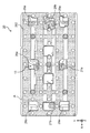
- FIG. 11 is a plan view schematically showing an example of the first conductor foil disposed on the first main surface of the light source substrate 20 included in the image display device 1 according to the third embodiment.
- the first main surface is a surface on which the LED 21, the driver element 22, and the driver element 23 are mounted.
- a power pattern foil 201 and a signal pattern foil 203 are disposed on the first main surface.
- the power supply pattern foil 201 and the signal pattern foil 203 are examples of conductor foils.
- the power supply pattern foil 201 is arranged in the area shown in gray
- the signal pattern foil 203 is arranged in a part of the area shown in white.
- a ground pattern foil may be further disposed on the first main surface.
- the conductor foils (for example, the power pattern foil 201, the signal pattern foil 203, etc.) arranged on the first main surface are collectively referred to as a first conductor foil.
- the power input connector 28a, the power input connector 28b, the power output connector 29a, and the power output connector 29b are a plurality of power supply connectors that are electrically connected to different positions of the first conductor foil (power supply pattern foil 201). It is an example.
- the surface on the opposite side of the 1st main surface in the light source substrate 20 is called 2nd main surface.
- the ground is a ground potential or a reference potential.
- FIG. 12 is a plan view schematically showing an example of the second conductor foil disposed on the second main surface of the light source substrate 20 included in the image display device 1 according to the third embodiment.
- the ground pattern foil 202 is disposed on the second main surface.
- the ground pattern foil 202 is an example of a conductor foil. In the example shown in FIG. 12, the ground pattern foil 202 is arranged in a region indicated by gray. A signal pattern foil may be further disposed on the second main surface.
- the conductor foil (for example, the ground pattern foil 202 etc.) arrange
- the 1st conductor foil and the 2nd conductor foil are provided so that an area may become substantially equal mutually. That is, in the light source substrate 20 in the present embodiment, the area of the first conductor foil and the area of the second conductor foil are substantially equal to each other. Note that “substantially equal” means that the difference between the area of the first conductor foil and the area of the second conductor foil is set in a range in which the substrate is not substantially warped during mounting. . Since this setting range varies depending on the material, size, thickness, etc. of the substrate, it is desirable to set it appropriately.
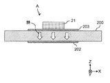
- FIG. 13 is a cross-sectional view schematically showing an example of the structure of the light source substrate 20 included in the image display device 1 according to the third embodiment.
- FIG. 13 shows an example of a cross-sectional structure of the region A (the region indicated by the broken-line circle in FIG. 11).
- the region A is a region including the LEDs 21 when the light source substrate 20 is viewed in plan (for example, when the first main surface of the light source substrate 20 is viewed from a direction perpendicular to the first main surface). is there.
- the upper surface of the substrate 200 corresponds to the first main surface of the light source substrate 20, and the lower surface of the substrate 200 corresponds to the second main surface of the light source substrate 20.
- the signal pattern foil 203 is formed on the first main surface (the upper surface of the base body 200) of the light source substrate 20.
- Ground pattern foils 202 are respectively disposed on the second main surface (the lower surface of the base body 200). That is, the ground pattern foil 202 is disposed in at least a region corresponding to the LED 21 on the second main surface.
- a ground pattern foil (not shown) may be further arranged on the first main surface of the light source substrate 20, and the LED 21 is driven by the current supplied through the signal pattern foil 203 and the ground pattern foil. May be. Such a structure is applied to each region including the LEDs 21 in the light source substrate 20.
- the base 200 is made of a resin material such as glass epoxy, and the power pattern foil 201, the ground pattern foil 202, and the signal pattern foil 203 are made of a metal material containing copper. May be.
- the LED 21 may be soldered to the signal pattern foil 203 and the ground pattern foil (not shown) on the first main surface of the light source substrate 20.
- the present embodiment is not limited to those configurations.
- the ground pattern foil 202 is arranged directly below the LED 21 (directly below in FIG. 13, that is, the region corresponding to the LED 21 on the second main surface). In comparison, the heat of the LED 21 can be efficiently released to the outside.
- the light source substrate 20 by providing the power pattern foil 201 on the first main surface widely, not only the warpage of the substrate is suppressed but also the effect of improving the power efficiency and suppressing the heat generation can be obtained.
- the suppression effect of the heat generation will be described.
- the image display device 1 a plurality (four in the example shown in FIG. 10) of light source boards 20 are connected in series by a cable 15.
- the operating power of the light source board 20 is distributed from the power supply board 93 to each light source board 20 through the connection.
- the power line is mainly formed by the power pattern foil 201 on the first main surface of the light source substrate 20, and the ground line is mainly formed by the ground pattern foil 202 on the second main surface of the light source substrate 20.
- FIG. 14 is a conceptual diagram illustrating an example of a power supply line formed by the power supply pattern foil 201 in the light source substrate 20 included in the image display device 1 according to the third embodiment.
- FIG. 14 equivalently shows an example of a power line formed by a relatively wide power pattern foil 201 in the light source substrate 20 having a relatively wide ground pattern foil 202 for heat dissipation.
- the gray part represents an equivalent power line.
- FIG. 15 shows a comparative example with respect to FIG.
- FIG. 15 is a conceptual diagram showing an example of a power supply line formed by the power supply pattern foil 211 in the light source substrate 210 in the comparative example.
- FIG. 15 does not employ a configuration in which a wide ground pattern foil is provided for heat dissipation (that is, a light source substrate 210 having a relatively narrow ground pattern foil).
- An example of the power line is shown equivalently.
- the gray part represents an equivalent power line.
- the light source substrate 20 is provided with a wide ground pattern foil 202 for heat dissipation. And in order to suppress the curvature of a board
- the light source substrate 20 is screwed to the base plate 10 by screws passing through the screw holes 25.
- This screw is made of metal and functions as an electrical conductor.
- This screw is an example of a metal fastening member.
- the base plate 10 is also made of metal. Accordingly, by forming the screw hole 25 so that the ground pattern foil 202 and the screw are electrically connected, the ground pattern foil 202 is electrically connected to the base plate 10 via the screw. Thereby, the base plate 10 is used as a rigid base for holding the light source substrate 20 and also functions as a part of the ground line.
- the base plate 10 having a relatively small electrical resistance hereinafter simply referred to as resistance
- the area of the ground pattern foil necessary for power distribution in the light source substrate 20 can be reduced. it can.
- the area of a power supply pattern foil can be expanded because the area of a ground pattern foil is reduced. In such a configuration, the width of the power supply line (power supply pattern foil 201) shown in FIG. 14 can be further increased.
- the resistance of the power line formed of the large-area power pattern foil 201 and the ground line using the base plate 10 are relatively small. Therefore, in light source substrate 20 shown in the present embodiment, a voltage drop that occurs when power is distributed can be reduced, and heat generation in driver element 22 and driver element 23 can be suppressed. Details will be described with reference to FIG.
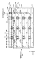
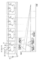
- FIG. 16 is a diagram for explaining a heat generation suppressing effect by the light source substrate 20 included in the image display device 1 according to the third embodiment.
- FIG. 16 is a circuit diagram showing an example of an equivalent circuit for distributing electric power in the light source substrate 20.
- the power supply line of the light source substrate 20 is represented by a resistor R
- the base plate 10 as a ground line is represented by a white bar.
- FIG. 16 is a graph schematically showing an example of a power supply voltage in consideration of a voltage drop generated in the power supply line (resistor R).
- the voltage drop in the light source substrate 210 (see FIG. 15) having a relatively large resistance R is indicated by a broken line, and the resistance R is relatively small ( That is, the state of the voltage drop in the light source substrate 20 (see FIG. 14) having a relatively wide power supply line is shown by a solid line.
- the light source substrate 210 having a relatively large resistance R In order to maintain the power supply voltage at the final-stage light source substrate 20 (or 210) (the rightmost light source substrate in the drawing) at a predetermined voltage value, as shown in the graph, the light source substrate 210 having a relatively large resistance R.
- the initial value of the power supply voltage (the voltage at the left end of the graph.
- the power supply voltage generated in the power supply board 93 is used to compensate for the voltage drop in the power supply line. ) Needs to be relatively high.
- the heat loss in the driver element 22 and the driver element 23 is relatively small as shown in FIG. Is done.
- the driver element 22 is a transistor that controls the operating current of the LED 21 by converting the difference between the power supply voltage and the voltage for driving the LED 21 into heat by the on-resistance of the driver element 22 itself. By being reduced, heat generation can be greatly suppressed.
- 90% or more of the first conductor foil provided on the first main surface of the light source substrate 20 may be used as the power supply pattern foil 201 in terms of area ratio.
- the voltage drop in the power supply line is further reduced, and the initial value of the power supply voltage can be further reduced.
- the initial value of the power supply voltage it is possible to further suppress heat generation (heat loss) in the driver element 22 and the driver element 23 (particularly the driver element 22).
- the image display device includes a liquid crystal display panel and a light source substrate for illuminating the liquid crystal display panel from the back.
- the light source substrate includes a plurality of light emitting diodes each provided corresponding to a different area of the liquid crystal display panel, and each of the plurality of light emitting diodes has a luminance according to the brightness in the corresponding area of the image according to the control signal
- a driver element that is driven by A first conductor foil is disposed on the first main surface on which the light emitting diodes of the light source substrate are mounted, and a second conductor foil is disposed on the second main surface opposite to the first main surface.
- a ground pattern foil is disposed as a second conductor foil in a region including each of the plurality of light emitting diodes in plan view on the second main surface.
- the area of the first conductor foil and the area of the second conductor foil are substantially equal to each other.
- the image display device includes a liquid crystal display panel, a metal base plate, and a light source substrate that is fixed to the base plate and illuminates the liquid crystal display panel from the back.
- the light source substrate includes a plurality of light emitting diodes each provided corresponding to a different area of the liquid crystal display panel, and each of the plurality of light emitting diodes has a luminance according to the brightness in the corresponding area of the image according to the control signal
- a driver element that is driven by A first conductor foil is disposed on the first main surface on which the light emitting diodes of the light source substrate are mounted, and a second conductor foil is disposed on the second main surface opposite to the first main surface. At least a portion of the second conductor foil is a ground pattern foil that is electrically connected to the base plate.
- the image display device 1 is an example of an image display device.
- the liquid crystal display panel 70 is an example of a liquid crystal display panel.
- Each of the light source substrate 20 and the light source substrates 20a to 20g is an example of a light source substrate.
- the LED 21 is an example of a light emitting diode.
- the driver element 22 and the driver element 23 are examples of driver elements.
- Region A is an example of a region including a light emitting diode.
- the ground pattern foil 202 is an example of a ground pattern foil.
- the base plate 10 is an example of a base plate.
- the image display device 1 includes a liquid crystal display panel 70 and a light source substrate 20 for illuminating the liquid crystal display panel 70 from the back.
- the light source substrate 20 includes a plurality of LEDs 21 provided corresponding to different regions of the liquid crystal display panel 70, and a plurality of LEDs 21 each having a luminance corresponding to the brightness in the corresponding region of the image according to the control signal.
- a driver element 22 and a driver element 23 to be driven are mounted.
- a first conductor foil is disposed on the first main surface of the light source substrate 20 on which the LEDs 21 are mounted, and a second conductor foil is disposed on the second main surface opposite to the first main surface.
- a ground pattern foil 202 is disposed as a second conductor foil in a region including each of the plurality of LEDs 21 in plan view on the second main surface. The area of the first conductor foil and the area of the second conductor foil are substantially equal to each other.
- the image display device 1 includes a liquid crystal display panel 70, a metal base plate 10, and a light source substrate 20 that is fixed to the base plate 10 and illuminates the liquid crystal display panel 70 from the back.
- the light source substrate 20 includes a plurality of LEDs 21 provided corresponding to different regions of the liquid crystal display panel 70, and a plurality of LEDs 21 each having a luminance corresponding to the brightness in the corresponding region of the image according to the control signal.
- a driver element 22 and a driver element 23 to be driven are mounted.
- a first conductor foil is disposed on the first main surface of the light source substrate 20 on which the LEDs 21 are mounted, and a second conductor foil is disposed on the second main surface opposite to the first main surface. At least a part of the second conductor foil is a ground pattern foil 202 that is electrically connected to the base plate 10.
- 90% or more of the first conductor foil may be the power pattern foil in the area ratio.
- the light source substrate may be fixed to the base plate with a metal fastening member, and the ground pattern foil may be electrically connected to the base plate via the fastening member.
- the screw that screws the light source substrate 20 to the base plate 10 through the screw hole 25 is an example of a metal fastening member.
- the light source substrate may have a plurality of power connectors that are electrically connected to different positions of the first conductor foil.
- the power input connector 28a, the power input connector 28b, the power output connector 29a, and the power output connector 29b are examples of a plurality of power connectors.
- a ground pattern foil may be disposed as a second conductor foil in a region of the second main surface including each of the plurality of light emitting diodes in plan view.
- the area of the first conductor foil and the area of the second conductor foil may be substantially equal to each other.
- the driver element may be mounted on the first main surface.
- the light source substrate 20 uses a power supply line formed of a large-area power supply pattern foil 201 and / or a ground line using the base plate 10 or both. Since the initial value can be made relatively low, the heat generation of the driver element 22 and the driver element 23 can be suppressed.
- 90% or more of the first conductor foil provided on the first main surface of the light source substrate 20 may be used as the power supply pattern foil in terms of area ratio.
- the voltage drop in the power supply line is further reduced, and the LED 21 can be driven with a lower power supply voltage.
- fever (heat loss) in the driver element 22 and the driver element 23 can be suppressed by reduction of a power supply voltage.
- Embodiments 1 to 3 As described above, Embodiments 1 to 3 have been described as examples of the technology disclosed in the present application. For this purpose, the accompanying drawings and detailed description are provided.
- the present disclosure is applicable to an image display device. Specifically, the present disclosure is applicable to a television receiver, a video recording / playback apparatus, a computer display apparatus, or the like.
Landscapes
- Engineering & Computer Science (AREA)
- Physics & Mathematics (AREA)
- General Physics & Mathematics (AREA)
- Nonlinear Science (AREA)
- Theoretical Computer Science (AREA)
- General Engineering & Computer Science (AREA)
- Chemical & Material Sciences (AREA)
- Crystallography & Structural Chemistry (AREA)
- Computer Hardware Design (AREA)
- Microelectronics & Electronic Packaging (AREA)
- Optics & Photonics (AREA)
- Mathematical Physics (AREA)
- Planar Illumination Modules (AREA)
- Liquid Crystal (AREA)
- Arrangement Of Elements, Cooling, Sealing, Or The Like Of Lighting Devices (AREA)
- Devices For Indicating Variable Information By Combining Individual Elements (AREA)
- Fastening Of Light Sources Or Lamp Holders (AREA)
Abstract
Description
以下、図1~図8を参照しながら実施の形態1における画像表示装置1について説明する。なお、本実施の形態では、図面にX軸、Y軸、Z軸の3軸を示し、液晶表示パネルの長辺に平行な方向の軸をX軸、液晶表示パネルの短辺に平行な方向の軸をY軸、X軸Y軸の双方に直交する軸をZ軸とする。しかし、これらの軸は便宜的に示したものに過ぎず、何ら本開示を限定するものではない。
実施の形態1における画像表示装置1は、液晶表示パネルと、その液晶表示パネルを背面から照明するための光源基板と、を備える。画像表示装置1は、画像表示装置の一例である。光源基板には、各々が液晶表示パネルの互いに異なる領域に対応して設けられた複数のLEDと、複数のLEDの各々を、制御信号に従って画像の対応領域内の明るさに応じた輝度で発光するように駆動(調光)するドライバ素子と、が搭載される。なお、画像の対応領域内の明るさとは、1つのLED(または、一箇所に配置されたLED)が照明する液晶表示パネルの領域(すなわち、そのLEDに対応する領域)における画像の明るさ(画像の部分的な明るさ)のことである。
以上のように構成された画像表示装置1では、次のような効果が得られる。
次に、図9および図10を参照しながら、実施の形態2について説明する。
実施の形態2には、他の基板との電気的な接続をケーブルを介して行う構成を光源基板20に設けた画像表示装置1を開示する。実施の形態2では、実施の形態1の画像表示装置1の構成に加えて、適切なコネクタを選択してケーブルを接続できる構成を光源基板20が備えている。
以上のように構成された画像表示装置1では、複数の光源基板20を互いに電気的に連結(カスケード接続)することにより、接続に必要なケーブルを削減することができる。
次に、図11~図16を参照しながら、実施の形態3について説明する。
図11は、実施の形態3における画像表示装置1が備える光源基板20の第1主面に配置された第1導体箔の一例を模式的に示す平面図である。
以上のように、本実施の形態において、画像表示装置は、液晶表示パネルと、液晶表示パネルを背面から照明するための光源基板と、を備える。光源基板には、各々が液晶表示パネルの互いに異なる領域に対応して設けられた複数の発光ダイオードと、複数の発光ダイオードの各々を、制御信号に従って画像の対応領域内の明るさに応じた輝度で駆動するドライバ素子と、が搭載される。光源基板の発光ダイオードが搭載された第1主面には第1導体箔が配置され、第1主面の反対側の第2主面には第2導体箔が配置される。第2主面の、平面視で複数の発光ダイオードの各々を含む領域には、第2導体箔として、グランドパターン箔が配置される。そして、第1導体箔の面積と第2導体箔の面積とは互いに略等しい。
以上のように、本出願において開示する技術の例示として、実施の形態1~3を説明した。そのために、添付図面および詳細な説明を提供した。
1a 筐体
10 ベースプレート
11,12 補強梁
13,13a 開口
14,15 ケーブル
20,20a,20b,20c,20d,20e,20f,20g,210 光源基板
21 LED
22,23 ドライバ素子
24 開口
25 ビス孔
26a,26b 信号入力コネクタ
27a,27b 信号出力コネクタ
28a,28b 電力入力コネクタ
29a,29b 電力出力コネクタ
30 反射シート
31 隆起
32,33 開口
35 接着テープ
36 サポートピン
40 フラッタ
41,41A 孔
50 光学シート
60 モールドフレーム
70 液晶表示パネル
71 領域
80 ベゼル
91 接続端子基板
92 信号処理基板
93 電源基板
200 基体
201,211 電源パターン箔
202 グランドパターン箔
203 信号パターン箔
Claims (8)
- 液晶表示パネルと、
前記液晶表示パネルを背面から照明するための光源基板と、を備え、
前記光源基板に、
各々が前記液晶表示パネルの互いに異なる領域に対応して設けられた複数の発光ダイオードと、
前記複数の発光ダイオードの各々を、制御信号に従って画像の対応領域内の明るさに応じた輝度で駆動するドライバ素子と、
が搭載され、
前記光源基板の前記発光ダイオードが搭載された第1主面に第1導体箔が配置され、前記第1主面の反対側の第2主面に第2導体箔が配置され、
前記第2主面の、平面視で前記複数の発光ダイオードの各々を含む領域に、前記第2導体箔として、グランドパターン箔が配置され、
前記第1導体箔の面積と前記第2導体箔の面積とが略等しい、
画像表示装置。 - 液晶表示パネルと、
金属製のベースプレートと、
前記ベースプレートに固定され、前記液晶表示パネルを背面から照明するための光源基板と、を備え、
前記光源基板に、
各々が前記液晶表示パネルの互いに異なる領域に対応して設けられた複数の発光ダイオードと、
前記複数の発光ダイオードの各々を、制御信号に従って画像の対応領域内の明るさに応じた輝度で駆動するドライバ素子と、
が搭載され、
前記光源基板の前記発光ダイオードが搭載された第1主面に第1導体箔が配置され、前記第1主面の反対側の第2主面に第2導体箔が配置され、
前記第2導体箔の少なくとも一部は、前記ベースプレートに電気的に接続されたグランドパターン箔である、
画像表示装置。 - 面積比で前記第1導体箔の90%以上が電源パターン箔である、
請求項2に記載の画像表示装置。 - 前記光源基板は、金属製の締結部材にて前記ベースプレートに固定されており、
前記グランドパターン箔は、前記締結部材を介して前記ベースプレートに電気的に接続されている、
請求項2に記載の画像表示装置。 - 前記光源基板は、前記第1導体箔の異なる位置に接続された複数の電源コネクタを有している、
請求項2に記載の画像表示装置。 - 前記第2主面の、平面視で前記複数の発光ダイオードの各々を含む領域に、前記第2導体箔として、グランドパターン箔が配置され、
前記第1導体箔の面積と前記第2導体箔の面積とが略等しい、
請求項2に記載の画像表示装置。 - 前記ドライバ素子が前記第1主面に搭載されている、
請求項1に記載の画像表示装置。 - 前記ドライバ素子が前記第1主面に搭載されている、
請求項2に記載の画像表示装置。
Priority Applications (3)
| Application Number | Priority Date | Filing Date | Title |
|---|---|---|---|
| EP16841119.7A EP3346320B1 (en) | 2015-09-01 | 2016-08-30 | Video display device |
| US15/754,208 US10663793B2 (en) | 2015-09-01 | 2016-08-30 | Image display device |
| JP2017537547A JP6646816B2 (ja) | 2015-09-01 | 2016-08-30 | 画像表示装置 |
Applications Claiming Priority (4)
| Application Number | Priority Date | Filing Date | Title |
|---|---|---|---|
| JP2015-172363 | 2015-09-01 | ||
| JP2015172363 | 2015-09-01 | ||
| JP2016047073 | 2016-03-10 | ||
| JP2016-047073 | 2016-03-10 |
Publications (1)
| Publication Number | Publication Date |
|---|---|
| WO2017038085A1 true WO2017038085A1 (ja) | 2017-03-09 |
Family
ID=58187037
Family Applications (1)
| Application Number | Title | Priority Date | Filing Date |
|---|---|---|---|
| PCT/JP2016/003945 Ceased WO2017038085A1 (ja) | 2015-09-01 | 2016-08-30 | 画像表示装置 |
Country Status (4)
| Country | Link |
|---|---|
| US (1) | US10663793B2 (ja) |
| EP (1) | EP3346320B1 (ja) |
| JP (1) | JP6646816B2 (ja) |
| WO (1) | WO2017038085A1 (ja) |
Cited By (1)
| Publication number | Priority date | Publication date | Assignee | Title |
|---|---|---|---|---|
| WO2025178118A1 (ja) * | 2024-02-22 | 2025-08-28 | ミネベアミツミ株式会社 | 面状照明装置 |
Families Citing this family (9)
| Publication number | Priority date | Publication date | Assignee | Title |
|---|---|---|---|---|
| JP6695035B2 (ja) * | 2015-07-01 | 2020-05-20 | パナソニックIpマネジメント株式会社 | バックライト装置および液晶表示装置 |
| CN107390428A (zh) * | 2017-07-24 | 2017-11-24 | 武汉华星光电技术有限公司 | 直下式背光模组以及液晶显示器 |
| CN112955813B (zh) * | 2019-07-29 | 2023-04-07 | 京东方科技集团股份有限公司 | 绑定背板及其制作方法、背光模组及显示装置 |
| TWI743533B (zh) * | 2019-08-14 | 2021-10-21 | 佳世達科技股份有限公司 | 顯示裝置及其框架模組 |
| JP7231832B2 (ja) | 2019-12-27 | 2023-03-02 | 日亜化学工業株式会社 | 発光装置、液晶表示装置 |
| US11562702B2 (en) * | 2020-03-31 | 2023-01-24 | Sharp Kabushiki Kaisha | Dimming unit, and liquid crystal display device |
| US11428987B2 (en) * | 2020-05-22 | 2022-08-30 | Apple Inc. | Electronic device display with a backlight having light-emitting diodes and driver integrated circuits in an active area |
| KR102827323B1 (ko) * | 2021-02-26 | 2025-07-02 | 삼성디스플레이 주식회사 | 표시 장치 및 그 구동 방법 |
| CN116936537A (zh) * | 2022-04-01 | 2023-10-24 | 群创光电股份有限公司 | 电子装置 |
Citations (2)
| Publication number | Priority date | Publication date | Assignee | Title |
|---|---|---|---|---|
| JP2012119436A (ja) * | 2010-11-30 | 2012-06-21 | Stanley Electric Co Ltd | Led線状光源およびバックライト |
| JP2013182076A (ja) * | 2012-02-29 | 2013-09-12 | Toshiba Corp | 映像表示装置および発光装置 |
Family Cites Families (55)
| Publication number | Priority date | Publication date | Assignee | Title |
|---|---|---|---|---|
| JP3342665B2 (ja) | 1998-06-17 | 2002-11-11 | 株式会社カスト | 表示装置 |
| JP2001338505A (ja) | 2000-05-26 | 2001-12-07 | Matsushita Electric Works Ltd | 照明装置 |
| JP4067802B2 (ja) | 2001-09-18 | 2008-03-26 | 松下電器産業株式会社 | 照明装置 |
| KR100942140B1 (ko) | 2002-12-26 | 2010-02-16 | 엘지디스플레이 주식회사 | 액정표시모듈 및 그 조립방법 |
| TW200426412A (en) | 2003-05-29 | 2004-12-01 | Au Optronics Corp | Vertical type backlight unit |
| JP2005109228A (ja) * | 2003-09-30 | 2005-04-21 | Toshiba Lighting & Technology Corp | Led装置およびled照明装置 |
| JP2005339881A (ja) | 2004-05-25 | 2005-12-08 | Hitachi Displays Ltd | 照明装置、照明モジュール及び液晶表示装置 |
| KR101157233B1 (ko) | 2004-10-30 | 2012-06-15 | 엘지디스플레이 주식회사 | 발광 다이오드 백라이트 장치 및 이를 채용한 액정표시장치 |
| JP4280283B2 (ja) | 2006-01-27 | 2009-06-17 | 株式会社オプトデザイン | 面照明光源装置及びこれを用いた面照明装置 |
| KR100755615B1 (ko) | 2006-04-14 | 2007-09-06 | 삼성전기주식회사 | 발광 다이오드를 이용한 액정 표시 장치의 백라이트 |
| JP4821442B2 (ja) | 2006-05-31 | 2011-11-24 | ソニー株式会社 | バックライト装置及び液晶表示装置 |
| JP4151717B2 (ja) * | 2006-07-21 | 2008-09-17 | ソニー株式会社 | 光源モジュール、光源装置及び液晶表示装置 |
| JP2008166304A (ja) | 2006-12-26 | 2008-07-17 | Sony Corp | バックライト装置及び液晶表示装置 |
| JP2008270144A (ja) | 2007-03-22 | 2008-11-06 | Furukawa Electric Co Ltd:The | ライトボックス |
| KR100872696B1 (ko) | 2007-04-16 | 2008-12-10 | 엘지이노텍 주식회사 | 광원 장치 및 이를 이용한 디스플레이 장치 |
| WO2008156020A1 (ja) | 2007-06-19 | 2008-12-24 | Sharp Kabushiki Kaisha | 基板及び照明装置 |
| KR100951274B1 (ko) | 2007-07-19 | 2010-05-06 | 삼성엘이디 주식회사 | 백라이트 유닛 |
| US7905618B2 (en) | 2007-07-19 | 2011-03-15 | Samsung Led Co., Ltd. | Backlight unit |
| JP4796016B2 (ja) | 2007-07-27 | 2011-10-19 | シャープ株式会社 | バックライト装置および液晶表示装置 |
| KR101410496B1 (ko) | 2007-11-08 | 2014-06-20 | 삼성디스플레이 주식회사 | 광원모듈, 이를 갖는 백라이트 어셈블리 및 이를 갖는표시장치 |
| JP4968014B2 (ja) | 2007-11-22 | 2012-07-04 | ソニー株式会社 | バックライト装置及び液晶表示装置 |
| JP4926928B2 (ja) | 2007-12-05 | 2012-05-09 | シャープ株式会社 | 照明装置および液晶表示装置 |
| JP5320738B2 (ja) | 2007-12-28 | 2013-10-23 | ソニー株式会社 | 発光制御システムおよび画像表示システム |
| US20090201441A1 (en) | 2008-02-13 | 2009-08-13 | Rohm And Haas Electronic Materials Llc | Tensioned optical element having crimping frame and spring |
| KR101519331B1 (ko) | 2008-02-18 | 2015-05-13 | 삼성디스플레이 주식회사 | 백라이트 어셈블리 및 이를 갖는 표시장치 |
| JP2009222793A (ja) | 2008-03-13 | 2009-10-01 | Hitachi Ulsi Systems Co Ltd | 液晶表示装置 |
| KR101442006B1 (ko) | 2008-06-05 | 2014-09-19 | 삼성디스플레이 주식회사 | 백라이트 어셈블리 및 이를 갖는 표시장치 |
| KR101494849B1 (ko) * | 2008-06-13 | 2015-02-24 | 삼성디스플레이 주식회사 | 백라이트 어셈블리 및 이를 포함하는 표시 장치 |
| JP4968219B2 (ja) | 2008-09-18 | 2012-07-04 | 株式会社Jvcケンウッド | 液晶表示装置及びこれに用いる映像表示方法 |
| US20100109562A1 (en) | 2008-11-06 | 2010-05-06 | StarChips Technology Inc. | Backlight module and light-emitting device thereof |
| KR101812563B1 (ko) | 2008-12-19 | 2017-12-27 | 가부시키가이샤 한도오따이 에네루기 켄큐쇼 | 전자기기 |
| WO2010101062A1 (ja) | 2009-03-05 | 2010-09-10 | シャープ株式会社 | 発光モジュール、発光モジュールユニット及びバックライトシステム |
| JP4519944B1 (ja) | 2009-05-22 | 2010-08-04 | シャープ株式会社 | 光源装置及び表示装置 |
| JP5351723B2 (ja) | 2009-05-22 | 2013-11-27 | シャープ株式会社 | 光源装置及び表示装置 |
| KR101352276B1 (ko) * | 2009-07-24 | 2014-01-16 | 엘지디스플레이 주식회사 | 발광다이오드의 방열장치와 이를 이용한 액정표시장치 |
| JP4910023B2 (ja) | 2009-08-27 | 2012-04-04 | シャープ株式会社 | 光源装置 |
| BR112012004586A2 (pt) | 2009-08-31 | 2016-04-05 | Sharp Kk | aprelho de iluminação e aparelho de exibição |
| JP5619406B2 (ja) | 2009-10-23 | 2014-11-05 | 積水化成品工業株式会社 | 照明体 |
| JP4820454B2 (ja) * | 2009-10-23 | 2011-11-24 | シャープ株式会社 | 液晶表示装置及びテレビ受信装置 |
| WO2011055565A1 (ja) | 2009-11-06 | 2011-05-12 | シャープ株式会社 | 照明装置、表示装置、及びテレビジョン受像器 |
| EP2489928A4 (en) | 2009-11-12 | 2014-03-12 | Sharp Kk | LIGHTING DEVICE, DISPLAY DEVICE, AND TELEVISION STATION |
| JP5258978B2 (ja) * | 2010-01-12 | 2013-08-07 | シャープ株式会社 | Led基板、バックライトユニットおよび液晶表示装置 |
| US20110304798A1 (en) | 2010-06-10 | 2011-12-15 | Sharp Kabushiki Kaisha | Illumination device and liquid crystal display device |
| JP2012004067A (ja) | 2010-06-21 | 2012-01-05 | Harison Toshiba Lighting Corp | 面照明装置 |
| WO2011162016A1 (ja) | 2010-06-25 | 2011-12-29 | シャープ株式会社 | Ledバックライト装置および液晶表示装置 |
| US20120019490A1 (en) | 2010-07-23 | 2012-01-26 | Hsien-Jung Huang | Modular led display structure with connecting edge banding to connect each other |
| JP2012174634A (ja) | 2011-02-24 | 2012-09-10 | Sharp Corp | 光源モジュールおよび光学部材 |
| JP2012204337A (ja) | 2011-03-28 | 2012-10-22 | Sharp Corp | 照明装置および表示装置 |
| JP2012212509A (ja) | 2011-03-30 | 2012-11-01 | Sharp Corp | 照明装置および表示装置 |
| JP5939930B2 (ja) | 2011-09-21 | 2016-06-22 | キヤノン株式会社 | 光源装置 |
| JP6088750B2 (ja) | 2012-05-25 | 2017-03-01 | シャープ株式会社 | 照明装置および表示装置 |
| JP2014067679A (ja) | 2012-09-27 | 2014-04-17 | Sharp Corp | 液晶表示装置 |
| KR101326299B1 (ko) | 2013-01-31 | 2013-11-11 | 삼성전자주식회사 | 디스플레이 모듈 및 이를 갖춘 디스플레이 장치 |
| JP6695035B2 (ja) | 2015-07-01 | 2020-05-20 | パナソニックIpマネジメント株式会社 | バックライト装置および液晶表示装置 |
| WO2017002308A1 (ja) | 2015-07-01 | 2017-01-05 | パナソニックIpマネジメント株式会社 | バックライト装置および液晶表示装置 |
-
2016
- 2016-08-30 WO PCT/JP2016/003945 patent/WO2017038085A1/ja not_active Ceased
- 2016-08-30 EP EP16841119.7A patent/EP3346320B1/en active Active
- 2016-08-30 JP JP2017537547A patent/JP6646816B2/ja not_active Expired - Fee Related
- 2016-08-30 US US15/754,208 patent/US10663793B2/en not_active Expired - Fee Related
Patent Citations (2)
| Publication number | Priority date | Publication date | Assignee | Title |
|---|---|---|---|---|
| JP2012119436A (ja) * | 2010-11-30 | 2012-06-21 | Stanley Electric Co Ltd | Led線状光源およびバックライト |
| JP2013182076A (ja) * | 2012-02-29 | 2013-09-12 | Toshiba Corp | 映像表示装置および発光装置 |
Cited By (1)
| Publication number | Priority date | Publication date | Assignee | Title |
|---|---|---|---|---|
| WO2025178118A1 (ja) * | 2024-02-22 | 2025-08-28 | ミネベアミツミ株式会社 | 面状照明装置 |
Also Published As
| Publication number | Publication date |
|---|---|
| EP3346320B1 (en) | 2019-10-30 |
| EP3346320A1 (en) | 2018-07-11 |
| JPWO2017038085A1 (ja) | 2018-08-09 |
| US20180252966A1 (en) | 2018-09-06 |
| JP6646816B2 (ja) | 2020-02-14 |
| EP3346320A4 (en) | 2018-10-24 |
| US10663793B2 (en) | 2020-05-26 |
Similar Documents
| Publication | Publication Date | Title |
|---|---|---|
| JP6646816B2 (ja) | 画像表示装置 | |
| WO2017038080A1 (ja) | 映像表示装置 | |
| JP6688956B2 (ja) | 映像表示装置 | |
| JP6830183B2 (ja) | 画像表示装置 | |
| CN102720996B (zh) | 照明装置、电光装置及电子设备 | |
| KR100982706B1 (ko) | 표시 장치, 발광 장치, 및 고체 발광 소자 기판 | |
| US8714764B2 (en) | Light emitting module, light emitting module unit, and backlight system | |
| JP5506483B2 (ja) | 液晶表示装置および照明装置 | |
| KR20200063125A (ko) | 백라이트 장치 | |
| US10431169B2 (en) | Display device | |
| KR20070076220A (ko) | 발광 다이오드 모듈, 이를 구비한 백라이트 어셈블리 및이를 구비한 표시 장치 | |
| US20200064689A1 (en) | Lighting device and display device including the same | |
| US20120092361A1 (en) | Display device | |
| JP2010276628A (ja) | 液晶表示装置 | |
| KR101291958B1 (ko) | 백라이트 유닛과 이를 이용한 액정표시장치 | |
| JP2010062006A (ja) | 照明装置、電気光学装置及び電子機器 | |
| EP2198339A2 (en) | Light emitting unit and liquid crystal display device using the same | |
| CN217360498U (zh) | 一种显示装置 | |
| CN118707770A (zh) | 背光驱动结构及其制造方法、驱动装置 | |
| CN120673681A (zh) | 显示模组以及显示装置 |
Legal Events
| Date | Code | Title | Description |
|---|---|---|---|
| 121 | Ep: the epo has been informed by wipo that ep was designated in this application |
Ref document number: 16841119 Country of ref document: EP Kind code of ref document: A1 |
|
| WWE | Wipo information: entry into national phase |
Ref document number: 15754208 Country of ref document: US |
|
| ENP | Entry into the national phase |
Ref document number: 2017537547 Country of ref document: JP Kind code of ref document: A |
|
| NENP | Non-entry into the national phase |
Ref country code: DE |
|
| WWE | Wipo information: entry into national phase |
Ref document number: 2016841119 Country of ref document: EP |