WO2017046885A1 - 回路遮断器 - Google Patents
回路遮断器 Download PDFInfo
- Publication number
- WO2017046885A1 WO2017046885A1 PCT/JP2015/076243 JP2015076243W WO2017046885A1 WO 2017046885 A1 WO2017046885 A1 WO 2017046885A1 JP 2015076243 W JP2015076243 W JP 2015076243W WO 2017046885 A1 WO2017046885 A1 WO 2017046885A1
- Authority
- WO
- WIPO (PCT)
- Prior art keywords
- switching
- contacts
- opening
- contact
- switching contacts
- Prior art date
- Legal status (The legal status is an assumption and is not a legal conclusion. Google has not performed a legal analysis and makes no representation as to the accuracy of the status listed.)
- Ceased
Links
Images
Classifications
-
- H—ELECTRICITY
- H01—ELECTRIC ELEMENTS
- H01H—ELECTRIC SWITCHES; RELAYS; SELECTORS; EMERGENCY PROTECTIVE DEVICES
- H01H33/00—High-tension or heavy-current switches with arc-extinguishing or arc-preventing means
- H01H33/02—Details
- H01H33/59—Circuit arrangements not adapted to a particular application of the switch and not otherwise provided for, e.g. for ensuring operation of the switch at a predetermined point in the AC cycle
-
- H—ELECTRICITY
- H01—ELECTRIC ELEMENTS
- H01H—ELECTRIC SWITCHES; RELAYS; SELECTORS; EMERGENCY PROTECTIVE DEVICES
- H01H33/00—High-tension or heavy-current switches with arc-extinguishing or arc-preventing means
- H01H33/02—Details
- H01H33/59—Circuit arrangements not adapted to a particular application of the switch and not otherwise provided for, e.g. for ensuring operation of the switch at a predetermined point in the AC cycle
- H01H33/596—Circuit arrangements not adapted to a particular application of the switch and not otherwise provided for, e.g. for ensuring operation of the switch at a predetermined point in the AC cycle for interrupting DC
-
- H—ELECTRICITY
- H01—ELECTRIC ELEMENTS
- H01H—ELECTRIC SWITCHES; RELAYS; SELECTORS; EMERGENCY PROTECTIVE DEVICES
- H01H73/00—Protective overload circuit-breaking switches in which excess current opens the contacts by automatic release of mechanical energy stored by previous operation of a hand reset mechanism
- H01H73/02—Details
- H01H73/18—Means for extinguishing or suppressing arc
-
- H—ELECTRICITY
- H01—ELECTRIC ELEMENTS
- H01H—ELECTRIC SWITCHES; RELAYS; SELECTORS; EMERGENCY PROTECTIVE DEVICES
- H01H9/00—Details of switching devices, not covered by groups H01H1/00 - H01H7/00
- H01H9/54—Circuit arrangements not adapted to a particular application of the switching device and for which no provision exists elsewhere
- H01H9/541—Contacts shunted by semiconductor devices
-
- H—ELECTRICITY
- H01—ELECTRIC ELEMENTS
- H01H—ELECTRIC SWITCHES; RELAYS; SELECTORS; EMERGENCY PROTECTIVE DEVICES
- H01H9/00—Details of switching devices, not covered by groups H01H1/00 - H01H7/00
- H01H9/54—Circuit arrangements not adapted to a particular application of the switching device and for which no provision exists elsewhere
- H01H9/541—Contacts shunted by semiconductor devices
- H01H9/542—Contacts shunted by static switch means
Definitions
- the present invention relates to a circuit breaker that cuts off a high-voltage DC circuit.
- the semiconductor switch may be destroyed if a large breaking current, for example, a current exceeding 1 kA is cut off.
- a large breaking current for example, a current exceeding 1 kA is cut off.
- the size of the semiconductor switch is considerably larger than that of a circuit breaker.
- An object of the present invention is to obtain a DC circuit breaker that can stably shut down from a small current of 100 A or less to an accident current exceeding 1 kA.
- the circuit breaker of the present invention includes a first switching contact that opens and closes an electric circuit, a second switching contact that is connected in series to the first switching contact and opens and closes the electric circuit, and both ends of the second switching contact.
- a semiconductor switch that is connected in parallel and opens and closes the electric circuit, and the semiconductor switch is closed after the first switching contact and the second switching contact are closed when turned on, and the first switching contact and the second switching contact when shutting off It is opened after the opening of the second switching contact.
- the first switching contact for opening and closing the DC circuit the semiconductor switch connected in series with the first switching contact, and the second connected in parallel to both ends of the semiconductor switch
- the semiconductor switch is closed after the first switching contact and the second switching contact are closed when the switch is turned on, and is opened after the first switching contact and the second switching contact are opened when the semiconductor switch is shut off. Therefore, the direct current from the small current to the accident current can be stably interrupted.
- FIG. 5 is a cross-sectional view taken along line xx shown in FIG.
- FIG. 5 is a cross-sectional view taken along line yy shown in FIG.
- FIG. 8A and 8B are explanatory diagrams for explaining the operations of the first switching contact, the second switching contact, the crossbar, and the actuator shown in FIG. 7, where (a) is in an OFF state, and (b) is in the middle of the operation from OFF to ON. (C) is an ON state.
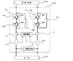
- FIG. 1 is a circuit diagram showing a configuration of a circuit breaker according to Embodiment 1 of the present invention.
- a circuit breaker 100 is connected to a DC circuit 200, and is connected in series to first switching contacts 1a and 1b that open and close the DC circuit 200, and to the first switching contacts 1a and 1b, respectively.
- the second switching contacts 2a and 2b for opening and closing the electric circuit 200, the switching mechanism 3 for opening and closing the first switching contacts 1a and 1b and the second switching contacts 2a and 2b, and both ends of the second switching contacts 2a and 2b Are connected in parallel to each other, and the semiconductor switches 4a and 4b for opening and closing the DC circuit 200, and when the current flowing through the DC circuit 200 exceeds a predetermined value, the switching mechanism 3 is driven in a time limit corresponding to the value of the current.
- Tripping devices 5a and 5b for blocking the first switching contacts 1a and 1b, and a gate drive circuit connected to the load side of the tripping device 5a and the load side of the tripping device 5b and driving the semiconductor switches 4a and 4b It is equipped with a door.
- the second switching contacts 2a and 2b are opened and closed in conjunction with the switching operation of the first switching contacts 1a and 1b.
- a semiconductor element 4a1 in which diodes 4a3 are connected in antiparallel and a semiconductor element 4a2 in which diodes 4a4 are connected in antiparallel are connected in series with opposite polarities.
- the semiconductor element 4b1 having the diode 4b3 connected in antiparallel and the semiconductor element 4b2 having the diode 4b4 connected in antiparallel are connected in series with opposite polarities.
- the semiconductor switches 4a and 4b are turned on by being driven by the gate drive circuit 6.
- the first switching contacts 1a and 1b, the second switching contacts 2a and 2b, and the semiconductor switches 4a and 4b are turned on.
- the on-resistance of the semiconductor switches 4a and 4b is larger than the on-resistance of the second switching contacts 2a and 2b, the current substantially flows through the second switching contacts 2a and 2b.
- the opening / closing mechanism 3 is driven by an operation switch (not shown) or tripping devices 5a, 5b, and first, opening operation of the first opening / closing contacts 1a, 1b is started.
- an operation switch not shown
- tripping devices 5a, 5b tripping devices
- the opening operation of the first switching contacts 1a and 1b further proceeds, the opening operation of the second switching contacts 2a and 2b is also started.
- the second switching contacts 2a and 2b are separated, an arc is generated between the contacts of the second switching contacts 2a and 2b, and the voltage between the contacts of the second switching contacts 2a and 2b increases.
- the current flowing between the first switching contacts 1a and 1b and the second switching contacts 2a and 2b is further limited, and the current flowing through the second switching contacts 2a and 2b is limited to the semiconductor switch 4a, 4b will be commutated.
- the gate drive circuit 6 The gate drive of the semiconductor switches 4a and 4b is stopped and the semiconductor switches 4a and 4b are turned off, whereby the interruption of the DC circuit 200 is completed.
- the delay operation in which the gate drive of the semiconductor switches 4a and 4b of the gate drive circuit 6 is stopped after the second switching contacts 2a and 2b are opened can be configured based on a signal from the switching mechanism 3. is there.
- an arc is generated between the contacts of the first switching contacts 1a and 1b, and an arc is generated between the contacts of the second switching contacts 2a and 2b. Since the voltage between the contacts increases and the voltage applied to the gate drive circuit 6 decreases, it is possible to configure a circuit for a delay operation based on the decrease in the voltage.
- the first switching contacts 1a and 1b are shown on the DC circuit 200 side, and the second switching contacts 2a and 2b are shown on the load 300 side.
- 1a and 1b may be provided on the load 300 side, and the second switching contacts 2a and 2b may be provided on the DC circuit 200 side.
- the gate drive circuit 6 is desirably provided on the load 300 side with respect to the first switching contacts 1a and 1b and the second switching contacts 2a and 2b.
- it is provided between the first switching contacts 1a and 1b and the second switching contacts 2a and 2b, and power is supplied to the gate drive circuit 6 by either the normal connection or the reverse connection. A configuration in which is blocked is desirable.
- the first switching contacts 1a and 1b for opening and closing the DC circuit 200 the semiconductor switches 4a and 4b connected in series with the first switching contacts 1a and 1b, and the semiconductor switch 4a. 4b, the second switching contacts 2a and 2b connected in parallel to both ends of the semiconductor switch 4a and 4b are provided.
- the semiconductor switches 4a and 4b are turned on, the first switching contacts 1a and 1b and the second switching contacts 2a and 2b are closed. Since it is closed after the formation and is opened after the first switching contacts 1a and 1b and the second switching contacts 2a and 2b are opened, the DC current from a small current to a ground fault current can be stably blocked. Can do.
- the switching mechanism 3 is configured to close the second switching contacts 2a and 2b earlier than the first switching contacts 1a and 1b and open the second switching contacts 2a and 2b later than the first switching contacts 1a and 1b. Since the cut-off current at the time of cut-off is sufficiently limited by the opening of the first switch contacts 1a and 1b, commutation from the second switch contacts 2a and 2b to the semiconductor switches 4a and 4b is performed. Therefore, there is no possibility of damaging the semiconductor switches 4a and 4b.
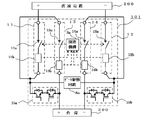
- FIG. FIG. 2 is a circuit diagram showing the configuration of the circuit breaker according to Embodiment 2 of the present invention
- FIG. 3 is a block diagram showing the schematic configuration of the circuit breaker according to Embodiment 2 of the present invention.
- the circuit breaker 101 includes a pole 11 having one end connected to the positive electrode of the DC circuit 200 and the first switching contact 11a, and one end connected to the negative electrode of the DC circuit 200.
- a pole 12 provided with a contact 12a, a pole 13 provided with one end connected to the other end of the pole 11 and a second switching contact 13a, and a second switching contact provided with the other end of the pole 12 connected to one end.
- the open / close mechanism 3a for opening and closing the first open / close contacts 11a and 12a and the second open / close contacts 13a and 14a is connected between the other end of the pole 11 and the other end of the pole 12, and the gates of the semiconductor switches 15a and 15b.
- Drive circuit for driving And a a circuit breaker 4-pole equipped with.
- a load 300 is connected to the other end of the pole 13 and the other end of the pole 14.
- a tripping device 11b is provided between the first switching contact 11a and the other end of the pole 11, and a tripping device 12b is provided between the first switching contact 12a and the other end of the pole 12, and a second switching contact 13a.
- a tripping device 13b is provided between the other end of the pole 13 and a tripping device 14b is provided between the second switching contact 14a and the other end of the pole 14, respectively. Since the configuration of the semiconductor switches 15a and 15b is the same as the configuration of the semiconductor switches 4a and 4b described in the first embodiment, the description thereof is omitted.
- the opening distance of the first switching contacts 11a and 12a is set larger than the opening distance of the second switching contacts 13a and 14a. Due to the difference in the opening distance, the second switching contacts 13a, 14a are closed earlier than the first switching contacts 11a, 12a when being turned on, and the second switching contacts 13a, 14a are closed when shutting off. It is opened later than the switching contacts 11a and 12a.
- the operation of the circuit breaker 101 will be described. First, the closing operation of the circuit breaker 101 will be described.
- the opening distance of the second switching contacts 13a, 14a is the first switching Since it is smaller than the opening distance of the contacts 11a, 12a, the closing operation of the second switching contacts 13a, 14a is completed first, and then the closing operation of the first switching contacts 11a, 12a is completed. Thereby, the current of the DC circuit 200 starts to flow through the circuit breaker 101.
- the semiconductor switches 15a and 15b are turned on by being driven by the gate drive circuit 6a. Thereby, the first switching contacts 11a and 12a, the second switching contacts 13a and 14a, and the semiconductor switches 15a and 15b are turned on. At this time, since the ON resistance of the semiconductor switches 15a and 15b is larger than the ON resistance of the second switching contacts 13a and 14a, the current substantially flows through the second switching contacts 13a and 14a.
- the opening / closing mechanism 3a is driven by an operation switch (not shown) or tripping devices 11b, 12b, 13b, 14b, and first, the opening operation of the first switching contacts 11a, 12a is started.
- an arc is generated between the first switching contacts 11a and 12a, and the current flowing between the first switching contacts 11a and 12a is limited. It is.
- the opening operation of the first switching contacts 11a and 12a further proceeds, the opening operation of the second switching contacts 13a and 14a is started, and an arc is generated between the respective contacts of the second switching contacts 13a and 14a.
- the voltage between the second switching contacts 13a and 14a increases. Due to the voltage increase between the contacts, currents flowing through the second switching contacts 13a and 14a are commutated to the semiconductor switches 15a and 15b, respectively.
- the gate drive circuit 6a Stops the gate drive of the semiconductor switches 15a and 15b, and the semiconductor switches 15a and 15b are turned off, whereby the interruption of the DC circuit 200 is completed.
- the switching contacts 11a and 12a provided on the poles 11 and 12 to which the DC circuit 200 is connected at one end are used as the first switching contact in the claims, and the load 300 is connected to the other end.
- the open / close contacts 13a and 14a provided on the poles 13 and 14 are the second open / close contacts in the claims, but the open / close contacts 11a and 12a are the second open / close contacts and the open / close contacts 13a and 14a are the second open / close contacts.
- One switching contact may be used. In that case, the opening distance of the switching contacts 11a, 12a is set smaller than the opening distance of the switching contacts 13a, 14a.
- the first switching contacts 11a and 12a that open and close the DC circuit 200, the semiconductor switches 15a and 14b connected in series with the first switching contacts 11a and 12a, the semiconductor switch 15a, The second switch contacts 13a and 14a connected in parallel to both ends of the switch 14b are provided.
- the semiconductor switches 15a and 14b are turned on, the first switch contacts 11a and 12a and the second switch contacts 13a and 14a are closed. It is closed later, and at the time of interruption, it is opened after the opening of the first switching contacts 11a, 12a and the second switching contacts 13a, 14a, so that it is possible to stably cut off a direct current from a small current to a ground fault current. it can.
- an opening / closing mechanism 3a for closing the second switching contacts 13a, 14a earlier than the first switching contacts 11a, 12a and opening the second switching contacts 13a, 14a later than the first switching contacts 11a, 12a is provided. Since the cut-off current at the time of cut-off is sufficiently limited by the opening of the first switch contacts 11a and 12a, commutation from the second switch contacts 13a and 14a to the semiconductor switches 15a and 15b is performed. Therefore, there is no possibility of damaging the semiconductor switches 15a and 15b.
- the second switching contacts 13a, 14a By making the opening distance of the first switching contacts 11a, 12a larger than the opening distance of the second switching contacts 13a, 14a, the second switching contacts 13a, 14a earlier than the first switching contacts 11a, 12a. Is closed and the second switching contacts 13a and 14a are opened later than the first switching contacts 11a and 12a, so that the existing switching mechanism 3a can be used.
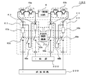
- FIG. 4 is a circuit diagram showing the configuration of the circuit breaker according to the second embodiment of the present invention
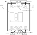
- FIG. 5 is a front view showing the circuit breaker according to the third embodiment of the present invention
- FIG. 6 is a line x ⁇ shown in FIG.
- FIG. 7 is a cross-sectional view taken along line yy shown in FIG. 4, and
- FIG. 8 is an operation of the first switch contact, the second switch contact, the crossbar, and the actuator shown in FIG. (A) is an OFF state, (b) is a state during the operation from OFF to ON, and (c) is an ON state.
- the circuit breaker 102 has a pole 41 having one end connected to the positive electrode of the DC circuit 200 and a first switching contact 41a, and one end connected to the negative electrode of the DC circuit 200 and a first switching contact 42a.
- a pole 43 having one end connected to the positive electrode of the load 300 and the first switching contact 43a, and a terminal having one end connected to the negative electrode of the load 300 and the first switching contact 44a.
- a tripping device 41b is provided between the first switching contact 41a and the other end of the pole 41, and a tripping device 42b is provided between the first switching contact 42a and the other end of the pole 42, and the first switching contact 43a.
- a tripping device 43 b is provided between the other end of the pole 43 and a tripping device 44 b is provided between the first switching contact 44 a and the other end of the pole 44.
- a second switching contact 46 a is connected in parallel to the semiconductor switch 45 a between the other end of the pole 41 and the other end of the pole 43, and between the other end of the pole 42 and the other end of the pole 44.
- the second switching contact 46b is connected in parallel to the semiconductor switch 45b.
- the configuration of the semiconductor switches 45a and 45b is the same as the configuration of the semiconductor switches 4a and 4b described in the first embodiment, and a description thereof will be omitted.
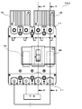
- the circuit breaker 102 is configured by using a housing 20 including a base 20 a and a cover 20 b made of an insulating material.
- the poles 41 to 44 are arranged in parallel with each other on the base 20a, and an opening / closing mechanism 30 having a well-known toggle link mechanism is arranged on the top of the poles 41 to 44.
- the cover 20b covers each pole on the base 20a and the opening / closing mechanism 30, and the operation handle 31 of the opening / closing mechanism 30 projects from the window 20b1 of the cover 20b.
- the poles are configured in the same manner, and the cross bar 32 is disposed on the base 20a so as to be orthogonal to the poles 41 to 44.
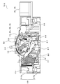
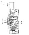
- Each pole has a power supply side terminal 24 provided on the base 20 a, a fixed contact 21 provided on a fixed contact 27 extending from the power supply side terminal 24, and a movable contacted with and separating from the fixed contact 21.
- the fixed contact 21 and the movable contact 22 of each pole constitute first switching contacts 41a, 42a, 43a, 44a that first open and close the electric circuit when a large current is interrupted.
- the opening / closing mechanism 30 includes a known toggle link mechanism, and includes a known trip bar 33 driven by tripping devices 41b, 42b, 43b, and 44b.
- the circuit breaker 102 is provided on both sides of the opening / closing mechanism 30, and is provided on both sides of the opening / closing mechanism 30, as well as the actuators 28 a and 28 b respectively driven by the rotation of the crossbar 32.
- second open / close contacts 46a and 46b that are driven by actuators 28a and 28b to open and close the contacts.
- the second switching contacts 46a and 46b are the contacts of the switching contacts of the second switching contacts 46a and 46b when the button 461 is pressed by the actuators 28a and 28b.
- the movable contacts 22 constituting the first switching contacts 41a, 42a, 43a, 44a come into contact with the fixed contacts 21, respectively, as shown in FIG.
- the voltage of the DC circuit 200 is applied to the gate drive circuit 6, and the semiconductor switches 45a and 45b are turned on after a predetermined delay time.
- the contact resistance of the second switching contacts 46a and 46b is smaller than the ON resistance of the semiconductor switches 45a and 45b, so that the current is mainly the second switching contact. Since it flows through 46a and 46b, the heat generation of the semiconductor switches 45a and 45b is suppressed.
- the purpose of the first switching contact may be a voltage that cannot be interrupted only by the arc-extinguishing device 50, which is a current limiting current for interrupting a large current.
- the first switching contact is opened at the same time as the crossbar 32 starts to rotate, and the arc extinguishing device 50 is configured so that the current is kept below the rated current of the semiconductor switches 45a and 45b immediately before the maximum opening.
- the second switching contacts 46a and 46b are opened immediately before the crossbar 32 is fully opened, and the current limited thereby is commutated to the semiconductor switches 45a and 45b.
- the current is also limited between the first switching contacts 41a, 42a, 43a, 44a, and the voltage drop is large, whereby the supply voltage to the gate drive circuit 6 that drives the semiconductor switches 45a, 45b. Decreases.
- the gate voltage of the semiconductor switches 45a and 45b is secured by a time delay circuit of the gate drive circuit 6 for a predetermined time (for example, 15 msec). Then, after a predetermined time has passed, the gates of the semiconductor switches 45a and 45b are turned off when the energization current becomes equal to or lower than the rated current, and the cutoff operation is completed.
- the first switching contacts 41a, 42a, 43a, 44a that open and close the DC circuit 200, and the semiconductor switch 45a connected in series with the first switching contacts 41a, 42a, 43a, 44a. , 45b and second switching contacts 46a, 46b connected in parallel to both ends of the semiconductor switches 45a, 45b.
- the semiconductor switches 45a, 45b are turned on, the first switching contacts 41a, 42a, 43a, 44a are provided.
- the second switching contacts 46a, 46b are closed, and at the time of interruption, the first switching contacts 41a, 42a, 43a, 44a and the second switching contacts 46a, 46b are opened.
- DC current from the ground fault current to the ground fault current can be stably interrupted.
- each fixed contact 21 and each movable contact 22 that contacts and separates from this fixed contact 21 are provided for four poles, that is, four sets, so that a higher voltage than in the case of two sets is provided.
- the DC circuit can be shut off.
Landscapes
- Engineering & Computer Science (AREA)
- Power Engineering (AREA)
- Driving Mechanisms And Operating Circuits Of Arc-Extinguishing High-Tension Switches (AREA)
- Breakers (AREA)
- Keying Circuit Devices (AREA)
Abstract
Description
そのため、開閉接点の開離距離を大きくすることなく、直流回路を遮断する方式として、開閉接点間に半導体スイッチを並列接続し、開閉接点の開閉動作時に電流を半導体スイッチに転流させて開閉接点間に生じたアークを素早く消滅させた後、この半導体スイッチをOFFして電流を遮断する技術が提案されている(例えば、特許文献1および2参照)。
図1において、回路遮断器100は、直流電路200に接続され、直流電路200を開閉する第一の開閉接点1a、1bと、この第一の開閉接点1a、1bにそれぞれ直列に接続され、直流電路200を開閉する第二の開閉接点2a、2bと、第一の開閉接点1a、1bおよび第二の開閉接点2a、2bを開閉する開閉機構3と、第二の開閉接点2a、2bの両端にそれぞれ並列に接続され、直流電路200を開閉する半導体スイッチ4a、4bと、直流電路200を流れる電流が所定の値を超えると、その電流の値に応じた時限で開閉機構3を駆動して第一の開閉接点1a、1bを遮断する引外し装置5a、5bと、引外し装置5aの負荷側および引外し装置5bの負荷側に接続され、半導体スイッチ4a、4bを駆動するゲート駆動回路6とを備えている。
また、第二の開閉接点2a、2bは、第一の開閉接点1a、1bの開閉動作に連動し、開閉される。
また、半導体スイッチ4bは、ダイオード4b3を逆並列に接続した半導体素子4b1と、ダイオード4b4を逆並列に接続した半導体素子4b2とが互いに逆極性に直列接続されている。
開閉機構3を操作し、第一の開閉接点1a、1bおよび第二の開閉接点2a、2bの閉成動作を行うと、まず、第二の開閉接点2a、2bの閉成動作が完了し、その後に第一の開閉接点1a、1bの閉成動作が完了する。これにより、回路遮断器100を直流電路200の電流が流れ始める。
図示しない操作スイッチ、もしくは、引外し装置5a、5bに開閉機構3が駆動され、まず、第一の開閉接点1a、1bの開離動作が開始される。第一の開閉接点1a、1bが開離すると、第一の開閉接点1a、1bの各接点間にアークが発生し、第一の開閉接点1a、1bの各接点間を流れる電流は限流される。
図2は本発明の実施の形態2における回路遮断器の構成を示す回路図、図3は本発明の実施の形態2における回路遮断器の概略構成を示す構成図である。
図2、3において、回路遮断器101は、一端に直流電路200の正極が接続され第一の開閉接点11aが設けられた極11と、一端に直流電路200の負極が接続され第一の開閉接点12aが設けられた極12と、、一端に極11の他端が接続され第二の開閉接点13aが設けられた極13と、一端に極12の他端が接続され第二の開閉接点14aが設けられた極14と、極11の他端および極13の他端間に接続された半導体スイッチ15aと、極12の他端および極14の他端間に接続された半導体スイッチ15bと、第一の開閉接点11a、12a、および第二の開閉接点13a、14aを開閉する開閉機構3aと、極11の他端および極12の他端間に接続され、半導体スイッチ15a、15bのゲートを駆動するゲート駆動回路6aと、を備えた4極の回路遮断器である。そして、極13の他端および極14の他端には負荷300が接続されている
次に、回路遮断器101の動作について説明する。まず、回路遮断器101の投入動作について説明する。
図示しない操作スイッチもしくは、引外し装置11b、12b、13b、14bによって、開閉機構3aが駆動され、まず、第一の開閉接点11a、12aの開離動作が開始される。第一の開閉接点11a、12aが開離されると、第一の開閉接点11a、12aの各接点間にアークが発生し、第一の開閉接点11a、12aの各接点間を流れる電流は限流される。
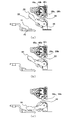
図4は本発明の実施の形態2における回路遮断器の構成を示す回路図、図5は本発明の実施の形態3における回路遮断器を示す正面図、図6は図4に示す線x-xに沿った断面図、図7は図4に示す線y-yに沿った断面図、図8は図7に示す第一の開閉接点、第二の開閉接点、クロスバー、およびアクチュエータの動作を説明するための説明図で、(a)はOFF状態、(b)はOFFからONへの動作途中の状態、(c)はON状態である。
さらに、極41の他端と極43の他端の間には、第二の開閉接点46aが半導体スイッチ45aに対し並列接続されており、極42の他端と極44の他端の間には、第二の開閉接点46bが半導体スイッチ45bに対し並列接続されている。半導体スイッチ45a、45bの構成は、実施の形態1で説明した半導体スイッチ4a、4bの構成と同様なので説明は省略する。
各極は、互いに同じに構成され、クロスバー32は、各極41~44に直交するように、ベース20a上に配置されている。
各極の固定接点21と可動接点22とで、大電流遮断時に電路を最初に開閉する第一の開閉接点41a、42a、43a、44aをそれぞれ構成している。
また、開閉機構30は、周知のトグルリンク機構からなり、引外し装置41b、42b、43b、44bにより駆動される周知のトリップバー33を備えている。
第二の開閉接点46a、46bは、アクチュエータ28a、28bによりボタン461を押下されると、第二の開閉接点46a、46bの開閉接点が接触するものである。
まず、投入動作について説明する。
図8に示すように、操作ハンドル31を投入すると開閉機構30のトグルリンクがデッドポイントを超えることで、クロスバー32が、図8(a)の状態から図8(b)の状態ので図8の紙面上、反時計方向に回動を始める。このクロスバー32の回動により、アクチュエータ28a、28bも図8の紙面上、反時計方向に回動し、図8(b)に示すように、アクチュエータ28a、28bによりボタン461が押下される。このボタン461の押下により第二の開閉接点46a、46bが接触状態となる。
短絡電流や過電流が流れると引外し装置41b、42b、43b、44bが、トリップバー33を押し開閉機構30が駆動されることにより、クロスバー32が回動を開始する。クロスバー32の回動により、可動接点22が固定接点21から開離する。これにより、第一の開閉接点41a、42a、43a、44aがまず開離する。可動接点22が開離した際、この開離距離に対して十分な直流高電圧であることから、アーク電流は固定接点21と可動接点間22の最短距離で維持しようとする。今回、第一の開閉接点の目的は、消弧装置50のみでは遮断できない電圧であることもあり、大電流遮断時の遮断電流の限流となる。その第一の開閉接点はクロスバー32が回動始めると同時に開離し最大開離直前までに電流を半導体スイッチ45a、45bの定格電流以下に抑えるように消弧装置50が構成されている。
2a 第二の開閉接点、2b 第二の開閉接点、3 開閉機構、
4a 半導体スイッ、4b 半導体スイッチ、5a 引外し装置、5b 引外し装置、
100 回路遮断器。
Claims (6)
- 電路を開閉する第一の開閉接点と、この第一の開閉接点に直列に接続され、前記電路を開閉する第二の開閉接点と、前記第二の開閉接点の両端に並列に接続され、前記電路を開閉する半導体スイッチと、を備え、
前記半導体スイッチは、投入時には前記第一の開閉接点および前記第二の開閉接点の閉成後に閉成され、遮断時には前記第一の開閉接点および前記第二の開閉接点の開成後に開成されることを特徴とする回路遮断器。 - 前記第一の開閉接点より早く前記第二の開閉接点を閉成し、前記第一の開閉接点より遅く前記第二の開閉接点を開成する開閉機構を備えたことを特徴とする請求項1に記載の回路遮断器。
- 4極の回路遮断器において、前記第一の開閉接点は一端に前記電路もしくは負荷のいずれかが接続された2極に設けられており、前記第二の開閉接点は一端に前記2極の他端および前記半導体スイッチの一端がそれぞれ接続され、他端に前記半導体スイッチの他端がそれぞれ接続された他の2極に設けられていることを特徴とする請求項1または請求項2に記載の回路遮断器。
- 前記第一の開閉接点の開離距離は、前記第二の開閉接点の開離距離より大きいことを特徴とする請求項3に記載の回路遮断器。
- 4極の回路遮断器において、前記第一の開閉接点は、一端に前記電路の正極および負極がそれぞれ接続された2極と、一端に負荷の正極および負極がそれぞれ接続された他の2極とに設けられており、
前記半導体スイッチは、前記2極の他端間、および前記他の2極の他端間にそれぞれ接続されており、
前記第二の開閉接点は、前記開閉機構の極の配列方向における前記開閉機構の両側にそれぞれ設けられ、前記半導体スイッチの両端間にそれぞれ並列接続されていることを特徴とする請求項2に記載の回路遮断器。 - 前記開閉機構に駆動され、前記第二の開閉接点を開閉するアクチュエータを備えたことを特徴とする請求項5に記載の回路遮断器。
Priority Applications (5)
| Application Number | Priority Date | Filing Date | Title |
|---|---|---|---|
| JP2017540387A JP6369637B2 (ja) | 2015-09-16 | 2015-09-16 | 回路遮断器 |
| EP15904074.0A EP3352193B1 (en) | 2015-09-16 | 2015-09-16 | Circuit breaker |
| KR1020177035780A KR102010167B1 (ko) | 2015-09-16 | 2015-09-16 | 회로 차단기 |
| CN201580080942.8A CN107710369B (zh) | 2015-09-16 | 2015-09-16 | 电路断路器 |
| PCT/JP2015/076243 WO2017046885A1 (ja) | 2015-09-16 | 2015-09-16 | 回路遮断器 |
Applications Claiming Priority (1)
| Application Number | Priority Date | Filing Date | Title |
|---|---|---|---|
| PCT/JP2015/076243 WO2017046885A1 (ja) | 2015-09-16 | 2015-09-16 | 回路遮断器 |
Publications (1)
| Publication Number | Publication Date |
|---|---|
| WO2017046885A1 true WO2017046885A1 (ja) | 2017-03-23 |
Family
ID=58288286
Family Applications (1)
| Application Number | Title | Priority Date | Filing Date |
|---|---|---|---|
| PCT/JP2015/076243 Ceased WO2017046885A1 (ja) | 2015-09-16 | 2015-09-16 | 回路遮断器 |
Country Status (5)
| Country | Link |
|---|---|
| EP (1) | EP3352193B1 (ja) |
| JP (1) | JP6369637B2 (ja) |
| KR (1) | KR102010167B1 (ja) |
| CN (1) | CN107710369B (ja) |
| WO (1) | WO2017046885A1 (ja) |
Cited By (1)
| Publication number | Priority date | Publication date | Assignee | Title |
|---|---|---|---|---|
| JP2023099913A (ja) * | 2022-01-04 | 2023-07-14 | 株式会社東芝 | 直流電流遮断装置 |
Families Citing this family (1)
| Publication number | Priority date | Publication date | Assignee | Title |
|---|---|---|---|---|
| FR3116391B1 (fr) * | 2020-11-18 | 2022-12-16 | Hager Electro Sas | Appareillage de protection à coupure électronique |
Citations (6)
| Publication number | Priority date | Publication date | Assignee | Title |
|---|---|---|---|---|
| JPS627738U (ja) * | 1985-06-29 | 1987-01-17 | ||
| JPH08106839A (ja) * | 1994-10-05 | 1996-04-23 | Alps Electric Co Ltd | 機械式スイッチの接点間アークの消去装置 |
| JPH10334785A (ja) * | 1997-05-30 | 1998-12-18 | Mitsubishi Electric Corp | 気中直流遮断器、気中交流遮断器、及び気中直流遮断器の結線方法 |
| JP2002093294A (ja) * | 2000-09-18 | 2002-03-29 | Toshiba Corp | 真空直流遮断器 |
| JP2012248445A (ja) * | 2011-05-30 | 2012-12-13 | Fuji Electric Co Ltd | 開閉器 |
| JP2014241187A (ja) * | 2013-06-11 | 2014-12-25 | 富士電機株式会社 | 直流開閉器 |
Family Cites Families (6)
| Publication number | Priority date | Publication date | Assignee | Title |
|---|---|---|---|---|
| CN102165555B (zh) * | 2008-09-25 | 2014-01-15 | 松下电器产业株式会社 | 混合继电器和控制终端装置 |
| DE102011118713A1 (de) * | 2011-03-22 | 2012-09-27 | Dehn + Söhne Gmbh + Co. Kg | Ein- oder mehrpolige Schalteinrichtung, insbesondere für Gleichstromanwendungen |
| JP2014038775A (ja) | 2012-08-17 | 2014-02-27 | Fuji Electric Co Ltd | 直流回路用の回路遮断スイッチ |
| DE102012217280A1 (de) * | 2012-09-25 | 2014-03-27 | Siemens Aktiengesellschaft | Trennanordnung für ein Hochspannungsgleichstromnetz |
| KR101521545B1 (ko) * | 2013-10-07 | 2015-05-19 | 한국전기연구원 | 고압 직류 전류 차단 장치 및 방법 |
| DE102013114259A1 (de) * | 2013-12-17 | 2015-06-18 | Eaton Electrical Ip Gmbh & Co. Kg | Schaltvorrichtung zum Führen und Trennen von elektrischen Strömen |
-
2015
- 2015-09-16 EP EP15904074.0A patent/EP3352193B1/en active Active
- 2015-09-16 JP JP2017540387A patent/JP6369637B2/ja active Active
- 2015-09-16 KR KR1020177035780A patent/KR102010167B1/ko active Active
- 2015-09-16 CN CN201580080942.8A patent/CN107710369B/zh active Active
- 2015-09-16 WO PCT/JP2015/076243 patent/WO2017046885A1/ja not_active Ceased
Patent Citations (6)
| Publication number | Priority date | Publication date | Assignee | Title |
|---|---|---|---|---|
| JPS627738U (ja) * | 1985-06-29 | 1987-01-17 | ||
| JPH08106839A (ja) * | 1994-10-05 | 1996-04-23 | Alps Electric Co Ltd | 機械式スイッチの接点間アークの消去装置 |
| JPH10334785A (ja) * | 1997-05-30 | 1998-12-18 | Mitsubishi Electric Corp | 気中直流遮断器、気中交流遮断器、及び気中直流遮断器の結線方法 |
| JP2002093294A (ja) * | 2000-09-18 | 2002-03-29 | Toshiba Corp | 真空直流遮断器 |
| JP2012248445A (ja) * | 2011-05-30 | 2012-12-13 | Fuji Electric Co Ltd | 開閉器 |
| JP2014241187A (ja) * | 2013-06-11 | 2014-12-25 | 富士電機株式会社 | 直流開閉器 |
Cited By (2)
| Publication number | Priority date | Publication date | Assignee | Title |
|---|---|---|---|---|
| JP2023099913A (ja) * | 2022-01-04 | 2023-07-14 | 株式会社東芝 | 直流電流遮断装置 |
| JP7638916B2 (ja) | 2022-01-04 | 2025-03-04 | 株式会社東芝 | 直流電流遮断装置 |
Also Published As
| Publication number | Publication date |
|---|---|
| CN107710369A (zh) | 2018-02-16 |
| EP3352193A1 (en) | 2018-07-25 |
| EP3352193B1 (en) | 2019-12-11 |
| EP3352193A4 (en) | 2018-09-26 |
| CN107710369B (zh) | 2019-06-18 |
| KR102010167B1 (ko) | 2019-08-12 |
| KR20180004812A (ko) | 2018-01-12 |
| JPWO2017046885A1 (ja) | 2017-12-07 |
| JP6369637B2 (ja) | 2018-08-08 |
Similar Documents
| Publication | Publication Date | Title |
|---|---|---|
| JP5522327B2 (ja) | 回路遮断器 | |
| CN103247499B (zh) | 混合电流开关装置 | |
| CN104321847B (zh) | 直流电路用电路断路器以及直流电路用电路断路装置 | |
| CN104143809B (zh) | 直流电流切换设备、电子装置和切换关联直流电路的方法 | |
| RU2581599C2 (ru) | Выключатель с дугогасительной камерой | |
| US11626263B2 (en) | Dual-action switching mechanism and pole unit for circuit breaker | |
| US8686311B2 (en) | Breaking device with arc breaking shield | |
| CN106663557A (zh) | 用于中断直流电流的分离开关 | |
| JP2012248445A (ja) | 開閉器 | |
| KR20150141866A (ko) | 회로 차단기 | |
| WO2020087797A1 (zh) | 无极性低压断路器 | |
| CN118511242A (zh) | 使气隙致动器和固态开关部件同时跳闸或者使固态开关部件延迟跳闸的固态断路器 | |
| US9312081B2 (en) | Arcless fusible switch disconnect device for DC circuits | |
| US10269512B2 (en) | Method and device for cutting off an electric current with dynamic magnetic blow-out | |
| JP6369637B2 (ja) | 回路遮断器 | |
| JP6302663B2 (ja) | 直流開閉器 | |
| JP2012089295A (ja) | 回路遮断器 | |
| JP3587983B2 (ja) | 電力開閉装置 | |
| KR100885849B1 (ko) | 컨택트 온 기구를 가지는 배선용 차단기 | |
| KR102056237B1 (ko) | 배선용차단기 | |
| JPS5934043Y2 (ja) | 回路しや断器 | |
| JP2023074076A (ja) | 回路遮断器 | |
| KR200326453Y1 (ko) | 차단기의 접촉자 구조 | |
| JPH0458432A (ja) | 回路遮断器 | |
| JPH0896668A (ja) | ガス遮断器 |
Legal Events
| Date | Code | Title | Description |
|---|---|---|---|
| 121 | Ep: the epo has been informed by wipo that ep was designated in this application |
Ref document number: 15904074 Country of ref document: EP Kind code of ref document: A1 |
|
| ENP | Entry into the national phase |
Ref document number: 2017540387 Country of ref document: JP Kind code of ref document: A |
|
| ENP | Entry into the national phase |
Ref document number: 20177035780 Country of ref document: KR Kind code of ref document: A |
|
| NENP | Non-entry into the national phase |
Ref country code: DE |
|
| WWE | Wipo information: entry into national phase |
Ref document number: 2015904074 Country of ref document: EP |