WO2017047381A1 - 導波管スロットアンテナおよびその製造方法 - Google Patents
導波管スロットアンテナおよびその製造方法 Download PDFInfo
- Publication number
- WO2017047381A1 WO2017047381A1 PCT/JP2016/075405 JP2016075405W WO2017047381A1 WO 2017047381 A1 WO2017047381 A1 WO 2017047381A1 JP 2016075405 W JP2016075405 W JP 2016075405W WO 2017047381 A1 WO2017047381 A1 WO 2017047381A1
- Authority
- WO
- WIPO (PCT)
- Prior art keywords
- waveguide
- slot antenna
- forming member
- radiation
- axis direction
- Prior art date
- Legal status (The legal status is an assumption and is not a legal conclusion. Google has not performed a legal analysis and makes no representation as to the accuracy of the status listed.)
- Ceased
Links
Images








Classifications
-
- H—ELECTRICITY
- H01—ELECTRIC ELEMENTS
- H01Q—ANTENNAS, i.e. RADIO AERIALS
- H01Q13/00—Waveguide horns or mouths; Slot antennas; Leaky-waveguide antennas; Equivalent structures causing radiation along the transmission path of a guided wave
- H01Q13/10—Resonant slot antennas
- H01Q13/18—Resonant slot antennas the slot being backed by, or formed in boundary wall of, a resonant cavity ; Open cavity antennas
-
- H—ELECTRICITY
- H01—ELECTRIC ELEMENTS
- H01P—WAVEGUIDES; RESONATORS, LINES, OR OTHER DEVICES OF THE WAVEGUIDE TYPE
- H01P11/00—Apparatus or processes specially adapted for manufacturing waveguides or resonators, lines, or other devices of the waveguide type
- H01P11/001—Manufacturing waveguides or transmission lines of the waveguide type
- H01P11/002—Manufacturing hollow waveguides
-
- H—ELECTRICITY
- H01—ELECTRIC ELEMENTS
- H01P—WAVEGUIDES; RESONATORS, LINES, OR OTHER DEVICES OF THE WAVEGUIDE TYPE
- H01P3/00—Waveguides; Transmission lines of the waveguide type
- H01P3/12—Hollow waveguides
-
- H—ELECTRICITY
- H01—ELECTRIC ELEMENTS
- H01Q—ANTENNAS, i.e. RADIO AERIALS
- H01Q21/00—Antenna arrays or systems
- H01Q21/0006—Particular feeding systems
- H01Q21/0037—Particular feeding systems linear waveguide fed arrays
- H01Q21/0043—Slotted waveguides
- H01Q21/005—Slotted waveguides arrays
-
- H—ELECTRICITY
- H01—ELECTRIC ELEMENTS
- H01Q—ANTENNAS, i.e. RADIO AERIALS
- H01Q21/00—Antenna arrays or systems
- H01Q21/0006—Particular feeding systems
- H01Q21/0037—Particular feeding systems linear waveguide fed arrays
- H01Q21/0043—Slotted waveguides
- H01Q21/0062—Slotted waveguides the slots being disposed around the feeding waveguide
-
- H—ELECTRICITY
- H01—ELECTRIC ELEMENTS
- H01Q—ANTENNAS, i.e. RADIO AERIALS
- H01Q21/00—Antenna arrays or systems
- H01Q21/06—Arrays of individually energised antenna units similarly polarised and spaced apart
- H01Q21/061—Two dimensional planar arrays
- H01Q21/064—Two dimensional planar arrays using horn or slot aerials
Definitions
- the present invention relates to a waveguide slot antenna and a manufacturing method thereof.
- a waveguide slot antenna is used in various electric and electronic devices (systems) having a wireless communication function, such as a radio wave in a high frequency band (for example, a radio wave in a millimeter wave band) or a radio wave in a low frequency band (for example, It is used as an antenna for transmitting and receiving centimeter wave radio waves).
- Millimeter-wave radio waves are used in, for example, in-vehicle radar systems, and centimeter-wave radio waves are used in satellite broadcasting systems such as broadcasting satellites (BS) and communication satellites (CS), wireless LANs, and Bluetooth (registered trademark). ) And the like, and an electronic fee collection system abbreviated as ETC (registered trademark).
- the millimeter wave band radio wave is a radio wave having a wavelength of 1 to 10 mm and a frequency of 30 to 300 GHz
- the centimeter wave band radio wave is a radio wave having a wavelength of 10 to 100 mm and a frequency of 3 to 30 GHz.
- Patent Document 1 a resin-made waveguide having a waveguide extending in the tube axis direction, in which the defined surface of the waveguide is coated with a conductive coating, and the waveguide in the tube axis direction. And a plurality of radiating slots provided at predetermined intervals along the waveguide, and the waveguide has an end shape in cross section (cross section orthogonal to the tube axis direction), and is coupled to the other side of the waveguide.
- a waveguide slot antenna composed of first and second waveguide forming members that define
- an object of the present invention is to realize a waveguide slot antenna that can stably exhibit desired antenna characteristics.
- the first invention of the present application which was created to achieve the above object, is a resin-made waveguide having a waveguide extending in the tube axis direction and having a defined surface of the waveguide covered with a conductive coating. And a plurality of radiation slots provided at predetermined intervals along the tube axis direction of the waveguide, wherein the waveguide has a cross-section at each part in the extending direction of the waveguide.
- both the first and second waveguide forming members hold the core metal (core metal extending in the tube axis direction) arranged along the tube axis direction
- both waveguides are provided. Since the bending rigidity and torsional rigidity of the waveguide composed of the combined tube-forming members can be increased, the deformation of the waveguide (particularly warping / bending in the direction along the tube axis direction) hardly occurs due to temperature changes. Become. For this reason, the waveguide slot antenna which can reduce the possibility that the above-mentioned malfunctions occur as much as possible and can stably exhibit desired antenna characteristics can be realized.
- At least one of the first and second waveguide forming members can be a resin injection-molded product having a core metal integrally (resin injection-molded product using the core metal as an insert part).
- core metal integrally
- the core metal is composed of a combination of the first core metal and the second core metal
- the first waveguide forming member is a resin injection-molded product integrally including the first core metal (first And a second waveguide forming member as a resin injection-molded product (second core metal) integrally including the second core metal. It is also possible to use a resin injection-molded product having an insert part. In this way, both the first and second waveguide forming members can be prevented from being deformed due to molding shrinkage as much as possible, so that the waveguide slot antenna having further excellent antenna characteristics. Can be obtained stably.
- the cored bar may be embedded in the wall portion of the waveguide, or a part thereof may be exposed on the outer surface of the waveguide.
- Both the first and second waveguide forming members may have a concave cross section.
- the second invention of the present application which was created to achieve the above object, is provided with a waveguide having a waveguide extending in the tube axis direction and at a predetermined interval along the tube axis direction of the waveguide.
- a plurality of radiation slots, and a waveguide is formed of a combination of first and second waveguide forming members each having an end-shaped cross section at each portion in the extending direction of the waveguide.
- the first waveguide forming member is formed of a flat metal member having a plurality of radiation slots
- the second waveguide forming member is formed of the first waveguide. It is composed of a resin member that integrally holds the member, and at least a defined surface of the waveguide of the waveguide is covered with a continuous conductive film.
- the waveguide slot antenna having the above configuration inserts a first waveguide forming member made of a flat metal member having a plurality of radiation slots, and injection-molds the second waveguide forming member with a resin.
- a waveguide can be obtained, and thereafter, this waveguide can be manufactured by performing a process of forming a conductive film covering at least the defined surface of the waveguide.
- the first waveguide forming member made of a flat metal member is inserted, and the second waveguide forming member is injection-molded with resin to obtain a waveguide.
- the first waveguide forming member can function as a reinforcing member, deformation of the second waveguide forming member (particularly warping / bending in the direction of the tube axis) due to molding shrinkage is made as much as possible. While preventing, it is possible to obtain a waveguide that is less likely to be deformed due to a temperature change or the like at a low cost.
- the second waveguide forming member integrally holds the first waveguide forming member, and at least one of the waveguides composed of a combination of the two waveguide forming members.
- the radio wave propagating through the waveguide leaks to the outside at the coupling portion of both waveguide forming members. It is possible to effectively prevent formation of a gap. From the above, a waveguide slot antenna that can stably exhibit desired antenna characteristics can be realized at low cost.
- the first waveguide forming member further includes a hole provided on the front side in the radiation direction of the radio wave radiated to the outside through the radiation slot, and the radiation slot is disposed on the inner periphery. Can be. By providing such a hole, unnecessary radiation, also called a grating lobe, can be eliminated, so that the antenna characteristics of the waveguide slot antenna can be improved.
- the first waveguide forming member can be composed of a laminate of a first metal plate having a radiation slot and a second metal plate having the hole. If it does in this way, let each of the 1st metal plate which has a radiation slot, and the 2nd metal plate which has the above-mentioned hole be a press-molded article obtained by giving press processing (punching processing) to a metal plate. Therefore, the first waveguide forming member having the radiation slot and the hole can be manufactured at a low cost.
- the conductive coating can also be formed continuously along the outer surface of the waveguide.
- a conductive film (waveguide) can be obtained by subjecting the waveguide to a conductive film formation process without performing a masking process. In this way, the masking forming process for the waveguide can be omitted, which is advantageous in reducing the cost of the waveguide slot antenna.
- a waveguide slot antenna that can stably exhibit desired antenna characteristics can be realized.
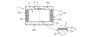
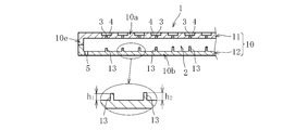
- FIG. 1 is a schematic cross-sectional view of a waveguide slot antenna according to a first embodiment of the first invention of the present application.
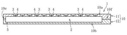
- 1B is a schematic cross-sectional view taken along line YY shown in FIG. 1A.
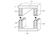
- FIG. 3 is a schematic perspective view showing an example of a method for assembling the waveguide slot antenna shown in FIG. 2. It is a schematic perspective view which shows the other example of the assembly method of a waveguide slot antenna. It is a schematic perspective view which shows the other example of the assembly method of a waveguide slot antenna.
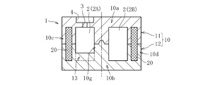
- FIG. 5B is a schematic sectional view taken along line XX in FIG. 5A.
- FIG. 5B is a schematic sectional view taken along line YY in FIG. 5A.
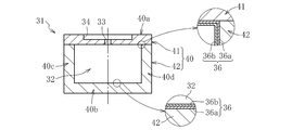
- FIG. 7A It is a schematic cross-sectional view of the waveguide slot antenna which concerns on 5th Embodiment of 1st invention of this application. It is a partial schematic plan view of the waveguide slot antenna which concerns on 1st Embodiment of 2nd invention of this application. It is the X1-X1 sectional view taken on the line of FIG. 7A. It is the Y1-Y1 sectional view taken on the line of FIG. 7A.
- FIG. 8 is a partially enlarged cross-sectional view of the waveguide slot antenna shown in FIG. 7. It is a partial expanded sectional view of the waveguide slot antenna which concerns on a modification. It is a cross-sectional view of the waveguide slot antenna which concerns on 2nd Embodiment of 2nd invention of this application.
- FIG. 10B is a sectional view taken along line X2-X2 of FIG. 10A.
- FIG. 10B is a sectional view taken along line Y2-Y2 of FIG. 10A.
- FIG. 9 is a modification of FIG. 7, and is a cross-sectional view of a waveguide slot antenna according to a fourth embodiment of the second invention of the present application.
- FIG. 1A and 1B show a schematic plan view and a schematic rear view of an antenna unit A provided with a waveguide slot antenna 1, respectively.
- This antenna unit A is for transmitting and receiving radio waves in the centimeter wave band, and includes a plurality of (in the illustrated example, five) waveguide slot antennas 1 connected in parallel and each waveguide slot.
- a feeding waveguide 9 (indicated by a two-dot chain line in FIG. 1B) for supplying high-frequency power (radio waves) to the antenna 1 is provided.
- the means for connecting the waveguide slot antennas 1 in parallel For example, fixing means such as adhesion, double-sided tape fastening, and concave-convex fitting can be used alone or in combination of two or more.
- each waveguide slot antenna 1 is, for example, a dimension in the tube axis direction (up and down direction in the drawing of FIG. 1A): 100 mm, The dimension in the width direction (left and right direction in FIG. 1A) is 20 mm, and the dimension in the height direction (direction perpendicular to the sheet in FIG. 1A) is 5 mm.
- the waveguide slot antenna 1 includes a waveguide 10 having a waveguide 2 extending in the tube axis direction therein, and a predetermined length along the tube axis direction of the waveguide 10.
- a plurality of radiation slots 3 provided at intervals, and a feeding slot 5 provided at one end in the tube axis direction of the waveguide 10 and supplying high-frequency power to the waveguide 2 are provided.
- the radiating slot 3 of the present embodiment is provided such that a straight line extending through the central portion in the width direction is inclined by 45 ° with respect to the tube axis direction.
- the inclination angle of 3 can be set as appropriate according to the application.
- the waveguide 10 is a rectangular waveguide having a rectangular cross section at each portion in the extending direction of the waveguide 2. More specifically, it includes a top wall 10a and a bottom wall 10b that are parallel to each other, side walls 10c and 10d that are parallel to each other, and end walls 10e and 10f that close one end and the other end opening in the tube axis direction. .
- the plurality of radiation slots 3 are provided on the top wall 10a, and the power supply slot 5 is provided on the bottom wall 10b.
- the cross-sectional dimensions of the top wall 10a and the bottom wall 10b are longer than the cross-sectional dimensions of the side walls 10c and 10d.
- the side on which the top wall 10a is provided is referred to as the upper side
- the side on which the bottom wall 10b is provided is referred to as the lower side
- the usage mode of the waveguide slot antenna 1 is not limited. .
- the top wall 10 a is provided with a plurality of recesses 4 opened on the outer surface thereof along the tube axis direction, and one radiation slot 3 is opened on the inner bottom surface of each recess 4.
- the hollow part 4 is formed in perfect circle shape by planar view, the hollow part 4 can also be formed in rectangular shape, ellipse shape, etc. by planar view. By providing such a depression 4, unnecessary radiation, also called a grating lobe, is suppressed.
- the waveguide 10 is formed by connecting the first and second waveguide forming members 11 and 12 whose end sections are cross sections in the extending direction of the waveguide 2. Specifically, as shown in FIG. 2A, a first guide 10 integrally having a top wall 10a provided with a radiation slot 3, and side walls 10c and 10d and a part of the end walls 10e and 10f (upper part). A second waveguide forming member 12 integrally including a wave tube forming member 11, a bottom wall 10b provided with a power feeding slot 5, and side walls 10c, 10d and remaining portions (lower portions) of the end walls 10e, 10f. Are combined to form the waveguide 10.
- the waveguide 10 of the present embodiment includes a first waveguide forming member 11 having a concave shape with the transverse section opened downward, and a second waveguide with the concave shape having the transverse section opened upward. It is formed by joining the waveguide forming member 12.
- the first waveguide forming member 11 is a resin injection molded product, and the radiation slot 3 and the recessed portion 4 are molded at the same time as the injection molding.
- the second waveguide forming member 12 is also an injection molded product of resin, and the power supply slot 5 is molded simultaneously with the injection molding.
- the molding resin for the waveguide forming members 11 and 12 for example, at least one thermoplastic resin selected from the group of liquid crystal polymer (LCP), polyphenylene sulfide (PPS) and polyacetal (POM) is used as a base resin.
- LCP liquid crystal polymer
- PPS polyphenylene sulfide
- POM polyacetal
- One or a plurality of fillers such as glass fiber (GF) and carbon fiber (CF) are added to the base resin as necessary.
- LCP is preferable in that it has excellent shape stability compared to PPS and the like and can suppress the amount of burrs generated during molding.
- the surface defining the waveguide 2 in the first waveguide forming member 11 and the surface defining the waveguide 2 in the second waveguide forming member 12 are shown in an enlarged view in FIG. 2A. It is covered with a conductive film 6. As a result, radio waves can be smoothly propagated along the waveguide 2. Note that the conductive coating 6 may be formed over the entire surface of both the waveguide forming members 11 and 12. In this way, the masking forming operation before the formation of the conductive film 6 and the masking removing operation after the formation of the conductive film 6 are not required. The manufacturing cost can be reduced.
- the conductive coating 6 may be composed of a single-layer metal plating coating, but here, the first coating 6a deposited on the waveguide forming members 11 and 12 and deposited on the first coating 6a.
- the conductive film 6 is composed of the formed second film 6b.
- the first coating 6a can be a plating coating of metal such as copper, silver, gold, etc. that is particularly excellent in electrical conductivity (propagation of radio waves), and the second coating 6b can be made of a durable (anti-resistance) such as nickel. It is possible to obtain a metal plating film having excellent corrosion resistance.
- the conductive coating 6 have such a laminated structure, high conductivity and high durability can be imparted to the conductive coating 6 at the same time, and the amount of expensive metals such as copper and silver used. It is possible to suppress the increase in cost.
- the conductive coating 6 (6a, 6b) can be formed by, for example, an electrolytic plating method or an electroless plating method, but the electroless plating method is preferable. This is because the electroless plating method is more advantageous in securing desired antenna characteristics because it is easier to obtain the conductive coating 6 (6a, 6b) having a uniform thickness than the electrolytic plating method. If the film thickness of the conductive coating 6 is too thin, the durability becomes poor. Conversely, if the film is too thick, it takes a long time to form the coating, resulting in high costs. From this point of view, the thickness of the conductive coating 6 is preferably 0.2 ⁇ m or more and 1.5 ⁇ m or less.
- the film thickness of the first coating 6a and the second coating 6b is, for example, 0.1. It can be about -1.0 ⁇ m and about 0.1-0.5 ⁇ m.
- the waveguide 10 further includes a cored bar 20 that is disposed along the tube axis direction and is held by both the first and second waveguide forming members 11 and 12.
- the core metal 20 is made of a rectangular (rectangular) plate-like member extending in the tube axis direction, and is embedded in the side walls 10c and 10d in a standing posture. That is, in the present embodiment, the pair of core bars 20 is not exposed on either the inner side surface (waveguide 2) or the outer side surface of the waveguide 10.
- the cored bar 20 can employ, for example, a plate member made of sintered metal mainly composed of iron or copper, in addition to a metal plate such as stainless steel, brass, and aluminum (aluminum alloy).
- a brass plate or an aluminum plate having excellent conductivity as the cored bar 20.
- the pair of core bars 20 and 20 can be used for both the first and second waveguide forming members 11 and 12 by adopting any means (procedure) shown in the following (1) to (3), for example. Can be held in. (1) While fitting the upper part of the metal cores 20 and 20 into the holding part 11a provided on the first waveguide forming member 11 (the part constituting the side walls 10c and 10d), The lower portion is fitted into a holding portion 12a provided on the second waveguide forming member 12 (the portion constituting the side walls 10c and 10d thereof) (see FIG. 3A). (2) The second waveguide forming member 12 is used as an insert part so that the lower portion of the core metal 20, 20 is integrally held by the second waveguide forming member 12.
- the portions constituting the side walls 10c, 10d of the first waveguide forming member 11 after the injection molding with resin, the upper portions of the core bars 20, 20 (portions protruding from the second waveguide forming member 12) See FIG. 3B.
- the first waveguide forming member 11 is made of resin using the core metals 20 and 20 as insert parts so that the upper portions of the core metals 20 and 20 are integrally held by the first waveguide forming member 11.
- the portions constituting the side walls 10c and 10d of the second waveguide forming member 12 are formed from the lower portions of the core bars 20 and 20 (the portion protruding from the first waveguide forming member 11) after the injection molding is performed. (See FIG. 3C).
- the pair of cored bars 20 and 20 are held by the two waveguide forming members 11 and 12 by adopting the above means (2).
- the vertical dimension of the holding portion 11a provided in the first waveguide forming member 11 is the upper portion of the core metal 20 to be held by the holding portion 11a. If the dimension is smaller than the vertical dimension, the two opposing surfaces of the first waveguide forming member 11 and the second waveguide forming member 12 cannot be brought into contact with each other (between the two waveguide forming members 11 and 12). This may cause a bad influence on the antenna characteristics. Therefore, the vertical dimension of the holding part 11a is set slightly larger than the vertical dimension of the upper part of the cored bar 20 to be held by the holding part 11a. Even when the above means (1) or (3) is employed, the vertical dimension of the holding portions 11a and 12a is set for the same reason.
- the first waveguide forming member 11 is injection-molded with resin, and the core bars 20 and 20 are used as insert parts.
- the conductive coating 6 is formed on the surface defining the waveguide 2 of both the waveguide forming members 11 and 12, and then both waveguides are formed. This is completed by joining the members 11 and 12 together.
- the method of joining the first waveguide forming member 11 and the second waveguide forming member 12 is arbitrary. For example, the adhesive applied to the contact portions of the two waveguide forming members 11 and 12 is cured.
- Adhesion or welding for welding the waveguide forming members 11 and 12 to each other at the contact portion between the two waveguide forming members 11 and 12 can be employed.
- both the waveguide forming members 11, 12 are fitted (press-fitted) into the concave portions provided in either one of the two waveguide forming members 11, 12.
- the upper portion of the cored bar 20 is press-fitted (fitted with a tight fit) into the holding portion 11a provided in the first waveguide forming member 11 and filled with an adhesive.
- the adhesive may be cured after the upper portion of the cored bar 20 is fitted to the holding portion 11a.
- an adhesive is used to join the two waveguide forming members 11 and 12
- a thermosetting adhesive, an ultraviolet curable adhesive, an anaerobic adhesive, or the like is used as the adhesive.
- an ultraviolet curable adhesive or an anaerobic adhesive is preferable as the adhesive.
- the adhesive is generally an insulator, if the adhesive adheres to the defined surface of the waveguide 2, there is a possibility that the radio wave propagation may be adversely affected. For this reason, when an adhesive is used to join the two waveguide forming members 11 and 12, it is important to pay attention so that the adhesive does not adhere to the defined surface of the waveguide 2.
- the metal core 20 disposed along the tube axis direction is held by both the first and second waveguide forming members 11 and 12.
- the deformation can be regulated by the cored bar 20.
- the deformation of the waveguide forming members 11 and 12 causes a deviation in the shape accuracy of the waveguide 2, thereby reducing the radio wave propagation property.
- a gap is generated at the coupling portion between the two waveguide forming members 11 and 12. The possibility that a problem such as leakage of radio waves propagating through the waveguide 2 through the gap leaks to the outside can be reduced as much as possible. Therefore, the waveguide slot antenna 1 that can stably exhibit desired antenna characteristics can be realized.
- the second waveguide forming member 12 is a resin injection-molded product (resin injection-molded product using the core metal 20 as an insert part) integrally including the core metal 20.
- the second waveguide forming member 12 deformation due to molding shrinkage can be prevented as much as possible. For this reason, it is possible to prevent as much as possible a decrease in the coupling accuracy between the waveguide forming members 11 and 12 due to deformation accompanying the molding shrinkage of the second waveguide forming member 12, and through this.
- the waveguide slot antenna 1 having excellent antenna characteristics can be stably mass-produced.
- the waveguide slot antenna 1 according to the first embodiment of the first invention has been described above. However, the waveguide slot antenna 1 can be appropriately changed.
- other embodiments will be described with reference to the drawings. However, configurations similar to those of the first embodiment described above are denoted by common reference numerals, and redundant description is omitted as much as possible.
- FIGS. 4A and 4B are schematic perspective views (schematic perspective views including a transverse section) of the waveguide slot antenna 1 according to the second embodiment of the first invention.
- the main difference between the waveguide slot antenna 1 shown in the figure and the waveguide slot antenna 1 described above is that a cored bar 20 embedded in each of the side walls 10c and 10d of the waveguide 10 is used as a first core.
- a resin injection-molded product (first cored bar) that is composed of a combination of the gold 20A and the second cored bar 20B, and the first waveguide forming member 11 is integrally formed with the first cored bar 20A.
- 20A is a resin injection-molded product using insert parts
- the second waveguide forming member 12 is a resin injection-molded product (second core metal) integrally including a second metal core 20B.
- 20B is a resin injection molded product using insert parts).
- both the first and second waveguide forming members 11 and 12 can be prevented from being deformed due to molding shrinkage as much as possible.
- the coupling accuracy can be further increased. Therefore, the waveguide slot antenna 1 having further excellent antenna characteristics can be realized.
- the convex portion provided on the second core metal 20B (the upper end) is provided with respect to the concave portion provided on the first core metal 20A (the lower end).
- both the cores 20A and 20B can be coupled by means such as adhesion, combined use of press-fitting and adhesion, and the like.
- both the waveguide forming members 11 and 12 can be coupled by an arbitrary method.
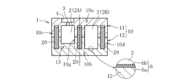
- FIG. 5A to 5C conceptually show a partial plan view, a transverse sectional view, and a longitudinal sectional view of a waveguide slot antenna 1 according to a third embodiment of the first invention.
- a radiation slot array in which a plurality of radiation slots 3 are arranged at predetermined intervals along the tube axis direction is provided in the width direction of the waveguide 10. Two rows are provided, and the arrangement positions of the radiation slots 3 constituting one radiation slot row and the radiation slots 3 constituting the other radiation slot row are different from each other in the tube axis direction.
- a plurality of radiation slots 3 and depressions 4 are arranged in a staggered manner.
- the waveguide slot antenna 1 (waveguide 10) of this embodiment is disposed in parallel with the side walls 10c and 10d, and the waveguide 2 is divided into two waveguides 2A. , 2B and a plurality of inner walls 13 for reducing the cross-sectional area of the waveguide 2 (2A, 2B) at the position where the radiation slot 3 is formed.
- the inner wall 13 is erected on the inner bottom surface of the bottom wall 10b. Of the two inner walls 13, 13 adjacent in the tube axis direction, the height dimension of the inner wall 13 on the side relatively closer to the power supply slot 5 is h 1.
- the inner wall 13 When the height dimension of the inner wall 13 relatively far from the power supply slot 5 is h 2 , the inner wall 13 is formed so as to satisfy the relational expression h 1 ⁇ h 2 (see the enlarged view in FIG. 5C).
- One radiation slot row is formed along the waveguide 2A, and the other radiation slot row is formed along the waveguide 2B.
- the inner wall 13 for reducing the cross-sectional area of the waveguide 2 is provided at the position where the radiation slot 3 is formed, the radiation efficiency of the radio wave propagating through the waveguide 2 can be increased.
- the height dimension of the inner wall 13 on the side relatively close to the power supply slot 5 is h 1
- the inner wall 13 on the side relatively far from the power supply port 5 is.
- the waveguide 10 constituting the waveguide slot antenna 1 of this embodiment also has an end-like cross section at each portion in the extending direction of the waveguide 2, and at least the defined surface of the waveguide 2 is the conductive coating 6.
- the first and second waveguide-forming members 11 and 12 made of resin covered with are joined together. Specifically, a first wall 10a provided with the radiating slot 3 and the depression 4 and a side wall 10c, 10d, an end wall 10e, 10f, and a part of the branch wall 10g (upper part) are integrated.
- the waveguide 10 is formed by coupling with the wave tube forming member 12.
- the waveguide slot antenna 1 of this embodiment also has a cored bar 20 that is disposed along the tube axis direction and is held by both the first and second waveguide forming members 11 and 12.
- the cored bar 20 is made of a rectangular (rectangular) plate-like member extending in the tube axis direction, and is embedded in the side walls 10c and 10d and the branch wall 10g in a standing posture.
- the first and second waveguide forming members 11 and 12 can be injection-molded with resin using the insert 20 as an insert component, and the two cores 20 and 20 held by the side walls 10c and 10d are used as insert components. Either one of the wave tube forming members 11 and 12 is injection-molded with resin, and the other one of the waveguide forming members 11 and 12 is injection-molded with resin using the cored bar 20 held by the branch wall 10g as an insert part. You can also
- FIG. 6A shows a schematic cross-sectional view of a waveguide slot antenna A according to the fourth embodiment of the first invention.
- a waveguide slot antenna 1 shown in the figure is a modification of the waveguide slot antenna 1 shown in FIGS. 5A to 5C, and the branch wall 10g is connected to the first and second waveguide forming members 11 and 12. Only formed with. That is, the branch wall 10g does not hold the cored bar 20.
- the concave portion provided in the portion where the branch wall 10g of the first waveguide forming member 11 is formed is provided in the portion where the branch wall 10g of the second waveguide forming member 12 is formed.
- a branch wall 10g is formed by fitting (press-fitting) the convex portions.
- FIG. 6B shows a schematic cross-sectional view of the waveguide slot antenna 1 according to the fifth embodiment of the first invention.
- a waveguide slot antenna 1 shown in the figure is a modification of the waveguide slot antenna 1 shown in FIGS. 5A to 5C, and includes a core metal 20 held by a side wall 10c and a surface of the core metal 20 held by a side wall 10d. Are exposed on the outer surface of the waveguide 10. Although illustration is omitted, the same configuration may be adopted in the waveguide slot antenna 1 shown in FIGS.
- the waveguide slot antenna 1 according to the embodiment of the first invention of the present application described above has a feature that it is possible to prevent deformation due to a temperature change or the like as much as possible. Therefore, in the first invention of the present application, among the waveguide slot antennas, in particular, it is necessary to increase the antenna size (increase in the tube axis direction) in relation to the wavelength, and deformation due to temperature change or the like is required.
- the present invention can be preferably applied to a waveguide slot antenna for transmitting and receiving radio waves in a low frequency band that are easily generated.
- FIG. 7A is a sectional view taken along line Y1-Y1 in FIG. 7A.
- the waveguide slot antenna 31 shown in FIG. 7A is used as a member constituting an antenna unit for transmitting and receiving millimeter wave radio waves, for example.
- the antenna unit includes a plurality of (for example, five) waveguide slot antennas 31 connected in parallel, and a power supply that supplies high-frequency power (radio waves) to each of the waveguide slot antennas 31.
- this waveguide slot antenna 31 When this waveguide slot antenna 31 is used for transmitting and receiving millimeter-wave band (eg, 76 GHz band) radio waves, the size is, for example, the dimension in the tube axis direction (up and down direction in the drawing of FIG. 7A): 90 mm, dimension in the width direction (left and right direction in FIG. 7A): 7 mm, and dimension in the height direction (direction perpendicular to the sheet surface in FIG. 7A): 7 mm.
- millimeter-wave band eg, 76 GHz band
- the waveguide slot antenna 31 includes a waveguide 40 having a waveguide 32 extending in the tube axis direction and a predetermined interval along the tube axis direction of the waveguide 40. And a feed slot 35 that is provided at one end in the tube axis direction of the waveguide 40 and supplies high-frequency power (radio waves) to the waveguide 32.
- the radiation slot 33 of the present embodiment is provided such that a straight line extending through the center in the width direction is inclined by 45 ° with respect to the tube axis direction.
- the inclination angle 33 can be set as appropriate according to the application.
- the waveguide 40 is a rectangular waveguide having a rectangular cross section at each portion in the extending direction of the waveguide 32. More specifically, it includes a top wall 40a and a bottom wall 40b that are parallel to each other, side walls 40c and 40d that are parallel to each other, and further includes end walls 40e and 40f that close one end and the other end opening in the tube axis direction. .
- the plurality of radiation slots 33 are provided in the top wall 40a, and the power feeding slot 35 is provided in the bottom wall 40b.
- the cross-sectional dimensions of the top wall 30a and the bottom wall 30b are longer than the cross-sectional dimensions of the side walls 30c and 30d.
- the side on which the top wall 40a is provided is referred to as the upper side, and the side on which the bottom wall 40b is provided is referred to as the lower side, but the usage mode of the waveguide slot antenna 31 is not limited. .
- the top wall 40a is provided on the front side in the radiation direction of the radio wave radiated to the outside through the radiation slot 33, and has a hole 34 in which the radiation slot 33 is disposed on the inner periphery. That is, the top wall 40 a is provided with a plurality of holes 34 opened on the outer surface (upper surface) thereof along the tube axis direction, and one radiation slot 33 is opened on the inner bottom surface of each hole 34.
- the hole portion 34 is formed in a perfect circle shape in plan view, but the hole portion 34 can also be formed in a rectangular shape, an elliptical shape, or the like in plan view. By providing such a hole 34, unnecessary radiation, also referred to as a grating lobe, is suppressed, so that the antenna characteristics can be improved.
- the waveguide 40 is composed of a combined body of first and second waveguide forming members 41 and 42 whose end sections are cross sections in the extending direction of the waveguide 32. Specifically, as shown in FIGS. 7B and 7C, the first waveguide forming member 41 constituting the top wall 40a, the bottom wall 40b, the side walls 40c and 40d, and the end walls 40e and 40f are integrally formed.
- Combined body with the second waveguide forming member 42 that is, the first waveguide forming member 41 having a flat plate shape, and the second waveguide forming having a concave shape with the transverse section opened upward.
- the waveguide 40 is configured by a combination with the member 42.
- the first waveguide forming member 41 includes, for example, a first metal plate 41A formed in a predetermined shape by pressing (punching) a metal plate, and pressing (punching) the metal plate. It is comprised by the laminated body with the 2nd metal plate 41B formed in the predetermined shape by giving.
- the radial slot 33 is formed at the same time as the first metal plate 41A is obtained by pressing, and the hole 34 is formed at the same time as the second metal plate 41B is obtained by pressing.
- the second waveguide forming member 42 is a resin member integrally holding the first waveguide forming member 41, that is, the first waveguide forming member 41 is inserted and injection molded with resin.
- the power supply slot 35 is molded at the same time as the injection molding.
- the resin material used for molding the second waveguide forming member 42 is based on, for example, at least one thermoplastic resin selected from the group of liquid crystal polymer (LCP), polyphenylene sulfide (PPS), and polyacetal (POM).
- LCP liquid crystal polymer
- PPS polyphenylene sulfide
- POM polyacetal
- a resin added with one or more fillers such as glass fiber (GF) and carbon fiber (CF) is used as necessary.
- GF glass fiber
- CF carbon fiber
- LCP is preferable in that it has excellent shape stability compared to PPS and the like and can suppress the amount of burrs generated during molding.
- the second waveguide forming member 42 has a holding portion 42a that integrally holds the first waveguide forming member 41.
- This holding part 42a is arranged as an insert part in the molding die in a state where both the metal plates 41A and 41B are stacked, and then the above resin material is filled in the filling part (hole part) 37 provided in both the metal plates 41A and 41B.
- the second waveguide forming member 42 is obtained by injection molding so as to be filled.
- the holding portions 42a are provided only at both ends (terminal walls 40e, 40f) in the tube axis direction, but it is of course possible to provide the holding portions 42a on the side walls 40c, 40d. Is possible.
- the holding portion 42a is formed by a method other than the above, for example, by combining and integrating the two metal plates 41A and 41B by an appropriate means such as adhesion or welding, and then this integrated product (first waveguide forming member 41). Is inserted into the molding die as an insert part, and then the second waveguide forming member 42 is filled with the resin material in the plurality of filling portions 37 provided only on the first metal plate 41A. It can also be obtained by injection molding (see FIG. 8B). The configuration shown in FIG. 8B is preferably obtained as described above from the viewpoint of suppressing the deformation of the second waveguide forming member 42 due to molding shrinkage, but only the first metal plate 41A is an insert component. Alternatively, after the second waveguide forming member 42 is injection-molded with a resin, the second metal plate 41B can be joined to the first metal plate 41A by an appropriate means.
- a conductive coating 36 is not interrupted at the contact portion (boundary portion) between the two waveguide forming members 41 and 42, and the surface defining the waveguide 32 of the first waveguide forming member 41, and the first The two waveguide forming members 42 are continuous on the surface defining the waveguide 32.
- a conductive coating 36 is obtained by obtaining the waveguide 40 as described above, and then subjecting the waveguide 40 to a treatment for forming the conductive coating 36, specifically, an electroless plating treatment. It is obtained with.
- the conductive coating 36 may be formed on the outer surface of the waveguide 40 (the entire surface of the waveguide 40) in addition to the surface defining the waveguide 32.
- Such a configuration can be obtained by applying the conductive film 36 to the waveguide 40 without subjecting the waveguide 40 to the masking process.
- the masking process for the waveguide 40 can be omitted, which is advantageous in reducing the cost required for forming the conductive coating 36 and, consequently, the manufacturing cost of the waveguide slot antenna 31.
- the conductive coating 36 may be composed of a single-layer metal plating coating, but here, the first coating 36a deposited on the waveguide 40 and the second deposited on the first coating 36a.
- the conductive film 36 is composed of the film 36b.
- the first coating 36a can be a plated plating of metal such as copper, silver, gold, etc., which is particularly excellent in conductivity (propagation of radio waves), and the second coating 36b can be made of a durable (anti-resistance) such as nickel. It is possible to obtain a metal plating film having excellent corrosion resistance.
- the conductive coating 36 have such a laminated structure, high conductivity and high durability can be simultaneously imparted to the conductive coating 36, and the amount of expensive metal such as copper or silver used It is possible to suppress the increase in cost.
- the film thickness of the conductive coating 36 is 0.2 ⁇ m or more and 1.5 ⁇ m or less.
- the film thickness of the first coating 36a and the second coating 36b is, for example, 0.1. It can be about -1.0 ⁇ m and about 0.1-0.5 ⁇ m.
- the waveguide 40 has a first waveguide formation member 41 made of a flat metal member having a plurality of radiation slots 33, and a first waveguide formation. It is composed of a combination of the second waveguide forming members 42 made of a resin member integrally holding the member 41, and at least the defined surface of the waveguide 32 of the waveguide 40 is continuous conductive. It is covered with a coating 36.
- the first waveguide forming member 41 made of a flat metal member is inserted, and the second waveguide forming member 42 is injection-molded with resin.
- the waveguide 40 can be obtained, and then the conductive film 36 can be formed on the waveguide 40.
- the first waveguide forming member 41 made of metal is inserted and the second waveguide forming member 42 is injection-molded with resin, the first waveguide 40 is obtained. Since the waveguide forming member 41 can function as a reinforcing member, the second waveguide forming member 42 is prevented from being deformed due to molding shrinkage as much as possible, and the deformation due to temperature change or the like occurs. The difficult waveguide 40 can be obtained at low cost.
- the second waveguide forming member 42 that is inserted and molded with resin by inserting the first waveguide forming member 41 includes a holding portion 42a that integrally holds the first waveguide forming member 41.
- the propagation efficiency of the radio wave is reduced due to the reduction in the shape accuracy of the waveguide 40 (waveguide 32), and the contact between the waveguide forming members 41 and 42 is further reduced.
- the possibility of occurrence of problems that deteriorate the antenna characteristics, such as external leakage of radio waves through a gap generated in the section, is reduced as much as possible.
- the waveguide slot antenna 31 which can exhibit a desired antenna characteristic stably is realizable.
- the waveguide slot antenna 31 according to the first embodiment of the second invention of the present application has been described above.
- the waveguide slot antenna 31 may be appropriately changed without departing from the gist of the present invention. It is possible to apply.
- other embodiments of the second invention will be described with reference to the drawings. However, configurations similar to those of the first embodiment described above are denoted by common reference numerals, and redundant description is omitted.
- FIGS. 9A and 9B conceptually show a transverse sectional view and a longitudinal sectional view of a waveguide slot antenna 31 according to a second embodiment of the second invention, respectively.
- the main difference between the waveguide slot antenna 31 shown in the figure and the waveguide slot antenna 31 described above is that a holding portion 42a for holding the first waveguide forming member 31 integrally is provided.
- the second waveguide forming member 42 is endlessly formed along the outer periphery of the upper end, that is, along the outer periphery of the upper ends of the side walls 40c and 40d and the end walls 40e and 40f. Even when such a configuration is employed, the same operational effects as those of the waveguide slot antenna 31 according to the first embodiment can be obtained.
- 10A to 10C a partial plan view, a transverse cross-sectional view (cross-sectional view taken along line X2-X2 in FIG. 10A), and a vertical cross-sectional view (FIG. 10) of the waveguide slot antenna 31 according to the third embodiment of the second invention.
- 10A conceptually shows a sectional view taken along line Y2-Y2 in FIG.
- a radiation slot array in which a plurality of radiation slots 33 are arranged at predetermined intervals along the tube axis direction is provided in the width direction of the waveguide 40.
- the arrangement positions of the radiation slots 33 constituting one radiation slot row and the radiation slots 33 constituting the other radiation slot row are different from each other in the tube axis direction.
- a plurality of radiation slots 33 and a plurality of holes 34 are arranged in a staggered manner.
- the waveguide slot antenna 31 (waveguide 40) of this embodiment is disposed in parallel with the side walls 40c and 40d, and the waveguide 32 is divided into two waveguides 32A. , 32B and a plurality of inner walls 43 that reduce the cross-sectional area of the waveguide 32 (32A, 32B) at the position where the radiation slot 33 is formed.
- the inner wall 43 is erected on the inner bottom surface of the bottom wall 40b. Of the two inner walls 43, 43 adjacent in the tube axis direction, the height dimension of the inner wall 43 closer to the power supply slot 35 is set to h 10.
- One radiating slot row is formed along the waveguide 32A, and the other radiating slot row is formed along the waveguide 32B.
- the inner wall 43 that reduces the cross-sectional area of the waveguide 32 is provided at the position where the radiation slot 33 is formed, the radiation efficiency of radio waves propagating through the waveguide 32 can be increased.
- the height dimension of the inner wall 43 on the side relatively close to the power supply slot 35 is h 10
- the inner wall 43 on the side relatively far from the power supply port 35 is.
- the first waveguide forming member 41 made of a flat metal member and the first waveguide forming member 41 are integrally formed.
- a resin-made second waveguide forming member 41 injection-molded by inserting the first waveguide forming member 41, and at least the defining surface of the waveguide 32 is Covered with a continuous conductive coating 36.
- FIG. 11 is a schematic cross-sectional view of a waveguide slot antenna 31 according to the fourth embodiment of the second invention.
- a waveguide slot antenna 31 shown in the figure is a modification of the waveguide slot antenna 31 shown in FIGS. 7A to 7C, and the first waveguide forming member 31 is a single flat metal member.
- the configuration differs from the waveguide slot antenna 31 shown in FIG. 7A and the like. Although not shown, it is of course possible to apply the configuration of this embodiment to the waveguide slot antenna 31 shown in FIGS. 9A and 10A.
- the second invention of the present application described above can be applied to the centimeter wave (low frequency band) radio wave in addition to the waveguide slot antenna 31 for transmitting and receiving millimeter wave (high frequency band) radio waves.
- the present invention can be applied to a waveguide slot antenna for transmitting and receiving.
Landscapes
- Engineering & Computer Science (AREA)
- Manufacturing & Machinery (AREA)
- Waveguide Aerials (AREA)
Abstract
管軸方向に延びた導波路2を有する樹脂製の導波管10と、導波管10に設けられた複数の放射スロット3とを備えた導波管スロットアンテナ1であって、導波管10が、導波路2の延在方向各部における横断面が有端状をなし、相手側と結合されることで導波路2を画成する第1および第2の導波管形成部材11,12からなるものにおいて、管軸方向に沿って配置された芯金20を有し、芯金20が、両導波管形成部材11,12に保持されている。
Description
本発明は、導波管スロットアンテナおよびその製造方法に関する。
周知のように、導波管スロットアンテナは、無線通信機能を備えた種々の電気・電子機器(システム)において、高周波帯域の電波(例えばミリ波帯の電波)や、低周波帯域の電波(例えばセンチメートル波帯の電波)を送受信するためのアンテナとして使用されている。ミリ波帯の電波は、例えば車載用レーダシステムで利用され、センチメートル波帯の電波は、例えば、放送衛星(BS)や通信衛星(CS)などによる衛星放送システム、無線LANやBluetooth(登録商標)などのデータ伝送システム、ETC(登録商標)と略称される電子料金収受システムなどで利用されている。なお、ミリ波帯の電波とは、波長1~10mm、周波数30~300GHzの電波であり、センチメートル波帯の電波とは、波長10~100mm、周波数3~30GHzの電波である。
無線通信機能を備えた各種システムの低価格化を推進すべく、導波管スロットアンテナのコスト低減を図る必要が生じている。そこで、本出願人は、下記の特許文献1において、樹脂製の導波管スロットアンテナを提案している。より具体的には、管軸方向に延びた導波路を有し、導波路の画成面が導電性被膜で被覆された樹脂製の導波管と、該導波管に、その管軸方向に沿って所定間隔で設けられた複数の放射スロットとを備え、導波管が、横断面(管軸方向と直交する断面)が有端状をなし、相手側と結合されることで導波路を画成する第1および第2の導波管形成部材で構成された導波管スロットアンテナである。
ところで、特に低周波数帯域の電波を送受信する用途では、波長との関係でアンテナサイズを大きくする(アンテナを長寸化する)必要があるが、特許文献1に記載の導波管スロットアンテナにおいて、そのサイズを大きくした場合、温度変化等に伴って導波管(両導波管形成部材の何れか一方又は双方)に望まない変形、例えば、管軸方向の反りや曲りが生じ易い。そして、上記のような変形が生じると、
・導波路の形状精度に悪影響が及び、電波の伝搬効率が低下する、
・両導波管形成部材の結合部に隙間が生じ、この隙間を介して導波路を伝搬する電波が外部に漏れ易くなる、
などといった不具合が生じ易くなることから、所望のアンテナ特性を安定的に発揮することができなくなる。
・導波路の形状精度に悪影響が及び、電波の伝搬効率が低下する、
・両導波管形成部材の結合部に隙間が生じ、この隙間を介して導波路を伝搬する電波が外部に漏れ易くなる、
などといった不具合が生じ易くなることから、所望のアンテナ特性を安定的に発揮することができなくなる。
以上の実情に鑑み、本発明の目的は、所望のアンテナ特性を安定的に発揮することのできる導波管スロットアンテナを実現することにある。
上記の目的を達成するために創案された本願の第1発明は、管軸方向に延びた導波路を有し、導波路の画成面が導電性被膜で被覆された樹脂製の導波管と、導波管の管軸方向に沿って所定間隔で設けられた複数の放射スロットとを備えた導波管スロットアンテナであって、導波管が、導波路の延在方向各部における横断面が有端状をなし、相手側と結合されることで導波路を画成する第1および第2の導波管形成部材で構成されるものにおいて、管軸方向に沿って配置された芯金を有し、この芯金が、第1および第2の導波管形成部材の双方に保持されていることを特徴とする。
上記のように、第1および第2の導波管形成部材の双方で、管軸方向に沿って配置された芯金(管軸方向に延びる芯金)を保持しておけば、両導波管形成部材の結合体からなる導波管の曲げ剛性やねじり剛性を高めることができるので、温度変化等に伴う導波管の変形(特に管軸方向に沿う方向の反り・曲がり)が生じ難くなる。このため、上述のような不具合が生じる可能性を可及的に減じ、所望のアンテナ特性を安定的に発揮することのできる導波管スロットアンテナを実現することができる。
第1および第2の導波管形成部材の少なくとも一方を、芯金を一体的に有する樹脂の射出成形品(芯金をインサート部品とした樹脂の射出成形品)とすることができる。このようにすれば、少なくとも上記一方の成形収縮に伴う変形も可及的に防止することができる。このため、成形収縮に伴う変形に起因した導波管形成部材同士の結合精度の低下等も可及的に防止することが可能となり、これを通じて、アンテナ特性に優れた導波管スロットアンテナを安定的に得ることができる。
芯金を、第1の芯金と第2の芯金の結合体で構成し、第1の導波管形成部材を、第1の芯金を一体的に有する樹脂の射出成形品(第1の芯金をインサート部品とした樹脂の射出成形品)で構成すると共に、第2の導波管形成部材を、第2の芯金を一体的に有する樹脂の射出成形品(第2の芯金をインサート部品とした樹脂の射出成形品)で構成するようにしても良い。このようにすれば、第1および第2の導波管形成部材の双方について、その成形収縮に伴う変形を可及的に防止することができるので、一層アンテナ特性に優れた導波管スロットアンテナを安定的に得ることができる。
芯金は、導波管の壁部内に埋設しても良いし、その一部を導波管の外表面に露出させても良い。
第1および第2の導波管形成部材は、何れも、上記横断面が凹形状をなすものとすることができる。
また、上記の目的を達成するために創案された本願の第2発明は、管軸方向に延びた導波路を有する導波管と、導波管の管軸方向に沿って所定間隔で設けられた複数の放射スロットとを備え、導波管が、導波路の延在方向各部における横断面が有端状をなした第1および第2の導波管形成部材の結合体で構成された導波管スロットアンテナにおいて、第1の導波管形成部材が、複数の放射スロットを有する平板状の金属部材で構成されると共に、第2の導波管形成部材が、第1の導波管形成部材を一体的に保持した樹脂部材で構成され、かつ導波管のうち、少なくとも導波路の画成面が、連続した導電性被膜で被覆されていることを特徴とする。
上記構成を有する導波管スロットアンテナは、複数の放射スロットを有する平板状の金属部材からなる第1の導波管形成部材をインサートして第2の導波管形成部材を樹脂で射出成形することによって導波管を得、その後、この導波管に対して少なくとも導波路の画成面を被覆する導電性被膜の形成処理を実行することで製造することができる。
上記のように、平板状の金属部材で構成された第1の導波管形成部材をインサートして第2の導波管形成部材を樹脂で射出成形することによって導波管を得るようにすれば、第1の導波管形成部材を補強部材として機能させることができるので、成形収縮に伴う第2の導波管形成部材の変形(特に管軸方向の反り・曲り)を可及的に防止しつつ、温度変化等に伴う変形が生じ難い導波管を低コストに得ることができる。また、第2の導波管形成部材が第1の導波管形成部材を一体的に保持していること、および、両導波管形成部材の結合体からなる導波管のうち、少なくとも導波路の画成面が連続した導電性被膜(切れ目のない導電性被膜)で被覆されていることにより、両導波管形成部材の結合部に、導波路を伝搬する電波が外部に漏れ出すような隙間が形成されるのを効果的に防止することができる。以上のことから、所望のアンテナ特性を安定的に発揮することのできる導波管スロットアンテナを低コストに実現することができる。
第2発明の構成において、第1の導波管形成部材は、放射スロットを介して外部に放射される電波の放射方向前方側に設けられ、放射スロットを内周に配置した孔部をさらに有するものとすることができる。このような孔部を設けておけば、グレーティングローブとも称される不要放射を排除することができるので、導波管スロットアンテナのアンテナ特性を高めることができる。
この場合、第1の導波管形成部材は、放射スロットを有する第1の金属板と、上記孔部を有する第2の金属板との積層体で構成することができる。このようにすれば、放射スロットを有する第1の金属板および上記孔部を有する第2の金属板のそれぞれを、金属板にプレス加工(打ち抜き加工)を施すことで得られるプレス成形品とすることができるので、放射スロットおよび孔部を有する第1の導波管形成部材を低コストに作製することができる。
導電性被膜は、導波管の外表面に沿って連続的に形成することもできる。このような導電性被膜(導波管)は、マスキング処理を施さずに導波管に対して導電性被膜の形成処理を施すことで得られる。このようにすれば、導波管に対するマスキングの形成処理を省略することができるので、導波管スロットアンテナのコスト低減を図る上で有利となる。
以上に示すように、本願の第1および第2発明によれば、所望のアンテナ特性を安定的に発揮することのできる導波管スロットアンテナを実現することができる。
以下、本発明の実施の形態を、図面を参照しながら説明する。
図1Aおよび図1Bに、導波管スロットアンテナ1を備えたアンテナユニットAの概略平面図及び概略背面図をそれぞれ示す。このアンテナユニットAは、センチメートル波帯の電波を送受信するためのものであって、並列に接続された複数本(図示例では5本)の導波管スロットアンテナ1と、各導波管スロットアンテナ1に高周波電力(電波)を供給する給電導波管9(図1B中に二点鎖線で示す)とを備える。導波管スロットアンテナ1を並列に接続するための手段に特段の限定はなく、例えば、接着、両面テープ止め、凹凸嵌合などの固定手段を単独で、あるいは二種以上組み合わせることができる。5本の導波管スロットアンテナ1のうち、例えば中央部に配置されたアンテナ1は電波の送信用アンテナとして機能させることができ、その両側に2本ずつ配置されたアンテナ1は電波の受信用アンテナとして機能させることができる。なお、このアンテナユニットAを24GHz帯の電波を送受信するための用途に用いる場合、各導波管スロットアンテナ1のサイズは、例えば、管軸方向(図1Aの紙面上下方向)の寸法:100mm、幅方向(図1Aの紙面左右方向)の寸法:20mm、高さ方向(図1Aにおいて紙面と直交する方向)の寸法:5mm、とされる。
次に、各導波管スロットアンテナ1の詳細構造を説明する。導波管スロットアンテナ1は、図2Aおよび図2Bにも示すように、内部に管軸方向に延びた導波路2を有する導波管10と、導波管10の管軸方向に沿って所定間隔で設けられた複数の放射スロット3と、導波管10の管軸方向の一端に設けられ、導波路2に高周波電力を供給する給電スロット5と、を備える。図1Aに示すように、本実施形態の放射スロット3は、その幅方向中央部を通って延びる直線が管軸方向に対して45°傾くように設けられているが、管軸方向に対する放射スロット3の傾斜角は、用途等に応じて適宜設定することができる。
図2Aおよび図2Bに示すように、導波管10は、導波路2の延在方向各部における横断面が方形状をなす方形導波管とされる。より具体的には、互いに平行な頂壁10aおよび底壁10bと、互いに平行な側壁10c,10dとを備え、さらに、管軸方向の一端および他端開口を閉塞する終端壁10e,10fを備える。複数の放射スロット3は頂壁10aに設けられ、給電スロット5は底壁10bに設けられている。本実施形態において、頂壁10aおよび底壁10bの横断面寸法は、側壁10c,10dの横断面寸法よりも長寸とされる。なお、以下では、説明の便宜上、頂壁10aが設けられた側を上側、底壁10bが設けられた側を下側とも言うが、導波管スロットアンテナ1の使用態様を限定するわけではない。
頂壁10aには、その外表面に開口した窪み部4が管軸方向に沿って複数設けられ、各窪み部4の内底面に一の放射スロット3が開口している。本実施形態では、窪み部4を平面視で真円状に形成しているが、窪み部4は、平面視で矩形状、楕円状等に形成することもできる。このような窪み部4を設けることにより、グレーティングローブとも称される不要放射が抑制される。
導波管10は、導波路2の延在方向各部における横断面が有端状をなす第1および第2の導波管形成部材11,12を結合することで形成される。具体的には、図2Aに示すように、放射スロット3が設けられた頂壁10aと、側壁10c,10dおよび終端壁10e,10fの一部(上側部分)とを一体に有する第1の導波管形成部材11と、給電スロット5が設けられた底壁10bと、側壁10c,10dおよび終端壁10e,10fの残部(下側部分)とを一体に有する第2の導波管形成部材12とを結合することで導波管10が形成される。要するに、本実施形態の導波管10は、上記横断面が下側に開口した凹形状をなす第1の導波管形成部材11と、上記横断面が上側に開口した凹形状をなす第2の導波管形成部材12とを結合することで形成される。
第1の導波管形成部材11は、樹脂の射出成形品とされ、射出成形と同時に放射スロット3および窪み部4が型成形される。また、第2の導波管形成部材12も樹脂の射出成形品とされ、射出成形と同時に給電スロット5が型成形される。導波管形成部材11,12の成形用樹脂としては、例えば、液晶ポリマー(LCP)、ポリフェニレンサルファイド(PPS)およびポリアセタール(POM)の群から選択される少なくとも一種の熱可塑性樹脂をベース樹脂としたものが使用され、ベース樹脂には、必要に応じて、グラスファイバー(GF)やカーボンファイバー(CF)等の充填材が一種又は複数種添加される。以上で例示した樹脂の中でも、LCPは、PPS等に比べて形状安定性に優れ、かつ成形に伴うバリの発生量を抑制し得る点で好ましい。
第1の導波管形成部材11のうち導波路2を画成する面、および第2の導波管形成部材12のうち導波路2を画成する面は、図2A中の拡大図に示す導電性被膜6で被覆されている。これにより、導波路2に沿って電波を円滑に伝播させることができる。なお、導電性被膜6は、両導波管形成部材11,12の表面全域に形成しても構わない。このようにすれば、導電性被膜6の形成前におけるマスキングの形成作業と、導電性被膜6の形成後におけるマスキングの除去作業とが不要となるので、被膜形成コスト、ひいては導波管スロットアンテナ1の製造コストを抑えることができる。
導電性被膜6は、単層の金属メッキ被膜で構成しても構わないが、ここでは、導波管形成部材11,12に析出形成した第1被膜6aと、この第1被膜6a上に析出形成した第2被膜6bとで導電性被膜6を構成している。第1被膜6aは、銅、銀、金等、特に導電性(電波の伝搬性)に優れた金属のメッキ被膜とすることができ、また、第2被膜6bは、ニッケル等、耐久性(耐腐食性)に優れた金属のメッキ被膜とすることができる。導電性被膜6をこのような積層構造とすることにより、導電性被膜6に高い導電性と高い耐久性とを同時に付与することができることに加え、高価な金属である銅や銀等の使用量を抑えてコスト増を抑制することができる。
導電性被膜6(6a,6b)は、例えば、電解メッキ法や無電解メッキ法で形成することができるが、無電解メッキ法の方が好ましい。無電解メッキ法の方が、電解メッキ法よりも均一厚みの導電性被膜6(6a,6b)を得易いため、所望のアンテナ特性を確保する上で有利となるからである。導電性被膜6の膜厚は、これが薄過ぎると耐久性に乏しくなり、逆に厚過ぎると被膜形成に多大な時間を要してコスト高を招来する。かかる観点から、導電性被膜6の膜厚は0.2μm以上1.5μm以下とするのが好ましい。なお、本実施形態のように、導電性被膜6を第1被膜6aと第2被膜6bの積層構造とする場合、第1被膜6aおよび第2被膜6bの膜厚は、それぞれ、例えば0.1~1.0μm程度および0.1~0.5μm程度とすることができる。
導波管10は、管軸方向に沿って配置され、第1および第2の導波管形成部材11,12の双方に保持された芯金20をさらに有する。芯金20は、図3Aにも示すように、管軸方向に延びる矩形状(長方形状)の板状部材からなり、起立姿勢で側壁10c,10dの内部にそれぞれ埋設されている。すなわち、本実施形態において、一対の芯金20,20は、導波管10の内側面(導波路2)および外側面の何れにも露出していない。芯金20は、例えば、ステンレス鋼、黄銅、アルミニウム(アルミニウム合金)等の金属板の他、鉄又は銅を主成分とする焼結金属製の板状部材を採用することができる。なお、導波路2を伝搬する電波の伝搬性を一層高めるため、芯金20としては、導電性に優れた黄銅板やアルミニウム板を採用するのが特に好ましい。
一対の芯金20,20は、例えば、以下の(1)~(3)に示す何れかの手段(手順)を採用することにより、第1および第2導波管形成部材11,12の双方で保持することができる。
(1)芯金20,20の上側部分を第1の導波管形成部材11(の側壁10c,10dを構成する部分)に設けた保持部11aに嵌合すると共に、芯金20,20の下側部分を第2の導波管形成部材12(の側壁10c,10dを構成する部分)に設けた保持部12aに嵌合する(図3Aを参照)。
(2)芯金20,20の下側部分を第2の導波管形成部材12で一体的に保持するように、芯金20,20をインサート部品として第2の導波管形成部材12を樹脂で射出成形してから、芯金20,20の上側部分(第2の導波管形成部材12から突出した部分)を第1の導波管形成部材11の側壁10c,10dを構成する部分にそれぞれ設けた保持部11aに嵌合する(図3Bを参照)。
(3)芯金20,20の上側部分を第1の導波管形成部材11で一体的に保持するように、芯金20,20をインサート部品として第1の導波管形成部材11を樹脂で射出成形してから、芯金20,20の下側部分(第1の導波管形成部材11から突出した部分)を第2の導波管形成部材12の側壁10c,10dを構成する部分にそれぞれ設けた保持部12aに嵌合する(図3Cを参照)。
(1)芯金20,20の上側部分を第1の導波管形成部材11(の側壁10c,10dを構成する部分)に設けた保持部11aに嵌合すると共に、芯金20,20の下側部分を第2の導波管形成部材12(の側壁10c,10dを構成する部分)に設けた保持部12aに嵌合する(図3Aを参照)。
(2)芯金20,20の下側部分を第2の導波管形成部材12で一体的に保持するように、芯金20,20をインサート部品として第2の導波管形成部材12を樹脂で射出成形してから、芯金20,20の上側部分(第2の導波管形成部材12から突出した部分)を第1の導波管形成部材11の側壁10c,10dを構成する部分にそれぞれ設けた保持部11aに嵌合する(図3Bを参照)。
(3)芯金20,20の上側部分を第1の導波管形成部材11で一体的に保持するように、芯金20,20をインサート部品として第1の導波管形成部材11を樹脂で射出成形してから、芯金20,20の下側部分(第1の導波管形成部材11から突出した部分)を第2の導波管形成部材12の側壁10c,10dを構成する部分にそれぞれ設けた保持部12aに嵌合する(図3Cを参照)。
なお、本実施形態では、上記(2)の手段を採用することにより、一対の芯金20,20を両導波管形成部材11,12で保持している。ここで、上記(2)の手段を採用する場合において、第1の導波管形成部材11に設けた保持部11aの上下方向寸法が、この保持部11aで保持すべき芯金20の上側部分の上下方向寸法よりも小さいと、第1の導波管形成部材11と第2の導波管形成部材12の対向二面を当接させることができない(両導波管形成部材11,12間に隙間が生じる)ため、アンテナ特性に悪影響が及ぶ可能性がある。そのため、保持部11aの上下方向寸法は、この保持部11aで保持すべき芯金20の上側部分の上下方向寸法よりも僅かに大きく設定しておく。上記(1)又は(3)の手段を採用する場合においても、同様の理由から、保持部11a,12aの上下方向寸法を設定する。
以上から、本実施形態に係る導波管スロットアンテナ1(導波管10)は、第1の導波管形成部材11を樹脂で射出成形すると共に、芯金20,20をインサート部品として第2の導波管形成部材12を樹脂で射出成形してから、両導波管形成部材11,12の導波路2を画成する面に導電性被膜6を形成し、その後、両導波管形成部材11,12を結合することで完成する。第1の導波管形成部材11と第2の導波管形成部材12の結合方法は任意であり、例えば、両導波管形成部材11,12の当接部に塗布した接着剤を硬化させる接着や、両導波管形成部材11,12の当接部において、導波管形成部材11,12同士を溶着させる溶着などを採用することができる。この他にも、両導波管形成部材11,12の何れか一方に設けた凹部に対し、他方に設けた凸部を嵌合(圧入)することにより、両導波管形成部材11,12を結合することもできる。また、芯金20を利用して両導波管形成部材11,12を結合することも可能である。具体的には、例えば、芯金20の上側部分を第1の導波管形成部材11に設けた保持部11aに対して圧入(しまりばめの状態で嵌合)する、接着剤を充填した保持部11aに対して芯金20の上側部分を嵌合した後に接着剤を硬化させる、などを採用することもできる。
なお、両導波管形成部材11,12を結合するのに接着剤を使用する場合、接着剤としては、例えば熱硬化型接着剤、紫外線硬化型接着剤、嫌気性接着剤などを使用することができるが、接着剤を硬化させる際に加熱処理が必要となる熱硬化型接着剤では、加熱処理に伴って、樹脂製の導波管形成部材11,12が変形等する可能性がある。そのため、接着剤としては紫外線硬化型接着剤や嫌気性接着剤が好ましい。なお、接着剤は一般に絶縁体であるので、導波路2の画成面に接着剤が付着すると電波の伝搬性に悪影響が及ぶ可能性がある。そのため、両導波管形成部材11,12を結合するのに接着剤を用いる場合、導波路2の画成面に接着剤が付着しないように注意を払うことが肝要である。
以上で説明した導波管スロットアンテナ1では、第1および第2の導波管形成部材11,12の双方で管軸方向に沿って配置された芯金20を保持している。このようにすれば、導波管10の曲げ剛性やねじり剛性が高まるので、温度変化等に伴って、両導波管形成部材11,12の何れか一方又は双方が変形しようとしても、その変形を芯金20で規制することができる。このため、導波管形成部材11,12の変形により導波路2の形状精度に狂いが生じることで電波の伝搬性が低下する、両導波管形成部材11,12の結合部に隙間が生じ、この隙間を介して導波路2を伝搬する電波が外部に漏れ出す、などといった不具合が生じる可能性を可及的に低減することができる。従って、所望のアンテナ特性を安定的に発揮することのできる導波管スロットアンテナ1を実現することができる。
特に本実施形態では、第2の導波管形成部材12を、芯金20を一体的に有する樹脂の射出成形品(芯金20をインサート部品とした樹脂の射出成形品)としたので、第2の導波管形成部材12については、その成形収縮に伴う変形も可及的に防止することができる。このため、第2の導波管形成部材12の成形収縮に伴う変形に起因した導波管形成部材11,12同士の結合精度の低下等も可及的に防止することが可能となり、これを通じて、アンテナ特性に優れた導波管スロットアンテナ1を安定的に量産することができる。
以上、第1発明の第1実施形態に係る導波管スロットアンテナ1について説明を行ったが、この導波管スロットアンテナ1には適宜の変更を施すことが可能である。以下、他の実施形態について図面を参照しながら説明するが、以上で説明した第1実施形態に準ずる構成には共通の参照番号を付し、重複説明を出来る限り省略する。
図4Aおよび図4Bに、第1発明の第2実施形態に係る導波管スロットアンテナ1の概略斜視図(横断面を含む概略斜視図)を示す。同図に示す導波管スロットアンテナ1が、上述した導波管スロットアンテナ1と異なる主な点は、導波管10の側壁10c,10dのそれぞれに埋設した芯金20を、第1の芯金20Aと第2の芯金20Bとの結合体で構成し、第1の導波管形成部材11を、第1の芯金20Aを一体的に有する樹脂の射出成形品(第1の芯金20Aをインサート部品とした樹脂の射出成形品)で構成すると共に、第2の導波管形成部材12を、第2の芯金20Bを一体的に有する樹脂の射出成形品(第2の芯金20Bをインサート部品とした樹脂の射出成形品)で構成した点にある。
このようにすれば、第1および第2の導波管形成部材11,12の双方について、成形収縮に伴う変形を可及的に防止することができるので、両導波管形成部材11,12の結合精度を一層高めることができる。そのため、一層アンテナ特性に優れた導波管スロットアンテナ1を実現することができる。なお、本実施形態では、図4A,図4Bに示すように、第1の芯金20A(の下端)に設けた凹部に対し、第2の芯金20B(の上端)に設けた凸部を圧入することにより、両芯金20A,20Bの結合体からなる芯金20を実現している。なお、両芯金20A,20Bは、上記の圧入以外にも、例えば、接着、圧入と接着の併用等の手段によって結合させることもできる。また、両導波管形成部材11,12は、任意の方法で結合することができる。
図5A~図5Cのそれぞれに、第1発明の第3実施形態に係る導波管スロットアンテナ1の部分平面図、横断面図および縦断面図を概念的に示す。この実施形態の導波管スロットアンテナ1では、図5Aに示すように、複数の放射スロット3を管軸方向に沿って所定間隔で配置してなる放射スロット列を導波管10の幅方向に二列設けると共に、一方の放射スロット列を構成する放射スロット3と他方の放射スロット列を構成する放射スロット3の管軸方向における配設位置を互いに異ならせている。簡単に言うと、この実施形態の導波管スロットアンテナ1では、放射スロット3および窪み部4が千鳥状に複数配置されている。
また、この実施形態の導波管スロットアンテナ1(導波管10)は、図5Bおよび図5Cに示すように、側壁10c,10dと平行に配設され、導波路2を二条の導波路2A,2Bに分岐させる分岐壁10gと、放射スロット3の形成位置において導波路2(2A,2B)の断面積を縮小させる複数の内壁13とをさらに有する。内壁13は底壁10bの内底面に立設されており、管軸方向で隣り合う2つの内壁13,13のうち、相対的に給電スロット5に近い側の内壁13の高さ寸法をh1、相対的に給電スロット5から遠い側の内壁13の高さ寸法をh2としたとき、h1≦h2の関係式を満たすように形成されている(図5C中の拡大図参照)。一方の放射スロット列は導波路2Aに沿って形成され、他方の放射スロット列は導波路2Bに沿って形成されている。
上記のように、放射スロット3の形成位置において導波路2の断面積を縮小させる内壁13を設けておけば、導波路2を伝搬する電波の放射効率を高めることができる。特に、管軸方向で隣り合う2つの内壁13,13のうち、相対的に給電スロット5に近い側の内壁13の高さ寸法をh1、相対的に給電口5から遠い側の内壁13の高さ寸法をh2としたとき、h1≦h2の関係式を満たすようにすれば、各放射スロット3を介して当該アンテナ1の外部に放射される電波量が放射スロット3相互間でばらつき難くなり、各放射スロット3から概ね等しい量の電波を放射することが可能となる。従って、管軸方向各部でアンテナ性能にばらつきが生じるのを可及的に回避することができ、導波管スロットアンテナ1の信頼性が向上する。
この実施形態の導波管スロットアンテナ1を構成する導波管10も、導波路2の延在方向各部における横断面が有端状をなし、少なくとも導波路2の画成面が導電性被膜6で被覆された樹脂製の第1および第2の導波管形成部材11,12を結合することで形成される。具体的には、放射スロット3および窪み部4が設けられた頂壁10aと、側壁10c,10d、終端壁10e,10fおよび分岐壁10gの一部(上側部分)とを一体に有する第1の導波管形成部材11と、給電スロット5が設けられた底壁10bと、側壁10c,10d、終端壁10e,10fおよび分岐壁10gの残部(下側部分)とを一体に有する第2の導波管形成部材12とを結合することで導波管10が形成される。
また、この実施形態の導波管スロットアンテナ1も、管軸方向に沿って配置され、第1および第2の導波管形成部材11,12の双方に保持された芯金20をさらに有する。芯金20は、管軸方向に延びる矩形状(長方形状)の板状部材からなり、起立姿勢で側壁10c,10dおよび分岐壁10gの内部にそれぞれ埋設されている。上記態様で芯金20を配設したことにより、本実施形態の導波管スロットアンテナ1も、図2等に示す導波管スロットアンテナ1と同様の作用効果を享受することができる。
なお、詳細な図示は省略するが、この実施形態においては、3つの芯金20の全てを両導波管形成部材11,12の何れか一方で一体的に保持するように、3つの芯金20をインサート部品として第1又は第2の導波管形成部材11,12を樹脂で射出成形することができる他、側壁10c,10dでそれぞれ保持される芯金20,20をインサート部品として両導波管形成部材11,12の何れか一方を樹脂で射出成形すると共に、分岐壁10gで保持される芯金20をインサート部品として両導波管形成部材11,12の他方を樹脂で射出成形することもできる。
図6Aに、第1発明の第4実施形態に係る導波管スロットアンテナAの概略横断面図を示す。同図に示す導波管スロットアンテナ1は、図5A~図5Cに示す導波管スロットアンテナ1の変形例であり、分岐壁10gを、第1および第2の導波管形成部材11,12のみで形成している。すなわち、分岐壁10gは芯金20を保持していない。なお、図6Aでは、第1の導波管形成部材11の分岐壁10gを形成する部分に設けた凹部に対し、第2の導波管形成部材12の分岐壁10gを形成する部分に設けた凸部を嵌合(圧入)することにより、分岐壁10gを形成している。
図6Bに、第1発明の第5実施形態に係る導波管スロットアンテナ1の概略横断面図を示す。同図に示す導波管スロットアンテナ1は、図5A~図5Cに示す導波管スロットアンテナ1の変形例であり、側壁10cで保持した芯金20および側壁10dで保持した芯金20の一面を導波管10の外側面に露出させている。図示は省略するが、図2および図4に示す導波管スロットアンテナ1においても同様の構成を採用しても良い。
以上で説明した本願の第1発明の実施形態に係る導波管スロットアンテナ1は、上述したように、温度変化等に伴う変形を可及的に防止することができるという特徴を有する。そのため、本願の第1発明は、導波管スロットアンテナの中でも、特に、波長との関係でアンテナサイズを大きくする(管軸方向に長寸化する)必要があり、温度変化等に伴う変形が生じ易い低周波帯域の電波を送受信するための導波管スロットアンテナに好ましく適用することができる。
図7A~図7Cのそれぞれに、本願の第2発明の第1実施形態に係る導波管スロットアンテナ31の部分平面図、横断面図(図7AのX1-X1線断面図)および縦断面図(図7AのY1-Y1線断面図)を示す。図7Aに示す導波管スロットアンテナ31は、例えば、ミリ波帯の電波を送受信するためのアンテナユニットを構成する部材として使用される。図示は省略するが、上記のアンテナユニットは、並列に接続された複数本(例えば5本)の導波管スロットアンテナ31と、各導波管スロットアンテナ31に高周波電力(電波)を供給する給電導波管とで構成される。なお、この導波管スロットアンテナ31をミリ波帯(例えば76GHz帯)の電波を送受信するための用途に用いる場合、そのサイズは、例えば、管軸方向(図7Aの紙面上下方向)の寸法:90mm、幅方向(図7Aの紙面左右方向)の寸法:7mm、高さ方向(図7Aにおいて紙面と直交する方向)の寸法:7mm、とされる。
次に、導波管スロットアンテナ31の詳細構造を説明する。導波管スロットアンテナ31は、図7A~図7Cに示すように、内部に管軸方向に延びた導波路32を有する導波管40と、導波管40の管軸方向に沿って所定間隔で設けられた複数の放射スロット33と、導波管40の管軸方向の一端に設けられ、導波路32に高周波電力(電波)を供給する給電スロット35と、を備える。図7Aに示すように、本実施形態の放射スロット33は、その幅方向中央部を通って延びる直線が管軸方向に対して45°傾くように設けられているが、管軸方向に対する放射スロット33の傾斜角は、用途等に応じて適宜設定することができる。
図7Bおよび図7Cに示すように、導波管40は、導波路32の延在方向各部における横断面が方形状をなす方形導波管とされる。より具体的には、互いに平行な頂壁40aおよび底壁40bと、互いに平行な側壁40c,40dとを備え、さらに、管軸方向の一端および他端開口を閉塞する終端壁40e,40fを備える。複数の放射スロット33は頂壁40aに設けられ、給電スロット35は底壁40bに設けられている。本実施形態において、頂壁30aおよび底壁30bの横断面寸法は、側壁30c,30dの横断面寸法よりも長寸とされる。なお、以下では、説明の便宜上、頂壁40aが設けられた側を上側、底壁40bが設けられた側を下側とも言うが、導波管スロットアンテナ31の使用態様を限定するわけではない。
頂壁40aは、放射スロット33を介して外部に放射される電波の放射方向前方側に設けられ、放射スロット33を内周に配置した孔部34を有する。すなわち、頂壁40aには、その外表面(上面)に開口した孔部34が管軸方向に沿って複数設けられ、各孔部34の内底面に一の放射スロット33が開口している。本実施形態では、孔部34を平面視で真円状に形成しているが、孔部34は、平面視で矩形状、楕円状等に形成することもできる。このような孔部34を設けることにより、グレーティングローブとも称される不要放射が抑制されるので、アンテナ特性を高めることができる。
導波管40は、導波路32の延在方向各部における横断面が有端状をなす第1および第2の導波管形成部材41,42の結合体からなる。具体的には、図7Bおよび図7Cに示すように、頂壁40aを構成する第1の導波管形成部材41と、底壁40b、側壁40c,40dおよび終端壁40e,40fを一体に有する第2の導波管形成部材42との結合体、要するに、平板状をなす第1の導波管形成部材41と、上記横断面が上側に開口した凹形状をなす第2の導波管形成部材42との結合体で導波管40が構成される。
第1の導波管形成部材41は、例えば、金属板にプレス加工(打ち抜き加工)を施すことで所定形状に形成された第1の金属板41Aと、金属板にプレス加工(打ち抜き加工)を施すことで所定形状に形成された第2の金属板41Bとの積層体で構成される。放射スロット33は、プレス加工によって第1の金属板41Aを得るのと同時に形成され、孔部34は、プレス加工によって第2の金属板41Bを得るのと同時に形成される。
一方、第2の導波管形成部材42は、第1の導波管形成部材41を一体的に保持した樹脂部材、すなわち、第1の導波管形成部材41をインサートして樹脂で射出成形された樹脂の射出成形品とされ、射出成形と同時に給電スロット35が型成形される。第2の導波管形成部材42の成形に用いる樹脂材料としては、例えば、液晶ポリマー(LCP)、ポリフェニレンサルファイド(PPS)およびポリアセタール(POM)の群から選択される少なくとも一種の熱可塑性樹脂をベース樹脂とし、これに必要に応じて、グラスファイバー(GF)やカーボンファイバー(CF)等の充填材を一種又は複数種添加したものが使用される。以上で例示したベース樹脂の中でも、LCPは、PPS等に比べて形状安定性に優れ、かつ成形に伴うバリの発生量を抑制し得る点で好ましい。
図8Aに拡大して示すように、第2の導波管形成部材42は、第1の導波管形成部材41を一体的に保持した保持部42aを有する。この保持部42aは、両金属板41A,41Bを積み重ねた状態で成形金型にインサート部品として配置し、その後、両金属板41A,41Bに設けた充填部(孔部)37に上記の樹脂材料を充填するようにして、第2の導波管形成部材42を射出成形することにより得られる。本実施形態では、図7Cにも示すように、管軸方向の両端部(終端壁40e,40f)にのみ保持部42aを設けているが、側壁40c,40dに保持部42aを設けることももちろん可能である。
上記の保持部42aは、上記以外の方法、例えば、両金属板41A,41Bを接着や溶接等の適宜の手段で結合一体化した後、この一体品(第1の導波管形成部材41)をインサート部品として成形金型に配置し、その後、第1の金属板41Aのみに設けた複数の充填部37に上記の樹脂材料を充填するようにして、第2の導波管形成部材42を射出成形することによって得ることもできる(図8Bを参照)。図8Bに示す構成は、成形収縮に伴う第2の導波管形成部材42の変形を抑える観点から言えば、上述のようにして得るのが好ましいが、第1の金属板41Aのみをインサート部品として第2の導波管形成部材42を樹脂で射出成形した後、第1の金属板41Aに対して第2の金属板41Bを適宜の手段で結合することによって得ることも可能である。
導波管40のうち、少なくとも導波路32の画成面は、図7B中の拡大図に示すように、導電性被膜36で被覆されている。導電性被膜36は、両導波管形成部材41,42の当接部(境界部)でも途切れておらず、第1の導波管形成部材41の導波路32を画成する面、および第2の導波管形成部材42の導波路32を画成する面で連続している。このような導電性被膜36は、上述のようにして導波管40を得た後、この導波管40に対して導電性被膜36の形成処理、具体的には無電解メッキ処理を施すことで得られる。図示は省略しているが、導電性被膜36は、導波路32を画成する面に加え、導波管40の外表面(導波管40の表面全域)に形成しても構わない。このような構成は、導波管40にマスキング処理を施さずに、導波管40に導電性被膜36の形成処理を施すことで得られる。この場合、導波管40に対するマスキング処理を省略することができるので、導電性被膜36の形成に要するコスト、ひいては導波管スロットアンテナ31の製造コストを抑える上で有利となる。
導電性被膜36は、単層の金属メッキ被膜で構成しても構わないが、ここでは、導波管40に析出形成した第1被膜36aと、この第1被膜36a上に析出形成した第2被膜36bとで導電性被膜36を構成している。第1被膜36aは、銅、銀、金等、特に導電性(電波の伝搬性)に優れた金属のメッキ被膜とすることができ、また、第2被膜36bは、ニッケル等、耐久性(耐腐食性)に優れた金属のメッキ被膜とすることができる。導電性被膜36をこのような積層構造とすることにより、導電性被膜36に高い導電性と高い耐久性とを同時に付与することができることに加え、高価な金属である銅や銀等の使用量を抑えてコスト増を抑制することができる。
導電性被膜36の膜厚は、これが薄過ぎると耐久性に乏しくなり、逆に厚過ぎると被膜形成に多大な時間を要してコスト高を招来する。かかる観点から、導電性被膜36の膜厚は0.2μm以上1.5μm以下とするのが好ましい。なお、本実施形態のように、導電性被膜36を第1被膜36aと第2被膜36bの積層構造とする場合、第1被膜36aおよび第2被膜36bの膜厚は、それぞれ、例えば0.1~1.0μm程度および0.1~0.5μm程度とすることができる。
以上で説明した導波管スロットアンテナ31は、導波管40が、複数の放射スロット33を有する平板状の金属部材からなる第1の導波管形成部材41と、第1の導波管形成部材41を一体的に保持した樹脂部材からなる第2の導波管形成部材42の結合体で構成され、かつ導波管40のうち、少なくとも導波路32の画成面が、連続した導電性被膜36で被覆されている。そして、このような構成を有する導波管スロットアンテナ31は、平板状の金属部材からなる第1の導波管形成部材41をインサートして第2の導波管形成部材42を樹脂で射出成形することによって導波管40を得、その後、この導波管40に対して導電性被膜36の形成処理を実行することで製造することができる。
このように、金属製の第1の導波管形成部材41をインサートして第2の導波管形成部材42を樹脂で射出成形することによって導波管40を得るようにすれば、第1の導波管形成部材41を補強部材として機能させることができるので、成形収縮に伴う第2の導波管形成部材42の変形を可及的に防止しつつ、温度変化等に伴う変形が生じ難い導波管40を低コストに得ることができる。
また、第1の導波管形成部材41をインサートして樹脂で射出成形される第2の導波管形成部材42が第1の導波管形成部材41を一体的に保持した保持部42aを有すること、および、両導波管形成部材41,42の結合体からなる導波管40のうち、少なくとも導波路32の画成面が連続した導電性被膜(切れ目のない導電性被膜)36で被覆されていることにより、両導波管形成部材41,42の当接部に、導波路32を伝搬する電波が外部に漏れ出すような隙間が形成されるのを効果的に防止することができる。以上より、低コストに作製可能でありながら、導波管40(導波路32)の形状精度低下に起因した電波の伝搬効率の低下、さらには、両導波管形成部材41,42の当接部に生じた隙間を介した電波の外部漏洩、などといったアンテナ特性を低下させる不具合が発生する可能性が可及的に減じられる。これにより、所望のアンテナ特性を安定的に発揮することのできる導波管スロットアンテナ31を実現することができる。
以上、本願の第2発明の第1実施形態に係る導波管スロットアンテナ31について説明を行ったが、この導波管スロットアンテナ31には、本発明の要旨を逸脱しない範囲で適宜の変更を施すことが可能である。以下、第2発明の他の実施形態について図面を参照しながら説明するが、以上で説明した第1実施形態に準ずる構成には共通の参照番号を付し、重複説明を省略する。
図9Aおよび図9Bのそれぞれに、第2発明の第2実施形態に係る導波管スロットアンテナ31の横断面図および縦断面図を概念的に示す。同図に示す導波管スロットアンテナ31が、以上で説明した導波管スロットアンテナ31と異なる主な点は、第1の導波管形成部材31を一体的に保持するための保持部42aを、第2の導波管形成部材42の上端外周部、すなわち、側壁40c,40dおよび終端壁40e,40fの上端外周部に沿って無端状に形成した点にある。このような構成を採用した場合であっても、第1実施形態に係る導波管スロットアンテナ31と同様の作用効果を享受することができる。
図10A~図10Cのそれぞれに、第2発明の第3実施形態に係る導波管スロットアンテナ31の部分平面図、横断面図(図10AのX2-X2線断面図)および縦断面図(図10AのY2-Y2線断面図)を概念的に示す。この実施形態の導波管スロットアンテナ31では、図10Aに示すように、複数の放射スロット33を管軸方向に沿って所定間隔で配置してなる放射スロット列を導波管40の幅方向に二列設けると共に、一方の放射スロット列を構成する放射スロット33と他方の放射スロット列を構成する放射スロット33の管軸方向における配設位置を互いに異ならせている。簡単に言うと、この実施形態の導波管スロットアンテナ31では、放射スロット33および孔部34が千鳥状に複数配置されている。
また、この実施形態の導波管スロットアンテナ31(導波管40)は、図10Bおよび図10Cに示すように、側壁40c,40dと平行に配設され、導波路32を二条の導波路32A,32Bに分岐させる分岐壁40gと、放射スロット33の形成位置において導波路32(32A,32B)の断面積を縮小させる複数の内壁43とをさらに有する。内壁43は底壁40bの内底面に立設されており、管軸方向で隣り合う2つの内壁43,43のうち、相対的に給電スロット35に近い側の内壁43の高さ寸法をh10、相対的に給電スロット35から遠い側の内壁43の高さ寸法をh20としたとき、h10≦h20の関係式を満たすように形成されている(図10C中の拡大図参照)。一方の放射スロット列は導波路32Aに沿って形成され、他方の放射スロット列は導波路32Bに沿って形成されている。
上記のように、放射スロット33の形成位置において導波路32の断面積を縮小させる内壁43を設けておけば、導波路32を伝搬する電波の放射効率を高めることができる。特に、管軸方向で隣り合う2つの内壁43,43のうち、相対的に給電スロット35に近い側の内壁43の高さ寸法をh10、相対的に給電口35から遠い側の内壁43の高さ寸法をh20としたとき、h10≦h20の関係式を満たすようにすれば、各放射スロット33を介して外部に放射される電波量が放射スロット33相互間でばらつき難くなり、各放射スロット33から概ね等しい量の電波を放射することが可能となる。従って、管軸方向各部でアンテナ性能にばらつきが生じるのを可及的に回避することができ、信頼性に優れた導波管スロットアンテナ31を実現することができる。
この実施形態の導波管スロットアンテナ31を構成する導波管40も、平板状の金属部材からなる第1の導波管形成部材41と、第1の導波管形成部材41を一体的に保持した(第1の導波管形成部材41をインサートして射出成形された)樹脂製の第2の導波管形成部材41とで構成され、かつ、少なくとも導波路32の画成面が、連続した導電性被膜36で被覆されている。
図11に、第2発明の第4実施形態に係る導波管スロットアンテナ31の概略横断面図を示す。同図に示す導波管スロットアンテナ31は、図7A~図7Cに示す導波管スロットアンテナ31の変形例であり、第1の導波管形成部材31が単一の平板状の金属部材で構成されている点において、図7A等に示す導波管スロットアンテナ31と構成を異にしている。図示は省略しているが、本実施形態の構成を、図9Aおよび図10A等に示す導波管スロットアンテナ31に適用することももちろん可能である。
以上で説明した本願の第2発明は、ミリ波帯(高周波帯)の電波を送受信するための導波管スロットアンテナ31に適用する以外にも、センチメートル波帯(低周波帯)の電波を送受信するための導波管スロットアンテナに適用することももちろん可能である。
以上で説明した本願の第1および第2発明は、前述した実施形態に何ら限定されるものではなく、その要旨を逸脱しない範囲内において、さらに種々の形態で実施し得ることは勿論である。
1 導波管スロットアンテナ
2 導波路
3 放射スロット
5 給電スロット
10 導波管
11 第1の導波管形成部材
12 第2の導波管形成部材
20 芯金
20A 第1の芯金
20B 第2の芯金
31 導波管スロットアンテナ
32 導波路
33 放射スロット
34 孔部
35 給電スロット
36 導電性被膜
40 導波管
41 第1の導波管形成部材
41A 第1の金属板
41B 第2の金属板
42 第2の導波管形成部材
42a 保持部
2 導波路
3 放射スロット
5 給電スロット
10 導波管
11 第1の導波管形成部材
12 第2の導波管形成部材
20 芯金
20A 第1の芯金
20B 第2の芯金
31 導波管スロットアンテナ
32 導波路
33 放射スロット
34 孔部
35 給電スロット
36 導電性被膜
40 導波管
41 第1の導波管形成部材
41A 第1の金属板
41B 第2の金属板
42 第2の導波管形成部材
42a 保持部
Claims (11)
- 管軸方向に延びた導波路を有し、該導波路の画成面が導電性被膜で被覆された樹脂製の導波管と、該導波管の管軸方向に沿って所定間隔で設けられた複数の放射スロットとを備えた導波管スロットアンテナであって、前記導波管が、前記導波路の延在方向各部における横断面が有端状をなし、相手側と結合されることで前記導波路を画成する第1および第2の導波管形成部材からなるものにおいて、
前記管軸方向に沿って配置された芯金を有し、該芯金が、前記第1および第2の導波管形成部材の双方に保持されていることを特徴とする導波管スロットアンテナ。 - 前記第1および第2の導波管形成部材の少なくとも一方が、前記芯金を一体的に有する樹脂の射出成形品である請求項1に記載の導波管スロットアンテナ。
- 前記芯金が、第1の芯金と第2の芯金の結合体からなり、
前記第1の導波管形成部材が、前記第1の芯金を一体的に有する樹脂の射出成形品であり、前記第2の導波管形成部材が、前記第2の芯金を一体的に有する樹脂の射出成形品である請求項1に記載の導波管スロットアンテナ。 - 前記芯金の一部が、前記導波管の外表面に露出している請求項1~3の何れか一項に記載の導波管スロットアンテナ。
- 前記第1および第2の導波管形成部材は、何れも、前記横断面が凹形状をなす請求項1~5の何れか一項に記載の導波管スロットアンテナ。
- 管軸方向に延びた導波路を有する導波管と、該導波管の管軸方向に沿って所定間隔で設けられた複数の放射スロットとを備え、前記導波管が、前記導波路の延在方向各部における横断面が有端状をなした第1および第2の導波管形成部材の結合体で構成された導波管スロットアンテナにおいて、
前記第1の導波管形成部材が、前記複数の放射スロットを有する平板状の金属部材で構成される共に、前記第2の導波管形成部材が、前記第1の導波管形成部材を一体的に保持した樹脂部材で構成され、かつ、前記導波管のうち、少なくとも前記導波路の画成面が、連続した導電性被膜で被覆されていることを特徴とする導波管スロットアンテナ。 - 前記第1の導波管形成部材が、前記放射スロットを介して外部に放射される電波の放射方向前方側に設けられ、前記放射スロットを内周に配置した孔部をさらに有する請求項6に記載の導波管スロットアンテナ。
- 前記第1の導波管形成部材が、前記放射スロットを有する第1の金属板と、前記孔部を有する第2の金属板との積層体である請求項7に記載の導波管スロットアンテナ。
- 前記導電性被膜が、前記導波管の外表面全域に切れ目なく形成されている請求項6~8の何れか一項に記載の導波管スロットアンテナ。
- 管軸方向に延びた導波路を有する導波管と、該導波管の管軸方向に沿って所定間隔で設けられた複数の放射スロットとを備え、前記導波管が、前記導波路の延在方向各部における横断面が有端状をなした第1および第2の導波管形成部材の結合体で構成された導波管スロットアンテナの製造方法において、
前記複数の放射スロットを有する平板状の金属部材からなる前記第1の導波管形成部材をインサートして前記第2の導波管形成部材を樹脂で射出成形することで前記導波管を得、その後、この導波管に対し、少なくとも前記導波路の画成面を被覆する導電性被膜の形成処理を施すことを特徴とする導波管スロットアンテナの製造方法。 - 前記導波管にマスキング処理を施さずに、前記導波管に対して前記導電性被膜の形成処理を施す請求項10に記載の導波管スロットアンテナの製造方法。
Priority Applications (3)
| Application Number | Priority Date | Filing Date | Title |
|---|---|---|---|
| US15/754,682 US10355364B2 (en) | 2015-09-18 | 2016-08-31 | Waveguide slot antenna and method for producing same |
| CN201680053629.XA CN108028467A (zh) | 2015-09-18 | 2016-08-31 | 波导缝隙天线及其制造方法 |
| EP16846252.1A EP3352302A4 (en) | 2015-09-18 | 2016-08-31 | WAVEGUIDE SLIT ANTENNA AND METHOD FOR MANUFACTURING THE SAME |
Applications Claiming Priority (4)
| Application Number | Priority Date | Filing Date | Title |
|---|---|---|---|
| JP2015-185040 | 2015-09-18 | ||
| JP2015185042A JP6537943B2 (ja) | 2015-09-18 | 2015-09-18 | 導波管スロットアンテナおよびその製造方法 |
| JP2015-185042 | 2015-09-18 | ||
| JP2015185040A JP6557566B2 (ja) | 2015-09-18 | 2015-09-18 | 導波管スロットアンテナ |
Publications (1)
| Publication Number | Publication Date |
|---|---|
| WO2017047381A1 true WO2017047381A1 (ja) | 2017-03-23 |
Family
ID=58288919
Family Applications (1)
| Application Number | Title | Priority Date | Filing Date |
|---|---|---|---|
| PCT/JP2016/075405 Ceased WO2017047381A1 (ja) | 2015-09-18 | 2016-08-31 | 導波管スロットアンテナおよびその製造方法 |
Country Status (4)
| Country | Link |
|---|---|
| US (1) | US10355364B2 (ja) |
| EP (1) | EP3352302A4 (ja) |
| CN (1) | CN108028467A (ja) |
| WO (1) | WO2017047381A1 (ja) |
Cited By (2)
| Publication number | Priority date | Publication date | Assignee | Title |
|---|---|---|---|---|
| CN108270077A (zh) * | 2017-12-19 | 2018-07-10 | 上海交通大学 | 波导缝隙阵列抗干扰天线 |
| CN112242609A (zh) * | 2019-07-17 | 2021-01-19 | 古野电气株式会社 | 波导管天线及天线装置 |
Families Citing this family (14)
| Publication number | Priority date | Publication date | Assignee | Title |
|---|---|---|---|---|
| US11038263B2 (en) * | 2015-11-12 | 2021-06-15 | Duke University | Printed cavities for computational microwave imaging and methods of use |
| KR102626886B1 (ko) * | 2019-02-19 | 2024-01-19 | 삼성전자주식회사 | 안테나 및 상기 안테나를 포함하는 전자 장치 |
| FR3100664B1 (fr) * | 2019-09-10 | 2022-07-08 | Biolog Id | Dispositif de stockage d’éléments, installation et procédé de communication associés |
| US11901601B2 (en) | 2020-12-18 | 2024-02-13 | Aptiv Technologies Limited | Waveguide with a zigzag for suppressing grating lobes |
| US12058804B2 (en) | 2021-02-09 | 2024-08-06 | Aptiv Technologies AG | Formed waveguide antennas of a radar assembly |
| US11855346B2 (en) * | 2021-03-19 | 2023-12-26 | Veoneer Us, Llc | Parallel plate slot array antenna with defined beam squint |
| US11973268B2 (en) | 2021-05-03 | 2024-04-30 | Aptiv Technologies AG | Multi-layered air waveguide antenna with layer-to-layer connections |
| US11962085B2 (en) * | 2021-05-13 | 2024-04-16 | Aptiv Technologies AG | Two-part folded waveguide having a sinusoidal shape channel including horn shape radiating slots formed therein which are spaced apart by one-half wavelength |
| US11616282B2 (en) | 2021-08-03 | 2023-03-28 | Aptiv Technologies Limited | Transition between a single-ended port and differential ports having stubs that match with input impedances of the single-ended and differential ports |
| US12456816B2 (en) | 2022-05-02 | 2025-10-28 | Aptiv Technologies AG | Waveguide with slot antennas and reflectors |
| CN116365259A (zh) * | 2022-12-19 | 2023-06-30 | 西安电子工程研究所 | 一种大型波导缝隙阵列天线一体化设计和制造方法 |
| US12537308B2 (en) | 2023-01-24 | 2026-01-27 | Aptiv Technologies AG | Symmetrical two-piece waveguide |
| US12148992B2 (en) | 2023-01-25 | 2024-11-19 | Aptiv Technologies AG | Hybrid horn waveguide antenna |
| DE102024127465A1 (de) * | 2024-09-23 | 2026-03-26 | Oechsler Ag | Verfahren zur Herstellung einer Hohlleiterantenne sowie Hohlleiterantenne |
Citations (4)
| Publication number | Priority date | Publication date | Assignee | Title |
|---|---|---|---|---|
| JP2001308611A (ja) * | 2000-04-25 | 2001-11-02 | Kojima Press Co Ltd | 導波管アンテナ |
| JP2004120044A (ja) * | 2002-09-24 | 2004-04-15 | Mitsubishi Electric Corp | 導波管 |
| JP2004312089A (ja) * | 2003-04-02 | 2004-11-04 | Mitsubishi Electric Corp | 導波管 |
| JP2014060700A (ja) * | 2012-08-23 | 2014-04-03 | Ntn Corp | 導波管スロットアンテナおよびこれを備える無線装置 |
Family Cites Families (11)
| Publication number | Priority date | Publication date | Assignee | Title |
|---|---|---|---|---|
| US4255752A (en) | 1978-09-13 | 1981-03-10 | International Telephone And Telegraph Corporation | Lightweight composite slotted-waveguide antenna and method of manufacture |
| DE2925104C2 (de) * | 1979-06-21 | 1984-06-20 | Siemens AG, 1000 Berlin und 8000 München | Segment-(Pillbox-) Radarantenne mit integrierter IFF-Antenne |
| US4499474A (en) * | 1982-03-29 | 1985-02-12 | Muhs Jr Harvey P | Slot antenna with face mounted baffle |
| US4716415A (en) * | 1984-12-06 | 1987-12-29 | Kelly Kenneth C | Dual polarization flat plate antenna |
| US5289200A (en) * | 1992-09-28 | 1994-02-22 | Hughes Aircraft Company | Tab coupled slots for waveguide fed slot array antennas |
| US5717410A (en) * | 1994-05-20 | 1998-02-10 | Mitsubishi Denki Kabushiki Kaisha | Omnidirectional slot antenna |
| US20100238085A1 (en) * | 2009-03-23 | 2010-09-23 | Toyota Motor Engineering & Manufacturing North America, Inc. | Plastic waveguide slot array and method of manufacture |
| US20130188328A1 (en) * | 2012-01-25 | 2013-07-25 | Raytheon Company | Quasi-electric short wall |
| DE112013001764B4 (de) * | 2012-03-29 | 2017-12-28 | Mitsubishi Electric Corporation | Antennenfeldvorrichtung mit geschlitztem Wellenleiter |
| US9685708B2 (en) * | 2012-08-23 | 2017-06-20 | Ntn Corporation | Waveguide tube slot antenna and wireless device provided therewith |
| JP6374185B2 (ja) * | 2013-06-18 | 2018-08-15 | Ntn株式会社 | 導波管スロットアンテナおよびこれを用いた警報システム |
-
2016
- 2016-08-31 WO PCT/JP2016/075405 patent/WO2017047381A1/ja not_active Ceased
- 2016-08-31 EP EP16846252.1A patent/EP3352302A4/en not_active Withdrawn
- 2016-08-31 US US15/754,682 patent/US10355364B2/en not_active Expired - Fee Related
- 2016-08-31 CN CN201680053629.XA patent/CN108028467A/zh active Pending
Patent Citations (4)
| Publication number | Priority date | Publication date | Assignee | Title |
|---|---|---|---|---|
| JP2001308611A (ja) * | 2000-04-25 | 2001-11-02 | Kojima Press Co Ltd | 導波管アンテナ |
| JP2004120044A (ja) * | 2002-09-24 | 2004-04-15 | Mitsubishi Electric Corp | 導波管 |
| JP2004312089A (ja) * | 2003-04-02 | 2004-11-04 | Mitsubishi Electric Corp | 導波管 |
| JP2014060700A (ja) * | 2012-08-23 | 2014-04-03 | Ntn Corp | 導波管スロットアンテナおよびこれを備える無線装置 |
Non-Patent Citations (1)
| Title |
|---|
| See also references of EP3352302A4 * |
Cited By (2)
| Publication number | Priority date | Publication date | Assignee | Title |
|---|---|---|---|---|
| CN108270077A (zh) * | 2017-12-19 | 2018-07-10 | 上海交通大学 | 波导缝隙阵列抗干扰天线 |
| CN112242609A (zh) * | 2019-07-17 | 2021-01-19 | 古野电气株式会社 | 波导管天线及天线装置 |
Also Published As
| Publication number | Publication date |
|---|---|
| EP3352302A1 (en) | 2018-07-25 |
| US10355364B2 (en) | 2019-07-16 |
| EP3352302A4 (en) | 2019-04-24 |
| CN108028467A (zh) | 2018-05-11 |
| US20180254563A1 (en) | 2018-09-06 |
Similar Documents
| Publication | Publication Date | Title |
|---|---|---|
| WO2017047381A1 (ja) | 導波管スロットアンテナおよびその製造方法 | |
| US11196171B2 (en) | Combined waveguide and antenna structures and related sensor assemblies | |
| WO2014030488A1 (ja) | 導波管スロットアンテナおよびこれを備える無線装置 | |
| CN104221217B (zh) | 波导管缝隙阵列天线装置 | |
| CN203596415U (zh) | 阵列天线 | |
| US20100238085A1 (en) | Plastic waveguide slot array and method of manufacture | |
| CN104540342A (zh) | 壳体、应用该壳体的电子装置及其制作方法 | |
| CN111653855B (zh) | 波导管及波导管的制造方法 | |
| CN102396102A (zh) | 波导管 | |
| WO2020229464A1 (en) | Apparatus radiating and receiving microwaves, radar apparatus comprising such an apparatus, and method for assembling such an apparatus | |
| KR102821716B1 (ko) | 도파관 안테나 | |
| CN119856338A (zh) | 天线装置 | |
| CN103378412A (zh) | 天线装置 | |
| JP6207887B2 (ja) | 導波管スロットアンテナおよびこれを備える無線装置 | |
| JP2001326506A (ja) | アレイアンテナ | |
| CN211238575U (zh) | 基板安装型同轴连接器 | |
| JP6557566B2 (ja) | 導波管スロットアンテナ | |
| JP2017060087A (ja) | 導波管スロットアンテナおよびその製造方法 | |
| JP6615570B2 (ja) | 導波管スロットアンテナ | |
| JP4904336B2 (ja) | レーダ装置用アンテナおよびその製造方法 | |
| JP6211254B2 (ja) | 導波管スロットアレイアンテナ | |
| CN119452434A (zh) | 线缆设备和方法 | |
| JP2014093508A (ja) | 基板の製造方法、射出成形基板 | |
| CN107978845B (zh) | 一体化辐射单元结构 | |
| CN101483271B (zh) | 平板天线及其制造方法 |
Legal Events
| Date | Code | Title | Description |
|---|---|---|---|
| 121 | Ep: the epo has been informed by wipo that ep was designated in this application |
Ref document number: 16846252 Country of ref document: EP Kind code of ref document: A1 |
|
| WWE | Wipo information: entry into national phase |
Ref document number: 15754682 Country of ref document: US |
|
| NENP | Non-entry into the national phase |
Ref country code: DE |
|
| WWE | Wipo information: entry into national phase |
Ref document number: 2016846252 Country of ref document: EP |