WO2017051914A1 - ハードコート層付高分子基板およびその製造方法 - Google Patents
ハードコート層付高分子基板およびその製造方法 Download PDFInfo
- Publication number
- WO2017051914A1 WO2017051914A1 PCT/JP2016/078127 JP2016078127W WO2017051914A1 WO 2017051914 A1 WO2017051914 A1 WO 2017051914A1 JP 2016078127 W JP2016078127 W JP 2016078127W WO 2017051914 A1 WO2017051914 A1 WO 2017051914A1
- Authority
- WO
- WIPO (PCT)
- Prior art keywords
- layer
- silicon oxide
- oxide layer
- polymer substrate
- hard coat
- Prior art date
- Legal status (The legal status is an assumption and is not a legal conclusion. Google has not performed a legal analysis and makes no representation as to the accuracy of the status listed.)
- Ceased
Links
Images


Classifications
-
- B—PERFORMING OPERATIONS; TRANSPORTING
- B32—LAYERED PRODUCTS
- B32B—LAYERED PRODUCTS, i.e. PRODUCTS BUILT-UP OF STRATA OF FLAT OR NON-FLAT, e.g. CELLULAR OR HONEYCOMB, FORM
- B32B7/00—Layered products characterised by the relation between layers; Layered products characterised by the relative orientation of features between layers, or by the relative values of a measurable parameter between layers, i.e. products comprising layers having different physical, chemical or physicochemical properties; Layered products characterised by the interconnection of layers
- B32B7/02—Physical, chemical or physicochemical properties
- B32B7/022—Mechanical properties
-
- C—CHEMISTRY; METALLURGY
- C08—ORGANIC MACROMOLECULAR COMPOUNDS; THEIR PREPARATION OR CHEMICAL WORKING-UP; COMPOSITIONS BASED THEREON
- C08J—WORKING-UP; GENERAL PROCESSES OF COMPOUNDING; AFTER-TREATMENT NOT COVERED BY SUBCLASSES C08B, C08C, C08F, C08G or C08H
- C08J7/00—Chemical treatment or coating of shaped articles made of macromolecular substances
- C08J7/04—Coating
- C08J7/043—Improving the adhesiveness of the coatings per se, e.g. forming primers
-
- B—PERFORMING OPERATIONS; TRANSPORTING
- B32—LAYERED PRODUCTS
- B32B—LAYERED PRODUCTS, i.e. PRODUCTS BUILT-UP OF STRATA OF FLAT OR NON-FLAT, e.g. CELLULAR OR HONEYCOMB, FORM
- B32B27/00—Layered products comprising a layer of synthetic resin
- B32B27/06—Layered products comprising a layer of synthetic resin as the main or only constituent of a layer, which is next to another layer of the same or of a different material
- B32B27/08—Layered products comprising a layer of synthetic resin as the main or only constituent of a layer, which is next to another layer of the same or of a different material of synthetic resin
-
- B—PERFORMING OPERATIONS; TRANSPORTING
- B32—LAYERED PRODUCTS
- B32B—LAYERED PRODUCTS, i.e. PRODUCTS BUILT-UP OF STRATA OF FLAT OR NON-FLAT, e.g. CELLULAR OR HONEYCOMB, FORM
- B32B27/00—Layered products comprising a layer of synthetic resin
- B32B27/16—Layered products comprising a layer of synthetic resin specially treated, e.g. irradiated
-
- B—PERFORMING OPERATIONS; TRANSPORTING
- B32—LAYERED PRODUCTS
- B32B—LAYERED PRODUCTS, i.e. PRODUCTS BUILT-UP OF STRATA OF FLAT OR NON-FLAT, e.g. CELLULAR OR HONEYCOMB, FORM
- B32B38/00—Ancillary operations in connection with laminating processes
- B32B38/0008—Electrical discharge treatment, e.g. corona, plasma treatment; wave energy or particle radiation
-
- B—PERFORMING OPERATIONS; TRANSPORTING
- B32—LAYERED PRODUCTS
- B32B—LAYERED PRODUCTS, i.e. PRODUCTS BUILT-UP OF STRATA OF FLAT OR NON-FLAT, e.g. CELLULAR OR HONEYCOMB, FORM
- B32B9/00—Layered products comprising a layer of a particular substance not covered by groups B32B11/00 - B32B29/00
-
- C—CHEMISTRY; METALLURGY
- C08—ORGANIC MACROMOLECULAR COMPOUNDS; THEIR PREPARATION OR CHEMICAL WORKING-UP; COMPOSITIONS BASED THEREON
- C08J—WORKING-UP; GENERAL PROCESSES OF COMPOUNDING; AFTER-TREATMENT NOT COVERED BY SUBCLASSES C08B, C08C, C08F, C08G or C08H
- C08J7/00—Chemical treatment or coating of shaped articles made of macromolecular substances
- C08J7/04—Coating
-
- C—CHEMISTRY; METALLURGY
- C08—ORGANIC MACROMOLECULAR COMPOUNDS; THEIR PREPARATION OR CHEMICAL WORKING-UP; COMPOSITIONS BASED THEREON
- C08J—WORKING-UP; GENERAL PROCESSES OF COMPOUNDING; AFTER-TREATMENT NOT COVERED BY SUBCLASSES C08B, C08C, C08F, C08G or C08H
- C08J7/00—Chemical treatment or coating of shaped articles made of macromolecular substances
- C08J7/04—Coating
- C08J7/0427—Coating with only one layer of a composition containing a polymer binder
-
- C—CHEMISTRY; METALLURGY
- C08—ORGANIC MACROMOLECULAR COMPOUNDS; THEIR PREPARATION OR CHEMICAL WORKING-UP; COMPOSITIONS BASED THEREON
- C08J—WORKING-UP; GENERAL PROCESSES OF COMPOUNDING; AFTER-TREATMENT NOT COVERED BY SUBCLASSES C08B, C08C, C08F, C08G or C08H
- C08J7/00—Chemical treatment or coating of shaped articles made of macromolecular substances
- C08J7/04—Coating
- C08J7/044—Forming conductive coatings; Forming coatings having anti-static properties
-
- C—CHEMISTRY; METALLURGY
- C08—ORGANIC MACROMOLECULAR COMPOUNDS; THEIR PREPARATION OR CHEMICAL WORKING-UP; COMPOSITIONS BASED THEREON
- C08J—WORKING-UP; GENERAL PROCESSES OF COMPOUNDING; AFTER-TREATMENT NOT COVERED BY SUBCLASSES C08B, C08C, C08F, C08G or C08H
- C08J7/00—Chemical treatment or coating of shaped articles made of macromolecular substances
- C08J7/04—Coating
- C08J7/046—Forming abrasion-resistant coatings; Forming surface-hardening coatings
-
- C—CHEMISTRY; METALLURGY
- C09—DYES; PAINTS; POLISHES; NATURAL RESINS; ADHESIVES; COMPOSITIONS NOT OTHERWISE PROVIDED FOR; APPLICATIONS OF MATERIALS NOT OTHERWISE PROVIDED FOR
- C09D—COATING COMPOSITIONS, e.g. PAINTS, VARNISHES OR LACQUERS; FILLING PASTES; CHEMICAL PAINT OR INK REMOVERS; INKS; CORRECTING FLUIDS; WOODSTAINS; PASTES OR SOLIDS FOR COLOURING OR PRINTING; USE OF MATERIALS THEREFOR
- C09D133/00—Coating compositions based on homopolymers or copolymers of compounds having one or more unsaturated aliphatic radicals, each having only one carbon-to-carbon double bond, and at least one being terminated by only one carboxyl radical, or of salts, anhydrides, esters, amides, imides, or nitriles thereof; Coating compositions based on derivatives of such polymers
- C09D133/04—Homopolymers or copolymers of esters
- C09D133/06—Homopolymers or copolymers of esters of esters containing only carbon, hydrogen and oxygen, the oxygen atom being present only as part of the carboxyl radical
- C09D133/10—Homopolymers or copolymers of methacrylic acid esters
-
- C—CHEMISTRY; METALLURGY
- C09—DYES; PAINTS; POLISHES; NATURAL RESINS; ADHESIVES; COMPOSITIONS NOT OTHERWISE PROVIDED FOR; APPLICATIONS OF MATERIALS NOT OTHERWISE PROVIDED FOR
- C09D—COATING COMPOSITIONS, e.g. PAINTS, VARNISHES OR LACQUERS; FILLING PASTES; CHEMICAL PAINT OR INK REMOVERS; INKS; CORRECTING FLUIDS; WOODSTAINS; PASTES OR SOLIDS FOR COLOURING OR PRINTING; USE OF MATERIALS THEREFOR
- C09D133/00—Coating compositions based on homopolymers or copolymers of compounds having one or more unsaturated aliphatic radicals, each having only one carbon-to-carbon double bond, and at least one being terminated by only one carboxyl radical, or of salts, anhydrides, esters, amides, imides, or nitriles thereof; Coating compositions based on derivatives of such polymers
- C09D133/04—Homopolymers or copolymers of esters
- C09D133/06—Homopolymers or copolymers of esters of esters containing only carbon, hydrogen and oxygen, the oxygen atom being present only as part of the carboxyl radical
- C09D133/10—Homopolymers or copolymers of methacrylic acid esters
- C09D133/12—Homopolymers or copolymers of methyl methacrylate
-
- C—CHEMISTRY; METALLURGY
- C09—DYES; PAINTS; POLISHES; NATURAL RESINS; ADHESIVES; COMPOSITIONS NOT OTHERWISE PROVIDED FOR; APPLICATIONS OF MATERIALS NOT OTHERWISE PROVIDED FOR
- C09D—COATING COMPOSITIONS, e.g. PAINTS, VARNISHES OR LACQUERS; FILLING PASTES; CHEMICAL PAINT OR INK REMOVERS; INKS; CORRECTING FLUIDS; WOODSTAINS; PASTES OR SOLIDS FOR COLOURING OR PRINTING; USE OF MATERIALS THEREFOR
- C09D4/00—Coating compositions, e.g. paints, varnishes or lacquers, based on organic non-macromolecular compounds having at least one polymerisable carbon-to-carbon unsaturated bond ; Coating compositions, based on monomers of macromolecular compounds of groups C09D183/00 - C09D183/16
-
- C—CHEMISTRY; METALLURGY
- C09—DYES; PAINTS; POLISHES; NATURAL RESINS; ADHESIVES; COMPOSITIONS NOT OTHERWISE PROVIDED FOR; APPLICATIONS OF MATERIALS NOT OTHERWISE PROVIDED FOR
- C09D—COATING COMPOSITIONS, e.g. PAINTS, VARNISHES OR LACQUERS; FILLING PASTES; CHEMICAL PAINT OR INK REMOVERS; INKS; CORRECTING FLUIDS; WOODSTAINS; PASTES OR SOLIDS FOR COLOURING OR PRINTING; USE OF MATERIALS THEREFOR
- C09D7/00—Features of coating compositions, not provided for in group C09D5/00; Processes for incorporating ingredients in coating compositions
- C09D7/40—Additives
-
- C—CHEMISTRY; METALLURGY
- C09—DYES; PAINTS; POLISHES; NATURAL RESINS; ADHESIVES; COMPOSITIONS NOT OTHERWISE PROVIDED FOR; APPLICATIONS OF MATERIALS NOT OTHERWISE PROVIDED FOR
- C09D—COATING COMPOSITIONS, e.g. PAINTS, VARNISHES OR LACQUERS; FILLING PASTES; CHEMICAL PAINT OR INK REMOVERS; INKS; CORRECTING FLUIDS; WOODSTAINS; PASTES OR SOLIDS FOR COLOURING OR PRINTING; USE OF MATERIALS THEREFOR
- C09D7/00—Features of coating compositions, not provided for in group C09D5/00; Processes for incorporating ingredients in coating compositions
- C09D7/40—Additives
- C09D7/60—Additives non-macromolecular
- C09D7/61—Additives non-macromolecular inorganic
- C09D7/62—Additives non-macromolecular inorganic modified by treatment with other compounds
-
- C—CHEMISTRY; METALLURGY
- C23—COATING METALLIC MATERIAL; COATING MATERIAL WITH METALLIC MATERIAL; CHEMICAL SURFACE TREATMENT; DIFFUSION TREATMENT OF METALLIC MATERIAL; COATING BY VACUUM EVAPORATION, BY SPUTTERING, BY ION IMPLANTATION OR BY CHEMICAL VAPOUR DEPOSITION, IN GENERAL; INHIBITING CORROSION OF METALLIC MATERIAL OR INCRUSTATION IN GENERAL
- C23C—COATING METALLIC MATERIAL; COATING MATERIAL WITH METALLIC MATERIAL; SURFACE TREATMENT OF METALLIC MATERIAL BY DIFFUSION INTO THE SURFACE, BY CHEMICAL CONVERSION OR SUBSTITUTION; COATING BY VACUUM EVAPORATION, BY SPUTTERING, BY ION IMPLANTATION OR BY CHEMICAL VAPOUR DEPOSITION, IN GENERAL
- C23C16/00—Chemical coating by decomposition of gaseous compounds, without leaving reaction products of surface material in the coating, i.e. chemical vapour deposition [CVD] processes
- C23C16/02—Pretreatment of the material to be coated
- C23C16/0209—Pretreatment of the material to be coated by heating
- C23C16/0218—Pretreatment of the material to be coated by heating in a reactive atmosphere
-
- C—CHEMISTRY; METALLURGY
- C23—COATING METALLIC MATERIAL; COATING MATERIAL WITH METALLIC MATERIAL; CHEMICAL SURFACE TREATMENT; DIFFUSION TREATMENT OF METALLIC MATERIAL; COATING BY VACUUM EVAPORATION, BY SPUTTERING, BY ION IMPLANTATION OR BY CHEMICAL VAPOUR DEPOSITION, IN GENERAL; INHIBITING CORROSION OF METALLIC MATERIAL OR INCRUSTATION IN GENERAL
- C23C—COATING METALLIC MATERIAL; COATING MATERIAL WITH METALLIC MATERIAL; SURFACE TREATMENT OF METALLIC MATERIAL BY DIFFUSION INTO THE SURFACE, BY CHEMICAL CONVERSION OR SUBSTITUTION; COATING BY VACUUM EVAPORATION, BY SPUTTERING, BY ION IMPLANTATION OR BY CHEMICAL VAPOUR DEPOSITION, IN GENERAL
- C23C16/00—Chemical coating by decomposition of gaseous compounds, without leaving reaction products of surface material in the coating, i.e. chemical vapour deposition [CVD] processes
- C23C16/02—Pretreatment of the material to be coated
- C23C16/0272—Deposition of sub-layers, e.g. to promote the adhesion of the main coating
-
- C—CHEMISTRY; METALLURGY
- C23—COATING METALLIC MATERIAL; COATING MATERIAL WITH METALLIC MATERIAL; CHEMICAL SURFACE TREATMENT; DIFFUSION TREATMENT OF METALLIC MATERIAL; COATING BY VACUUM EVAPORATION, BY SPUTTERING, BY ION IMPLANTATION OR BY CHEMICAL VAPOUR DEPOSITION, IN GENERAL; INHIBITING CORROSION OF METALLIC MATERIAL OR INCRUSTATION IN GENERAL
- C23C—COATING METALLIC MATERIAL; COATING MATERIAL WITH METALLIC MATERIAL; SURFACE TREATMENT OF METALLIC MATERIAL BY DIFFUSION INTO THE SURFACE, BY CHEMICAL CONVERSION OR SUBSTITUTION; COATING BY VACUUM EVAPORATION, BY SPUTTERING, BY ION IMPLANTATION OR BY CHEMICAL VAPOUR DEPOSITION, IN GENERAL
- C23C16/00—Chemical coating by decomposition of gaseous compounds, without leaving reaction products of surface material in the coating, i.e. chemical vapour deposition [CVD] processes
- C23C16/22—Chemical coating by decomposition of gaseous compounds, without leaving reaction products of surface material in the coating, i.e. chemical vapour deposition [CVD] processes characterised by the deposition of inorganic material, other than metallic material
- C23C16/30—Deposition of compounds, mixtures or solid solutions, e.g. borides, carbides, nitrides
- C23C16/40—Oxides
- C23C16/401—Oxides containing silicon
-
- C—CHEMISTRY; METALLURGY
- C23—COATING METALLIC MATERIAL; COATING MATERIAL WITH METALLIC MATERIAL; CHEMICAL SURFACE TREATMENT; DIFFUSION TREATMENT OF METALLIC MATERIAL; COATING BY VACUUM EVAPORATION, BY SPUTTERING, BY ION IMPLANTATION OR BY CHEMICAL VAPOUR DEPOSITION, IN GENERAL; INHIBITING CORROSION OF METALLIC MATERIAL OR INCRUSTATION IN GENERAL
- C23C—COATING METALLIC MATERIAL; COATING MATERIAL WITH METALLIC MATERIAL; SURFACE TREATMENT OF METALLIC MATERIAL BY DIFFUSION INTO THE SURFACE, BY CHEMICAL CONVERSION OR SUBSTITUTION; COATING BY VACUUM EVAPORATION, BY SPUTTERING, BY ION IMPLANTATION OR BY CHEMICAL VAPOUR DEPOSITION, IN GENERAL
- C23C16/00—Chemical coating by decomposition of gaseous compounds, without leaving reaction products of surface material in the coating, i.e. chemical vapour deposition [CVD] processes
- C23C16/22—Chemical coating by decomposition of gaseous compounds, without leaving reaction products of surface material in the coating, i.e. chemical vapour deposition [CVD] processes characterised by the deposition of inorganic material, other than metallic material
- C23C16/30—Deposition of compounds, mixtures or solid solutions, e.g. borides, carbides, nitrides
- C23C16/40—Oxides
- C23C16/401—Oxides containing silicon
- C23C16/402—Silicon dioxide
-
- C—CHEMISTRY; METALLURGY
- C23—COATING METALLIC MATERIAL; COATING MATERIAL WITH METALLIC MATERIAL; CHEMICAL SURFACE TREATMENT; DIFFUSION TREATMENT OF METALLIC MATERIAL; COATING BY VACUUM EVAPORATION, BY SPUTTERING, BY ION IMPLANTATION OR BY CHEMICAL VAPOUR DEPOSITION, IN GENERAL; INHIBITING CORROSION OF METALLIC MATERIAL OR INCRUSTATION IN GENERAL
- C23C—COATING METALLIC MATERIAL; COATING MATERIAL WITH METALLIC MATERIAL; SURFACE TREATMENT OF METALLIC MATERIAL BY DIFFUSION INTO THE SURFACE, BY CHEMICAL CONVERSION OR SUBSTITUTION; COATING BY VACUUM EVAPORATION, BY SPUTTERING, BY ION IMPLANTATION OR BY CHEMICAL VAPOUR DEPOSITION, IN GENERAL
- C23C16/00—Chemical coating by decomposition of gaseous compounds, without leaving reaction products of surface material in the coating, i.e. chemical vapour deposition [CVD] processes
- C23C16/22—Chemical coating by decomposition of gaseous compounds, without leaving reaction products of surface material in the coating, i.e. chemical vapour deposition [CVD] processes characterised by the deposition of inorganic material, other than metallic material
- C23C16/30—Deposition of compounds, mixtures or solid solutions, e.g. borides, carbides, nitrides
- C23C16/42—Silicides
-
- C—CHEMISTRY; METALLURGY
- C23—COATING METALLIC MATERIAL; COATING MATERIAL WITH METALLIC MATERIAL; CHEMICAL SURFACE TREATMENT; DIFFUSION TREATMENT OF METALLIC MATERIAL; COATING BY VACUUM EVAPORATION, BY SPUTTERING, BY ION IMPLANTATION OR BY CHEMICAL VAPOUR DEPOSITION, IN GENERAL; INHIBITING CORROSION OF METALLIC MATERIAL OR INCRUSTATION IN GENERAL
- C23C—COATING METALLIC MATERIAL; COATING MATERIAL WITH METALLIC MATERIAL; SURFACE TREATMENT OF METALLIC MATERIAL BY DIFFUSION INTO THE SURFACE, BY CHEMICAL CONVERSION OR SUBSTITUTION; COATING BY VACUUM EVAPORATION, BY SPUTTERING, BY ION IMPLANTATION OR BY CHEMICAL VAPOUR DEPOSITION, IN GENERAL
- C23C16/00—Chemical coating by decomposition of gaseous compounds, without leaving reaction products of surface material in the coating, i.e. chemical vapour deposition [CVD] processes
- C23C16/44—Chemical coating by decomposition of gaseous compounds, without leaving reaction products of surface material in the coating, i.e. chemical vapour deposition [CVD] processes characterised by the method of coating
- C23C16/50—Chemical coating by decomposition of gaseous compounds, without leaving reaction products of surface material in the coating, i.e. chemical vapour deposition [CVD] processes characterised by the method of coating using electric discharges
-
- C—CHEMISTRY; METALLURGY
- C23—COATING METALLIC MATERIAL; COATING MATERIAL WITH METALLIC MATERIAL; CHEMICAL SURFACE TREATMENT; DIFFUSION TREATMENT OF METALLIC MATERIAL; COATING BY VACUUM EVAPORATION, BY SPUTTERING, BY ION IMPLANTATION OR BY CHEMICAL VAPOUR DEPOSITION, IN GENERAL; INHIBITING CORROSION OF METALLIC MATERIAL OR INCRUSTATION IN GENERAL
- C23C—COATING METALLIC MATERIAL; COATING MATERIAL WITH METALLIC MATERIAL; SURFACE TREATMENT OF METALLIC MATERIAL BY DIFFUSION INTO THE SURFACE, BY CHEMICAL CONVERSION OR SUBSTITUTION; COATING BY VACUUM EVAPORATION, BY SPUTTERING, BY ION IMPLANTATION OR BY CHEMICAL VAPOUR DEPOSITION, IN GENERAL
- C23C16/00—Chemical coating by decomposition of gaseous compounds, without leaving reaction products of surface material in the coating, i.e. chemical vapour deposition [CVD] processes
- C23C16/44—Chemical coating by decomposition of gaseous compounds, without leaving reaction products of surface material in the coating, i.e. chemical vapour deposition [CVD] processes characterised by the method of coating
- C23C16/50—Chemical coating by decomposition of gaseous compounds, without leaving reaction products of surface material in the coating, i.e. chemical vapour deposition [CVD] processes characterised by the method of coating using electric discharges
- C23C16/505—Chemical coating by decomposition of gaseous compounds, without leaving reaction products of surface material in the coating, i.e. chemical vapour deposition [CVD] processes characterised by the method of coating using electric discharges using radio frequency discharges
- C23C16/509—Chemical coating by decomposition of gaseous compounds, without leaving reaction products of surface material in the coating, i.e. chemical vapour deposition [CVD] processes characterised by the method of coating using electric discharges using radio frequency discharges using internal electrodes
-
- C—CHEMISTRY; METALLURGY
- C23—COATING METALLIC MATERIAL; COATING MATERIAL WITH METALLIC MATERIAL; CHEMICAL SURFACE TREATMENT; DIFFUSION TREATMENT OF METALLIC MATERIAL; COATING BY VACUUM EVAPORATION, BY SPUTTERING, BY ION IMPLANTATION OR BY CHEMICAL VAPOUR DEPOSITION, IN GENERAL; INHIBITING CORROSION OF METALLIC MATERIAL OR INCRUSTATION IN GENERAL
- C23C—COATING METALLIC MATERIAL; COATING MATERIAL WITH METALLIC MATERIAL; SURFACE TREATMENT OF METALLIC MATERIAL BY DIFFUSION INTO THE SURFACE, BY CHEMICAL CONVERSION OR SUBSTITUTION; COATING BY VACUUM EVAPORATION, BY SPUTTERING, BY ION IMPLANTATION OR BY CHEMICAL VAPOUR DEPOSITION, IN GENERAL
- C23C16/00—Chemical coating by decomposition of gaseous compounds, without leaving reaction products of surface material in the coating, i.e. chemical vapour deposition [CVD] processes
- C23C16/44—Chemical coating by decomposition of gaseous compounds, without leaving reaction products of surface material in the coating, i.e. chemical vapour deposition [CVD] processes characterised by the method of coating
- C23C16/50—Chemical coating by decomposition of gaseous compounds, without leaving reaction products of surface material in the coating, i.e. chemical vapour deposition [CVD] processes characterised by the method of coating using electric discharges
- C23C16/505—Chemical coating by decomposition of gaseous compounds, without leaving reaction products of surface material in the coating, i.e. chemical vapour deposition [CVD] processes characterised by the method of coating using electric discharges using radio frequency discharges
- C23C16/509—Chemical coating by decomposition of gaseous compounds, without leaving reaction products of surface material in the coating, i.e. chemical vapour deposition [CVD] processes characterised by the method of coating using electric discharges using radio frequency discharges using internal electrodes
- C23C16/5096—Flat-bed apparatus
-
- C—CHEMISTRY; METALLURGY
- C23—COATING METALLIC MATERIAL; COATING MATERIAL WITH METALLIC MATERIAL; CHEMICAL SURFACE TREATMENT; DIFFUSION TREATMENT OF METALLIC MATERIAL; COATING BY VACUUM EVAPORATION, BY SPUTTERING, BY ION IMPLANTATION OR BY CHEMICAL VAPOUR DEPOSITION, IN GENERAL; INHIBITING CORROSION OF METALLIC MATERIAL OR INCRUSTATION IN GENERAL
- C23C—COATING METALLIC MATERIAL; COATING MATERIAL WITH METALLIC MATERIAL; SURFACE TREATMENT OF METALLIC MATERIAL BY DIFFUSION INTO THE SURFACE, BY CHEMICAL CONVERSION OR SUBSTITUTION; COATING BY VACUUM EVAPORATION, BY SPUTTERING, BY ION IMPLANTATION OR BY CHEMICAL VAPOUR DEPOSITION, IN GENERAL
- C23C16/00—Chemical coating by decomposition of gaseous compounds, without leaving reaction products of surface material in the coating, i.e. chemical vapour deposition [CVD] processes
- C23C16/56—After-treatment
-
- C—CHEMISTRY; METALLURGY
- C23—COATING METALLIC MATERIAL; COATING MATERIAL WITH METALLIC MATERIAL; CHEMICAL SURFACE TREATMENT; DIFFUSION TREATMENT OF METALLIC MATERIAL; COATING BY VACUUM EVAPORATION, BY SPUTTERING, BY ION IMPLANTATION OR BY CHEMICAL VAPOUR DEPOSITION, IN GENERAL; INHIBITING CORROSION OF METALLIC MATERIAL OR INCRUSTATION IN GENERAL
- C23C—COATING METALLIC MATERIAL; COATING MATERIAL WITH METALLIC MATERIAL; SURFACE TREATMENT OF METALLIC MATERIAL BY DIFFUSION INTO THE SURFACE, BY CHEMICAL CONVERSION OR SUBSTITUTION; COATING BY VACUUM EVAPORATION, BY SPUTTERING, BY ION IMPLANTATION OR BY CHEMICAL VAPOUR DEPOSITION, IN GENERAL
- C23C28/00—Coating for obtaining at least two superposed coatings either by methods not provided for in a single one of groups C23C2/00 - C23C26/00 or by combinations of methods provided for in subclasses C23C and C25C or C25D
-
- B—PERFORMING OPERATIONS; TRANSPORTING
- B32—LAYERED PRODUCTS
- B32B—LAYERED PRODUCTS, i.e. PRODUCTS BUILT-UP OF STRATA OF FLAT OR NON-FLAT, e.g. CELLULAR OR HONEYCOMB, FORM
- B32B2307/00—Properties of the layers or laminate
- B32B2307/50—Properties of the layers or laminate having particular mechanical properties
- B32B2307/554—Wear resistance
-
- B—PERFORMING OPERATIONS; TRANSPORTING
- B32—LAYERED PRODUCTS
- B32B—LAYERED PRODUCTS, i.e. PRODUCTS BUILT-UP OF STRATA OF FLAT OR NON-FLAT, e.g. CELLULAR OR HONEYCOMB, FORM
- B32B2605/00—Vehicles
-
- C—CHEMISTRY; METALLURGY
- C08—ORGANIC MACROMOLECULAR COMPOUNDS; THEIR PREPARATION OR CHEMICAL WORKING-UP; COMPOSITIONS BASED THEREON
- C08J—WORKING-UP; GENERAL PROCESSES OF COMPOUNDING; AFTER-TREATMENT NOT COVERED BY SUBCLASSES C08B, C08C, C08F, C08G or C08H
- C08J2369/00—Characterised by the use of polycarbonates; Derivatives of polycarbonates
-
- C—CHEMISTRY; METALLURGY
- C08—ORGANIC MACROMOLECULAR COMPOUNDS; THEIR PREPARATION OR CHEMICAL WORKING-UP; COMPOSITIONS BASED THEREON
- C08J—WORKING-UP; GENERAL PROCESSES OF COMPOUNDING; AFTER-TREATMENT NOT COVERED BY SUBCLASSES C08B, C08C, C08F, C08G or C08H
- C08J2433/00—Characterised by the use of homopolymers or copolymers of compounds having one or more unsaturated aliphatic radicals, each having only one carbon-to-carbon double bond, and only one being terminated by only one carboxyl radical, or of salts, anhydrides, esters, amides, imides, or nitriles thereof; Derivatives of such polymers
Definitions
- these resins are inferior to the inorganic glass in terms of abrasion resistance and hardness of the surface, they may be used as a polymer substrate with a hard coat layer in the form of laminating a hard coat layer for scratch prevention. There are many.
- the abrasion resistance equivalent to inorganic glass for example, the abrasion resistance to a window used in a region requiring visibility during operation, based on the standards such as the North American safety standard FMVSS 205 and the European safety standard ECE R43.
- the sex requirement is that the haze increase ( ⁇ H) by the Taber abrasion test of 1000 revolutions specified by ASTM D1044 is less than 2% or less than 2%.
- a polymer substrate with a hard coat layer (for example, Patent Documents 1 to 6) in which an organic silicon oxide polymer is deposited on a resin substrate by a phase growth method (PE-CVD method) has been proposed.
- PE-CVD method phase growth method
- boiling resistance Resistance to the boiling water test, which is an accelerated test for direct contact with moisture in a use environment or long-term storage in a high humidity environment (hereinafter referred to as boiling resistance)
- high temperature durability which is an accelerated test for temperature change in a use environment
- heat resistance the resistance to the test
- defects such as poor adhesion of the high hardness hard coat layer and peeling phenomena and cracks are often observed.
- the PE-CVD film has an inclined zone in which the abundance ratio of oxygen atoms to silicon atoms (O / Si ratio) increases gradually from the interface with the thermosetting film of the organosiloxane resin and the subsequent substantially constant
- a plastic laminate comprising a flat zone has been proposed, and Examples 1 and 2 have a Taber abrasion performance of 2.0% or less targeted by the present invention, and a boiling water resistance performance by a boiling water immersion test of 2 hours, 110 A laminate having both heat resistance at 1000C for 1000 hours is disclosed.
- the polymer substrate with a hard coat layer is immersed in boiling water at 100 ° C., held for 3 hours, taken out from the boiling water, the adhered water is removed, and after standing for 2 hours in a room temperature environment, it conforms to JIS K5400.
- Conduct adhesion test by cross-cut tape method In the cross-cut tape test, after forming 10 ⁇ 10 cut squares in a cross-cut grid shape with a cutter knife at intervals of 1 mm, a tape having a predetermined adhesive strength (for example, Sellotape (trade name) made by Nichiban) was stuck and fixed It does in the form to tear off later.
- a predetermined adhesive strength for example, Sellotape (trade name) made by Nichiban
- the adhesion results immediately after the cross-cut tape test are performed are the "initial results", and the results after 7 days from the cross-cut tape test are "the results over time”.
- the adhesion performance and the reliability thereof were determined to be good only when the “time-lapse result” was also good.
- the “initial result” was good (100/100). Peeling of the hard coat layer by the CVD method occurred. That is, in the case of Example 1, the evaluation result is 70/100 (the peeling of the layer occurs at 30 squares in 100 squares), and in the case of the second example 0/100 (the peeling of the layers occurs at all 100 squares). It was not a satisfactory result, but a situation where it was necessary to improve the performance.
- infrared reflection technology and infrared absorption technology as technology to cut infrared rays, but when infrared cut is performed by infrared absorption technology among them, while it is possible to suppress the rise of the temperature inside the car, the window itself becomes extremely hot. I will.
- the base curing is made from the difference between the linear expansion coefficient of the base cured layer and the linear expansion coefficient of the hard coat layer on which the oxidized polymer of the organosilicon compound is deposited.
- a wavelike pattern appears in the layer, or a crack is generated in the hard coat layer on which the oxidized polymer of the organosilicon compound is deposited.
- the silicone coating composition which contains outermost layer (I) formed by plasma-polymerizing an organosilicon compound, complex oxide fine particle dispersion, a silicone resin, a curing catalyst, and a solvent on an organic resin base material.
- a laminate having a plurality of coating layers including the lower layer (II) and optionally the lower layer (III) of the acrylic resin is proposed, and in Examples 2, 4, 5, 7 the target of the present invention is 2% or less SUMMARY OF THE INVENTION
- a laminate having Taber abrasion performance is disclosed. Moreover, it is disclosed also about the correlation with the separate physical property of each layer which comprises a laminated body, and performance.
- the haze value of the laminate is as high as 2.7 to 3.0%, and there is a problem that the transmission image of the laminate becomes unclear, and it is difficult to use for applications requiring visibility. Therefore, the polymer substrate with a hard coat layer intended by the present applicants has not been realized. Furthermore, in these examples, although there is disclosure of water resistance performance (test conditions for three days at 65 ° C.) and accelerated weather resistance test results, there is no disclosure of boiling water performance and heat resistance performance, and advanced for the applicants. It can not be said that a polymer substrate with a hard coat layer having weatherability is also realized.
- the substrate, the first layer of a partial condensate of organosiloxane, and plasma-polymerized organosilicon were deposited at a power level of 10 6 to 10 8 J / Kg under excess oxygen.
- a multilayer product or the like comprising the second layer is proposed, and in Example 2, results of good appearance (no micro cracks) and good adhesion after a one-year outdoor exposure test in Florida, USA are disclosed.
- the results of good appearance (no micro cracks) and good adhesion after a xenon weather-promoted weathering test with an integrated radiation dose of 6875 KJ / m 2 of radiation are disclosed in 4 and 5.
- the active energy ray curable primer composition is a laminate obtained by sequentially laminating a cured coating layer (I) with an active energy ray curable primer composition and an inorganic substance layer (II), and the active energy
- the radiation curable primer composition is a silsesquioxane compound having an organic group directly bonded to a silicon atom (A), wherein at least one of the organic groups is an organic group having a (meth) acryloyloxy group.
- A silicon atom
- the inorganic substance layer (II) is formed by a dry film forming method.
- the base film has a first hard coat layer made of an ultraviolet curable resin, an anchor coat layer made of an organic-inorganic hybrid resin, and an organosilicon or organoaluminum reaction gas at the time of chemical vapor deposition.
- a highly abrasion resistant hard coat film having a configuration comprising: a second hard coat layer having high abrasion resistance obtained by using the film formation method.
- the said patent document 6 has an organic resin base material and the multilayer coating layer on the surface of this base material, and a multilayer coating layer is outermost layer of the hard film obtained by plasma-polymerizing an organosilicon compound ( I) and an intermediate layer (II) of a cured film formed from the composite coating composition (2), wherein one surface of the intermediate layer (II) is in contact with the outermost layer and the other surface is in contact with the organic resin substrate Inorganic oxide nanoparticles, wherein the composite coating composition (2) is selected from: (2-A) silica, zinc oxide, titanium oxide, cerium oxide, and a combination comprising at least one of them And (2-B) a vinyl copolymer having a reactive group selected from organic ultraviolet absorbing groups, and alkoxysilyl groups, hydroxyl groups, epoxy groups, carboxylic acid groups, and amino groups, and ) Contains a solvent, organic resin laminate is disclosed having a weather resistance and scratch resistance.
- JP, 2010-253683 A JP, 2012-224077, A JP 2012-232591 A JP, 2013-035274, A JP, 2013-107382, A JP-A-2014-531334
- the present invention relates to a polymer substrate with a hard coat layer formed by laminating a hard coat layer with high hardness by plasma-induced chemical vapor deposition (PE-CVD) on the surface layer, comparable to inorganic glass.
- PE-CVD plasma-induced chemical vapor deposition
- the purpose is to obtain a high abrasion resistance and boiling water resistance (including "the aging result of adhesion") as a typical characteristic of environmental resistance, and a heat resistance that is compatible with these three characteristics.
- a base cured layer comprising 10 to 90 parts by weight of polyfunctional acrylate, 90 to 10 parts by weight of inorganic oxide fine particles having a primary particle diameter of 1 to 200 nm and / or a silicon compound hydrolytic condensate is formed.
- a silicon oxide layer formed by the PE-CVD method is formed at a low deposition rate in a predetermined range in the vicinity of the interface of the base hardened layer (initial growth process).
- the adhesion strength between the silicon oxide layer and the base hardened layer by PE-CVD method is greatly improved, and the abrasion resistance, environment resistance (boiling water resistance (adhesion with time)), and object of the present invention. Heat resistance can be realized.
- the present invention is as follows.
- a polymer substrate with a hard coat layer comprising a polymer substrate having a thickness of 1 to 20 mm and a hard coat layer on the surface thereof,
- the above hard coat layer is 10 to 90 parts by weight of polyfunctional acrylate, 90 to 10 parts by weight of inorganic oxide fine particles and / or silicon compound hydrolytic condensate, laminated on the surface of the polymer substrate, and having a thickness of 1 to 20 ⁇ m
- There is a base hardened layer It is in direct contact with the above-mentioned base cured layer on the side opposite to the above polymer substrate, is formed by the PE-CVD method using an organosilicon compound as a raw material, and satisfies all the requirements of the following (a) to (c)
- a polymer substrate with a hard coat layer comprising a silicon oxide layer (A) the film thickness of the silicon oxide layer is in the range of 3.5 to 9.0 ⁇ m; (B) The maximum indentation depth of the surface of the silicon oxide layer measured by nanoindentation
- ⁇ 2> The ratio of infrared absorbance at wave number 930 cm -1 and of 1020 cm -1 of the silicon oxide layer ( ⁇ 930 / ⁇ 1020) is 0.30 or less, the ⁇ 1> High with a hard coat layer according to claim Molecular substrate.
- ⁇ 3> The ratio of infrared absorbance at the wave number 1280 cm -1 and of 1020 cm -1 of the silicon oxide layer ( ⁇ 1280 / ⁇ 1020) is in the range from 0.002 to 0.020 ⁇ 1> or ⁇ 2>
- ⁇ 4> The hard coat layer according to any one of ⁇ 1> to ⁇ 3>, wherein the indentation hardness of the surface of the silicon oxide layer is 3.0 GPa or more in nanoindentation measurement under a maximum load of 1 mN condition.
- ⁇ 5> The surface roughness (Ra) of the silicon oxide layer is 5.0 nm or less when measured under a viewing condition of 5 ⁇ m by using a dynamic force mode (DFM) of a scanning probe microscope.
- DFM dynamic force mode
- the above cured hard layer contains a (meth) acrylic resin containing 0.1 to 5.0 mol / kg of a hydroxyl group, an amino group, a carboxyl group or an alkoxysilyl group, or a combination thereof in the compound.
- the polymer substrate with a hard coat layer according to any one of the items 1) to ⁇ 5>.
- a precursor material composition comprising 10 to 90 parts by weight of polyfunctional acrylate, fine particles of inorganic oxide and / or 90 to 10 parts by weight of silicon compound hydrolytic condensate is applied to the above polymer substrate, dried, thermally cured or
- the polymer substrate with a hard coat layer according to ⁇ 7> which is prepared by colliding the surface of the base cured layer with a plasma-excited or ionized inert gas to collide with the surface of the base cured layer. Production method.
- ⁇ 9> The hard coat layer according to ⁇ 7> or ⁇ 8>, wherein the silicon oxide layer is formed at an average deposition rate (nm / sec) of 30 nm after deposition start and 1 nm / sec or less.
- Method of producing a polymer substrate ⁇ 10> The polymer substrate with a hard coat layer according to ⁇ 9>, wherein the silicon oxide layer is formed with an average deposition rate (nm / sec) of 30 nm or more after the start of deposition at 2 nm / sec or more.
- Production method ⁇ 11>
- a polymer substrate with a hard coat layer having high abrasion resistance equivalent to inorganic glass and severe environmental resistance (boiling water resistance (adhesion with time)) corresponding to outdoor use and heat resistance is provided.
- a high-performance resin glazing material for automobile windows and the like.
- FIG. 2 is a schematic view of an example of a capacitively coupled PE-CVD apparatus that can be used to form a silicon oxide layer by the PE-CVD method of the present invention.
- FIG. 6 is a schematic view of another example of a capacitively coupled PE-CVD apparatus that can be used to form a silicon oxide layer by the PE-CVD method of the present invention.
- It is an example of the introduction head of the reactive gas provided on the electrode in the capacitive coupling type PE-CVD apparatus which can be utilized for formation of the silicon oxide layer by PE-CVD method of this invention, (a) is a horizontal sectional view, b) shows the arrangement (one example) of a plurality of gas injection holes provided on the surface on the side facing the substrate to be processed.
- the base cured layer 70 and the silicon oxide layer 80 by the PE-CVD method are laminated in this order on at least one side of the polymer substrate 50.
- layer lamination on the other side is not necessarily essential, and a preferred configuration is selected according to the application and needs.
- the other surface of the polymer substrate 50 may not have another layer.
- a layer other than the adhesive layer 60, the base cured layer 70, and the silicon oxide layer 80 by the PE-CVD method for example, an ultraviolet curable resin layer It is also possible to select such as laminating and forming.
- the material of the polymer substrate 50 is polycarbonate resin, acrylic resin such as polymethyl methacrylate, polyethylene terephthalate, polybutylene terephthalate, polyester resin such as poly (ethylene-2,6-naphthalate), polystyrene resin, polypropylene resin, polyarylate Resin, polyether sulfone resin, ABS resin, polylactic acid resin etc. are mentioned. These resins can be used alone or in combination of two or more. Among them, polycarbonate resins which are excellent in transparency, heat resistance, impact resistance and the like are particularly preferable in consideration of application to automobile windows. More preferably, the polymer substrate is an acrylic-coated polycarbonate substrate co-extruded with an acrylic resin that covers the surface with a polycarbonate resin.
- the heat distortion temperature (HDT) is preferably 100 ° C. or more, more preferably 120 ° C. or more, still more preferably 130 ° C. or more.
- the polycarbonate resin is, for example, a polycarbonate resin obtained by reacting dihydric phenol with a carbonate precursor by an interfacial polycondensation method or a melting method.
- dihydric phenols include: 2,2-bis (4-hydroxyphenyl) propane (generally called bisphenol A), 2,2-bis (3-methyl-4-hydroxyphenyl) propane, 2, 2, 2-Bis (3,5-dimethyl-4-hydroxyphenyl) propane, 1,1-bis (4-hydroxyphenyl) ethane, 1,1-bis (4-hydroxyphenyl) cyclohexane, 2,2-bis (4 -Hydroxyphenyl) butane, 2,2-bis (4-hydroxyphenyl) -3-methylbutane, 9,9-bis ⁇ (4-hydroxy-3-methyl) phenyl ⁇ fluorene, 2,2-bis (4-hydroxy) Phenyl) -3,3-dimethylbutane, 2,2-bis (4-hydroxyphenyl) -4-methylpentane, 1,
- carbonate precursor carbonyl halide, carbonate ester, haloformate and the like are used, and specific examples thereof include phosgene, diphenyl carbonate and dihaloformate of dihydric phenol.
- the polycarbonate resin may be a branched polycarbonate resin obtained by copolymerizing a trifunctional or higher polyfunctional aromatic compound or a polyester carbonate resin obtained by copolymerizing an aromatic or aliphatic difunctional carboxylic acid, Moreover, the mixture which mixed 2 or more types of obtained polycarbonate resin may be sufficient.
- the viscosity average molecular weight (M) of the polycarbonate resin is preferably 10,000 to 50,000, and more preferably 15,000 to 35,000.
- a polycarbonate resin having such a viscosity average molecular weight is preferable because sufficient strength can be obtained and the melt flowability at the time of molding is also good.
- the viscosity average molecular weight in the present invention is obtained by inserting the specific viscosity ( ⁇ sp ) obtained from a solution of 0.7 g of a polycarbonate resin dissolved in 100 ml of methylene chloride at 20 ° C. into the following equation.
- polycarbonate resins various copolymerized polycarbonates such as polycarbonate resins by copolymerization of isosorbide and aliphatic diols, polycarbonate-polyorganosiloxane copolymers, etc. can be preferably exemplified.
- Such polycarbonate resins include, if necessary, stabilizers such as phosphorous acid esters, phosphoric acid esters, phosphonic acid esters, tetrabromo bisphenol A, low molecular weight polycarbonates of tetrabromo bisphenol A, flame retardants such as decabromodiphenol, etc., benzotriazole Organic UV absorbers such as benzophenones, triazines and salicylates, inorganic UV absorbers such as titanium oxide, cerium oxide and zinc oxide, cyanine compounds, squarylium compounds, thiol nickel complex compounds, phthalocyanine compounds Add compounds, triallylmethane compounds, naphthoquinone compounds, anthraquinone compounds, carbon black, antimony oxide, tin oxide doped with indium oxide, infrared shielding agents such as lanthanum boride, coloring agents, lubricants, etc. Combined and can be used.
- stabilizers such as phosphorous acid esters, phosphoric acid
- the thickness of the polymer substrate is preferably in the range of 1 to 20 mm. If the thickness is less than 1 mm, it is difficult to maintain the mechanical strength necessary for automobile window materials etc., and with the lamination of the silicon oxide layer by the PE-CVD method, the bending deformation of the substrate becomes large, causing problems in dimensional stability and appearance. In many cases, it is not preferable. On the other hand, if the thickness is more than 20 mm, it is difficult to obtain a molded substrate having surface smoothness required as a window material and having a small optical distortion (such as perspective distortion), and also from the viewpoint of increasing the substrate weight. Not desirable.
- the thickness of the polymer substrate is more preferably 2 to 10 mm, still more preferably 3 to 7 mm.
- the cured base layer 70 is laminated on the surface of the polymer substrate, and contains, as a main component, a hydrolytic condensation product of an organosilicon compound, 10 to 90 parts by weight of polyfunctional acrylate, inorganic oxide fine particles and / or silicon compound hydrolyzate. It contains 90 to 10 parts by weight of a decomposition condensate and has a thickness of 1 to 20 ⁇ m. This thickness may be, for example, 1 ⁇ m or more, 3 ⁇ m or more, 5 ⁇ m or more, and may be 20 ⁇ m or less, 15 ⁇ m or less, or 10 ⁇ m or less.
- the underlying cured layer (70) comprises 10 to 90 parts by weight of a polyfunctional acrylate having two or more (meth) acryloyl groups in one molecule, 90 to 10 parts by weight of inorganic oxide fine particles and / or a silicon compound hydrolysis condensate. It is preferable that it is a layer obtained by heat curing or active energy ray curing of a precursor composition containing a part (hereinafter referred to as a precursor composition), particularly a layer obtained by active energy ray curing.
- polyfunctional (meth) acrylate for example, trimethylolpropane di (meth) acrylate, ethylene oxide modified trimethylolpropane di (meth) acrylate, propylene oxide modified trimethylolpropane di (meth) acrylate, glycerin di ( Examples include meta) acrylate, bis (2- (meth) acryloyloxyethyl) hydroxyethyl isocyanurate, pentaerythritol tri (meth) acrylate, ditrimethylolpropane tri (meth) acrylate, dipentaerythritol penta (meth) acrylate and the like.
- pentaerythritol tri (meth) acrylate and pentaerythritol tetra (meth) acrylate are preferably blended in a fixed amount because they can improve the scratch resistance.
- examples of the inorganic oxide fine particles include titanium oxide, zinc oxide, cerium oxide, silicon oxide and the like.
- alkoxysilane compounds specifically, alkyltrialkoxysilanes such as methyltomethoxysilane, methyltriethoxysilane, ethyltrimethoxysilane, ethyltriethoxysilane and the like; 3- (meth) 3- (Meth) acryloyloxypropyltrialkoxysilanes such as acryloyloxypropyltrimethoxysilane and 3- (meth) acryloyloxypropyltriethoxysilane; vinyltrialkoxysilanes such as vinyltrimethoxysilane and vinyltriethoxysilane; amino Methyltrimethoxysilane, aminomethyltriethoxysilane, 2-aminoethyltrimethoxysilane, 2-aminoethyltriethoxysilane, 3-aminopropyltrimethoxysilane, 3-amin
- the condensation reaction proceeds with the hydrolysis, and most, preferably 100%, of the hydrolyzable groups of the hydrolyzable silane are hydrolyzed to hydroxyl groups (OH groups), and further, the OH groups are large. Condensing a portion, preferably 80% or more, more preferably 85% or more, particularly preferably 90% or more is preferable from the viewpoint of liquid stability.
- the hydrolysis reaction may be carried out with an alkoxysilane alone, or carried out in the presence of the inorganic oxide fine particles is also preferably carried out in order to improve the dispersibility of the inorganic oxide fine particles.
- (meth) acrylic resins having an alkoxysilyl group in the side chain and (meth) acrylic resins and inorganic oxides having a highly polar hydroxyl, amine or carboxyl group in the side chain It is also preferably carried out using a compound having fine particles and / or a silicon compound hydrolytic condensate for reaction.
- Unsaturated dicarboxylic acid esters such as dimethyl fumarate, diethyl fumarate, dibutyl fumarate, dimethyl itaconate, dibutyl itaconate, methyl ethyl fumarate, methyl butyl fumarate, methyl ethyl itaconate and the like.
- an epoxy is obtained by copolymerizing a polymerizable monomer having a (meth) acryloyl group and an epoxy group with another monomer.
- a method of expressing a polar group by ring-opening reaction of the group, or a copolymer of an acrylic monomer having a polar group such as hydroxyethyl (meth) acrylate, aminopropyl (meth) acrylate or (meth) acrylic acid and other acrylic monomers Can be mentioned.
- These (meth) acrylic resins contain, in the compound, 0.1 to 5.0 mol / kg, for example 3.0 to 4.0 mol / kg of hydroxyl group, amino group, carboxyl group or alkoxysilyl group, or a combination thereof. Is desirable.
- the content of a hydroxyl group, an amino group, a carboxyl group or an alkoxysilyl group, or a combination thereof is calculated by dividing the weight of each monomer used in polymerization of the (meth) acrylic resin by its molecular weight to calculate the compounded material equivalent
- the product of the number and the number of hydroxyl groups, amino groups, carboxyl groups or alkoxysilyl groups contained in one molecule of each of the used monomers is summed and taken as the quotient divided by the total weight of the used monomers.
- organic components such as acrylic resin and inorganic components such as colloidal silica are homogeneously dispersed in the reaction product, and further, these reactants are organic components. Since both inorganic components can be dispersed well, the presence of these reactants makes the organic and inorganic components compatible with each other, and the homogeneity of the organic and inorganic components in the coating layer is enhanced.
- the water contact angle reflects the magnitude of the intermolecular force with the polar substance on the surface of the polymer substrate. That is, on a solid surface, a liquid such as water becomes a sphere to reduce the surface area if there is no intermolecular force with the surface, but if an intermolecular force (surface energy) works between the solid surface and water, water is It spreads over the solid surface to obtain and stabilize more surface energy, and the contact angle decreases. In order to remove water in such a state from the solid, it is necessary to overcome the intermolecular force between the water and the solid surface, so a lot of energy is required (ie, it is difficult to remove the water). Since the silicon oxide layer formed by the PE-CVD method is also a layer of high polarity, a solid surface with a low water contact angle obtains a large amount of surface energy and stabilizes.
- the surface roughness (Ra) of the surface of the base cured layer according to the present invention is less than 0.7 nm, the effect of improving the adhesion is hardly obtained, and if it exceeds 10.0 nm, the mechanical strength of the surface of the base cured layer decreases. It is not preferable because it may lead to a decrease in adhesion. More preferably, the surface roughness (Ra) of the base cured layer surface is in the range of 1.0 to 5.0 nm.
- photopolymerization initiator examples include those shown in the following (a) to (d), which may be used alone or in combination of two or more.
- xanthones such as xanthone, thioxanthone, 2-methylthioxanthone, 2-chlorothioxanthone, 2,4-diethylthioxanthone, thioxanthones; benzoin, benzoin methyl ether, benzoin ethyl ether, benzoin isopropyl ether and various other acyloin ethers;
- photopolymerization initiators 1-hydroxycyclohexyl phenyl ketone, 2-hydroxy-2-methyl-1-phenylpropan-1-one, 1- [4- (2-hydroxyethoxy) phenyl] -2-hydroxy- 2-Methyl-1-propan-1-one, thioxanthone and thioxanthone derivatives, 2,2′-dimethoxy-1,2-diphenylethan-1-one, 2,4,6-trimethyl benzoyl diphenyl phosphine oxide, bis (2 , 4,6-trimethylbenzoyl) phenyl phosphine oxide, 2-methyl-1- [4- (methylthio) phenyl] -2-morpholino-1-propanone, 2-benzyl-2-dimethylamino-1- (4-morpholino)
- One or more mixed systems selected from the group of phenyl) -butan-1-one It allows more active against a broad range of wavelengths of light is preferred because highly curable coating is obtained
- the use amount of the photopolymerization initiator is an amount that can sufficiently exhibit the function as a photopolymerization initiator, and a range in which precipitation of crystals and deterioration of coating film properties do not occur is preferable, and specifically, It is preferable to use in the range of 0.05 to 20 parts by mass with respect to 100 parts by mass of the resin composition, and it is particularly preferable to use in the range of 0.1 to 10 parts by mass.
- the resin composition of the present invention may further use various photosensitizers in combination with the photopolymerization initiator.
- the photosensitizer include amines, ureas, sulfur-containing compounds, phosphorus-containing compounds, chlorine-containing compounds, nitriles, and other nitrogen-containing compounds.
- a UV absorber, a solvent and the like are further added to the coating agent for a cured base layer of the present invention as required.
- the UV absorber any of organic and inorganic UV absorbers can be used.
- the organic UV absorber for example, 2- [4- ⁇ (2-hydroxy-3-dodecyloxypropyl) oxy ⁇ -2-] Hydroxyphenyl] -4,6-bis (2,4-dimethylphenyl) -1,3,5-triazine, 2- [4- ⁇ (2-hydroxy-3-tridecyloxypropyl) oxy ⁇ -2-hydroxy Triazine derivatives such as phenyl] -4,6-bis (2,4-dimethylphenyl) -1,3,5-triazine, 2- (2'-xanthene carboxy-5'-methylphenyl) benzotriazole, 2- ( 2'-o-nitrobenzyloxy-5'-methylphenyl) benzotriazole, 2-xanthene carboxy-4-dode
- an inorganic type ultraviolet absorber metal oxide fine particles, such as a titanium oxide, a zinc oxide, a cerium oxide, are mentioned.
- metal oxide fine particles such as a titanium oxide, a zinc oxide, a cerium oxide.
- triazine-based UV absorbers are particularly preferably used in view of the intensity and wavelength of UV absorption, resistance to decomposition and resistance to elution.
- the solvent is not particularly limited as long as it is a solvent having affinity to both the (meth) acrylic resin in the coating agent and the inorganic fine particles, and the following solvents may be mentioned.
- Ether solvents such as ethyl ether, isopropyl ether, n-butyl ether, diisoamyl ether, ethylene glycol dimethyl ether, ethylene glycol diethyl ether, diethylene glycol dimethyl ether, diethylene glycol, dioxane, tetrahydrofuran and the like.
- Alcohol solvents such as methanol, ethanol, isopropyl alcohol, n-butyl alcohol, isobutyl alcohol, diacetone alcohol, 3-methoxy-1-propanol, 3-methoxy-1-butanol, 3-methyl-3-methoxybutanol and the like;
- Hydrocarbon solvents such as toluene, xylene, Solvesso 100, Solvesso 150, Swazole 1800, Swazole 310, Isopar E, Isopar G, Exon naphtha No. 5, Exon naphtha No. 6 and the like.
- solvents may be used alone or in combination of two or more.
- Baseline ⁇ B 1280 wave number 1280 cm -1 ( ⁇ 1260 + ⁇ 1300 ) / 2
- the silicon oxide layer according to the PE-CVD method is preferably a high hardness layer in order to obtain excellent taber abrasion. More preferably, the indentation hardness measured by nanoindentation under a test load of 1 mN is 3.0 GPa or more. This is because when the hardness of the layer is high, the size of damage caused by wear particles and the like is reduced.
- the silicon oxide layer by the PE-CVD method preferably has a fine microstructure, in order to obtain excellent taber abrasion. It is preferable that the surface roughness (Ra) measured under 5 ⁇ m square observation conditions in the dynamic force mode (DFM) of the scanning probe microscope on the surface is 5.0 nm or less.
- DFM dynamic force mode
- the DFM method is a measurement method using a scanning probe microscope that performs measurement in a vibration mode (dynamic force mode), and PE that is often electrically insulating because it is less affected by wear on the sample surface and surface charging It is effective for the surface observation of the silicon oxide layer by the CVD method.
- the silicon oxide layer by the PE-CVD method is grown in vapor phase in the form of fine particles of nanometer size, and they form layers in a form of being stacked on each other.
- the surface roughness and the surface area ratio of the layer surface depend on the PE-CVD film forming conditions, but the silicon oxide layer having a surface roughness of 5.0 nm or less measured under the observation condition of 5 ⁇ m square has high density of the layer, It is structurally stable and shows strong resistance to surface wear.
- the surface roughness exceeds 5.0 nm, the fine particle size in vapor phase growth is large, the layer compactness is low, and the relatively sparse structure is obtained, so the resistance to surface abrasion is low, and the Taber abrasion test This is not preferable because the increase in the haze value ( ⁇ H) due to the conditions often exceeds 2%.
- the surface roughness is more preferably 4.0 nm or less, further preferably 3.0 nm or less.
- the measurement of the surface roughness (Ra) and the surface area ratio by the DFM method may differ depending on the measuring device, the cantilever, and the measuring conditions, so preferably the device is a scanning probe microscope manufactured by Hitachi High-Tech Science Co. It is preferable that the measurement is performed under the conditions of SPI 3800 N, cantilever NSG 10 manufactured by NT-MDT, observation area 5 ⁇ m square, and measurement point number 256 ⁇ 256. The measurement is preferably performed in a plurality of regions, and the average value thereof is preferably taken. In the present invention, the measurement is made at 10 or more points.
- the silicon oxide layer formed by the PE-CVD method be formed with a low average deposition rate (nm / sec) at the beginning of the deposition start, for example, 30 seconds after the deposition start or 60 seconds after the start.
- the deposition rate is preferably 1 nm / sec or less, more preferably 0.8 nm / sec or less, and still more preferably 0.6 nm / sec or less.
- the time for depositing the layer at a low deposition rate is preferably in the range of 30 to 180 seconds after the start of deposition. This is because the denseness of the layer is high and the elastic modulus is high, and as the deposition time increases, that is, as the thickness of the layer increases, the interface stress with the underlying cured layer increases and the adhesion decreases. It is.
- the deposition time is more preferably in the range of 30 to 120 seconds, still more preferably in the range of 30 to 90 seconds.
- the deposition rate In order to suppress the increase in the interface stress with the base hardened layer and secure the adhesion between the base hardened layer and the silicon oxide layer, and to alleviate the influence of the compressive stress and the tensile stress due to the difference in the thermal expansion coefficient, After depositing the silicon oxide layer at a low deposition rate, it is preferable to increase the deposition rate. By increasing the deposition rate, the productivity of forming a silicon oxide layer can also be enhanced.
- the large deposition rate in this case may be, for example, 2 nm / sec or more, 3 nm / sec or more, 4 nm / sec or more, 5 nm / sec or more, 7 nm / sec or more, or 10 nm / sec or more.
- Switching from a small deposition rate to a large deposition rate can be performed by changing the deposition rate in two or more stages stepwise or continuously with a small deposition rate It is preferable in order to maintain the continuity between the layer and the layer obtained at a high deposition rate and to suppress the peeling.
- a method using a capacitive coupling type plasma device excellent in uniform control of plasma density and stability is preferable.
- a device having a cooling mechanism by piping of water or other refrigerant inside the electrode and having the electrode holding and fixing the substrate also serve as a heat sink is preferable, and the polymer substrate is in planar contact with one of the parallel plate electrodes.
- the raw material which does not receive the deterioration erosion by a corrosion or a plasma easily as a metal used for an electrode and stainless steel (SUS), aluminum, etc. are illustrated.
- the applied power (hereinafter referred to as the high frequency applied power) at the time of high frequency power input varies depending on the type of raw material used, the size of the PE-CVD apparatus (size of the substrate), etc.
- the high frequency applied power varies depending on the type of raw material used, the size of the PE-CVD apparatus (size of the substrate), etc.
- the degree of vacuum of the vacuum vessel (reaction vessel) is preferably 10 -2 Pa or less, more preferably 10 -3 Pa or less, as the ultimate degree of vacuum evacuation of the vacuum vessel (reaction vessel) before carrying out each step. It is. Further, the degree of vacuum at the time of formation of the silicon oxide layer by PE-CVD method or plasma treatment is preferably 20 Pa or less, more preferably 10 Pa or less from the viewpoint of plasma stability continuation, uniformity ensuring, etc. In general, it is preferable to set it to 1 ⁇ 10 ⁇ 2 Pa or more.
- tetramethoxysilane vinyltrimethoxysilane, octamethylcyclotetrasiloxane, tetraethoxysilane, hexamethylcyclotrisiloxane, octamethyltrisiloxane, hexamethyldisiloxane, hexamethyldisiloxane, hexaethyl.
- the ratio of oxygen to the organosilicon compound varies depending on the type of organosilicon compound to be used, the chemical composition of the silicon oxide layer desired, film quality, etc. It is appropriately selected from the range of about 5 to 500 times by volume, more preferably 10 to 100 times by volume, the volume of the vapor of the silicon compound.
- the gas flow rate at the time of film formation, high frequency applied power, inter electrode distance depends on the area of the substrate or electrode, the volume of the vacuum chamber, the substrate shape, etc.
- the total flow rate of the combined gas of the raw material organosilicon compound and the carrier gas is approximately 1000 to 5000 sccm, and the high frequency power applied is approximately 2 to 7 KW. It is more preferable to control in the range of 3 to 5 KW and the distance between the electrodes in the range of about 80 to 300 mm.
- the deposition time of the silicon oxide layer is preferably in the range of approximately 1 to 30 minutes, more preferably 2 to 20 minutes, and still more preferably 3 to 10 minutes. If necessary, the film formation can be carried out by time division, and even if the film formation is divided by a plurality of vacuum vessels which are mutually separated by partition walls and can be interconnected by an in-line method etc. good.
- the step of forming the silicon oxide layer it is also preferable to temporally change the flow rate of the organic silicon compound as the raw material, the flow rate of the carrier gas, and / or the high frequency applied electric power and the frequency as needed.
- Each flow rate, high frequency applied power, frequency and the like may be changed independently or simultaneously.
- the 1st electrode (cathode electrode) 10 and the 2nd electrode (anode electrode) 20 are arrange
- a polymer substrate 30, which is a substrate to be processed, is disposed on the surface of the first electrode 10 and supported by a holder 12.
- the inside of the vacuum vessel 1 is reduced in pressure from the exhaust port 4 by the vacuum pump 5, and while introducing the reaction gas 7 from the outside into the vacuum vessel 1 through the introduction head 40, the plasma of the reaction gas is first electrode (cathode The electrode is formed between the electrode 10 and the second electrode (anode electrode) 20.
- the first electrode (cathode electrode) 10 is connected to the power supply 2 through the matching box 3.
- the space between the vacuum vessel 1 and the vacuum vessel 1 is insulated by an insulating seal 6.
- the cooling medium 6A is circulated in the first electrode (cathode electrode) 10, and the polymer substrate is cooled by heat transfer through the interface between the first electrode 10 and the polymer substrate 30. 30 cooling is achieved.
- a shield member 14 is provided on the outer peripheral surface of the first electrode (cathode electrode) 10 excluding the surface facing the second electrode (anode electrode) 20 at a slight interval.
- the second electrode (anode electrode) 20 is grounded.
- FIG. 2 shows another example of a capacitively-coupled CVD apparatus that can be suitably used for forming the polymer substrate with a hard coat layer of the present invention, wherein the polymer substrate 31 of the substrate to be treated has a curved shape. Shows an example of specifications of a device suitable for
- the polymer substrate with a hard coat layer of the present invention if necessary, it is further laminated on a silicon oxide layer formed by PE-CVD formed on the surface layer, the conductive layer, and the infrared ray absorbing / reflecting layer on one side or both sides.
- a functional layer such as a preventive layer or an antistatic layer may be laminated.
- the antifouling layer is a layer having the function of suppressing the adhesion of fingerprints and soiling to the silicon oxide layer by PE-CVD method and the occurrence of water stains based on long-term use in an outdoor environment, etc. It is a layer having the effect of continuously improving the aqueous, oil repellency, hydrophilicity, lipophilicity and the like for a long time. These layers are preferably formed as thin films of several nm to several hundred nm, and specifically, for example, a water repellent and / or oil repellent layer by a layer formed by decomposition and condensation of a silicon compound having an alkyl fluorine group.
- a transparent conductive layer (ITO, IZO, etc.) of metal oxide containing indium oxide, tin oxide, zinc oxide, etc. as a main component, metal, metal oxide,
- a transparent conductive layer etc. which disperse
- the antistatic layer and the conductive layer may not necessarily be formed on the outermost surface, and may be formed on the polymer substrate, the adhesive layer, the base cured layer, etc., and after the formation, the adhesive layer and / or the base may be further formed.
- a hardened layer and / or a silicon oxide layer by PE-CVD may be laminated.
- the conductive layer may be integrally molded with the polymer substrate by a method such as insert molding or in-mold transfer when the polymer substrate is molded.
- the polymer substrate with a hard coat layer of the present invention has an object such as relaxation of the inherent strain and further promoting crosslinking and curing of the laminated layers after laminating a silicon oxide layer by PE-CVD method, if necessary. Then, if necessary, thermal annealing may be performed.
- the annealing treatment may be carried out under vacuum pressure or under normal pressure, but it is preferable to carry out annealing in a range of approximately 60 to 130.degree.
- the treatment time depends on the treatment temperature but is preferably about 10 minutes to about 48 hours.
- ⁇ Preparation method of polymer substrate with hard coat layer> In the polymer substrate with a hard coat layer of the present invention, a hard coat layer in a Taber abrasion test with a wear wheel CS-10F, a load of 4.9 N and a test rotation number of 1000 revolutions according to the test standard of ASTM D1044 from the above-mentioned intended use Silicon oxide layer on one or both surface layers using PE-CVD method that can form hard coat layer with high hardness close to inorganic glass so that increase of haze value ( ⁇ H) of laminated surface is 2% or less Form
- the haze value (haze value) of the polymer substrate with hard coat layer of the present invention in the initial stage is used for applications requiring high visibility such as automobile windows. When used, it is preferably 1.0% or less, more preferably 0.8% or less, and still more preferably 0.6% or less. If the haze value exceeds 1.0%, the fluoroscopic image may become unclear, which may cause a problem on driving safety (in some countries, according to the safety standard of automobile window materials, the haze value is 1.). It may be required to be less than 0%).
- the visible light transmittance of the polymer substrate with a hard coat layer of the present invention is preferably 70.0% or more when it is used for applications requiring high visibility such as automobile windows.
- the visible light transmittance is the total light transmittance in the visible wavelength range for the C light source or the D 65 light source, and it depends on the application, but generally, more preferably 75% or more, still more preferably 80% or more, most preferably 85% or more.
- the polymer substrate with a hard coat layer of the present invention may be colored if necessary, and green, gray and various other colors are possible. These colorings generally depend on mixing of an appropriate amount of pigment, dye and the like, but may be mixed in a polymer substrate or may be mixed in a coating layer laminated on the polymer substrate.
- the polymer substrate with a hard coat layer of the present invention preferably has a predetermined performance or more in an accelerated weathering test with respect to resistance to long-term use in an outdoor environment (ultraviolet light, temperature change, humidity change, etc.). Specifically, for example, using a super xenon weather meter SX-75 manufactured by Suga Test Instruments Co., Ltd., UV irradiation intensity 180 W / m 2 , black panel temperature 63 ° C., 18 minutes in 120 minutes, 8000 hours under rainfall conditions When the exposure test is conducted, no decrease in appearance or adhesion is observed, and more preferably, 10000 hours or more.
- ⁇ Abrasion resistance of polymer substrate with hard coat layer ⁇ Abrasion resistance of polymer substrate with hard coat layer>
- the abrasion resistance equivalent to inorganic glass for example, the abrasion resistance to a window used in a region requiring visibility during operation, based on the standards such as the North American safety standard FMVSS 205 and the European safety standard ECE R43.
- the sex requirement is a haze increase ( ⁇ H) of less than 2% to 2% or less by a Taber abrasion test of 1000 revolutions specified by ASTM D1044.
- ⁇ Boiling water resistance and adhesion of polymer substrate with hard coat layer The polymer substrate with hard coat layer is immersed in boiling water at 100 ° C., held for 3 hours, taken out from the boiling water, the adhered water is removed, and left for 2 hours in a room temperature environment.
- Conduct adhesion test by eye tape method In the cross-cut tape test, after forming 10 ⁇ 10 cut squares in a cross-cut grid shape with a cutter knife at intervals of 1 mm, a tape having a predetermined adhesive strength (for example, Sellotape (trade name) made by Nichiban) was stuck and fixed It does in the form to tear off later.
- a predetermined adhesive strength for example, Sellotape (trade name) made by Nichiban
- the adhesion results immediately after the cross-cut tape test are performed are the “initial results", and the results after 7 days from the cross-cut tape test are "the results over time”. In addition, it is determined that the adhesion performance and the reliability thereof are good only when the “over time result” is also good.
- the polymer substrate with a hard coat layer of the present invention is good not only for the "initial result” but also for the "temporal result” in order to ensure long-term reliability of the environmental resistance. It is a requirement that a certain thing.
- the measurement value may vary and uncertainty may occur. It is preferable to do either.
- the confirmation work measures a commercially available silicon wafer under the above test conditions, confirms that the maximum indentation depth is in the range of 55 ⁇ 3 nm, and if out of this range, replace the triangular pyramid indenter with a new one. (In the case of measurement using the company's testing machine ENT-1100, this method is adopted).
- the surface roughness (average surface roughness, Ra) is a value obtained by averaging the absolute value of the deviation of the height (Z coordinate) from the reference surface to the designated surface.
- the reference surface is a surface having an average value of Z coordinates of all measurement points
- the designated surface is a surface connecting Z coordinates of all measurement points (a triangle formed by connecting three closest points is a unit surface) .
- the surface area ratio is the ratio of the area of the designated surface (measurement surface) to the area of the reference surface (flat plane with constant Z coordinate).
- D is the total thickness (mm) of the polymer substrate with hard coat layer
- d is the thickness of the silicon oxide layer ( ⁇ m)
- G is three points The distance between two end points (mm) in the bending test device, ⁇ L and R respectively, during the 3-point bending test, the silicon oxide layer from the score line (peeling start line) drawn in advance by the cutter knife etc.
- the amount of indentation displacement (mm) at the start of peeling and the radius of curvature (mm) of the polymer substrate with a hard coat layer subjected to the three-point bending deformation are shown.
- the test piece With the center fulcrum fixed, an external force is applied to the end 2 fulcrum, and the test piece is pushed at a constant speed to conduct a 3-point bending test of the test piece.
- peeling of the silicon oxide layer by the PE-CVD method is started with the score line as the peeling start line.
- the test specimen size is 25 mm short side and 130 mm long side
- the distance between two end portions of the 3-point bending test apparatus is 100 mm
- the pressing speed by external force application to the two end portions is 0.5 mm. / Second.
- R 2 (G / 2) 2 + (R ⁇ L) 2 is obtained from the theorem of square of right triangle.
- the measurement of the amount of indentation displacement ( ⁇ L) is carried out with five or more test pieces sampled from different positions with the same film thickness of the silicon oxide layer by the PE-CVD method, and the average value is taken.
- ⁇ Abrasion resistance> The surface of the polymer substrate with hard coat layer having a silicon oxide layer by PE-CVD method was used on Taber's CS-10F wear ring, and before testing it was used 25 Taber's ST-11 abrasive stones for 25 rotating wear ring surfaces After polishing, a 1000 rotation Taber abrasion test was performed under a load of 500 g, and a change ( ⁇ H) in haze value (haze value) before and after the Taber abrasion test was measured and evaluated (in accordance with ASTM D1044).
- the measurement was performed on three test pieces of the same specification, and the average value was taken as the performance value of the sample.
- the wear ring used in the test had a change in the haze value ( ⁇ H) of 0.6 to 1.0% when a commercially available float glass (sheet glass) was subjected to a Taber abrasion test at 1000 rotations in the same manner as described above. After confirming that it is in the range, it shall be carried out, and wear wheels out of the range shall not be used in the test.
- ⁇ Boiling water resistance> A test piece of a polymer substrate with a hard coat layer cut into a size of 60 mm ⁇ 120 mm is immersed in boiling water at 100 ° C., held for 3 hours, taken out of the boiling water, removed from adhering water, and allowed to stand at room temperature for 2 hours. After standing, the appearance of the surface of the polymer substrate with a hard coat layer having a silicon oxide layer is checked by the PE-CVD method, and the adhesion is tested.
- the adhesion is tested by the cross-cut tape method in accordance with JIS K5400, and after forming squares with 10 ⁇ 10 cuts at 1 mm intervals with a cutter knife in a cross-cut shape, a tape having a predetermined adhesive strength (For example, Nichiban Cellotape (trademark)) is stuck and fixed, and then peeled off.
- a tape having a predetermined adhesive strength For example, Nichiban Cellotape (trademark)
- a water-dispersed colloidal silica dispersion Catalyst Chemical Industries,
- a base cured layer material (A1) was obtained in which the hydrolyzable silyl group in (A ′ ′) and the surface-coated colloidal silica were bonded.
- a cured base layer material (A2) was obtained in which the hydrolyzable silyl group in (A ′ ′) and the surface-coated colloidal silica were bonded.
- ⁇ Preparation of Coating Agent (I) for Hardened Base Layer 40 parts by weight of pentaerythritol tetraacrylate (manufactured by Toagosei Co., Ltd., Alonix M-450), 20 parts by weight of trimethylolpropane ethylene oxide modified triacrylate (manufactured by Toagosei Co., Ltd., Alonix M-350); 50 parts by weight, organic solvent dispersion type surface modified colloidal silica (Nissan Chemical Co., Ltd.
- PCTR-2020 manufactured by Sumitomo Osaka Cement Co., Ltd., solid content concentration 20% by weight
- 0.1 part by weight of concentrated hydrochloric acid (12 M) is added to 100 parts by weight of a water-dispersed colloidal silica dispersion (Catalyst Chemical Industries, Ltd. Cataloid SN-30, particle diameter about 17 nm, solid content concentration 30% by weight) Stir well.
- the dispersion was cooled to 10 ° C., and 161 parts by weight of methyltrimethoxysilane was added dropwise thereto.
- the temperature of the reaction solution started rising due to the heat of reaction, and was raised to 60 ° C. several minutes after the start of the addition of methyltrimethoxysilane.
- the temperature of the reaction solution was gradually lowered while cooling with an ice water bath.
- the reaction solution is stirred for 5 hours to maintain this temperature, and 0.8 parts by weight of a 45 wt% solution of choline in choline as a curing catalyst, acetic acid 5 as a pH adjuster
- the solution was uniformly stirred to prepare a solution of the hydrolytic condensate of the organosilicon compound.
- a solution of 267 parts by weight of a solution of a partial condensate of an organosilicon compound is slowly mixed by dripping method with 181 parts by weight of the titanium oxide slurry subjected to the dispersion treatment, and sufficiently stirred to hydrolyze the organosilicon compound.
- a coating agent for cured base layer (IX) containing a substance as a main component was obtained.
- AIBN azobisisobutyronitrile
- the mixture was reacted under stirring at 70 ° C. for 5 hours in an air stream. Furthermore, 0.08 parts by weight of AIBN was added, and the temperature was raised to 80 ° C. for reaction for 3 hours to obtain an acrylic copolymer solution having a nonvolatile content concentration of 39.6% by weight.
- the weight average molecular weight of the acrylic copolymer was 125,000 in terms of polystyrene from the measurement of GPC (column; Shodex GPCA-804, eluent: chloroform).
- Example 1 A polycarbonate resin (Teijin Limited Panlite L1250Z) was introduced into an injection press molding apparatus to obtain a transparent polycarbonate resin plate 4 mm thick and 600 mm square.
- both surfaces thereof are dip-coated with the above-mentioned base cured layer coating agent (I), air-dried, and then both surfaces are irradiated with ultraviolet light of 1000 mJ / cm2 with a high pressure mercury lamp to a film thickness of about 8 ⁇ m.
- An underlying cured layer was formed on both sides of the polycarbonate substrate.
- the performance evaluation results of the polymer substrate with a hard coat layer and the physical properties of each layer are shown in Table 2-1. Also in the following Examples, Reference Examples and Comparative Examples, the performance evaluation results of the polymer substrate with a hard coat layer obtained in each example and the physical properties of each layer are shown in Table 2-2 and in the same manner as Example 1. It is shown in 31.
- the physical property values of the base cured layer in the table are the physical property values of the stage immediately before the formation of the laminated silicon oxide layer by the PE-CVD method after subjecting the same layer to plasma treatment.
- Example 6 A polymer substrate with a hard coat layer was formed in the same manner as in Example 1 except that a silicon oxide layer was formed by the PE-CVD method in the following manner in Example 1.
- the substrate on which the formation of the silicon oxide layer by PE-CVD method is completed is cooled on a parallel plate electrode for 5 minutes, the inside of the apparatus is returned to atmospheric pressure, and then taken out of the apparatus. A molecular substrate was obtained.
- the substrate on which the formation of the silicon oxide layer by PE-CVD method is completed is cooled on a parallel plate electrode for 5 minutes, the inside of the apparatus is returned to atmospheric pressure, and then taken out of the apparatus. A molecular substrate was obtained.
- the film thickness of the silicon oxide layer by the PE-CVD method was about 5.5 ⁇ m. Further, the maximum temperature of the substrate surface on the side on which the silicon oxide layer was laminated by the PE-CVD method was about 115 ° C. through the plasma treatment step and the lamination step of the silicon oxide layer by the PE-CVD method.
- Example 8 A polymer substrate with a hard coat layer was formed in the same manner as in Example 1 except that a silicon oxide layer was formed by the PE-CVD method in the following manner in Example 1.
- the D4H flow rate is continuously increased to 95 sccm and the oxygen flow rate to 1700 sccm continuously for 40 seconds, and the high frequency power is 1.0 KW It was lowered continuously.
- the D4 H flow rate is continuously adjusted to 70 sccm and the oxygen flow rate is 1250 sccm in 60 seconds while maintaining the high-frequency power of 1.0 KW. It was lowered.
- the D4 H flow rate is continuously reduced to 0 sccm in 30 seconds while maintaining the high frequency power of 1.0 KW.
- Application was stopped.
- the oxygen flow rate was fixed at 1250 sccm until the high frequency power application was stopped.
- the substrate on which the formation of the silicon oxide layer by PE-CVD method is completed is cooled on a parallel plate electrode for 5 minutes, the inside of the apparatus is returned to atmospheric pressure, and then taken out of the apparatus. A molecular substrate was obtained.
- the film thickness of the silicon oxide layer by the PE-CVD method was about 6.3 ⁇ m.
- the maximum temperature of the substrate surface on the side on which the silicon oxide layer was laminated by the PE-CVD method was about 110 ° C. through the plasma treatment step and the lamination step of the silicon oxide layer by the PE-CVD method.
- Example 9 A polymer substrate with a hard coat layer was formed in the same manner as in Example 8 except that a silicon oxide layer was formed by the PE-CVD method in the following manner in Example 8.
- the D4H flow rate is continuously increased to 95 sccm and the oxygen flow rate is continuously increased to 1700 sccm in 40 seconds. It was lowered continuously.
- the D4 H flow rate is 70 sccm and the oxygen flow rate is continuously 1250 sccm in 60 seconds while maintaining the high frequency power of 1.1 KW. It was lowered.
- the D4 H flow rate is continuously reduced to 0 sccm in 30 seconds while maintaining the high frequency power of 1.1 KW.
- Application was stopped.
- the oxygen flow rate was fixed at 1250 sccm until the high frequency power application was stopped.
- the substrate on which the formation of the silicon oxide layer by PE-CVD method is completed is cooled on a parallel plate electrode for 5 minutes, the inside of the apparatus is returned to atmospheric pressure, and then taken out of the apparatus. A molecular substrate was obtained.
- the film thickness of the silicon oxide layer by the PE-CVD method was about 6.2 ⁇ m. Further, the maximum temperature of the substrate surface on the side on which the silicon oxide layer was laminated by the PE-CVD method was about 115 ° C. through the plasma treatment step and the lamination step of the silicon oxide layer by the PE-CVD method.
- the D4H flow rate is continuously increased to 95 sccm and the oxygen flow rate to 1700 sccm continuously for 40 seconds, and the high frequency power is 0.8 KW It was lowered continuously.
- the substrate on which the formation of the silicon oxide layer by PE-CVD method is completed is cooled on a parallel plate electrode for 5 minutes, the inside of the apparatus is returned to atmospheric pressure, and then taken out of the apparatus. A molecular substrate was obtained.
- the film thickness of the silicon oxide layer by the PE-CVD method was about 6.5 ⁇ m. Further, the maximum temperature of the substrate surface on the side on which the silicon oxide layer was laminated by the PE-CVD method was about 100 ° C. through the plasma treatment step and the lamination step of the silicon oxide layer by the PE-CVD method.
- the film thickness of the silicon oxide layer by the PE-CVD method was about 4.3 ⁇ m. Further, the maximum temperature of the substrate surface on the side on which the silicon oxide layer was laminated by the PE-CVD method was about 105 ° C. through the plasma treatment step and the lamination step of the silicon oxide layer by the PE-CVD method.
- Reference Example 1 A polymer substrate with a hard coat layer was produced in the same manner as in Example 4 except that the treatment time during plasma treatment was changed to 2000 seconds in Example 4.
- the base cured layer is decomposed and degraded during plasma treatment, and the surface roughness exceeds 20 nm, and the appearance becomes cloudy by the subsequent formation of the silicon oxide layer, and the silicon oxide layer is naturally peeled off. As a result, it was judged as a defect result, and the performance evaluation of the polymer substrate with hard coat layer was not carried out.
- Comparative Example 2 A polymer substrate with a hard coat layer was formed in the same manner as in Example 1 except that the undercoat layer-coating agent (VIII) was used in place of the undercoat layer-coating agent (I) in Example 1.
- Comparative Example 4 A polymer substrate with a hard coat layer was produced in the same manner as in Example 4 except that the plasma treatment was conducted at a high frequency input power of 0.1 KW and the treatment time was made 100 seconds in Example 1.
- Comparative Example 5 A polymer substrate with a hard coat layer was prepared in the same manner as in Example 1 except that the formation of the silicon oxide layer by the PE-CVD method in Example 1 was performed in the following manner.
- the substrate on which the formation of the silicon oxide layer by PE-CVD method is completed is cooled on a parallel plate electrode for 5 minutes, the inside of the apparatus is returned to atmospheric pressure, and then taken out of the apparatus. A molecular substrate was obtained.
- Comparative Example 6 A polymer substrate with a hard coat layer was prepared in the same manner as in Example 1 except that the formation of the silicon oxide layer by the PE-CVD method in Example 1 was performed in the following manner.
- the D4H flow rate is continuously increased to 47 sccm and the oxygen flow rate to 1330 sccm in 40 seconds, and the high frequency power is 1.0 KW. It was lowered continuously.
- the D4 H flow rate is continuously reduced to 0 sccm in 30 seconds while maintaining the high frequency power of 1.0 KW. Power application was stopped. The oxygen flow rate was fixed at 1330 sccm until the high frequency power application was stopped.
- the substrate on which the formation of the silicon oxide layer by PE-CVD method is completed is cooled on a parallel plate electrode for 5 minutes, the inside of the apparatus is returned to atmospheric pressure, and then taken out of the apparatus. A molecular substrate was obtained.
- the film thickness of the silicon oxide layer by the PE-CVD method was about 5.9 ⁇ m. Further, the maximum temperature of the substrate surface on the side on which the silicon oxide layer was laminated by the PE-CVD method was 120 ° C. through the plasma treatment step and the lamination step of the silicon oxide layer by the PE-CVD method.
- Comparative Example 7 A polymer substrate with a hard coat layer was prepared in the same manner as in Example 1 except that the formation of the silicon oxide layer by the PE-CVD method in Example 1 was performed in the following manner.
- the D4H flow rate is continuously increased to 47 sccm and the oxygen flow rate to 2000 sccm in 40 seconds, and the high frequency power is 1.0 KW. It was lowered continuously.
- the D4H flow rate is continuously reduced to 0 sccm in 30 seconds while maintaining the high-frequency power of 1.0 KW. Power application was stopped. The oxygen flow rate was fixed at 2000 sccm until high frequency power application was stopped.
- the substrate on which the formation of the silicon oxide layer by PE-CVD method is completed is cooled on a parallel plate electrode for 5 minutes, the inside of the apparatus is returned to atmospheric pressure, and then taken out of the apparatus. A molecular substrate was obtained.
- the film thickness of the silicon oxide layer by the PE-CVD method was about 5.9 ⁇ m. Further, the maximum temperature of the substrate surface on the side on which the silicon oxide layer was laminated by the PE-CVD method was 110 ° C. through the plasma treatment step and the lamination step of the silicon oxide layer by the PE-CVD method.
- Comparative Example 8 A polymer substrate with a hard coat layer was prepared in the same manner as in Example 1 except that the formation of the silicon oxide layer by the PE-CVD method in Example 1 was performed in the following manner.
- the D4H flow rate is continuously increased to 70 sccm and the oxygen flow rate to 900 sccm in 40 seconds, and the high frequency power is 1.0 KW. It was lowered continuously.
- the substrate on which the formation of the silicon oxide layer by PE-CVD method is completed is cooled on a parallel plate electrode for 5 minutes, the inside of the apparatus is returned to atmospheric pressure, and then taken out of the apparatus. A molecular substrate was obtained.
- Comparative Example 9 A polymer substrate with a hard coat layer was prepared in the same manner as in Example 1 except that the formation of the silicon oxide layer by the PE-CVD method in Example 1 was performed in the following manner.
- the D4 H flow rate is continuously reduced to 0 sccm in 30 seconds while maintaining the high frequency power of 1.0 KW. Power application was stopped. The oxygen flow rate was fixed at 3000 sccm until the high frequency power application was stopped.
- the film thickness of the silicon oxide layer by the PE-CVD method was about 6.1 ⁇ m.
- the maximum temperature of the substrate surface on the side on which the silicon oxide layer was laminated by the PE-CVD method was 95 ° C. through the plasma treatment step and the lamination step of the silicon oxide layer by the PE-CVD method.
- Comparative Example 10 A polymer substrate with a hard coat layer was prepared in the same manner as in Example 1 except that the formation of the silicon oxide layer by the PE-CVD method in Example 1 was performed in the following manner.
- the D4H flow rate is continuously increased to 95 sccm and the oxygen flow rate to 2700 sccm in 40 seconds, and the high frequency power is 1.0 KW. It was lowered continuously.
- the substrate on which the formation of the silicon oxide layer by PE-CVD method is completed is cooled on a parallel plate electrode for 5 minutes, the inside of the apparatus is returned to atmospheric pressure, and then taken out of the apparatus. A molecular substrate was obtained.
- the film thickness of the silicon oxide layer by the PE-CVD method was about 5.8 ⁇ m.
- the maximum temperature of the substrate surface on the side on which the silicon oxide layer was laminated by the PE-CVD method was 100 ° C. through the plasma treatment step and the lamination step of the silicon oxide layer by the PE-CVD method.
- Comparative Example 11 A polymer substrate with a hard coat layer was formed in the same manner as in Example 8 except that a silicon oxide layer was formed by the PE-CVD method in the following manner in Example 8.
- the D4H flow rate is continuously increased to 95 sccm and the oxygen flow rate to 1700 sccm continuously for 40 seconds, and the high frequency power is 1.3 KW It was lowered continuously.
- the D4 H flow rate is 70 sccm and the oxygen flow rate is 1250 sccm continuously for 60 seconds while maintaining the high frequency power of 1.3 KW. It was lowered.
- the film thickness of the silicon oxide layer by the PE-CVD method was about 6.3 ⁇ m. Further, the maximum temperature of the substrate surface on the side on which the silicon oxide layer was laminated by PE-CVD was 135 ° C. through the plasma treatment step and the lamination step of the silicon oxide layer by PE-CVD.
- Comparative Example 13 A polymer substrate with a hard coat layer was formed in the same manner as in Example 8 except that a silicon oxide layer was formed by the PE-CVD method in the following manner in Example 8.
- the film thickness of the silicon oxide layer by the PE-CVD method was about 2.8 ⁇ m. Further, the maximum temperature of the substrate surface on the side on which the silicon oxide layer was laminated by PE-CVD was about 90 ° C. through the plasma treatment step and the lamination step of the silicon oxide layer by PE-CVD.
- Comparative Example 14 A polymer substrate with a hard coat layer was formed in the same manner as in Example 8 except that a silicon oxide layer was formed by the PE-CVD method in the following manner in Example 8.
- the D4 H flow rate is continuously reduced to 0 sccm in 30 seconds while maintaining the high frequency power of 1.0 KW.
- Application was stopped.
- the oxygen flow rate was fixed at 1250 sccm until the high frequency power application was stopped.
- the substrate on which the formation of the silicon oxide layer by PE-CVD method is completed is cooled on a parallel plate electrode for 5 minutes, the inside of the apparatus is returned to atmospheric pressure, and then taken out of the apparatus. A molecular substrate was obtained.
- the D4H flow rate is continuously increased to 95 sccm and the oxygen flow rate to 1700 sccm continuously for 40 seconds, and the high frequency power is 1.0 KW It was lowered continuously.
- the D4 H flow rate is continuously reduced to 0 sccm in 30 seconds while maintaining the high frequency power of 1.0 KW. Power application was stopped. The oxygen flow rate was fixed at 1350 sccm until the high frequency power application was stopped.
- Comparative Example 16 A polymer substrate with a hard coat layer was prepared in the same manner as in Example 1 except that the formation of the silicon oxide layer by the PE-CVD method in Example 1 was performed in the following manner.
- the D4 H flow rate is continuously reduced to 0 sccm in 30 seconds while maintaining the high frequency power of 1.0 KW. Power application was stopped. The oxygen flow rate was fixed at 2700 sccm until the application of high frequency power was stopped.
- Comparative Example 17 A polycarbonate resin (Teijin Limited Panlite L1250Z) was introduced into an injection press molding apparatus to obtain a transparent polycarbonate resin plate 4 mm thick and 550 mm square.
- a silicon oxide layer was formed by PE-CVD in the same manner as in Example 1 except that the plasma processing time was 600 seconds, to obtain a polymer substrate with a hard coat layer.
- Comparative Example 18 A polymer substrate with a hard coat layer was obtained as in Example 1 of Patent Document 4.
- an active energy ray-curable primer composition was air-spray coated so that the dry film thickness would be 8 ⁇ m. Subsequently, after preheating at 80 ° C. for 10 minutes, using a high pressure mercury lamp, an active energy ray was irradiated at an irradiation amount of 2,000 mJ / cm 2 to prepare a cured coating layer.
- an inorganic material layer was laminated thereon using a plasma CVD apparatus so as to have a film thickness of 5 ⁇ m, to obtain a polymer substrate with a hard coat layer.
- Comparative Example 19 A polymer substrate with a hard coat layer was obtained as in Example 1 of Patent Document 5.
- UV curable resin (trade name "UVHC 7800” Motive Performance Material) as a first hard coat layer on the surface of a 188 ⁇ m thick PMMA film (trade name “RT050” manufactured by Kuraray Co., Ltd.) which is a base film. ) was laminated by gravure printing to a thickness of 15 ⁇ m, and after lamination, it was dried in an atmosphere of 60 ° C. for 1 minute and then irradiated with UV to cure it. .
- UV curable resin trade name "UVHC 7800” Motive Performance Material
- RT050 manufactured by Kuraray Co., Ltd.
- An organic-inorganic hybrid resin (product name "NH-1000G” manufactured by Nippon Soda Co., Ltd.) was laminated on the surface by an barcode method as an anchor coat layer. At this time, a filler (trade name "NH-9100S” manufactured by Nippon Soda Co., Ltd.) was mixed with the raw material resin.
- a plasma deposition layer using HMDSO Hexamethyldisilazane (manufactured by Shin-Etsu Chemical Co., Ltd.) as a material was laminated to obtain a polymer substrate with a hard coat layer.
- HMDSO Hexamethyldisilazane
- the film thickness of the anchor coat layer was 7.0 ⁇ m
- the addition amount of the filler was 2.5%
- the thickness of the second hard coat layer was 150 nm.
- Comparative Example 20 A polymer substrate with a hard coat layer was obtained as in Example 1 of Patent Document 6.
- the composite coating composition is flow coated to a surface-cleaned Lexan polycarbonate plate (150 mm ⁇ 150 mm ⁇ 4 mm thick) to a thickness of about 9 to 14 ⁇ m as a cured coating, and heated at 120 ° C. for 60 minutes It was cured to obtain an intermediate layer.
- a film consisting of silicon, oxygen, carbon and hydrogen atoms was laminated on the coating film by plasma polymerization as the outermost layer to obtain a laminate.
- the substrate on which the cured coating of the composite coating composition was formed was cleaned manually with isopropyl alcohol and deionized water using a lint-free cloth.
- plasma polymerization was performed in a vacuum chamber by a continuous double-sided expansion thermal plasma process.
- the two plasma coating locations consist of an expanding thermal plasma source train creating an argon plasma jet at supersonic speeds. The plasma jet expanded at the plasma coating location and reacted with the organosilicon reagent and oxidant injected directly into the chamber.
- the organosilicon reagent was octamethylcyclotetrasiloxane (Gelest), and the oxidant was industrial grade oxygen 99% (Airgas).
- the substrate was continuously transferred through the chamber and heated to about 40-70 ° C. before entering the coating position.
- Example 11 satisfies the essential constituent requirements, and the film thickness of the silicon oxide layer by the PE-CVD method is near the lower limit of the preferred range of the present invention, but the base cured layer and the PE-CVD method In order to satisfy the parameters in the preferred range of the present invention regarding the silicon oxide layer, good results are obtained for the Taber abrasion resistance, boiling water performance, water resistance performance and heat resistance performance, and good results are obtained for the accelerated weather resistance.
- Example 1 and Comparative Examples 3 and 4 have the same composition of the base cured layer and the same conditions for forming the silicon oxide layer by the PE-CVD method. Regardless, the boiling water performance and the accelerated weathering performance were different, and Example 1 was a good result, and Comparative Examples 3 and 4 were an insufficient result.
- the limit compression rate was within the preferred range of the present invention, but Comparative Examples 3 and 4 are out, and the essential constituent requirements are not satisfied.
- Example 1 the surface roughness by the DFM method of the base cured layer and the water contact angle were within the preferred range of the present invention, but Comparative Examples 3 and 4 were further deviated from that. These differences are due to differences in the plasma treatment conditions of the base hardened layer.
Landscapes
- Chemical & Material Sciences (AREA)
- Organic Chemistry (AREA)
- Engineering & Computer Science (AREA)
- Chemical Kinetics & Catalysis (AREA)
- Materials Engineering (AREA)
- Mechanical Engineering (AREA)
- Metallurgy (AREA)
- General Chemical & Material Sciences (AREA)
- Polymers & Plastics (AREA)
- Medicinal Chemistry (AREA)
- Health & Medical Sciences (AREA)
- Inorganic Chemistry (AREA)
- Wood Science & Technology (AREA)
- Life Sciences & Earth Sciences (AREA)
- Physics & Mathematics (AREA)
- Plasma & Fusion (AREA)
- Thermal Sciences (AREA)
- Laminated Bodies (AREA)
- Chemical Vapour Deposition (AREA)
- Application Of Or Painting With Fluid Materials (AREA)
- Paints Or Removers (AREA)
- Coating Of Shaped Articles Made Of Macromolecular Substances (AREA)
Abstract
Description
上記ハードコート層が、
上記高分子基板の表面上に積層されており、多官能アクリレート10~90重量部、無機酸化物微粒子および/または珪素化合物加水分解縮合物90~10重量部を含み、かつ厚みが1~20μmである、下地硬化層と、
上記高分子基板と反対側で上記下地硬化層に直接に接しており、有機珪素化合物を原料として用いたPE-CVD法によって形成され、かつ下記(a)~(c)のすべての要件を満たす、酸化珪素層と
を具備してなる、ハードコート層付高分子基板:
(a)上記酸化珪素層の膜厚が3.5~9.0μmの範囲にあること、
(b)最大荷重1mN条件でのナノインデンテーション測定による上記酸化珪素層の表面の最大押し込み深さが、150nm以下であること、
(c)上記酸化珪素層が積層されている面が凹となる押し込み変位を与える上記ハードコート層付高分子基板の3点曲げ試験において、下記式(1)で定義される上記酸化珪素層の限界圧縮率Kの値が0.975以下であること:
K=(R-D/2)/R-(0.00215×d) …式(1)
(ここで、
Dは、ハードコート層付高分子基板の全体厚み(mm)、
dは、酸化珪素層の膜厚(μm)、
Gは、3点曲げ試験装置における端部2支点間距離(mm)、
δLは、3点曲げ試験中に加重印加の中心支点位置に予め引いた切り込み線(剥離開始線)から上記酸化珪素層が剥離を開始する時の、押し込み変位量(mm)
Rは、3点曲げ試験中に加重印加の中心支点位置に予め引いた切り込み線(剥離開始線)から上記酸化珪素層が剥離を開始する時の、上記ハードコート層付高分子基板の曲率半径(mm))。
〈2〉上記酸化珪素層の波数930cm-1と1020cm-1の赤外線吸光度の比(α930/α1020)が、0.30以下である、上記〈1〉項に記載のハードコート層付高分子基板。
〈3〉上記酸化珪素層の波数1280cm-1と1020cm-1の赤外線吸光度の比(α1280/α1020)が、0.002~0.020の範囲にある、上記〈1〉または〈2〉項に記載のハードコート層付高分子基板。
〈4〉最大荷重1mN条件でのナノインデンテーション測定において、上記酸化珪素層の表面の押し込み硬度が3.0GPa以上である、上記〈1〉~〈3〉項のいずれかに記載のハードコート層付高分子基板。
〈5〉走査型プローブ顕微鏡のダイナミックフォースモード(DFM)を用いて5μm四方の観察条件で測定したときに、上記酸化珪素層の表面粗さ(Ra)が5.0nm以下である、上記〈1〉~〈4〉項のいずれかに記載のハードコート層付高分子基板。
〈6〉上記下地硬化層に、水酸基、アミノ基、カルボキシル基もしくはアルコキシシリル基、またはそれらの組合せを化合物中に0.1~5.0mol/kg含む(メタ)アクリル樹脂を含有する、上記〈1〉~〈5〉項のいずれかに記載のハードコート層付高分子基板。
〈7〉多官能アクリレート10~90重量部、無機酸化物微粒子および/または珪素化合物加水分解縮合物90~10重量部を含む前駆材料組成物を、上記高分子基板に塗布、乾燥、熱硬化又は活性エネルギー線硬化することにより、上記下地硬化層を形成することを含む、上記〈1〉~〈6〉のいずれかに記載のハードコート層付高分子基板の製造方法。
〈8〉上記下地硬化層の表面を、プラズマ励起もしくはイオン化された不活性ガスを上記下地硬化層の表面に衝突させる事により調整する、上記〈7〉に記載のハードコート層付高分子基板の製造方法。
〈9〉上記酸化珪素層を、堆積開始から開始30秒後までの平均堆積レート(nm/sec)を1nm/sec以下として形成する、上記〈7〉又は〈8〉項に記載のハードコート層付高分子基板の製造方法。
〈10〉上記酸化珪素層を、堆積開始から開始30秒後以降の平均堆積レート(nm/sec)を2nm/sec以上として形成する、上記〈9〉に記載のハードコート層付高分子基板の製造方法。
〈11〉上記酸化珪素層の堆積のレートを、2又はそれよりも多くの段階に分けて段階的に、又は連続的に、増加させる、上記〈10〉に記載のハードコート層付高分子基板の製造方法。
高分子基板50の材料としては、ポリカーボネート樹脂、ポリメチルメタクリレート等のアクリル樹脂、ポリエチレンテレフタレート、ポリブチレンテレフタレート、ポリ(エチレン-2,6-ナフタレート)等のポリエステル樹脂、ポリスチレン樹脂、ポリプロピレン樹脂、ポリアリレート樹脂、ポリエーテルスルホン樹脂、ABS樹脂、ポリ乳酸樹脂等が挙げられる。これらの樹脂は単独でまたは2種以上混合して使用することができる。これらの中でも自動車窓用途への利用を考えた場合には、透明性、耐熱性、耐衝撃性等に優れるポリカーボネート樹脂が特に好ましい。高分子基板は、ポリカーボネート樹脂と共に表面を被覆するアクリル樹脂を共押し出したアクリル被覆ポリカーボネート基板であることが、より特に好ましい。
ηsp/c=[η]+0.45×[η]2c(但し[η]は極限粘度)
[η]=1.23×10⁻⁴M0.83
c=0.7
下地硬化層70は、高分子基板の表面上に積層されており、有機珪素化合物の加水分解縮合物を主成分として含み多官能アクリレート10~90重量部、無機酸化物微粒子および/または珪素化合物加水分解縮合物90~10重量部を含み、かつ厚みが1~20μmである。この厚みは例えば、1μm以上、3μm以上、5μm以上であってよく、また20μm以下、15μm以下、又は10μm以下であってよい。
解性基の大部分、好ましくは100%がヒドロキシル基(OH基)に加水分解され、更にそのOH基の大部分、好ましくは80%以上、より好ましくは85%以上、特に好ましくは90%以上を縮合させることが液安定性の点から好ましい。

本発明のハードコート層付高分子基板に関し、無機ガラス並みの高度な耐摩耗性と、耐沸水(密着性を含む)と、耐熱性との3つの特性を両立するためにPE-CVD法による酸化珪素層に求められる構成要件としては、酸化珪素の膜厚、機械的物性(弾性率、硬度)、酸化珪素層の微細構造に関する緻密性の高さ等が、挙げられる。
本発明のPE-CVD法による酸化珪素層の膜厚は3.5~9.0μmである。
PE-CVD法による酸化珪素層は、良好なテーバー磨耗性を得るために、最大試験荷重1mN条件でのナノインデンテーション測定において、最大押し込み深さが150nm以下である。最大押し込み深さが150nmよりも大きいと、PE-CVD法による酸化珪素層との摩耗粒子との接触摩耗の際に、摩耗粒子による酸化珪素層表面の押し込み深さが相対的に増加し、その結果、傷(摩耗により発生する凹部)の深さが深くなり、層の破壊が進行する為である。
PE-CVD法による酸化珪素層は、酸化珪素層が積層されている面が凹となる押し込み変位を与える3点曲げ試験において、下記式(1)で定義される限界圧縮率Kの値が0.975以下である:
K=(R-D/2)/R-(0.00215×d) …式(1)
また、PE-CVD法による酸化珪素層は、波数930cm-1と1020cm-1の赤外線吸光度の比(α930/α1020)が0.30以下であることが好ましい。ここで赤外線吸光度αは、α=-LogT/100(Tはサンプルの赤外線透過率)で表すものとする。
=αB930=α1330+(α1330-α1430)/100×(1330-930)
=α1330+(α1330-α1430)×4
=α1330+(α1330-α1430)/100×(1330-1020)
=α1330+(α1330-α1430)×3.1
=α1330+(α1330-α1430)/100×(1330-1020)
=α1330+(α1330-α1430)×3.1
=(α1260+α1300)/2
本発明のPE-CVD法による酸化珪素層の硬度(耐摩耗性)に関して、優れたテーバー磨耗性を得る上で、PE-CVD法による酸化珪素層は硬度の高い層である事が好ましく、最大試験荷重1mN条件でのナノインデンテーション測定による押し込み硬度が3.0GPa以上である事がより好ましい。層の硬度が高い場合には、磨耗粒子等による傷付きの大きさが小さくなる為である。
本発明のPE-CVD法による酸化珪素層の緻密性に関して、更に、優れたテーバー磨耗性を得る上で、PE-CVD法による酸化珪素層は緻密な微細構造を有する事が好ましく、酸化珪素層表面の走査型プローブ顕微鏡のダイナミックフォースモード(DFM)で、5μm四方の観察条件で測定した表面粗さ(Ra)が5.0nm以下である事が好ましい。
PE-CVD法による酸化珪素層は、堆積開始初期、例えば堆積開始から開始30秒後、又は開始60秒後までの平均堆積レート(nm/sec)を小さくして形成される事がより好ましい。
本発明のPE-CVD法において、原料有機珪素化合物の分解縮合反応の励起に用いるプラズマ発生方法としては、例えば、相対する平行平板電極を用いて、平行平板内の空間にプラズマを発生させる容量結合型プラズマ装置による方法、電磁コイルを用いて、コイル内部の空間にプラズマを発生させる誘導結合型プラズマ装置による方法、主に誘導結合型のプラズマガンを用い、プラズマ場により高エネルギーが付与されたガス粒子を噴射圧や電磁場により加速して基板表面に衝突させる装置(この一種である大気圧プラズマ装置も含む)等が挙げられる。
PE-CVD法による酸化珪素層形成における原料の有機珪素化合物としては、炭素原子を含む有機珪素化合物または、炭素原子と酸素原子または窒素原子を含む有機珪素化合物等が好適であり、より具体的には、オルガノシロキサン、オルガノシラン、または(オルガノ)シラザン等を好ましく用いることができる。
本発明のハードコート層付高分子基板では、必要に応じ、その片面もしくは両面の表層、導電層、赤外線吸収/反射層に形成されたPE-CVD法による酸化珪素層に更に積層して、汚れ防止層、帯電防止層等の機能層が積層されていても良い。
更に本発明のハードコート層付高分子基板は、必要に応じ、PE-CVD法による酸化珪素層が積層された後、内在する歪の緩和や、積層した各層の架橋硬化を更に進める等の目的で、必要に応じ、熱的なアニーリング処理を施しても良い。アニーリング処理は真空圧力下で行っても、常圧下で行っても良いが、概ね60~130℃の範囲で行う事が好ましい。処理時間は処理温度にも拠るが、大よそ10分から48時間程度が好ましい。
本発明のハードコート層付高分子基板では、前述の目的用途より、ASTM D1044の試験規格に準拠した磨耗輪CS-10F、荷重4.9N、試験回転数1000回転のテーバー磨耗試験におけるハードコート層積層表面の曇値上昇(△H)が2%以下となるように、無機ガラスに近い高硬度のハードコート層を形成可能なPE-CVD法を用いて、片面もしくは両面の表層に酸化珪素層を形成する。
本発明のハードコート層付高分子基板の初期(耐摩耗性試験、耐環境性試験等の実施前を意味する)の曇値(ヘイズ値)は、自動車窓等の視認性要求の高い用途に用いる場合には、1.0%以下とする事が好ましく、より好ましく0.8%以下、更に好ましくは0.6%以下である。ヘイズ値が1.0%を超えると、透視像が不鮮明になって、運転安全上の問題となる場合がある為である(国によっては、自動車窓材の安全規格上、曇値が1.0%以下である事が要求される場合もある)。
本発明のハードコート層付高分子基板の可視光線透過率は、自動車窓等の視認性要求の高い用途に用いる場合には、70.0%以上とする事が好ましい。ここで可視光線透過率はC光源もしくはD65光源に対する可視波長域の全光線透過率とし、用途にも拠るが、一般的に、より好ましくは75%以上、更に好ましくは80%以上、最も好ましくは85%以上である。
本発明のハードコート層付高分子基板は、屋外環境(紫外線、温度変化、湿度変化等)での長期利用への耐性に関し、促進耐候性試験で所定以上の性能を有する事が好ましい。具体的には、例えば、スガ試験機株式会社製スーパーキセノンウェザーメーターSX-75を用いて、UV照射強度180W/m2、ブラックパネル温度63℃、120分中18分降雨条件下で8000時間の暴露試験を行った場合に外観や密着性の低下が観られない事であり、より好ましくは10000時間以上である。
無機ガラス同等の耐摩耗性に関しては、例えば、北米の安全規格FMVSS205や欧州の安全規格ECE R43等の規格を参考とすれば、運転時の視認性を必要とする部位に使われる窓に対する耐摩耗性要求は、ASTM D1044規定の1000回転のテーバー磨耗試験による曇値上昇(△H)が2%未満ないし2%以下である。
ハードコート層付高分子基板を100℃の沸騰水中に浸せきし、3時間保持の後に沸騰水中より取り出し、付着した水分を取り除いて、2時間室温環境にて放置の後、JIS K5400に準拠した碁盤目テープ法により密着性試験を行う。碁盤目テープ試験はカッターナイフで1mm間隔で10×10の切れ目の入ったマスを碁盤目状に形成した後、所定の粘着力を有するテープ(例えばニチバン製セロテープ(商標))を貼り付け固着した後に引き剥がす形で行う。碁盤目テープ試験実施直後の密着性結果(層の剥離やウキの状態)を「初期結果」、碁盤目テープ試験実施より7日間経過後の結果を「経時結果」とし、「初期結果」のみならず、「経時結果」も良好である場合のみ、密着性能とその信頼性が良好と判定する。
実施例、比較例における各種評価は以下の方法により行った。
株式会社エリオニクス製超微小押し込み硬さ試験機ENT-2100を用い、頂角65度(稜間隔115度)の三角錐圧子を用い、最大荷重1mN、荷重ステップ4μN、ステップ分割数250、負荷時間20sec、除荷時間20sec、最大荷重保持時間0.4secの条件で負荷除荷曲線(フォースカーブ)を測定し、ISO14577-1 2002-10-01 Part1に準拠した計算(装置内蔵ソフトによる計算)により、最大押し込み深さ(hmax)、押し込み硬度(HIT)、押し込み弾性率(EIT)を求めた。尚、測定は測定場所を変えて10点で行い、平均値を取るものとする。
エスアイアイナノテクノロジー製(現株式会社日立ハイテクサイエンス取り扱い)走査型プローブ顕微鏡SPI3800Nを用い、カンチレバーにはNT-μDT社製シリコンカンチレバーNSG10(チップ先端曲率半径10nm前後)を用い、測定範囲縦横5μm×5μm、測定ポイント縦横256×256、走査周波数1KHzの条件で測定を行い、装置内蔵ソフトによる自動計算にて、表面粗さ(Ra)と表面積率を求めた。尚、測定は測定場所を変えて10点で行い、平均値を取るものとする。
各層の膜厚は、例えば450~650nmの波長範囲で測定した透過スペクトルもしくは反射スペクトルに現れる光学干渉パターンと各層の屈折率に基づき、公知の光学干渉法により測定される事が好ましい。ただし、各層の屈折率の相違が少ない場合や層界面の乱れ(凹凸)等に起因して光学干渉パターンが不明瞭となり、測定が困難な場合には、代替として、走査型電子顕微鏡によるハードコート層付高分子基板断面の観察に基づき、測定を行っても良い。いずれの場合にも場所を変えて、5点以上で測定を行い、平均値を取る事とする。尚、各層の屈折率はアッべ屈折率計等により測定を行う。
以下の要領で酸化珪素層が積層されている面が凹となる押し込み変位を与える3点曲げ試験を行い、下記式(1)で定義される酸化珪素層の限界圧縮率Kの値を求める。
K=(R-D/2)/R-(0.00215×d) …式(1)
PE-CVD法による酸化珪素層を有するハードコート層付高分子基板の表面を、目視にて観察し、クラックの有無、を確認した。
PE-CVD法による酸化珪素層を有するハードコート層付高分子基板の表面にカッターナイフで1mm間隔の100個の碁盤目を作り、ニチバン製粘着テープ(商品名“セロテープ”)を圧着し、垂直に強く引き剥がす操作を3回繰り返した後、基材上に残った碁盤目の数で評価した。(JIS K5400準拠)
日本電色工業株式会社製のヘイズメーターNDH2000を用いて測定した。尚、曇値(H)は、H=Td/Tt×100(Td:散乱光線透過率、Tt:全光線透過率)で示される。
PE-CVD法による酸化珪素層を有するハードコート層付高分子基板の表面をTaber社製CS-10Fの摩耗輪を用い、試験前にTaber社製ST-11研磨石で25回転摩耗輪表面を研磨した後に、荷重500gで1000回転テーバー摩耗試験を行い、テーバー摩耗試験前後の曇値(ヘイズ値)の変化(△H)を測定して評価した(ASTM D1044準拠)。
60mm×120mmのサイズに切断したハードコート層付高分子基板の試験片を100℃の沸騰水中に浸せきし、3時間保持の後に沸騰水中より取り出し、付着した水分を取り除いて、2時間室温環境にて放置の後、PE-CVD法による酸化珪素層を有するハードコート層付高分子基板の表面の外観の確認と密着性のテストを行う。
60mm×120mmのサイズに切断したハードコート層付高分子基板の試験片を恒温槽にて110℃もしくは130℃に保持し、1000時間後のPE-CVD法による酸化珪素層を有するハードコート層付高分子基板の表面の外観及び密着性を評価した。
また、耐沸水性と同様に試験実施より7日間経過後の結果を「経時結果」とする。
スガ試験機株式会社製スーパーキセノンウェザーメーターSX-75を用いて、UV照射強度180W/m2、ブラックパネル温度63℃、120分中18分降雨条件下で2000、4000、8000時間暴露試験し、試験片を取出して、PE-CVD法による酸化珪素層を有するハードコート層付高分子基板の表面を中性洗剤を染み込ませたスポンジで軽く擦り洗浄した後、外観および密着性、試験前後の色差(ΔE)を評価した。
<表面被覆コロイダルシリカ分散液(A‘)調製法>
水分散型コロイダルシリカ分散液(触媒化成工業株式会社製 カタロイドSN-30、粒子径約17nm、固形分濃度30重量%)81.2重量部に酢酸12重量部を加えて攪拌し、この分散液に氷水浴で冷却下メチルトリメトキシシラン128.8重量部を加えた。この混合液を30℃で1時間半攪拌後、60℃で8時間攪拌した反応液を氷水冷却し、これに、硬化触媒として酢酸ナトリウム2重量部を氷水冷却下で混合し、表面被覆コロイダルシリカ分散液(A‘)を得た。
反応容器にメトキシプロパノール164重量部を加え80度まで昇温し、メチルメタクリレート(MMA)40重量部、ブチルメタクリレート(BMA)8重量部、ブチルアクリレート(BA)36重量部、アクリル酸(AA)24重量部、3-メタクリルオキシプロピルトリメトキシシラン(MPTS)4重量部、及びtert-ブチルパーオキシ-2-エチルヘキサノエート(TBPEH)6重量部を含有する混合物を、前記反応容器中へ4時間で滴下した後、更に同温度で2時間反応させることによって、カルボキシル基と加水分解性シリル基とを有する数平均分子量が10200のアクリル重合体有機溶剤溶液(A1“)を得た。A1“中の水酸基、アミノ基、カルボキシル基、およびアルコキシシリル基の組合せ(特定官能基)の含有量は、3.13mol/kgであった(下記の表1-1参照)。
反応容器にメトキシプロパノール198重量部を加え80度まで昇温し、エチルメタクリレート(EMA)60重量部、ヒドロキシエチルメタクリレート(HEMA)16重量部、ブチルアクリレート(BA)30重量部、アクリル酸(AA)24重量部、3-メタクリルオキシプロピルトリメトキシシラン(MPTS)4重量部、PnP 54重量部及びtert-ブチルパーオキシ-2-エチルヘキサノエート(TBPEH)6重量部を含有する混合物を、前記反応容器中へ4時間で滴下した後、更に同温度で2時間反応させることによって、カルボキシル基と加水分解性シリル基とを有する数平均分子量が10200のアクリル重合体有機溶剤溶液(A2“)を得た。A2“中の水酸基、アミノ基、カルボキシル基、およびアルコキシシリル基の組合せ(特定官能基)の含有量は、3.53mol/kgであった(下記の表1-1参照)。

ペンタエリスリトールテトラアクリレート(東亜合成(株)製アロニックスM-450)40重量部、トリメチロールプロパンエチレンオキシド変性トリアクリレート(東亜合成(株)製アロニックスM-350)20重量部、前記下地硬化層原料(A1)50重量部、有機溶剤分散型表面修飾コロイダルシリカ(日産化学(株)製MEK-AC-2140Z 固形分濃度40%)50重量部、ヒドロキシフェニルトリアジン系紫外線吸収剤チヌビン400(BASF(株)製)10重量部、フェニル1-ヒドロキシエチルケトン(BASF(株)製イルガキュア184)10重量部、メチルエチルケトン20重量部、メトキシプロパノール100重量部、イソプロパノール40重量部を加え、下地硬化層用コート剤(I)を調製した。下地硬化層用コート剤(I)の原料組成について、下記の表1-2にまとめている。
下記の表1-2に記載の組成で、下地硬化層用コート剤(I)と同様の方法で調整した。
酸化チタンスラリー(住友大阪セメント株式会社製PCTR-2020、固形分濃度20重量%)56gを2-プロパノール848gで希釈した。該スラリーをビーズミルを用いて分散処理を行った。この分散処理を施したスラリーのレーザー回折法粒度分布測定における累積50%粒径と累積90%粒径はそれぞれ44nmと75nmであった。
還流冷却器および撹拌装置を備え、窒素置換したフラスコ中にエチルメタクリレート(以下EMAと記す)79.9重量部、シクロヘキシルメタクリレート(以下CHMAと記す)33.6重量部、2-ヒドロキシエチルメタクリレート(以下HEMAと記す)13.0重量部、メチルイソブチルケトン126.6重量部(以下MIBKと記す)および2-ブタノール(以下2-BuOHと記す)63.3重量部を添加混合した。混合物に窒素ガスを15分間通気して脱酸素した後、窒素ガス気流下にて70℃に昇温し、アゾビスイソブチロニトリル(以下AIBNと記す)0.33重量部を加え、窒素ガス気流中、70℃で5時間攪拌下に反応させた。さらにAIBN0.08重量部を加えて80℃に昇温し3時間反応させ、不揮発分濃度が39.6重量%のアクリル共重合体溶液を得た。アクリル共重合体の重量平均分子量はGPCの測定(カラム;Shodex GPCA-804、溶離液;クロロホルム)からポリスチレン換算で125,000であった。

〈実施例1〉
ポリカーボネート樹脂(帝人株式会社パンライトL1250Z)を射出プレス成形装置投入し、4mm厚み、600mm四方の透明なポリカーボネート樹脂板を得た。
実施例1において、下地硬化層コート剤(I)の代わりに、下地硬化層コート剤(II)を用いた以外は、実施例1と同様にして、ハードコート層付高分子基板を形成した。
実施例1において、下地硬化層コート剤(I)の代わりに、下地硬化層コート剤(III)を用いた以外は、実施例1と同様にして、ハードコート層付高分子基板を形成した。
実施例1において、下地硬化層コート剤(I)の代わりに、下地硬化層コート剤(IV)を用いた以外は、実施例1と同様にして、ハードコート層付高分子基板を形成した。
実施例4において、プラズマ処理の処理時間を400秒間とした以外は、実施例4と同様にして、ハードコート層付高分子基板を形成した。
実施例1において、PE-CVD法による酸化珪素層を以下要領で形成した以外は、実施例1と同様にして、ハードコート層付高分子基板を形成した。
実施例1において、PE-CVD法による酸化珪素層を以下要領で形成した以外は、実施例1と同様にして、ハードコート層付高分子基板を形成した。
実施例1において、PE-CVD法による酸化珪素層を以下要領で形成した以外は、実施例1と同様にして、ハードコート層付高分子基板を形成した。
実施例8において、PE-CVD法による酸化珪素層を以下要領で形成した以外は、実施例8と同様にして、ハードコート層付高分子基板を形成した。
実施例8において、PE-CVD法による酸化珪素層を以下要領で形成した以外は、実施例8と同様にして、ハードコート層付高分子基板を形成した。
実施例8において、PE-CVD法による酸化珪素層を以下要領で形成した以外は、実施例8と同様にして、ハードコート層付高分子基板を形成した。
実施例1において、下地硬化層コート剤(I)の代わりに、下地硬化層コート剤(V)を用いた以外は、実施例1と同様にして、ハードコート層付高分子基板を形成した。
実施例1において、下地硬化層コート剤(I)の代わりに、下地硬化層コート剤(VI)を用いた以外は、実施例1と同様にして、ハードコート層付高分子基板を形成した。
実施例1において、基材樹脂にポリカーボネート樹脂(商品名:帝人株式会社パンライトL1250Z)とアクリル樹脂(商品名:三菱レイヨン製アクリペットVH001、PMMA中紫外線吸収剤(LA-31)1wt%添加)の共押シート(ポリカーボネート樹脂層厚み3.8mm、アクリル樹脂層厚み0.2mm)を用いた以外は、実施例1と同様にして、ハードコート層付高分子基板を形成した。
実施例4において、プラズマ処理時の処理時間を2000秒間とした以外は、実施例4と同様にして、ハードコート層付高分子基板を作成した。
実施例1において、下地硬化層コート剤(I)の代わりに、下地硬化層コート剤(VII)を用いた以外は、実施例1と同様にして、ハードコート層付高分子基板を形成しようとした。
実施例1において、下地硬化層コート剤(I)の代わりに、下地硬化層コート剤(VIII)を用いた以外は、実施例1と同様にして、ハードコート層付高分子基板を形成した。
実施例1において、プラズマ処理を施さず、PE-CVD法による酸化珪素層の形成を行った以外は、実施例1と同様にして、ハードコート層付高分子基板を作成した。
実施例1において、プラズマ処理を高周波投入電力0.1KWで、処理時間を100秒間とした以外は、実施例4と同様にして、ハードコート層付高分子基板を作成した。
実施例1において、PE-CVD法による酸化珪素層の形成を以下の要領で行った以外は、実施例1と同様にして、ハードコート層付高分子基板を作成した。
実施例1において、PE-CVD法による酸化珪素層の形成を以下の要領で行った以外は、実施例1と同様にして、ハードコート層付高分子基板を作成した。
実施例1において、PE-CVD法による酸化珪素層の形成を以下の要領で行った以外は、実施例1と同様にして、ハードコート層付高分子基板を作成した。
実施例1において、PE-CVD法による酸化珪素層の形成を以下の要領で行った以外は、実施例1と同様にして、ハードコート層付高分子基板を作成した。
実施例1において、PE-CVD法による酸化珪素層の形成を以下の要領で行った以外は、実施例1と同様にして、ハードコート層付高分子基板を作成した。
実施例1において、PE-CVD法による酸化珪素層の形成を以下の要領で行った以外は、実施例1と同様にして、ハードコート層付高分子基板を作成した。
実施例8において、PE-CVD法による酸化珪素層を以下要領で形成した以外は、実施例8と同様にして、ハードコート層付高分子基板を形成した。
実施例8において、PE-CVD法による酸化珪素層を以下要領で形成した以外は、実施例8と同様にして、ハードコート層付高分子基板を形成した。
実施例8において、PE-CVD法による酸化珪素層を以下要領で形成した以外は、実施例8と同様にして、ハードコート層付高分子基板を形成した。
実施例8において、PE-CVD法による酸化珪素層を以下要領で形成した以外は、実施例8と同様にして、ハードコート層付高分子基板を形成した。
実施例1において、PE-CVD法による酸化珪素層を以下要領で形成した以外は、実施例1と同様にして、ハードコート層付高分子基板を形成した。
実施例1において、PE-CVD法による酸化珪素層の形成を以下の要領で行った以外は、実施例1と同様にして、ハードコート層付高分子基板を作成した。
ポリカーボネート樹脂(帝人株式会社パンライトL1250Z)を射出プレス成形装置に投入し、4mm厚み、550mm四方の透明なポリカーボネート樹脂板を得た。
特許文献4の実施例1でのようにしてハードコート層付高分子基板を得た。
特許文献5の実施例1でのようにしてハードコート層付高分子基板を得た。
特許文献6の実施例1でのようにしてハードコート層付高分子基板を得た。

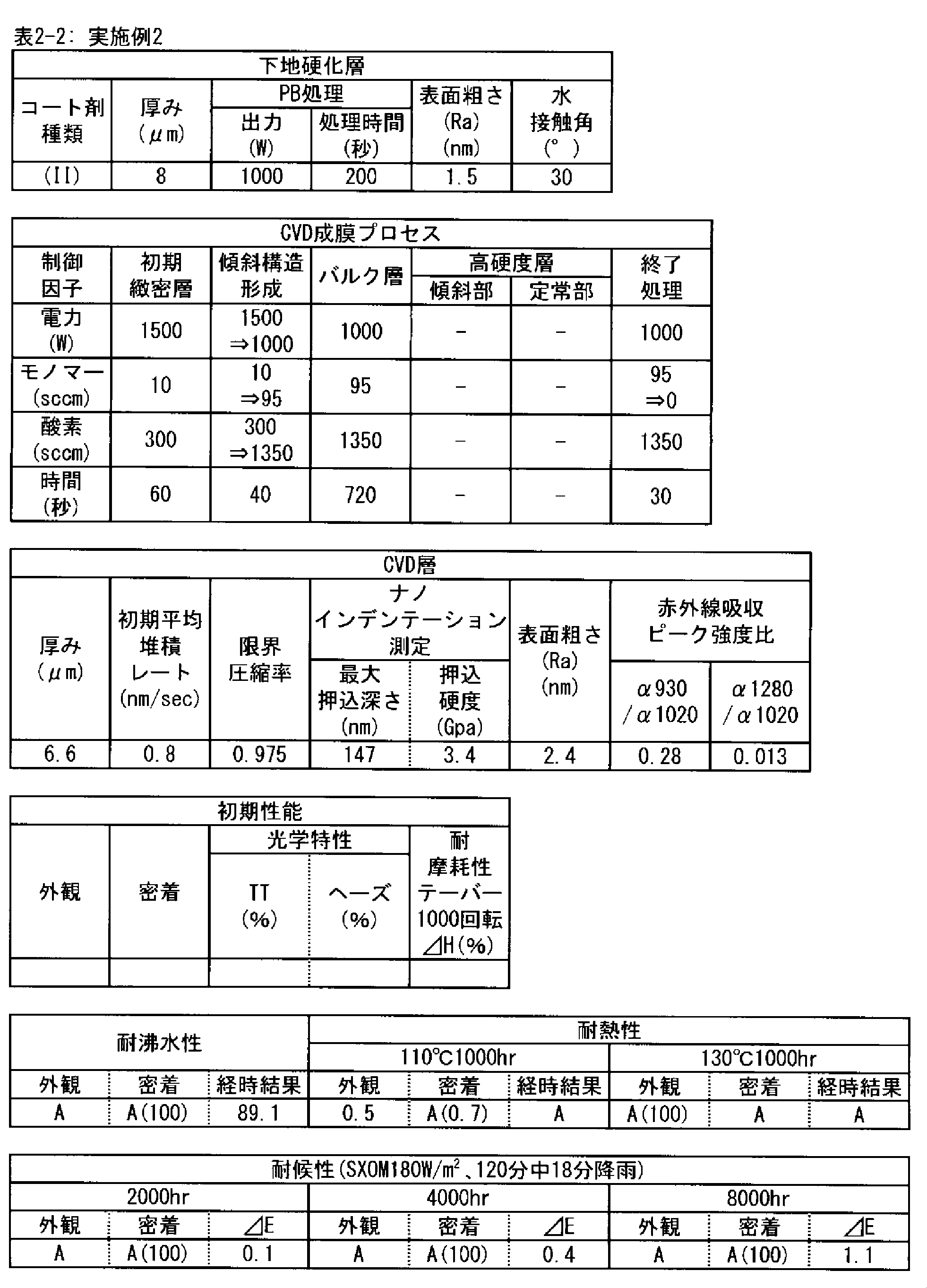


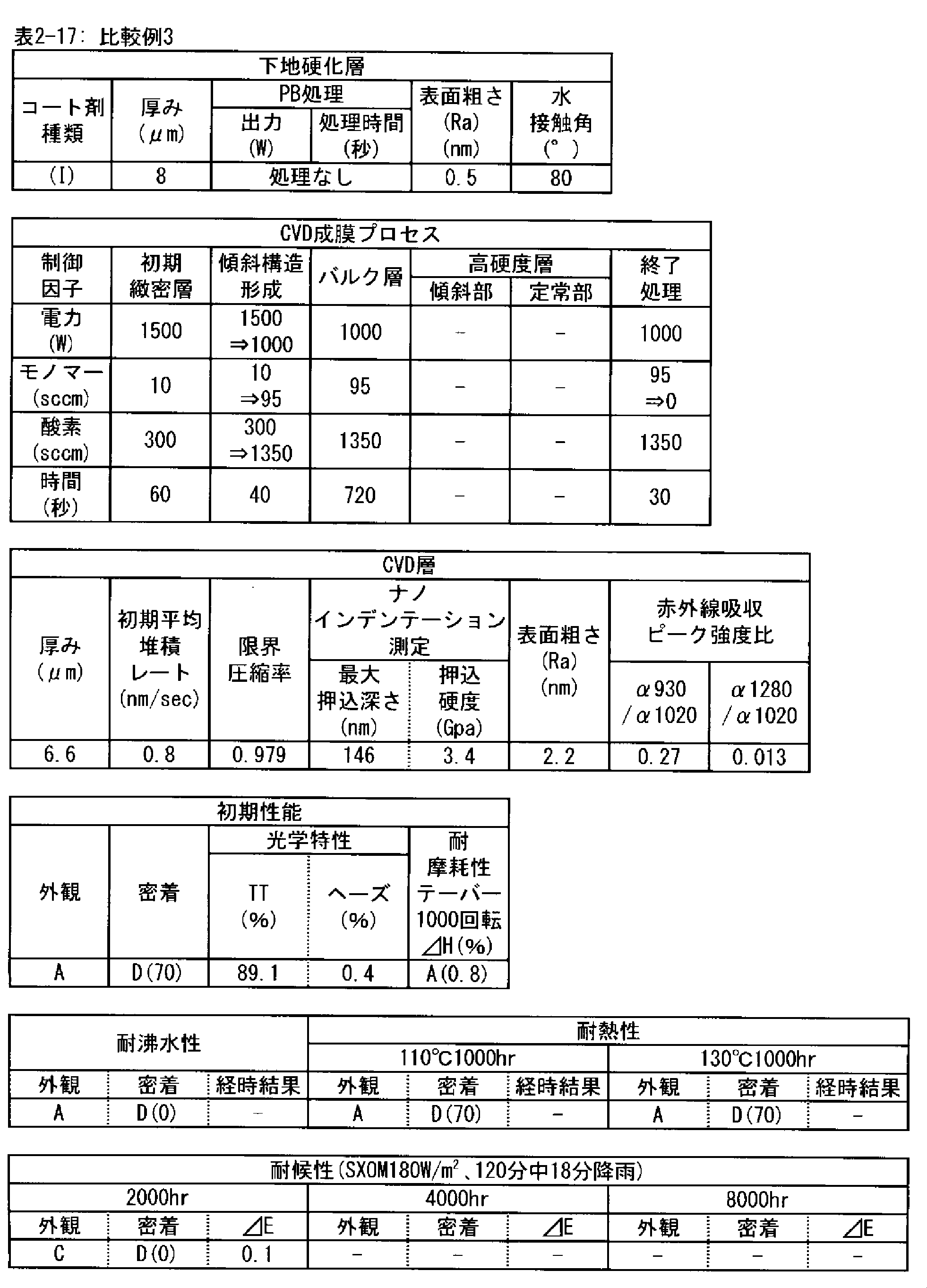


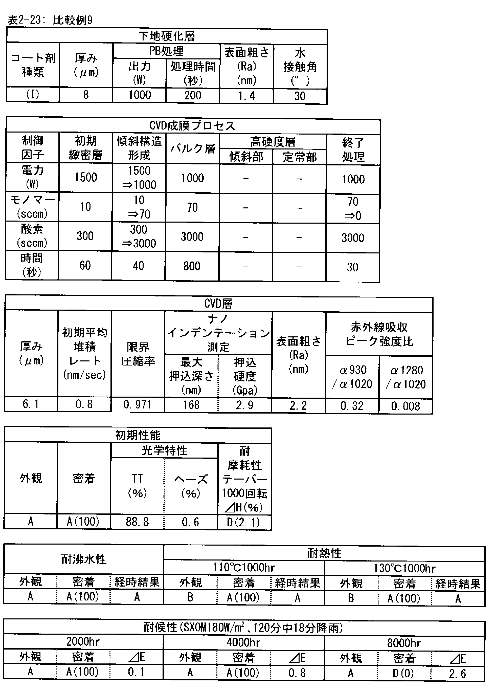


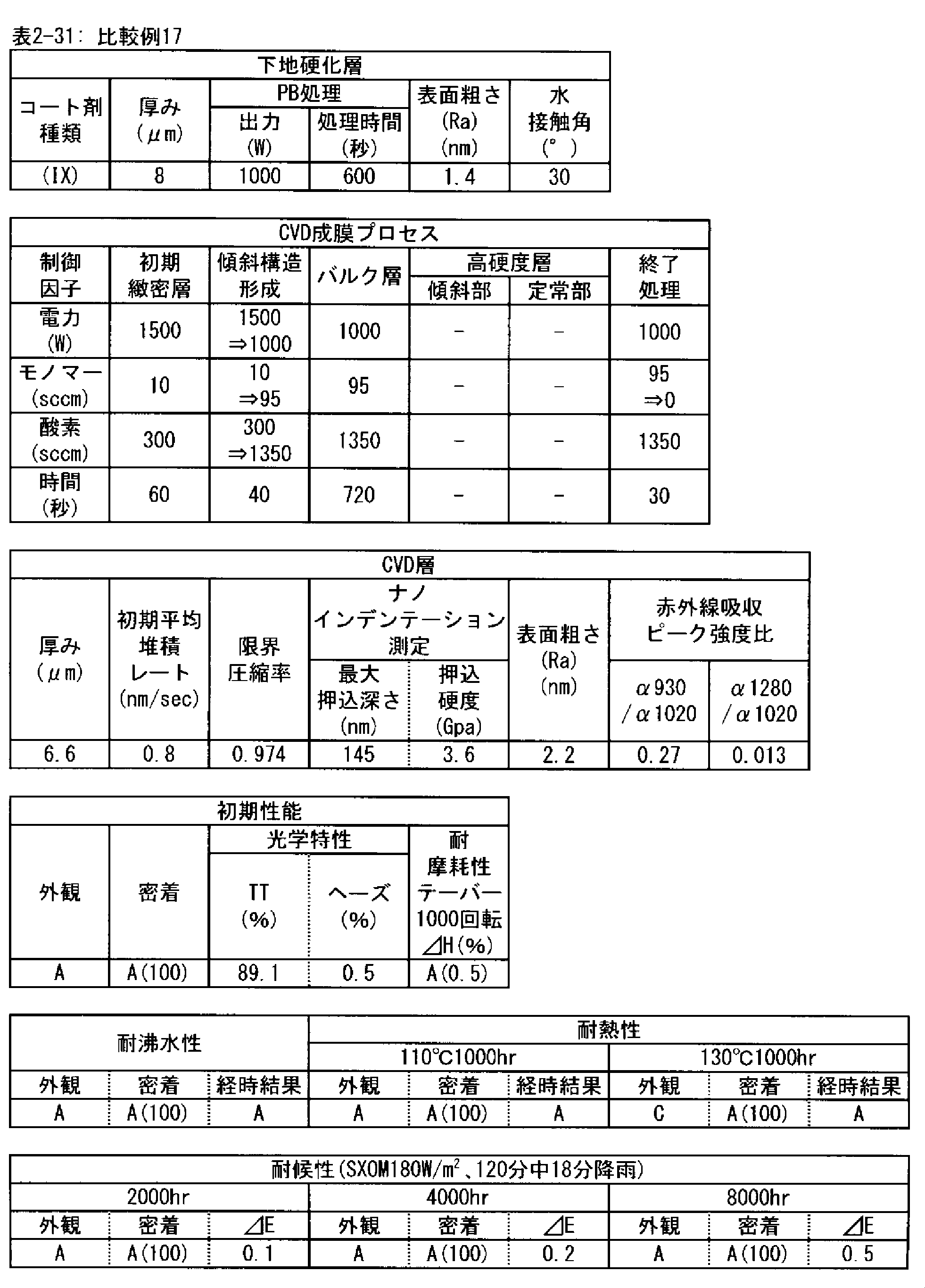
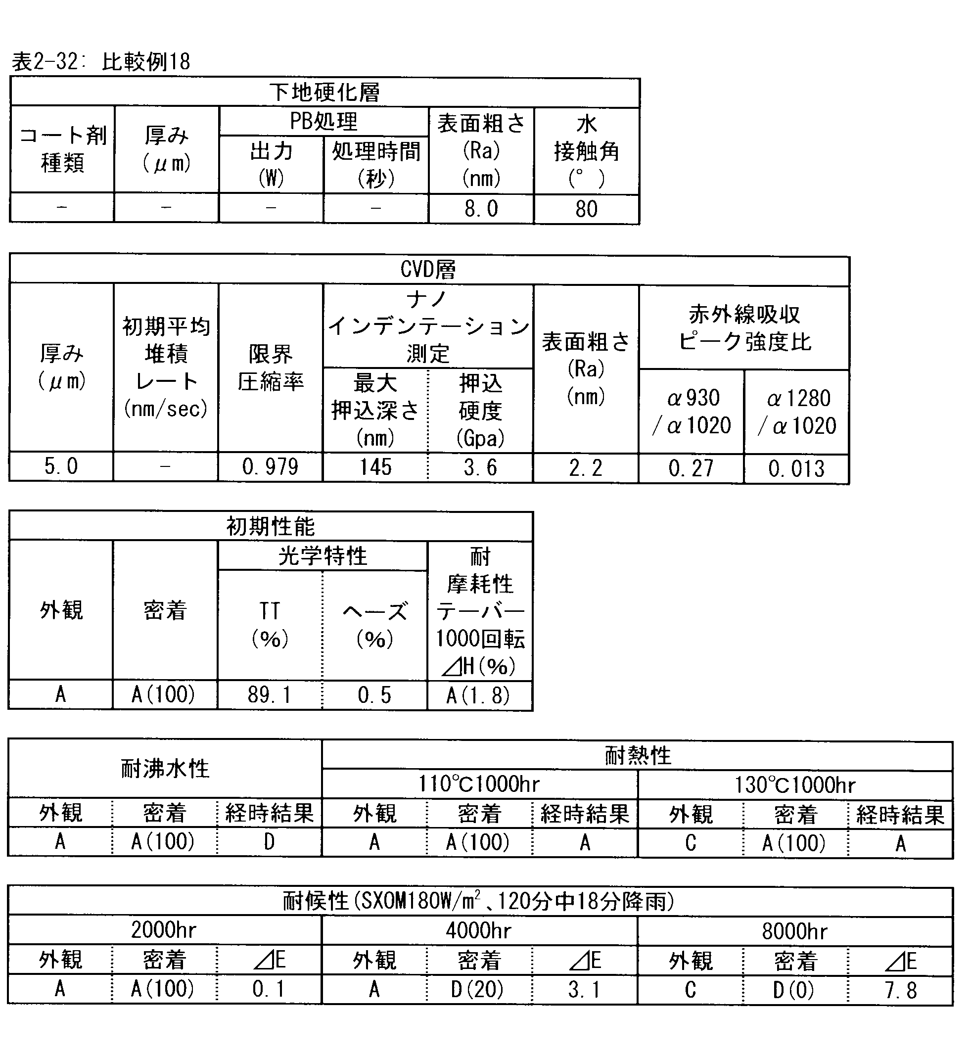


上記の表2-1~31からは、下地硬化層の厚さが1~20μmであり、酸化珪素層の膜厚が3.5~9.0μmの範囲であり、酸化珪素層のナノインデンテーション最大押し込み深さが150nm以下であり、かつ3点曲げ試験における酸化珪素層の限界圧縮率Kが0.975以下のときに、好ましい結果が得られることが理解される。これに対して、これらのいずれかを満たさない場合には、好ましい結果は得られなかった。具体的には、表2-1~31からは下記の点が理解された。
実施例1~4はPE-CVD法による酸化珪素層の形成条件は同一であり、必須の構成要件を満たしている。また、下地硬化層の組成、PE-CVD法による酸化珪素層の限界圧縮率には幾分の相違を生じているが、これらの各値ともに本願好適範囲内にある為、テーバー摩耗性、沸水性能、耐水性能、耐熱性能とも良好な結果が得られている。また促進耐候性についても良好結果であり、特に実施例1,2は、下地硬化層に無機紫外線吸収剤としてヒドロキシフェニルトリアジン系のチヌビン400が添加されている事に拠り、高分子基板および接着層の紫外線劣化を主要因とするハードコート層付高分子基板の色差(△E)が実施例3、4よりも相対的に抑制されている。
実施例5は、必須の構成要件を満たしており、さらに、下地硬化層のプラズマ処理時間が相対的に長い以外は実施例4と同様に作成しているが、下地硬化層のDFM法による表面粗さに相違があり、PE-CVD法による酸化珪素層の限界圧縮率にも幾分の相違を生じている。しかしながら、これらの各値ともに本願好適範囲内にある為、テーバー摩耗性、沸水性能、耐水性能、耐熱性能とも良好な結果が得られ、促進耐候性についても良好な結果が得られている。
実施例6は、必須の構成要件を満たし、PE-CVD法による酸化珪素層の膜厚が本願好適範囲の上限近くにあるが、下地硬化層およびPE-CVD法による酸化珪素層に関する本願好適範囲のパラメータを満足する為、テーバー摩耗性、沸水性能、耐水性能、耐熱性能とも良好な結果が得られ、促進耐候性についても良好な結果が得られている。
実施例11は、必須の構成要件を満たし、PE-CVD法による酸化珪素層の膜厚が本願好適範囲の下限近くにあるが、下地硬化層およびPE-CVD法による酸化珪素層に関する本願好適範囲のパラメータを満足する為、テーバー摩耗性、沸水性能、耐水性能、耐熱性能とも良好な結果が得られ、促進耐候性についても良好な結果が得られている。
実施例7~10は、必須の構成要件を満たしており、さらに、下地硬化層の組成、プラズマ処理条件が本願好適範囲内の同一条件であるが、PE-CVD法による酸化珪素層の作成条件(成膜条件)が相違しており、限界圧縮率、ナノインデンテーション最大押し込み深さ、押し込み硬度、DFM法による表面粗さも相違している。しかしながら、これらの各値ともに本願好適範囲内にある為、テーバー摩耗性、沸水性能、耐水性能、耐熱性能とも良好な結果が得られ、促進耐候性についても良好な結果が得られている。
実施例12は、必須の構成要件を満たし、下地硬化層の無機成分比率が本願好適範囲の下限近くにあるが、下地硬化層およびPE-CVD法による酸化珪素層に関する本願好適範囲のパラメータを満足する為、テーバー摩耗性、沸水性能、耐水性能、耐熱性能とも良好な結果が得られ、促進耐候性についても良好な結果が得られている。
実施例13は、必須の構成要件を満たし、下地硬化層組成に多官能(メタ)アクリレートと無機微粒子の分散性を向上するための有機-無機ハイブリッド型アクリル樹脂が含まれていないが、下地硬化層およびPE-CVD法による酸化珪素層に関する本願好適範囲のパラメータを満足する為、テーバー摩耗性、沸水性能、耐水性能、耐熱性能とも良好な結果が得られ、促進耐候性についても良好な結果が得られている。
実施例1~4、12,13と比較例1は、下地硬化層のプラズマ処理条件、PE-CVD法による酸化珪素層の形成条件で同一であるにも関わらず実施例1~4は良好結果、比較例1は評価に値する基板を得ることができなかった。比較例1は下地硬化層コート剤の無機成分比率が本願好適範囲を下回っており、必須の構成要件を満たしていない。この結果プラズマ処理により下地硬化層が分解・劣化して表面粗さが急上昇し、評価に値する酸化珪素層を形成できなくなった。
実施例1~4、12,13と比較例2は、下地硬化層のプラズマ処理条件、PE-CVD法による酸化珪素層の形成条件で同一であるにも関わらず、沸水性能、耐水性能、促進耐候性能が相違しており、実施例1~4は良好結果、比較例2は不十分な結果であった。ここで実施例1~4,12,13は限界圧縮率が本願好適範囲内にあったが、比較例2は外れており、必須の構成要件を満たしていない。また実施例1~4,12,13は下地硬化層が好適組成であったが、それに対して、比較例2は無機成分の比率が好適範囲の上限を上回っていた。
実施例1と比較例15は、下地硬化層が同一で、プラズマ処理条件、PE-CVD法による酸化珪素層の形成条件が同一であるにも関わらず、沸水性能、耐水性能、促進耐候性能が相違しており、実施例1は良好結果、比較例15は不十分な結果であった。ここで実施例1は限界圧縮率が本願好適範囲内にあったが、比較例15は外れており、必須の構成要件を満たしていない。また実施例1はPE-CVD法による酸化珪素層の初期堆積レートが本願好適範囲内にあったが、それに対して、さらに比較例15は外れていた。
実施例1と比較例3、4とは、下地硬化層の組成、PE-CVD法による酸化珪素層の形成条件が同一であるにも関わらず、沸水性能、促進耐候性能が相違しており、実施例1は良好結果、比較例3、4は不十分な結果であった。ここで実施例1は限界圧縮率が本願好適範囲内にあったが、比較例3、4は外れており、必須の構成要件を満たしていない。また実施例1は下地硬化層のDFM法による表面粗さ、水接触角が本願好適範囲内にあったが、それに対して、さらに比較例3、4は外れていた。これらの相違は下地硬化層のプラズマ処理条件の相違に拠るものである。
実施例6と比較例5~8および12とは、下地硬化層の組成、プラズマ処理条件、下地硬化層のDFM法による表面粗さ、水接触角が同一であるにも関わらず、沸水性能、促進耐候性能が相違しており、実施例4は良好結果、比較例5~8および12は不十分な結果であった。ここで実施例1および6~11は限界圧縮率が本願好適範囲内にあったが、比較例5~8および12は外れており、必須の構成要件を満たしていない。
実施例1および6~11と比較例9~11および16は、下地硬化層組成、プラズマ処理条件、下地硬化層のDFM法による表面粗さ、および水接触角が同一であるにも関わらず、耐摩耗性能が相違しており、実施例1および6~11は良好結果、比較例9~11および16は不十分な結果であった。ここで実施例1および6~11はナノインデンテーション測定による最大押込深さが本願好適範囲内にあったが、比較例9~11は外れており、必須の構成要件を満たしていない。また実施例1および6~11はPE-CVD法による酸化珪素層の赤外吸収ピーク強度比(α1280/α1020)(α930/α1020)が本願好適範囲内にあったが、それに対して、さらに比較例9~11および16は外れていた。これら相違はPE-CVD法による酸化珪素層の成膜条件の相違に拠るものである。
比較例13は実施例8と類似条件で作成されたものであるが、実施例8と異なり、テーバー摩耗性が不十分な結果であった。これは比較例13のPE-CVD法による酸化珪素層の膜厚は本願好適範囲を下回っており、必須の構成要件を満たしていない事に拠る。
比較例14は実施例8と類似条件で作成されたものであるが、実施例8と異なり、沸水性能、促進耐候性能が不十分な結果であった。これは比較例14のPE-CVD法による酸化珪素層の膜厚が本願好適範囲を上回っており、必須の構成要件を満たしていない事による。
実施例11と比較例16はPE-CVD法による酸化珪素層の膜厚がほぼ同等であるが、テーバー摩耗性について実施例11は良好、比較例16は不十分な結果であった。この相違は、PE-CVD法による酸化珪素層のナノインデンテーション最大押し込み深さ、押し込み硬度に関し、実施例11は本願好適範囲内にあり、比較例16は、外れており、必須の構成要件を満たしていない事に拠る。
実施例1と比較例17は、PE-CVD法による酸化珪素層の形成条件が同一で、プラズマ処理後の下地硬化層表面の表面粗さ・水接触角が共に本願好適範囲内であるだけでなく限界圧縮率についても両者共に本願好適範囲内であるにも関わらず、実施例1は130℃1000時間の耐熱性が良好であるのに対し、比較例17では同試験でコート層にクラックが入った。これは下地硬化層が本願好適範囲の紫外線硬化型アクリル樹脂層であるのに対し、比較例17では(線膨張率差の影響での引っ張り応力に対する耐久性の意味で)耐熱性が劣る熱硬化型シロキサン樹脂層となっていることが原因である。
実施例1と比較例18および20は、両者共に初期性能は良好であったが、比較例18および20については、耐沸水試験後の経過観察でクラックが生じ、かつ部分的に剥離が生じた。また、130℃1000時間の耐熱性試験で、部分的な剥離が生じた。これは実施例1の限界圧縮率が本願好適範囲内であるが、比較例18および20は外れていることが原因である。
実施例1と比較例19は、両者共に初期性能は良好であったが、比較例19については、耐沸水試験後の経過観察でクラックが生じ、かつ部分的に剥離が生じた。また、130℃1000時間の耐熱性試験で、部分的な剥離が生じた。これは実施例1における酸化珪素層の膜厚が本願好適範囲内であるが、比較例19は外れていることが原因である。
2 電源
3 マッチングボックス
4 排気口
5 真空ポンプ
6A 冷却媒体
7 反応ガス
10 カソード電極
14 シールド部品
20 アノード電極
30、31 被処理基板
40、41 ガス導入ヘッド
40A、41A 吹き出し孔
40B、41B 流入孔
50 高分子基板
60 接着層
70 下地硬化層
80 PE-CVD法による酸化珪素層
81 切り込み線(剥離開始線)
90 3点曲げ試験装置(押し込み荷重印加側)
90A、90B 端部支点
100 3点曲げ試験装置(支点側)
100A 中心支点
110 押し込み荷重の印加方向
120 切り込み加工用刃物
130 曲率中心
Claims (11)
- 厚み1~20mmの高分子基板、およびその表面上のハードコート層を具備しているハードコート層付高分子基板であって、
上記ハードコート層が、
上記高分子基板の表面上に積層されており、多官能アクリレート10~90重量部、無機酸化物微粒子および/または珪素化合物加水分解縮合物90~10重量部を含み、かつ厚みが1~20μmである、下地硬化層と、
上記高分子基板と反対側で上記下地硬化層に直接に接しており、有機珪素化合物を原料として用いたPE-CVD法によって形成され、かつ下記(a)~(c)のすべての要件を満たす、酸化珪素層と
を具備してなる、ハードコート層付高分子基板:
(a)上記酸化珪素層の膜厚が3.5~9.0μmの範囲にあること、
(b)最大荷重1mN条件でのナノインデンテーション測定による上記酸化珪素層の表面の最大押し込み深さが、150nm以下であること、
(c)上記酸化珪素層が積層されている面が凹となる押し込み変位を与える上記ハードコート層付高分子基板の3点曲げ試験において、下記式(1)で定義される上記酸化珪素層の限界圧縮率Kの値が0.975以下であること:
K=(R-D/2)/R-(0.00215×d) …式(1)
(ここで、
Dは、ハードコート層付高分子基板の全体厚み(mm)、
dは、酸化珪素層の膜厚(μm)、
Gは、3点曲げ試験装置における端部2支点間距離(mm)、
δLは、3点曲げ試験中に加重印加の中心支点位置に予め引いた切り込み線(剥離開始線)から上記酸化珪素層が剥離を開始する時の、押し込み変位量(mm)
Rは、3点曲げ試験中に加重印加の中心支点位置に予め引いた切り込み線(剥離開始線)から上記酸化珪素層が剥離を開始する時の、上記ハードコート層付高分子基板の曲率半径(mm))。 - 上記酸化珪素層の波数930cm-1と1020cm-1の赤外線吸光度の比(α930/α1020)が、0.30以下である、請求項1に記載のハードコート層付高分子基板。
- 上記酸化珪素層の波数1280cm-1と1020cm-1の赤外線吸光度の比(α1280/α1020)が、0.002~0.020の範囲にある、請求項1または2に記載のハードコート層付高分子基板。
- 最大荷重1mN条件でのナノインデンテーション測定において、上記酸化珪素層の表面の押し込み硬度が3.0GPa以上である、請求項1~3のいずれか一項に記載のハードコート層付高分子基板。
- 走査型プローブ顕微鏡のダイナミックフォースモード(DFM)を用いて5μm四方の観察条件で測定したときに、上記酸化珪素層の表面粗さ(Ra)が5.0nm以下である、請求項1~4のいずれか一項に記載のハードコート層付高分子基板。
- 上記下地硬化層に、水酸基、アミノ基、カルボキシル基もしくはアルコキシシリル基、またはそれらの組合せを化合物中に0.1~5mol/kg含む(メタ)アクリル樹脂を含有する、請求項1~5のいずれか一項に記載のハードコート層付高分子基板。
- 多官能アクリレート10~90重量部、無機酸化物微粒子および/または珪素化合物加水分解縮合物90~10重量部を含む前駆材料組成物を、上記高分子基板に塗布、乾燥、熱硬化又は活性エネルギー線硬化することにより、上記下地硬化層を形成することを含む、請求項1~6のいずれか一項に記載のハードコート層付高分子基板の製造方法。
- 上記下地硬化層の表面を、プラズマ励起もしくはイオン化された不活性ガスを上記下地硬化層の表面に衝突させる事により調整する、請求項7に記載のハードコート層付高分子基板の製造方法。
- 上記酸化珪素層を、堆積開始から開始30秒後までの平均堆積レート(nm/sec)を1nm/sec以下として形成する、請求項7または8に記載のハードコート層付高分子基板の製造方法。
- 上記酸化珪素層を、堆積開始から開始30秒後以降の平均堆積レート(nm/sec)を2nm/sec以上として形成する、請求項9に記載のハードコート層付高分子基板の製造方法。
- 上記酸化珪素層の堆積のレートを、2又はそれよりも多くの段階に分けて段階的に、又は連続的に、増加させる、請求項10に記載のハードコート層付高分子基板の製造方法。
Priority Applications (8)
| Application Number | Priority Date | Filing Date | Title |
|---|---|---|---|
| MX2018003451A MX2018003451A (es) | 2015-09-25 | 2016-09-23 | Sustrato polimerico con capa de cubierta dura y metodo de manufacturacion para el mismo. |
| BR112018005528-0A BR112018005528A2 (ja) | 2015-09-25 | 2016-09-23 | A polymers board with a hard court layer, and a manufacturing method for the same |
| AU2016328952A AU2016328952B2 (en) | 2015-09-25 | 2016-09-23 | Polymer substrate with hardcoat layer, and manufacturing method for same |
| JP2017540939A JP6715849B2 (ja) | 2015-09-25 | 2016-09-23 | ハードコート層付高分子基板およびその製造方法 |
| EP16848702.3A EP3354455B1 (en) | 2015-09-25 | 2016-09-23 | Polymer substrate with hardcoat layer, and manufacturing method for same |
| CN201680055280.3A CN108093628B (zh) | 2015-09-25 | 2016-09-23 | 带有硬涂层的高分子基板及其制造方法 |
| US15/761,348 US11028284B2 (en) | 2015-09-25 | 2016-09-23 | Polymer substrate with hardcoat layer, and manufacturing method for same |
| KR1020187011513A KR20180056753A (ko) | 2015-09-25 | 2016-09-23 | 하드 코트층이 부착된 고분자 기판 및 그 제조 방법 |
Applications Claiming Priority (2)
| Application Number | Priority Date | Filing Date | Title |
|---|---|---|---|
| JP2015189003 | 2015-09-25 | ||
| JP2015-189003 | 2015-09-25 |
Publications (1)
| Publication Number | Publication Date |
|---|---|
| WO2017051914A1 true WO2017051914A1 (ja) | 2017-03-30 |
Family
ID=58386083
Family Applications (1)
| Application Number | Title | Priority Date | Filing Date |
|---|---|---|---|
| PCT/JP2016/078127 Ceased WO2017051914A1 (ja) | 2015-09-25 | 2016-09-23 | ハードコート層付高分子基板およびその製造方法 |
Country Status (9)
| Country | Link |
|---|---|
| US (1) | US11028284B2 (ja) |
| EP (1) | EP3354455B1 (ja) |
| JP (1) | JP6715849B2 (ja) |
| KR (1) | KR20180056753A (ja) |
| CN (1) | CN108093628B (ja) |
| AU (1) | AU2016328952B2 (ja) |
| BR (1) | BR112018005528A2 (ja) |
| MX (1) | MX2018003451A (ja) |
| WO (1) | WO2017051914A1 (ja) |
Cited By (9)
| Publication number | Priority date | Publication date | Assignee | Title |
|---|---|---|---|---|
| WO2018181572A1 (ja) * | 2017-03-29 | 2018-10-04 | 帝人株式会社 | ハードコート層付高分子基板 |
| CN108976452A (zh) * | 2017-06-05 | 2018-12-11 | 日本化工涂料株式会社 | 在环状烯烃系树脂基材上形成固化覆膜的活性能量射线固化型组合物及所得硬涂膜和层叠体 |
| JP2019105830A (ja) * | 2017-12-08 | 2019-06-27 | 住友化学株式会社 | 光学積層体 |
| JP2019105829A (ja) * | 2017-12-08 | 2019-06-27 | 住友化学株式会社 | 光学積層体 |
| JP2020007382A (ja) * | 2018-07-02 | 2020-01-16 | キヤノン株式会社 | コーティング組成物とその製造方法、および光学部材、ならびに撮像装置 |
| KR20210014748A (ko) * | 2018-08-14 | 2021-02-09 | 어플라이드 머티어리얼스, 인코포레이티드 | 가요성 커버 렌즈용 다층 습식-건식 하드코트들 |
| JP2021169210A (ja) * | 2020-04-13 | 2021-10-28 | ダイキョーニシカワ株式会社 | 積層体及びその製造方法 |
| CN113663840A (zh) * | 2021-08-26 | 2021-11-19 | 合肥聚能电物理高技术开发有限公司 | 一种外氮屏铜喷涂工装及其喷涂工艺 |
| WO2025033174A1 (ja) * | 2023-08-04 | 2025-02-13 | 古河電気工業株式会社 | コート層付金属箔及び金属張積層板 |
Families Citing this family (15)
| Publication number | Priority date | Publication date | Assignee | Title |
|---|---|---|---|---|
| KR101943750B1 (ko) * | 2017-09-14 | 2019-01-30 | 매그나칩 반도체 유한회사 | 플렉서블 반도체 칩 패키지의 벤딩 테스트 소켓 및 이를 이용한 벤딩 테스트 방법 |
| CN111278643A (zh) | 2017-10-27 | 2020-06-12 | 应用材料公司 | 柔性盖板透镜膜 |
| KR102691346B1 (ko) | 2018-05-10 | 2024-08-05 | 어플라이드 머티어리얼스, 인코포레이티드 | 플렉서블 디스플레이를 위한 교체가능한 커버 렌즈 |
| US11851325B2 (en) * | 2018-11-30 | 2023-12-26 | Taiwan Semiconductor Manufacturing Co., Ltd. | Methods for wafer bonding |
| CN113365825B (zh) * | 2018-12-06 | 2024-05-10 | 日涂汽车涂料有限公司 | 装饰用层合构件和装饰性成型品的制造方法 |
| KR20240144481A (ko) * | 2018-12-28 | 2024-10-02 | 다이니폰 인사츠 가부시키가이샤 | 광학 필름, 편광자 보호 필름, 편광자 보호 필름용 전사체, 편광판, 화상 표시 장치, 및 편광자 보호 필름의 제조 방법 |
| US11442201B2 (en) * | 2019-04-01 | 2022-09-13 | Microcosm Technology Co., Ltd. | Flexible display cover substrate |
| JP7598888B2 (ja) | 2019-06-26 | 2024-12-12 | アプライド マテリアルズ インコーポレイテッド | 折り畳み式ディスプレイ用の可撓性多層カバーレンズ積層体 |
| CN110387529B (zh) * | 2019-07-05 | 2021-08-10 | 中国人民解放军空军勤务学院 | 一种用于液压阀杆表面防护的复合涂层及其制备方法 |
| KR20210091385A (ko) * | 2020-01-13 | 2021-07-22 | 삼성디스플레이 주식회사 | 표시모듈 및 이의 제조 방법 |
| JP7747619B2 (ja) * | 2020-03-27 | 2025-10-01 | 株式会社ユポ・コーポレーション | 粘着シート積層体及びその製造方法 |
| CN112109429B (zh) * | 2020-09-08 | 2022-03-04 | 杭州大云自动化科技有限公司 | 一种烫片机 |
| CN113862616B (zh) * | 2021-09-30 | 2023-10-20 | 台州星星光电科技有限公司 | 一种增透抗uv车载显示面板的一次镀膜成型方法 |
| CN115709156B (zh) * | 2022-11-15 | 2023-06-30 | 中科伟通智能科技(江西)有限公司 | 一种贯穿式车灯用uv固化生产线 |
| CN115926395B (zh) * | 2022-12-28 | 2024-08-23 | 宁波惠之星新材料科技股份有限公司 | 一种光学膜及其制备方法 |
Citations (5)
| Publication number | Priority date | Publication date | Assignee | Title |
|---|---|---|---|---|
| JPS644343A (en) * | 1987-04-06 | 1989-01-09 | Gen Electric | Manufacture of abrasion-resistant polycarbonate article and manufactured article |
| JP2004237513A (ja) * | 2003-02-05 | 2004-08-26 | Teijin Chem Ltd | 高分子樹脂積層体、ならびに車両用窓材 |
| JP2010253683A (ja) * | 2009-04-21 | 2010-11-11 | Tsukishima Kikai Co Ltd | プラスチック積層体及びその製造方法 |
| JP2013035275A (ja) * | 2011-07-13 | 2013-02-21 | Kansai Paint Co Ltd | 積層体及び積層体の製造方法 |
| JP5944069B2 (ja) * | 2014-03-27 | 2016-07-05 | 帝人株式会社 | ハードコート層付高分子基板およびその製造方法 |
Family Cites Families (9)
| Publication number | Priority date | Publication date | Assignee | Title |
|---|---|---|---|---|
| US6376064B1 (en) | 1999-12-13 | 2002-04-23 | General Electric Company | Layered article with improved microcrack resistance and method of making |
| JP4429515B2 (ja) * | 2000-03-09 | 2010-03-10 | 帝人株式会社 | 高分子樹脂積層体、その製造方法、および該積層体からなる成形物 |
| EP2090594B1 (en) * | 2006-11-09 | 2010-11-24 | DIC Corporation | Active-energy-ray-curable water-based resin composition, active-energy-ray-curable coating material, method of forming cured coating film, and article |
| JP5076729B2 (ja) * | 2007-08-20 | 2012-11-21 | 凸版印刷株式会社 | 反射防止フィルム及びそれを用いた偏光板 |
| US8361607B2 (en) | 2011-04-14 | 2013-01-29 | Exatec Llc | Organic resin laminate |
| JP6057320B2 (ja) | 2011-07-13 | 2017-01-11 | 関西ペイント株式会社 | 積層体及び積層体の製造方法 |
| US9441133B2 (en) | 2011-08-26 | 2016-09-13 | Exatec, Llc | Organic resin laminate, methods of making and using the same, and articles comprising the same |
| JP5042392B1 (ja) | 2011-10-24 | 2012-10-03 | 尾池工業株式会社 | 高耐擦傷性ハードコートフィルム |
| US20170356841A1 (en) * | 2016-06-13 | 2017-12-14 | Viavi Solutions Inc. | Optical filter including a high refractive index material |
-
2016
- 2016-09-23 US US15/761,348 patent/US11028284B2/en active Active
- 2016-09-23 WO PCT/JP2016/078127 patent/WO2017051914A1/ja not_active Ceased
- 2016-09-23 AU AU2016328952A patent/AU2016328952B2/en not_active Ceased
- 2016-09-23 MX MX2018003451A patent/MX2018003451A/es unknown
- 2016-09-23 EP EP16848702.3A patent/EP3354455B1/en active Active
- 2016-09-23 JP JP2017540939A patent/JP6715849B2/ja active Active
- 2016-09-23 BR BR112018005528-0A patent/BR112018005528A2/ja not_active Application Discontinuation
- 2016-09-23 KR KR1020187011513A patent/KR20180056753A/ko not_active Withdrawn
- 2016-09-23 CN CN201680055280.3A patent/CN108093628B/zh active Active
Patent Citations (5)
| Publication number | Priority date | Publication date | Assignee | Title |
|---|---|---|---|---|
| JPS644343A (en) * | 1987-04-06 | 1989-01-09 | Gen Electric | Manufacture of abrasion-resistant polycarbonate article and manufactured article |
| JP2004237513A (ja) * | 2003-02-05 | 2004-08-26 | Teijin Chem Ltd | 高分子樹脂積層体、ならびに車両用窓材 |
| JP2010253683A (ja) * | 2009-04-21 | 2010-11-11 | Tsukishima Kikai Co Ltd | プラスチック積層体及びその製造方法 |
| JP2013035275A (ja) * | 2011-07-13 | 2013-02-21 | Kansai Paint Co Ltd | 積層体及び積層体の製造方法 |
| JP5944069B2 (ja) * | 2014-03-27 | 2016-07-05 | 帝人株式会社 | ハードコート層付高分子基板およびその製造方法 |
Non-Patent Citations (1)
| Title |
|---|
| See also references of EP3354455A4 * |
Cited By (19)
| Publication number | Priority date | Publication date | Assignee | Title |
|---|---|---|---|---|
| US11866564B2 (en) | 2017-03-29 | 2024-01-09 | Teijin Limited | Polymer substrate with hard coat layer |
| WO2018181572A1 (ja) * | 2017-03-29 | 2018-10-04 | 帝人株式会社 | ハードコート層付高分子基板 |
| CN108976452A (zh) * | 2017-06-05 | 2018-12-11 | 日本化工涂料株式会社 | 在环状烯烃系树脂基材上形成固化覆膜的活性能量射线固化型组合物及所得硬涂膜和层叠体 |
| TWI842673B (zh) * | 2017-06-05 | 2024-05-21 | 日商日本化工塗料股份有限公司 | 用以在環狀烯烴系樹脂基材上形成硬化被膜之活性能量線硬化型組成物、以及以環狀烯烴系樹脂為基材之硬塗薄膜及積層體 |
| CN108976452B (zh) * | 2017-06-05 | 2022-12-09 | 日本化工涂料株式会社 | 在环状烯烃系树脂基材上形成固化覆膜的活性能量射线固化型组合物及所得硬涂膜和层叠体 |
| JP2019105830A (ja) * | 2017-12-08 | 2019-06-27 | 住友化学株式会社 | 光学積層体 |
| JP2019105829A (ja) * | 2017-12-08 | 2019-06-27 | 住友化学株式会社 | 光学積層体 |
| JP7129247B2 (ja) | 2018-07-02 | 2022-09-01 | キヤノン株式会社 | コーティング組成物とその製造方法、および光学部材、ならびに撮像装置 |
| JP2020007382A (ja) * | 2018-07-02 | 2020-01-16 | キヤノン株式会社 | コーティング組成物とその製造方法、および光学部材、ならびに撮像装置 |
| JP2021536030A (ja) * | 2018-08-14 | 2021-12-23 | アプライド マテリアルズ インコーポレイテッドApplied Materials, Incorporated | フレキシブルカバーレンズのための多層乾湿ハードコート |
| US11988810B2 (en) | 2018-08-14 | 2024-05-21 | Applied Materials, Inc. | Multi-layer wet-dry hardcoats for flexible cover lens |
| KR20210014748A (ko) * | 2018-08-14 | 2021-02-09 | 어플라이드 머티어리얼스, 인코포레이티드 | 가요성 커버 렌즈용 다층 습식-건식 하드코트들 |
| KR102680576B1 (ko) * | 2018-08-14 | 2024-07-01 | 어플라이드 머티어리얼스, 인코포레이티드 | 가요성 커버 렌즈용 다층 습식-건식 하드코트들 |
| US20240288610A1 (en) * | 2018-08-14 | 2024-08-29 | Applied Materials, Inc. | Multi-layer wet-dry hardcoats for flexible cover lens |
| JP2021169210A (ja) * | 2020-04-13 | 2021-10-28 | ダイキョーニシカワ株式会社 | 積層体及びその製造方法 |
| JP7640345B2 (ja) | 2020-04-13 | 2025-03-05 | ダイキョーニシカワ株式会社 | 積層体及びその製造方法 |
| CN113663840A (zh) * | 2021-08-26 | 2021-11-19 | 合肥聚能电物理高技术开发有限公司 | 一种外氮屏铜喷涂工装及其喷涂工艺 |
| WO2025033174A1 (ja) * | 2023-08-04 | 2025-02-13 | 古河電気工業株式会社 | コート層付金属箔及び金属張積層板 |
| JP7654911B1 (ja) * | 2023-08-04 | 2025-04-01 | 古河電気工業株式会社 | コート層付金属箔及び金属張積層板 |
Also Published As
| Publication number | Publication date |
|---|---|
| EP3354455A4 (en) | 2018-10-24 |
| US20180265731A1 (en) | 2018-09-20 |
| US11028284B2 (en) | 2021-06-08 |
| AU2016328952A1 (en) | 2018-04-19 |
| AU2016328952B2 (en) | 2020-09-03 |
| EP3354455B1 (en) | 2022-02-09 |
| CN108093628B (zh) | 2020-09-22 |
| KR20180056753A (ko) | 2018-05-29 |
| BR112018005528A2 (ja) | 2018-12-04 |
| CN108093628A (zh) | 2018-05-29 |
| MX2018003451A (es) | 2018-08-15 |
| EP3354455A1 (en) | 2018-08-01 |
| JP6715849B2 (ja) | 2020-07-01 |
| JPWO2017051914A1 (ja) | 2018-08-30 |
Similar Documents
| Publication | Publication Date | Title |
|---|---|---|
| JP6715849B2 (ja) | ハードコート層付高分子基板およびその製造方法 | |
| JP5944069B2 (ja) | ハードコート層付高分子基板およびその製造方法 | |
| JP5965225B2 (ja) | 微小亀裂耐性の向上した積層品及びその製造方法 | |
| CN110461589B (zh) | 带有硬涂层的高分子基板 | |
| EP2364844B1 (en) | Polycarbonate resin laminates | |
| JP7159336B2 (ja) | ハードコート層付高分子基板 | |
| JP6524261B2 (ja) | 積層体の製造方法 | |
| JP4118711B2 (ja) | 高分子樹脂積層体、およびその製造方法、ならびに車両用窓材 | |
| CN115279587A (zh) | 层叠体及层叠体的制造方法 | |
| JP2014065281A (ja) | 積層体とその製造方法 |
Legal Events
| Date | Code | Title | Description |
|---|---|---|---|
| 121 | Ep: the epo has been informed by wipo that ep was designated in this application |
Ref document number: 16848702 Country of ref document: EP Kind code of ref document: A1 |
|
| ENP | Entry into the national phase |
Ref document number: 2017540939 Country of ref document: JP Kind code of ref document: A |
|
| WWE | Wipo information: entry into national phase |
Ref document number: 15761348 Country of ref document: US |
|
| WWE | Wipo information: entry into national phase |
Ref document number: MX/A/2018/003451 Country of ref document: MX |
|
| NENP | Non-entry into the national phase |
Ref country code: DE |
|
| REG | Reference to national code |
Ref country code: BR Ref legal event code: B01A Ref document number: 112018005528 Country of ref document: BR |
|
| ENP | Entry into the national phase |
Ref document number: 2016328952 Country of ref document: AU Date of ref document: 20160923 Kind code of ref document: A |
|
| ENP | Entry into the national phase |
Ref document number: 20187011513 Country of ref document: KR Kind code of ref document: A |
|
| REG | Reference to national code |
Ref country code: BR Ref legal event code: B01E Ref document number: 112018005528 Country of ref document: BR |
|
| ENP | Entry into the national phase |
Ref document number: 112018005528 Country of ref document: BR Kind code of ref document: A2 Effective date: 20180320 |