WO2017073410A1 - アンテナ装置 - Google Patents
アンテナ装置 Download PDFInfo
- Publication number
- WO2017073410A1 WO2017073410A1 PCT/JP2016/080867 JP2016080867W WO2017073410A1 WO 2017073410 A1 WO2017073410 A1 WO 2017073410A1 JP 2016080867 W JP2016080867 W JP 2016080867W WO 2017073410 A1 WO2017073410 A1 WO 2017073410A1
- Authority
- WO
- WIPO (PCT)
- Prior art keywords
- antenna
- antenna element
- wiring board
- antenna device
- grounding
- Prior art date
- Legal status (The legal status is an assumption and is not a legal conclusion. Google has not performed a legal analysis and makes no representation as to the accuracy of the status listed.)
- Ceased
Links
Images




Classifications
-
- H—ELECTRICITY
- H01—ELECTRIC ELEMENTS
- H01Q—ANTENNAS, i.e. RADIO AERIALS
- H01Q9/00—Electrically-short antennas having dimensions not more than twice the operating wavelength and consisting of conductive active radiating elements
- H01Q9/04—Resonant antennas
- H01Q9/0407—Substantially flat resonant element parallel to ground plane, e.g. patch antenna
- H01Q9/045—Substantially flat resonant element parallel to ground plane, e.g. patch antenna with particular feeding means
-
- H—ELECTRICITY
- H01—ELECTRIC ELEMENTS
- H01Q—ANTENNAS, i.e. RADIO AERIALS
- H01Q1/00—Details of, or arrangements associated with, antennas
- H01Q1/36—Structural form of radiating elements, e.g. cone, spiral, umbrella; Particular materials used therewith
-
- H—ELECTRICITY
- H01—ELECTRIC ELEMENTS
- H01Q—ANTENNAS, i.e. RADIO AERIALS
- H01Q1/00—Details of, or arrangements associated with, antennas
- H01Q1/36—Structural form of radiating elements, e.g. cone, spiral, umbrella; Particular materials used therewith
- H01Q1/38—Structural form of radiating elements, e.g. cone, spiral, umbrella; Particular materials used therewith formed by a conductive layer on an insulating support
-
- H—ELECTRICITY
- H01—ELECTRIC ELEMENTS
- H01Q—ANTENNAS, i.e. RADIO AERIALS
- H01Q13/00—Waveguide horns or mouths; Slot antennas; Leaky-waveguide antennas; Equivalent structures causing radiation along the transmission path of a guided wave
- H01Q13/10—Resonant slot antennas
- H01Q13/16—Folded slot antennas
-
- H—ELECTRICITY
- H01—ELECTRIC ELEMENTS
- H01Q—ANTENNAS, i.e. RADIO AERIALS
- H01Q9/00—Electrically-short antennas having dimensions not more than twice the operating wavelength and consisting of conductive active radiating elements
- H01Q9/04—Resonant antennas
- H01Q9/0407—Substantially flat resonant element parallel to ground plane, e.g. patch antenna
- H01Q9/0421—Substantially flat resonant element parallel to ground plane, e.g. patch antenna with a shorting wall or a shorting pin at one end of the element
-
- H—ELECTRICITY
- H01—ELECTRIC ELEMENTS
- H01Q—ANTENNAS, i.e. RADIO AERIALS
- H01Q1/00—Details of, or arrangements associated with, antennas
- H01Q1/27—Adaptation for use in or on movable bodies
- H01Q1/32—Adaptation for use in or on road or rail vehicles
- H01Q1/325—Adaptation for use in or on road or rail vehicles characterised by the location of the antenna on the vehicle
- H01Q1/3275—Adaptation for use in or on road or rail vehicles characterised by the location of the antenna on the vehicle mounted on a horizontal surface of the vehicle, e.g. on roof, hood, trunk
Definitions
- the present invention relates to an antenna device.
- Monopole or dipole antennas usually require an antenna height of about ⁇ / 4 to ⁇ / 2, which increases the height of the outer case. For example, in the case of a 5.9 GHz band antenna, the height is about 12 mm.
- the element because of its shape, the element is difficult to stand on its own and the shape is not stable, and in most cases, an antenna holding member is required.
- Patent Document 1 discloses a thin antenna device that operates as a vertically polarized antenna that is omnidirectional with respect to an azimuth angle. Specifically, an opening with left and right partitions formed by connecting conductors is formed between the opposing peripheral edges of a pair of flat conductors, and the electric field distribution in the opening is similar to that of a slot antenna during power feeding. The vertical polarization is radiated in front of the opening.
- the antenna device is required to be further downsized.
- the current on the top surface is canceled in a complicated manner. Since the operation is similar to that of the slot antenna, sufficient radio wave reception cannot be ensured unless the size of at least about 20 ⁇ 20 ⁇ 4 mm (1600 mm 2 ) is secured, and the size cannot be sufficiently reduced.
- the present invention has been made in view of such circumstances, and an object thereof is to provide a further miniaturized antenna device for a non-directional vertically polarized antenna.
- An antenna device is provided with a flat antenna element disposed opposite to a grounded wiring board at an interval, and an end of the antenna element.
- a plurality of grounding legs to be connected; and an end of the antenna element; and a power feeding leg connected to a transmitting circuit or a receiving circuit, and the plurality of grounding legs are disposed.
- the surfaces formed by the respective end portions and the end portions on which the power supply leg portions are arranged are point-symmetric.
- a surface of the antenna element facing the wiring board is a regular polygon, and an end portion on which the feeding leg is disposed is one of the vertices of the regular polygon, The end where the grounding leg is arranged is the other apex of the regular polygon.
- each of the outer side portions connecting between the end portions where any two adjacent ones of the plurality of grounding leg portions and the feeding leg portions are arranged among the antenna elements is at least partially.
- the plurality of grounding leg portions and the power feeding leg portions are connected from the extension destinations of the portions not cut out of each of the outer side portions.
- the cutout portion is further provided, so that the current that should flow around the outer side portion meanders by the cutout portion, and as a result, a current path is further secured. Therefore, further downsizing can be realized.
- the plurality of grounding legs and the power feeding legs are formed in a planar shape extending from a portion not cut out of each of the outer side portions.
- the surface of the antenna element facing the wiring board is a regular triangle or a regular square.
- the surface of the antenna element facing the wiring board is a regular triangle or a regular square before being cut out.
- the wiring board is further provided, and the wiring board has a flat plate shape.
- a non-directional vertically polarized antenna can be realized by a combination of the antenna element and the wiring board.
- FIG. 1 is a diagram for explaining an antenna device having a triangular shape when viewed from the top surface according to an embodiment of the present invention.
- the antenna device having a triangular shape shown in FIG. 1 includes a flat plate-like grounded wiring board 100, a flat plate antenna element 110 that is disposed to face the wiring board 100 at an interval, and an end of the antenna element 110.
- the two extension legs 120 are arranged at the ends of the antenna element 110 and the extension destinations are connected to the circuit 150 (transmission circuit or reception circuit).
- the power supply leg 130 is provided.
- the antenna element 110 has a shape on a flat plate so as to be flat when viewed from the top surface (upper surface) and the back surface (lower surface).
- the figures forming the upper surface and the lower surface have the same shape, and have a certain thickness between the upper surface and the lower surface.
- the upper and lower surfaces of the antenna element 110 are point-symmetrical figures centered on the center point 111 and are regular polygons. In the example of FIG. 1, the upper surface and the lower surface of the antenna element 110 will be described as equilateral triangles.
- the antenna element 110 Since the upper surface of the antenna element 110 is an equilateral triangle, it has three vertices. In the example of FIG. 1, these three vertices will be described as end portions. The figure formed by connecting these three vertices and ends is a point-symmetric figure and is a regular polygon. In the example of FIG. 1, it is an equilateral triangle like the figure on the upper surface of the antenna element 110.
- the two grounding legs 120 are arranged at two ends of the antenna element 110 and two of the three vertices of the antenna element 110. Each of the two grounding legs 120 extends in the vertical and normal directions from the upper surface and the lower surface of the antenna element 110, and each extension destination is connected to the wiring substrate 100. Each of the two grounding legs 120 reaches the wiring substrate 100 from the vertical and normal directions, and each extension destination is connected to the wiring substrate 100.
- the power feeding leg portion 130 is disposed at one of the end portions of the antenna element 110 and the remaining one of the three vertices of the antenna element 110.
- the feeding legs 130 extend from the upper surface and the lower surface of the antenna element 110 in the vertical and normal directions, respectively, and the respective extending destinations are perpendicular to the wiring board 100 and extend from the normal direction.
- a hole 140 is formed in a direction toward the power feeding leg 130, and the power feeding leg 130 passes through the surface of the wiring board 100 so as not to contact the grounding part of the wiring board 100. .
- the power feeding leg 130 is finally connected to the circuit 150 (transmission circuit or reception circuit).
- the plane formed by the respective end portions where the plurality of grounding leg portions 120 are disposed and the end portions where the power feeding leg portions 130 are disposed is point-symmetric. Electric power is supplied from the circuit 150 to the antenna device via a power supply line.
- a deformed loop antenna having openings of about ⁇ / 2 in four directions is formed by the antenna element 110, and can stand by itself in a low posture and is vertically omnidirectional radiation characteristics.
- An antenna device having The basic operation is a loop antenna of about 1 ⁇ , and the top surface shape of the antenna element 110 and the two grounding leg portions 120 connected to the wiring substrate 100 as GND and the power feeding leg portion 130 are configured as point targets.
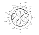
- FIG. 2 is a diagram for explaining the radiation characteristics of the antenna device having a triangular shape when viewed from the top surface according to the embodiment of the present invention.
- a waveform 170 indicates vertical polarization
- a waveform 180 indicates horizontal polarization.
- the volume constituting the antenna element is such that one side of the equilateral triangle forming the antenna element 110 is 17.3 mm, and the height of each leg is 4.5 mm. it can.
- the antenna device can be downsized compared to the antenna device that has to have a side of about 20 mm, and downsizing of about 38% can be realized.
- FIG. 3 is a diagram for explaining an antenna device having a square shape when viewed from the top surface according to the embodiment of the present invention.
- FIG. 3 is a diagram in which the shape of the upper surface and the lower surface of the antenna device shown in FIG.
- the square antenna device shown in FIG. 3 includes a flat plate-like grounded wiring board 200, a flat plate-like antenna element 210 disposed opposite to the wiring board 200 at an interval, and an end of the antenna element 210.
- Three grounding legs 220 each extending to be connected to the wiring board 200, and a power feeding leg 230 that is arranged at the end of the antenna element 210 and whose extending destination is connected to the circuit 250. Is provided.
- the upper surface of the antenna element 210 is square, it has four vertices. In the example of FIG. 3, these four vertices will be described as end portions. In the example of FIG. 3, the figure formed by connecting these four vertices and ends is a square like the figure on the upper surface of the antenna element 210.
- the three grounding legs 220 are arranged at two ends of the antenna element 210 and three of the four vertices of the antenna element 210. Each of the three grounding legs 220 extends in the vertical and normal directions from the upper surface and the lower surface of the antenna element 210, and each extension destination is connected to the wiring board 200. Each of the two grounding legs 220 also reaches the wiring board 200 from the vertical and normal directions, and each extension destination is connected to the wiring board 200.
- the power feeding leg 230 is arranged at one of the end portions of the antenna element 210 and the remaining one of the four vertices of the antenna element 210.
- the feeding legs 230 extend vertically and in the normal direction from the upper surface and the lower surface of the antenna element 210, respectively, and each extending destination is perpendicular to the wiring board 200 and extends from the normal direction.
- a hole 240 is formed at a destination of the power feeding leg 230, and the power feeding leg 230 passes through the surface of the wiring board 200 so as not to contact the grounding part of the wiring board 200.
- the power feeding leg 230 is finally connected to a circuit 250 (transmission circuit or reception circuit) that is a power feeding destination, and feeds power to the antenna device via a power feeding line.
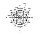
- FIG. 4 is a diagram for explaining the radiation characteristics of the antenna device having a square shape when viewed from the top surface according to the embodiment of the present invention.
- a waveform 270 indicates vertical polarization
- a waveform 280 indicates horizontal polarization.
- the volume constituting the antenna element can be set to 17 mm on one side of the square forming the antenna element 210 and the height of each leg can be 4 mm.
- the size can be reduced as compared with the element.
- the antenna element 110 is described as a regular triangle and the antenna element 210 is a square.
- various shapes may be used within the range of a regular polygon.
- it may not be a regular polygon as long as it is a point symmetric structure.
- the antenna device may be circular.
- the antenna element 110 and the antenna element 210 are not necessarily flat, and the antenna element 110 and the antenna element 210 may have a curved structure as long as the point-symmetric structure is maintained.
- FIG. 5 is a diagram showing a current distribution on the top surface in the case of a configuration similar to a slot antenna.
- a power feeding unit is provided on the top surface and the four legs are grounded.
- the current on the top surface is canceled in a complicated manner, and the size of the side surface opening (slot) becomes a behavior that depends on the operating frequency.
- the current distribution becomes a distribution that is biased toward the central portion and the end portion. More specifically, as shown in the distribution 510, there are portions where the arrows strengthen each other and cancel each other. For the parts that cancel each other, the magnitude of the current is cancelled.
- FIG. 6 is a diagram showing a current distribution on the top surface in the case of a configuration similar to a loop antenna.
- the current distribution when the antenna device is configured as shown in FIG. 3 and a current is supplied will be described with reference to FIG.
- this configuration as shown by a distribution 600 in FIG. 6, this is an operation in which a current flows from the center portion of the top surface portion to the side surface opening portion. More specifically, as shown in the distribution 610, there are fewer portions where the arrows cancel each other than in the case of FIG. 5, and the current distribution is uniform as a whole.
- the feed point is arranged on any one of the top side, and is operated as a slot antenna.
- the feed point is arranged on one of the leg portions. It can be operated as a loop antenna, thereby increasing the current efficiency, and as a result, downsizing and thinning can be realized.
- FIG. 7 is a diagram for explaining an antenna device having a cutout shape on the outer side according to the embodiment of the present invention.
- FIG. 7 shows a shape in which the outer side portion of the antenna element 210 shown in FIG. 3 is cut out.
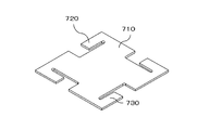
- the antenna device of FIG. 7 is disposed on a flat plate-like grounded wiring substrate 700, a flat plate-like antenna element 710 disposed to face the wiring substrate 700 with a space therebetween, and an end of the antenna element 710.
- Each of the extension destinations includes three grounding legs 720 that are connected to the wiring board 700, and a power feeding leg 730 that is arranged at the end of the antenna element 710 and whose extension destination is connected to the circuit 750.
- the antenna device shown in FIG. 7 connects between the ends of the antenna element 710 where any two of the plurality of grounding legs 720 and the feeding legs 730 are arranged. Further provided is a notch portion 760 in which each of the outer side portions is cut out at least partially. The plurality of grounding leg portions 720 and the power feeding leg portions 730 are connected from the extension destinations of the portions that are not cut out for each of the outer side portions.
- the cutout portion 760 is a portion cut from the antenna element 710, and when notched by the cutout portion 760 that is the cut portion, the antenna device including the antenna element 710 is the antenna device shown in FIG. It becomes the same as the configuration.
- the shape of the notch 760 is a rectangle having a length from the center point of each outer side of the antenna element 710 toward one direction of the apex, with the length from the center point as one piece.
- Another piece of the notch 710 is a portion extending vertically from the outer side portion, that is, toward the center of gravity of the antenna element 710, and is shorter than a portion along the outer side portion.
- the above cutout portions 760 are provided on each of the four sides of the antenna element 710.
- the antenna element 710 as a whole has a point-symmetric structure even after the cutout portion 760 is provided.
- the four notches 760 are arranged so as to be point-symmetric as a whole, and when a notch 760 is shifted to the left on the outer side, the other three outer sides are also shifted to the left.
- the notch portion 760 in FIG.
- the outer sides after being cut out may be further extended, or conversely shortened.
- the structure is appropriate so that the current and electric field have the desired distribution.
- FIG. 8 is a diagram showing a configuration before assembling the antenna device according to the embodiment of the present invention.
- FIG. 7 shows the arrangement relationship of the antenna device including the antenna element 710
- the shape for forming the antenna element 710 shown in FIG. 7 will be described with reference to FIG.
- four portions of the square antenna element 210 shown in FIG. 3 may be cut out and further leg portions may be arranged.
- the three portions extending from the apex are the grounding leg portions 720, and the other one portion forms the power feeding leg portion 730.
- These legs are arranged as shown in FIG. 7 by bending them at right angles.
- the antenna apparatus shown in FIG. 7 also has a basic operation of a deformed loop antenna of about 1 ⁇ having vertical polarization and omnidirectional radiation characteristics as in FIG. With this configuration, non-directional radiation characteristics can be obtained.
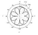
- FIG. 9 is a diagram for explaining the radiation characteristics of the antenna device having a notch according to the embodiment of the present invention.
- a waveform 770 indicates vertical polarization
- a waveform 780 indicates horizontal polarization.
- the volume constituting the antenna element can be set to 15.8 mm for one side of the square forming the antenna element 210 and 4 mm for each leg.
- the antenna element can be downsized as compared with the antenna element. In this way, by forming slits and bent sides that serve as detours for high-frequency currents in the vicinity of the grounding leg 720 and the power feeding leg 730, the antenna's radiation characteristics and operating frequency can be maintained while maintaining the antenna's The projected area can be reduced.
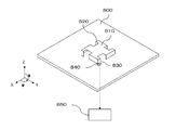
- FIG. 10 is a diagram for explaining a second antenna device having a cutout shape on the outer side according to the embodiment of the present invention and a leg portion having a width.
- FIG. 7 shows the antenna device provided with the notch portion 760
- FIG. 10 will explain the antenna device having a wider leg portion.
- the antenna device of FIG. 10 is arranged at a flat grounded wiring board 800, a flat antenna element 810 disposed to face the wiring board 800 at an interval, and an end of the antenna element 810.
- Three grounding legs 820 each having an extension destination connected to the wiring board 800, and a power feeding leg 830 that is arranged at an end of the antenna element 810 and whose extension destination is connected to the circuit 850.
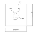
- FIG. 11 is a diagram showing a second antenna device according to an embodiment of the present invention, which has a cutout shape on the outer side and has a leg portion with a width, from the upper part and the side part.
- each of the outer edge portions connecting the end portions where any two adjacent ones of the plurality of grounding leg portions 820 and the feeding leg portions 830 are arranged in the antenna element 810 is cut.
- a cutout portion 860 having a cutout shape is further provided.
- the plurality of grounding leg portions 820 and the power feeding leg portions 830 are formed in a planar shape extending from a portion that is not cut out of each outer side portion.
- the configuration of the antenna device shown in FIG. 10 is basically the same as the configuration of the antenna device shown in FIG. 7, but is different in that the legs are formed on the surface. With this configuration, the leg portion is stabilized, so that the antenna device as a whole is structurally stable, and the capacity between the antenna element and the ground plane is increased, so that the overall size can be further reduced.
- the antenna apparatus shown in FIG. 10 also has a basic operation of a deformed loop antenna of about 1 ⁇ having vertical polarization and omnidirectional radiation characteristics as in FIG. With this configuration, non-directional radiation characteristics can be obtained.
- FIG. 12 is a diagram for explaining the radiation characteristics of the second antenna device provided with the notches according to the embodiment of the present invention.
- a waveform 870 indicates vertical polarization
- a waveform 880 indicates horizontal polarization.
- the volume of the antenna element can be 15 mm on one side of the square forming the antenna element 210 and the height of each leg can be 4 mm. The size can be reduced as compared with the element.
- the antenna device including two or three grounding legs is illustrated, but the number of grounding legs may be four or more.
- the display device according to the present invention is useful for a vehicle antenna device, but is not limited to a vehicle and can also be applied to antenna devices used for many purposes.
Landscapes
- Waveguide Aerials (AREA)
- Details Of Aerials (AREA)
- Engineering & Computer Science (AREA)
- Remote Sensing (AREA)
Abstract
平板状の接地された配線基板100と、配線基板100に対して間隔を空けて対向配置された平板状のアンテナ素子110と、アンテナ素子110の端部に配され、それぞれの延伸先が配線基板100に接続される2つの接地用脚部120と、アンテナ素子110の端部に配され、延伸先が回路150(送信回路又は受信回路)に接続される給電用脚部130を備える。複数の接地用脚部120が配されるそれぞれの端部と、給電用脚部130が配される端部とにより形成される面は点対称である。
Description
本発明は、アンテナ装置に関する。
近年、自動車のルーフトップにアンテナ装置を搭載して通信する構成が広く用いられている。自動車から地上インフラと通信する用途では、水平面内で無指向性の指向性を持つ、垂直偏波のモノポールタイプ又はダイポールタイプのアンテナが多く利用されている。
モノポールタイプ又はダイポールタイプのアンテナは、通常λ/4~λ/2程度のアンテナ高を要するため、外装ケースの高さが増してしまう。例えば5.9GHz帯のアンテナの場合、12mm程度の高さとなる。また、その形状故に素子の自立が困難で形状が安定しないため、ほとんどの場合がアンテナの保持部材を必要としていた。
これに対し、特許文献1では、方位角に対して無指向性の垂直偏波アンテナとして動作する薄型のアンテナ装置が開示されている。具体的には、一対の平板状導体の相対向する周縁部の間に左右が接続導体で仕切られた開口が形成され、給電時に該開口内の電界分布はスロットアンテナと類似したものとなるため、該開口の前方へ垂直偏波を放射させている。
一方でアンテナ装置はさらなる小型化が求められている。特許文献1のアンテナ装置によると、天面部の電流が複雑にキャンセルされる。スロットアンテナと類似した動作をすることから、少なくとも20x20x4mm(1600mm2)程度の大きさを確保しなければ、十分な電波受信が確保されず、十分に小型化することができなかった。
本発明はかかる事情に鑑みてなされたものであり、その目的は、無指向性の垂直偏波アンテナについて、さらに小型化されたアンテナ装置を提供することにある。
本発明に係るアンテナ装置は、接地された配線基板に対して間隔を空けて対向配置された平板状のアンテナ素子と、前記アンテナ素子の端部に配され、それぞれの延伸先が前記配線基板に接続される複数の接地用脚部と、前記アンテナ素子の端部に配され、延伸先が送信回路又は受信回路に接続される給電用脚部を備え、前記複数の接地用脚部が配されるそれぞれの端部と、前記給電用脚部が配される端部とにより形成される面は点対称である。
この構成によれば、点対称となる形状の一端から給電され、他端で接地することから、電流分布が回転対称でループ動作し、電流が複雑にキャンセルしあう状況を解消することができる。その結果、適切な大きさの動作長を確保することができるので、動作長の大きさを確保しつつも小型化を実現することができる。
好適には、前記アンテナ素子の前記配線基板に対向する面は正多角形であり、前記給電用脚部が配される端部は、前記正多角形の頂点の1つであり、前記複数の接地用脚部が配される端部は、前記正多角形の他の頂点である。
この構成によれば、単純な構造で設計、製造しやすい形でアンテナ素子の点対称構造を実現することができる。そして点対称構造とすることにより、アンテナ素子の小型化を実現することができる。
好適には、前記アンテナ素子のうち、前記複数の接地用脚部と前記給電用脚部のうち隣接するいずれか2つが配される端部の間を結ぶ外辺部分のそれぞれを、少なくとも一部において切り欠いた形状とする切り欠き部をさらに備え、前記複数の接地用脚部及び前記給電用脚部は、前記外辺部分のそれぞれについて切り欠かれていない部分の延伸先から接続される。
この構成によれば、点対称構造により電流分布をループさせた形状にさらに切り欠き部を備えるので、切り欠き部により外辺部分周辺に流れるはずの電流が蛇行し、その結果電流経路をさらに確保することができることから、さらなる小型化を実現することができる。
好適には、前記複数の接地用脚部と前記給電用脚部は、前記それぞれの外辺部分のうち切り欠かれていない部分から延びて面状に形成される。
この構成によれば、接地用脚部と前記給電用脚部が配線基板に近接することから、アンテナ素子と接地面との容量が大きくなるように接地され、さらなる小型化を実現することができる。
好適には、前記アンテナ素子の前記配線基板に対向する面は正三角形又は正四角形である。
この構成によれば、正多角形のうちで特に小型化しやすく、製造しやすい形とすることができる。
好適には、前記アンテナ素子の前記配線基板に対向する面は、切り欠き前の形状が正三角形又は正四角形である。
この構成によれば、製造しやすい形状をベースにして電流の蛇行形状を実現することができ、それにより小型化を実現することができる。
好適には、前記配線基板をさらに備え、前記配線基板は平板状である。
この構成によれば、アンテナ素子と配線基板の組み合わせにより、無指向性の垂直偏波アンテナを実現することができる。
本発明によれば、無指向性の垂直偏波アンテナについて、さらに小型化されたアンテナ装置を提供することができる。
図1は、本発明の実施の形態に係る天面から見た場合に三角形状となるアンテナ装置を説明する図である。図1に示す三角形状となるアンテナ装置は、平板状の接地された配線基板100と、配線基板100に対して間隔を空けて対向配置された平板状のアンテナ素子110と、アンテナ素子110の端部に配され、それぞれの延伸先が配線基板100に接続される2つの接地用脚部120と、アンテナ素子110の端部に配され、延伸先が回路150(送信回路又は受信回路)に接続される給電用脚部130を備える。
アンテナ素子110は、天面側(上面)とその裏側(下面)から見たときにそれぞれ平面となるような平板上の形状を有している。上面と下面をそれぞれ形成する図形は、同じ形であり、上面と下面の間は一定の厚さを有している。アンテナ素子110の上面及び下面は、中心点111を中心とした点対称図形であり、正多角形である。図1の例では、アンテナ素子110の上面及び下面を正三角形として説明する。
アンテナ素子110の上面は正三角形であるので、3つの頂点を有する。図1の例では、この3つの頂点を端部として説明する。この3つの頂点、端部を結ぶことにより形成される図形は点対称図形であり、正多角形である。図1の例では、アンテナ素子110の上面の図形と同じく、正三角形である。
2つの接地用脚部120は、アンテナ素子110の2つの端部、アンテナ素子110の3つの頂点のうちの2つに配される。そして、2つの接地用脚部120はそれぞれ、アンテナ素子110の上面及び下面から垂直、法線方向に延び、それぞれの延伸先が配線基板100に接続される。2つの接地用脚部120はそれぞれ、配線基板100に対しても垂直、法線方向から到達し、それぞれの延伸先が配線基板100に接続される。
給電用脚部130は、アンテナ素子110の端部の1つ、アンテナ素子110の3つの頂点のうちの残り1つに配される。そして、給電用脚部130はそれぞれ、アンテナ素子110の上面及び下面から垂直、法線方向に延び、それぞれの延伸先が配線基板100に垂直、法線方向から向かう。配線基板100のうち、給電用脚部130の向かう先には穴140があけられており、給電用脚部130は、配線基板100の接地部に接しないように配線基板100の面を通過する。
給電用脚部130は、最終的に回路150(送信回路又は受信回路)に接続される。複数の接地用脚部120が配されるそれぞれの端部と、給電用脚部130が配される端部とにより形成される面は点対称である。回路150からは、給電線を介してアンテナ装置に対して給電される。
上述のようにアンテナ装置を接地した状態で給電すると、図1に示す矢印の流れに沿って電流が流れる。給電した結果として電流は、アンテナ素子110の上面の重心部分から各頂点に向かって流れる。また三辺の中心から各頂点に向かって電流が流れる。このように各頂点に向かって電流が流れ、各頂点から各脚部を配線基板100に向かって電流が流れる。配線基板100に到達した電流は、配線基板100でアンテナ素子110の上面とは逆向きに流れる。
図1に示したアンテナ装置では、アンテナ素子110により4方向に約λ/2の開口部を持つ変形ループアンテナが形成され、低姿勢で自立可能な、かつ垂直偏波で無指向性の放射特性をもつアンテナ装置を構成する。基本動作は、約1λのループアンテナであり、アンテナ素子110の天面形状とGNDである配線基板100と接続する2つの接地用脚部120、および給電用脚部130を点対象に構成することで、無指向性の放射特性を得ることができる。図2は、本発明の実施の形態に係る天面から見た場合に三角形状となるアンテナ装置の放射特性を説明する図である。波形170は垂直偏波を示し波形180は水平偏波を示す。
5.9GHzで動作するアンテナを例とすると、アンテナ素子を構成する容積は、アンテナ素子110を形成する正三角形の一辺を17.3mmと、各脚部の高さを4.5mmとすることができる。従来のアンテナ素子の天面部中心に給電部を設ける構造では、一辺20mm程度としなければならなかったアンテナ装置と比べて小型化することができ、約38%の小型化を実現することができる。なお、辺と高さと波長の関係については、横+縦=λ/2となるように構成するのが望ましい。
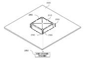
図3は、本発明の実施の形態に係る天面から見た場合に正方形状となるアンテナ装置を説明する図である。図3は、図1に示したアンテナ装置の上面及び下面の形状を正三角形に替えて正方形にしたものである。図3に示す正方形状となるアンテナ装置は、平板状の接地された配線基板200と、配線基板200に対して間隔を空けて対向配置された平板状のアンテナ素子210と、アンテナ素子210の端部に配され、それぞれの延伸先が配線基板200に接続される3つの接地用脚部220と、アンテナ素子210の端部に配され、延伸先が回路250に接続される給電用脚部230を備える。
アンテナ素子210の上面は正方形であるので、4つの頂点を有する。図3の例では、この4つの頂点を端部として説明する。図3の例では、この4つの頂点、端部を結ぶことにより形成される図形は、アンテナ素子210の上面の図形と同じく、正方形である。
3つの接地用脚部220は、アンテナ素子210の2つの端部、アンテナ素子210の4つの頂点のうちの3つに配される。そして、3つの接地用脚部220はそれぞれ、アンテナ素子210の上面及び下面から垂直、法線方向に延び、それぞれの延伸先が配線基板200に接続される。2つの接地用脚部220はそれぞれ、配線基板200に対しても垂直、法線方向から到達し、それぞれの延伸先が配線基板200に接続される。
給電用脚部230は、アンテナ素子210の端部の1つ、アンテナ素子210の4つの頂点のうちの残り1つに配される。そして、給電用脚部230はそれぞれ、アンテナ素子210の上面及び下面から垂直、法線方向に延び、それぞれの延伸先が配線基板200に垂直、法線方向から向かう。配線基板200のうち、給電用脚部230の向かう先には穴240があけられており、給電用脚部230は、配線基板200の接地部に接しないように配線基板200の面を通過する。給電用脚部230は、最終的に給電先である回路250(送信回路又は受信回路)に接続され、給電線を介してアンテナ装置に対して給電される。
上述のようにアンテナ装置を接地した状態で給電すると、図3に示す矢印の流れに沿って電流が流れる。給電した結果として電流は、アンテナ素子210の上面の重心部分から各頂点に向かって流れる。また四辺の中心から各頂点に向かって電流が流れる。このように各頂点に向かって電流が流れ、各頂点から各脚部を配線基板200に向かって電流が流れる。配線基板200に到達した電流は、配線基板200でアンテナ素子210の上面とは逆向きに流れる。
図3に示したアンテナ装置も、図1と同様に垂直偏波で無指向性の放射特性をもつ約1λの変形ループアンテナを基本動作とする。このように構成することで、無指向性の放射特性を得ることができる。図4は、本発明の実施の形態に係る天面から見た場合に正方形状となるアンテナ装置の放射特性を説明する図である。波形270は垂直偏波を示し、波形280は水平偏波を示す。
5.9GHzで動作するアンテナを例とすると、アンテナ素子を構成する容積は、アンテナ素子210を形成する正方形の一辺を17mmと、各脚部の高さを4mmとすることができ、従来のアンテナ素子と比べて小型化できる。
図1及び図3の例では、アンテナ素子110を正三角形と、アンテナ素子210を正方形として説明したが、正多角形の範囲内で様々な形状としてもよい。また、点対称構造とすることで電流分布をループ動作させる関係上、点対称構造で
あれば正多角形でなくてもよく、例えばアンテナ装置を円形としてもよい。またアンテナ素子110及びアンテナ素子210は必ずしも平面である必要はなく、点対称構造が維持される限り、アンテナ素子110及びアンテナ素子210を曲面構造としてもよい。
あれば正多角形でなくてもよく、例えばアンテナ装置を円形としてもよい。またアンテナ素子110及びアンテナ素子210は必ずしも平面である必要はなく、点対称構造が維持される限り、アンテナ素子110及びアンテナ素子210を曲面構造としてもよい。
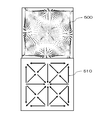
図5は、スロットアンテナに類する形態の場合の天面部の電流分布を示す図である。図3に示したようにアンテナ装置を構成して電流を流した場合の電流分布を説明する前に、天面部に給電部を設けて4本の脚部を接地した構成にした場合の例について説明する。この従来の構成の場合、図5の分布500に示すように、天面部の電流が複雑にキャンセルされ、側面開口部(スロット)の大きさが、動作周波数に依存する振る舞いとなる。その結果、電流分布が中心部分と端部に偏った分布となる。より具体的には分布510に示すように、矢印同士が強め合う部分と打ち消し合う部分が生じる。打ち消し合う部分については、電流の大きさがキャンセルされる。
図6は、ループアンテナに類する形態の場合の天面部の電流分布を示す図である。図5に示した場合に替えて、図3に示したようにアンテナ装置を構成して電流を流した場合の電流分布を図6を参照して説明する。この構成の場合、図6の分布600に示すように、天面部中心部分から側面開口部にかけて、電流が流れる動作であり、小型でありながら動作長を拡大する振る舞いとなる。より具体的には分布610に示すように、矢印同士が打ち消し合う部分が図5の場合に比べて少なくなり、全体として電流分布が均一となる。
上述の構成により、給電点を天面側のいずれかに配置することでスロットアンテナとして動作させていたところを、本実施の形態では、給電点を脚部の1つに配置することにより、変形ループアンテナとして動作させ、それにより電流の効率を上げ、その結果として小型化、薄型化を実現することができる。
図7は、本発明の実施の形態に係る外辺に切り欠き形状を備えたアンテナ装置を説明する図である。図7は、図3に示したアンテナ素子210の外辺部を切り欠いた形状としたものである。図7のアンテナ装置は、平板状の接地された配線基板700と、配線基板700に対して間隔を空けて対向配置された平板状のアンテナ素子710と、アンテナ素子710の端部に配され、それぞれの延伸先が配線基板700に接続される3つの接地用脚部720と、アンテナ素子710の端部に配され、延伸先が回路750に接続される給電用脚部730を備える。
図7に示したアンテナ装置は上記の構成に加え、アンテナ素子710のうち、複数の接地用脚部720と給電用脚部730のうち隣接するいずれか2つが配される端部の間を結ぶ外辺部分のそれぞれを、少なくとも一部において切り欠いた形状とする切り欠き部760をさらに備える。そして、複数の接地用脚部720及び給電用脚部730は、外辺部分のそれぞれについて切り欠かれていない部分の延伸先から接続される。
切り欠き部760はアンテナ素子710から切断された部分であり、この切断部分である切り欠き部760により切り欠かれていない場合、アンテナ素子710を含むアンテナ装置は、図3に示したアンテナ装置の構成と同一となる。切り欠き部760の形状は、アンテナ素子710の各外辺の中心点から、頂点の1つの方向に向かいつつ、その手前までの長さを一片とする長方形である。切り欠き部710の他の一片は、外辺部分から垂直に、すなわちアンテナ素子710の重心に向かって延びる部分であり、外辺部分に沿った部分よりも短い。
以上の切り欠き部760が、アンテナ素子710の四辺のそれぞれに設けられ、その結果として全体としてアンテナ素子710は切り欠き部760を備えた後も点対称の構造となる。したがって4つの切り欠き部760は、全体として点対称となるように配置し、ある切り欠き部760が外辺上で左に寄っている場合、他の3つの外辺でもそれぞれ左に寄った位置に切り欠き部760を配置することで全体として点対称構造とする。なお、全体として点対称構造となればよいので、切り欠かれた後の外辺をそれぞれさらに延ばした構造としてもよく、逆に短縮した構造としてもよい。電流、電界が所望の分布となるような適切な構造とする。
図8は、本発明の実施の形態に係るアンテナ装置を組み立てる前の構成を示す図である。図7ではアンテナ素子710を含むアンテナ装置の配置関係を示したが、図7に示すアンテナ素子710を形成するための形状について図8を参照して説明する。もちろん図3に示した正方形のアンテナ素子210のうち4か所を切り欠いてさらに脚部を配置してもよいが、図8に示すように切り欠き部760のうち頂点に近い部分から延びる部分を切り欠かずない構成とすることもできる。この場合、頂点から延びる3つの部分がそれぞれ接地用脚部720であり、他の1つの部分が給電用脚部730を形成する。これらの脚部は、いずれも直角に折り曲げることにより、図7に示した配置となる。
図7に示したアンテナ装置も、図1と同様に垂直偏波で無指向性の放射特性をもつ約1λの変形ループアンテナを基本動作とする。このように構成することで、無指向性の放射特性を得ることができる。図9は、本発明の実施の形態に係る切り欠きを備えたアンテナ装置の放射特性を説明する図である。波形770は垂直偏波を示し、波形780は水平偏波を示す。
5.9GHzで動作するアンテナを例とすると、アンテナ素子を構成する容積は、アンテナ素子210を形成する正方形の一辺を15.8mmと、各脚部の高さを4mmとすることができ、従来のアンテナ素子と比べて小型化できる。このように、接地用脚部720、給電用脚部730近傍に、高周波電流の迂回路となるスリットや、折り曲げ辺を構成することで、アンテナの放射特性と動作周波数を維持しながら、アンテナの投影面積の縮小ができる。
図10は、本発明の実施の形態に係る外辺に切り欠き形状を備えた上に脚部に幅を持たせた第2のアンテナ装置を説明する図である。図7では、切り欠き部760を備えたアンテナ装置について示したが、図10ではこれをさらに脚部を幅広くしたものについて説明する。図10のアンテナ装置は、平板状の接地された配線基板800と、配線基板800に対して間隔を空けて対向配置された平板状のアンテナ素子810と、アンテナ素子810の端部に配され、それぞれの延伸先が配線基板800に接続される3つの接地用脚部820と、アンテナ素子810の端部に配され、延伸先が回路850に接続される給電用脚部830を備える。図11は、本発明の実施の形態に係る、外辺に切り欠き形状を備えた上に脚部に幅を持たせた第2のアンテナ装置を上部と側部から示す図である。
さらに、アンテナ素子810のうち、複数の接地用脚部820と給電用脚部830のうち隣接するいずれか2つが配される端部の間を結ぶ外辺部分のそれぞれを、少なくとも一部において切り欠いた形状とする切り欠き部860をさらに備える。そして、複数の接地用脚部820及び給電用脚部830は、それぞれの外辺部分のうち切り欠かれていない部分から延びて面状に形成される。
このように、図10に示したアンテナ装置の構成は基本的には図7に示したアンテナ装置の構成と同じであるが、脚部が面上に形成される点で異なる。このように構成することにより、脚部が安定するのでアンテナ装置全体として構造的に安定するとともに、アンテナ素子と接地面との容量が大きくなるため、全体としてさらに小型化することができる。
図10に示したアンテナ装置も、図1と同様に垂直偏波で無指向性の放射特性をもつ約1λの変形ループアンテナを基本動作とする。このように構成することで、無指向性の放射特性を得ることができる。図12は、本発明の実施の形態に係る切り欠きを備えた第2のアンテナ装置の放射特性を説明する図である。波形870は垂直偏波を示し、波形880は水平偏波を示す。5.9GHzで動作するアンテナを例とすると、アンテナ素子を構成する容積は、アンテナ素子210を形成する正方形の一辺を15mmと、各脚部の高さを4mmとすることができ、従来のアンテナ素子と比べて小型化できる。
以上のように、各図を参照して点対称構造を採用し、脚部の1つを接地部分に替えて給電用の構成とした場合について説明した。この構成によれば、点対称となる形状の一端から給電され、他端で接地することから、電流分布が回転対称でループ動作し、電流が複雑にキャンセルしあう状況を解消することができる。その結果、適切な大きさの動作長を確保することができるので、動作長の大きさを確保しつつも小型化を実現することができる。
本発明は上述した実施形態には限定されない。すなわち、当業者は、本発明の技術的範囲またはその均等の範囲内において、上述した実施形態の構成要素に関し、様々な変更、コンビネーション、サブコンビネーション、並びに代替を行ってもよい。本発明について上記実施形態を参照しつつ説明したが、本発明は上記実施形態に限定されるものではなく、改良の目的または本発明の思想の範囲内において改良または変更が可能である。
例えば、上述した実施形態では、2つあるいは3つの接地用脚部を備えたアンテナ装置を例示したが、接地用脚部は4つ以上であってもよい。
以上のように、本発明に係る表示装置は、車両用のアンテナ装置に有用であるが、車両用に限らず多くの用途に用いられるアンテナ装置にも適用することができる。
100…配線基板
110…アンテナ素子
120…接地用脚部
130…給電用脚部
140…穴
150…回路
200…配線基板
210…アンテナ素子
220…接地用脚部
230…給電用脚部
250…回路
700…配線基板
710…アンテナ素子
720…接地用脚部
730…給電用脚部
750…回路
760…切り欠き部
800…配線基板
810…アンテナ素子
820…接地用脚部
830…給電用脚部
850…回路
860…切り欠き部
110…アンテナ素子
120…接地用脚部
130…給電用脚部
140…穴
150…回路
200…配線基板
210…アンテナ素子
220…接地用脚部
230…給電用脚部
250…回路
700…配線基板
710…アンテナ素子
720…接地用脚部
730…給電用脚部
750…回路
760…切り欠き部
800…配線基板
810…アンテナ素子
820…接地用脚部
830…給電用脚部
850…回路
860…切り欠き部
Claims (7)
- 接地された配線基板に対して間隔を空けて対向配置された平板状のアンテナ素子と、
前記アンテナ素子の端部に配され、それぞれの延伸先が前記配線基板に接続される複数の接地用脚部と、
前記アンテナ素子の端部に配され、延伸先が送信回路又は受信回路に接続される給電用脚部を備え、
前記複数の接地用脚部が配されるそれぞれの端部と、前記給電用脚部が配される端部とにより形成される面は点対称である、
アンテナ装置。 - 前記アンテナ素子の前記配線基板に対向する面は正多角形であり、
前記給電用脚部が配される端部は、前記正多角形の頂点の1つであり、
前記複数の接地用脚部が配される端部は、前記正多角形の他の頂点である、
請求項1に記載のアンテナ装置。 - 前記アンテナ素子のうち、前記複数の接地用脚部と前記給電用脚部のうち隣接するいずれか2つが配される端部の間を結ぶ外辺部分のそれぞれを、少なくとも一部において切り欠いた形状とする切り欠き部をさらに備え、
前記複数の接地用脚部及び前記給電用脚部は、前記外辺部分のそれぞれについて切り欠かれていない部分の延伸先から接続される、
請求項1又は請求項2に記載のアンテナ装置。 - 前記複数の接地用脚部及び前記給電用脚部は、前記それぞれの外辺部分のうち切り欠かれていない部分から延びて面状に形成される、
請求項3に記載のアンテナ装置。 - 前記アンテナ素子の前記配線基板に対向する面は正三角形又は正四角形である、
請求項2に記載のアンテナ装置。 - 前記アンテナ素子の前記配線基板に対向する面は、切り欠き前の形状が正三角形又は正四角形である、
請求項3又は請求項4に記載のアンテナ装置。 - 前記配線基板をさらに備え、前記配線基板は平板状である、
請求項1~請求項6のいずれかに記載のアンテナ装置。
Priority Applications (4)
| Application Number | Priority Date | Filing Date | Title |
|---|---|---|---|
| JP2017547745A JP6474069B2 (ja) | 2015-10-26 | 2016-10-18 | アンテナ装置 |
| EP16859640.1A EP3370305B1 (en) | 2015-10-26 | 2016-10-18 | Antenna device |
| CN201680058968.7A CN108140952B (zh) | 2015-10-26 | 2016-10-18 | 天线装置 |
| US15/910,213 US10411355B2 (en) | 2015-10-26 | 2018-03-02 | Antenna device |
Applications Claiming Priority (2)
| Application Number | Priority Date | Filing Date | Title |
|---|---|---|---|
| JP2015209786 | 2015-10-26 | ||
| JP2015-209786 | 2015-10-26 |
Related Child Applications (1)
| Application Number | Title | Priority Date | Filing Date |
|---|---|---|---|
| US15/910,213 Continuation US10411355B2 (en) | 2015-10-26 | 2018-03-02 | Antenna device |
Publications (1)
| Publication Number | Publication Date |
|---|---|
| WO2017073410A1 true WO2017073410A1 (ja) | 2017-05-04 |
Family
ID=58630082
Family Applications (1)
| Application Number | Title | Priority Date | Filing Date |
|---|---|---|---|
| PCT/JP2016/080867 Ceased WO2017073410A1 (ja) | 2015-10-26 | 2016-10-18 | アンテナ装置 |
Country Status (5)
| Country | Link |
|---|---|
| US (1) | US10411355B2 (ja) |
| EP (1) | EP3370305B1 (ja) |
| JP (1) | JP6474069B2 (ja) |
| CN (1) | CN108140952B (ja) |
| WO (1) | WO2017073410A1 (ja) |
Families Citing this family (3)
| Publication number | Priority date | Publication date | Assignee | Title |
|---|---|---|---|---|
| US10930993B2 (en) * | 2017-01-20 | 2021-02-23 | Sony Semiconductor Solutions Corporation | Antenna device and reception device |
| WO2018135060A1 (ja) | 2017-01-20 | 2018-07-26 | ソニーセミコンダクタソリューションズ株式会社 | アンテナ装置及び受信装置 |
| EP3977558A1 (en) * | 2019-05-29 | 2022-04-06 | Robert Bosch GmbH | An antenna system |
Citations (5)
| Publication number | Priority date | Publication date | Assignee | Title |
|---|---|---|---|---|
| JPH0537229A (ja) * | 1991-07-26 | 1993-02-12 | Harada Ind Co Ltd | マイクロストリツプアンテナ |
| JPH09153730A (ja) * | 1995-11-29 | 1997-06-10 | Kyocera Corp | 平面アンテナ |
| JP2003188620A (ja) * | 2001-12-19 | 2003-07-04 | Murata Mfg Co Ltd | モジュール一体型アンテナ |
| JP2006135773A (ja) * | 2004-11-08 | 2006-05-25 | Alps Electric Co Ltd | アンテナ装置 |
| JP2008219578A (ja) * | 2007-03-06 | 2008-09-18 | Nippon Soken Inc | パッチアンテナ |
Family Cites Families (16)
| Publication number | Priority date | Publication date | Assignee | Title |
|---|---|---|---|---|
| EP0777295B1 (en) * | 1995-11-29 | 2003-05-28 | Ntt Mobile Communications Network Inc. | Antenna device having two resonance frequencies |
| US6448933B1 (en) * | 2001-04-11 | 2002-09-10 | Tyco Electronics Logisitics Ag | Polarization and spatial diversity antenna assembly for wireless communication devices |
| US6448932B1 (en) * | 2001-09-04 | 2002-09-10 | Centurion Wireless Technologies, Inc. | Dual feed internal antenna |
| JP4234957B2 (ja) * | 2001-10-30 | 2009-03-04 | 株式会社リコー | ズームレンズ、撮像装置および携帯情報端末システム |
| US20030107881A1 (en) * | 2001-12-11 | 2003-06-12 | Ngk Insulators, Ltd. | Setting construction of shield case or planar antenna on circuit board |
| US7046199B2 (en) * | 2003-02-13 | 2006-05-16 | Skycross, Inc. | Monolithic low profile omni-directional surface-mount antenna |
| JP2004336237A (ja) * | 2003-05-02 | 2004-11-25 | Tadashi Nakamura | 円偏波平面アンテナ |
| JP2005039754A (ja) * | 2003-06-26 | 2005-02-10 | Alps Electric Co Ltd | アンテナ装置 |
| JP3959068B2 (ja) * | 2003-11-12 | 2007-08-15 | アルプス電気株式会社 | 円偏波アンテナ |
| JP4217596B2 (ja) * | 2003-12-05 | 2009-02-04 | アルプス電気株式会社 | アンテナ一体型モジュール |
| US7183985B2 (en) * | 2005-07-08 | 2007-02-27 | Universal Scientific Industrial Co., Ltd. | Planar inverted-F antenna |
| US20080143608A1 (en) * | 2006-12-13 | 2008-06-19 | Alps Electric Co., Ltd. | Antenna-integrated module |
| JP4910197B2 (ja) * | 2008-03-19 | 2012-04-04 | Dxアンテナ株式会社 | アンテナ装置 |
| JP2012147263A (ja) * | 2011-01-12 | 2012-08-02 | Sony Corp | アンテナ・モジュール並びに無線通信装置 |
| DE102012014913A1 (de) * | 2012-07-29 | 2014-05-15 | Heinz Lindenmeier | Elektrisch kleiner Strahler für vertikal polarisierte Funksignale |
| CN106486741B (zh) * | 2015-08-26 | 2020-04-17 | 香港中文大学 | 一种空气贴片微带天线 |
-
2016
- 2016-10-18 WO PCT/JP2016/080867 patent/WO2017073410A1/ja not_active Ceased
- 2016-10-18 EP EP16859640.1A patent/EP3370305B1/en active Active
- 2016-10-18 CN CN201680058968.7A patent/CN108140952B/zh active Active
- 2016-10-18 JP JP2017547745A patent/JP6474069B2/ja active Active
-
2018
- 2018-03-02 US US15/910,213 patent/US10411355B2/en active Active
Patent Citations (5)
| Publication number | Priority date | Publication date | Assignee | Title |
|---|---|---|---|---|
| JPH0537229A (ja) * | 1991-07-26 | 1993-02-12 | Harada Ind Co Ltd | マイクロストリツプアンテナ |
| JPH09153730A (ja) * | 1995-11-29 | 1997-06-10 | Kyocera Corp | 平面アンテナ |
| JP2003188620A (ja) * | 2001-12-19 | 2003-07-04 | Murata Mfg Co Ltd | モジュール一体型アンテナ |
| JP2006135773A (ja) * | 2004-11-08 | 2006-05-25 | Alps Electric Co Ltd | アンテナ装置 |
| JP2008219578A (ja) * | 2007-03-06 | 2008-09-18 | Nippon Soken Inc | パッチアンテナ |
Non-Patent Citations (1)
| Title |
|---|
| See also references of EP3370305A4 * |
Also Published As
| Publication number | Publication date |
|---|---|
| EP3370305A1 (en) | 2018-09-05 |
| EP3370305A4 (en) | 2018-09-26 |
| EP3370305B1 (en) | 2020-12-09 |
| JPWO2017073410A1 (ja) | 2018-07-26 |
| US10411355B2 (en) | 2019-09-10 |
| CN108140952B (zh) | 2020-06-23 |
| US20180191070A1 (en) | 2018-07-05 |
| JP6474069B2 (ja) | 2019-02-27 |
| CN108140952A (zh) | 2018-06-08 |
Similar Documents
| Publication | Publication Date | Title |
|---|---|---|
| CN103915678B (zh) | 全向式天线 | |
| EP1814193B1 (en) | Planar antenna | |
| CN104396085B (zh) | 多输入多输出天线及其宽带偶极子辐射元件 | |
| JP4571196B2 (ja) | 偏波ダイバーシチアンテナ | |
| JP7168752B2 (ja) | スロット付きパッチアンテナ | |
| US8648762B2 (en) | Loop array antenna system and electronic apparatus having the same | |
| JP2014039192A (ja) | 偏波共用アンテナ | |
| JP6402310B2 (ja) | 広帯域小型平面アンテナ | |
| JP5742426B2 (ja) | 板状逆fアンテナ | |
| CN105098333B (zh) | 调频广播发射天线 | |
| JP6474069B2 (ja) | アンテナ装置 | |
| JP5444167B2 (ja) | 無指向性アンテナ | |
| JP2017092663A (ja) | 広帯域無指向性アンテナ | |
| JP4516246B2 (ja) | アンテナ | |
| KR20160040025A (ko) | 전방향성 안테나 | |
| JP6421057B2 (ja) | 広帯域無指向性アンテナ | |
| JP2013211797A (ja) | 通信端末 | |
| JP6145785B1 (ja) | アンテナ装置 | |
| TWI451632B (zh) | 高增益迴圈陣列天線系統及電子裝置 | |
| JP4780662B2 (ja) | 平面型アンテナ | |
| JP4133695B2 (ja) | 複合アンテナ | |
| TW201828534A (zh) | 無線天線 | |
| JP6051723B2 (ja) | パッチアンテナ及び無線通信機器 | |
| JP2008258821A (ja) | アンテナモジュール | |
| JP2020036297A (ja) | アンテナ装置 |
Legal Events
| Date | Code | Title | Description |
|---|---|---|---|
| 121 | Ep: the epo has been informed by wipo that ep was designated in this application |
Ref document number: 16859640 Country of ref document: EP Kind code of ref document: A1 |
|
| ENP | Entry into the national phase |
Ref document number: 2017547745 Country of ref document: JP Kind code of ref document: A |
|
| NENP | Non-entry into the national phase |
Ref country code: DE |