WO2017085929A1 - 光電変換装置 - Google Patents
光電変換装置 Download PDFInfo
- Publication number
- WO2017085929A1 WO2017085929A1 PCT/JP2016/004890 JP2016004890W WO2017085929A1 WO 2017085929 A1 WO2017085929 A1 WO 2017085929A1 JP 2016004890 W JP2016004890 W JP 2016004890W WO 2017085929 A1 WO2017085929 A1 WO 2017085929A1
- Authority
- WO
- WIPO (PCT)
- Prior art keywords
- charge separation
- electrode
- photoelectric conversion
- light
- incident
- Prior art date
- Legal status (The legal status is an assumption and is not a legal conclusion. Google has not performed a legal analysis and makes no representation as to the accuracy of the status listed.)
- Ceased
Links
Images



Classifications
-
- H—ELECTRICITY
- H01—ELECTRIC ELEMENTS
- H01G—CAPACITORS; CAPACITORS, RECTIFIERS, DETECTORS, SWITCHING DEVICES, LIGHT-SENSITIVE OR TEMPERATURE-SENSITIVE DEVICES OF THE ELECTROLYTIC TYPE
- H01G9/00—Electrolytic capacitors, rectifiers, detectors, switching devices, light-sensitive or temperature-sensitive devices; Processes of their manufacture
- H01G9/20—Light-sensitive devices
- H01G9/2068—Panels or arrays of photoelectrochemical cells, e.g. photovoltaic modules based on photoelectrochemical cells
-
- H—ELECTRICITY
- H01—ELECTRIC ELEMENTS
- H01G—CAPACITORS; CAPACITORS, RECTIFIERS, DETECTORS, SWITCHING DEVICES, LIGHT-SENSITIVE OR TEMPERATURE-SENSITIVE DEVICES OF THE ELECTROLYTIC TYPE
- H01G9/00—Electrolytic capacitors, rectifiers, detectors, switching devices, light-sensitive or temperature-sensitive devices; Processes of their manufacture
- H01G9/20—Light-sensitive devices
-
- H—ELECTRICITY
- H01—ELECTRIC ELEMENTS
- H01M—PROCESSES OR MEANS, e.g. BATTERIES, FOR THE DIRECT CONVERSION OF CHEMICAL ENERGY INTO ELECTRICAL ENERGY
- H01M14/00—Electrochemical current or voltage generators not provided for in groups H01M6/00 - H01M12/00; Manufacture thereof
- H01M14/005—Photoelectrochemical storage cells
-
- H—ELECTRICITY
- H10—SEMICONDUCTOR DEVICES; ELECTRIC SOLID-STATE DEVICES NOT OTHERWISE PROVIDED FOR
- H10K—ORGANIC ELECTRIC SOLID-STATE DEVICES
- H10K30/00—Organic devices sensitive to infrared radiation, light, electromagnetic radiation of shorter wavelength or corpuscular radiation
- H10K30/354—Organic devices sensitive to infrared radiation, light, electromagnetic radiation of shorter wavelength or corpuscular radiation comprising a metal-insulator-semiconductor [m-i-s] structure
-
- H—ELECTRICITY
- H10—SEMICONDUCTOR DEVICES; ELECTRIC SOLID-STATE DEVICES NOT OTHERWISE PROVIDED FOR
- H10K—ORGANIC ELECTRIC SOLID-STATE DEVICES
- H10K30/00—Organic devices sensitive to infrared radiation, light, electromagnetic radiation of shorter wavelength or corpuscular radiation
- H10K30/80—Constructional details
-
- H—ELECTRICITY
- H10—SEMICONDUCTOR DEVICES; ELECTRIC SOLID-STATE DEVICES NOT OTHERWISE PROVIDED FOR
- H10K—ORGANIC ELECTRIC SOLID-STATE DEVICES
- H10K39/00—Integrated devices, or assemblies of multiple devices, comprising at least one organic radiation-sensitive element covered by group H10K30/00
- H10K39/30—Devices controlled by radiation
-
- H—ELECTRICITY
- H10—SEMICONDUCTOR DEVICES; ELECTRIC SOLID-STATE DEVICES NOT OTHERWISE PROVIDED FOR
- H10K—ORGANIC ELECTRIC SOLID-STATE DEVICES
- H10K85/00—Organic materials used in the body or electrodes of devices covered by this subclass
- H10K85/50—Organic perovskites; Hybrid organic-inorganic perovskites [HOIP], e.g. CH3NH3PbI3
-
- H—ELECTRICITY
- H10—SEMICONDUCTOR DEVICES; ELECTRIC SOLID-STATE DEVICES NOT OTHERWISE PROVIDED FOR
- H10K—ORGANIC ELECTRIC SOLID-STATE DEVICES
- H10K30/00—Organic devices sensitive to infrared radiation, light, electromagnetic radiation of shorter wavelength or corpuscular radiation
- H10K30/80—Constructional details
- H10K30/87—Light-trapping means
-
- Y—GENERAL TAGGING OF NEW TECHNOLOGICAL DEVELOPMENTS; GENERAL TAGGING OF CROSS-SECTIONAL TECHNOLOGIES SPANNING OVER SEVERAL SECTIONS OF THE IPC; TECHNICAL SUBJECTS COVERED BY FORMER USPC CROSS-REFERENCE ART COLLECTIONS [XRACs] AND DIGESTS
- Y02—TECHNOLOGIES OR APPLICATIONS FOR MITIGATION OR ADAPTATION AGAINST CLIMATE CHANGE
- Y02E—REDUCTION OF GREENHOUSE GAS [GHG] EMISSIONS, RELATED TO ENERGY GENERATION, TRANSMISSION OR DISTRIBUTION
- Y02E10/00—Energy generation through renewable energy sources
- Y02E10/50—Photovoltaic [PV] energy
- Y02E10/542—Dye sensitized solar cells
-
- Y—GENERAL TAGGING OF NEW TECHNOLOGICAL DEVELOPMENTS; GENERAL TAGGING OF CROSS-SECTIONAL TECHNOLOGIES SPANNING OVER SEVERAL SECTIONS OF THE IPC; TECHNICAL SUBJECTS COVERED BY FORMER USPC CROSS-REFERENCE ART COLLECTIONS [XRACs] AND DIGESTS
- Y02—TECHNOLOGIES OR APPLICATIONS FOR MITIGATION OR ADAPTATION AGAINST CLIMATE CHANGE
- Y02E—REDUCTION OF GREENHOUSE GAS [GHG] EMISSIONS, RELATED TO ENERGY GENERATION, TRANSMISSION OR DISTRIBUTION
- Y02E10/00—Energy generation through renewable energy sources
- Y02E10/50—Photovoltaic [PV] energy
- Y02E10/549—Organic PV cells
Definitions
- the present invention relates to a photoelectric conversion device that converts light energy into electric energy and outputs the electric energy.
- an organic thin film solar cell starting from charge separation from a pn junction as well as an inorganic solar cell, and a charge from an adsorbed dye on the surface of titanium oxide Dye-sensitized solar cells starting from separation are known.
- This organic photoelectric conversion element includes a first electrode and a second electrode having different work functions, a charge separation layer that receives light to separate charges, and an insulating polarization that insulates and polarizes the electrode and the charge separation layer. And having a layer. A large transient current can be extracted by combining the charge separation layer and the insulating polarization layer.
- the organic photoelectric conversion element described in Patent Document 1 outputs an alternating current on condition that intermittent light such as chopped light is incident. That is, an alternating current cannot be output simply by entering light. Therefore, when an alternating current is required, there is a problem that it is necessary to drive an optical chopper using an external power source to modulate light.
- the present disclosure has been made in view of these points, and an object thereof is to provide a photoelectric conversion device capable of sustaining the self-oscillation of conversion from light energy to alternating current electric energy.
- a first invention made to solve the above problems is a photoelectric conversion device that converts light energy into electrical energy and outputs the output, and a pair of electrodes including a first electrode and a second electrode that serve as output terminals; A charge separation unit that is provided in contact with the first electrode and separates charges by receiving light, and is provided between the charge separation unit and the second electrode, and is provided between the first electrode and the charge separation.
- An incident switching unit that alternately switches between a non-incident state that is not incident on the separation unit, charge separation by the charge separation unit, storage and discharge by the insulating polarization unit, the incident state by the incident switching unit, and the For switching the non-incident state What self oscillation, and outputs sustained an alternating current or alternating voltage from the output terminal.
- the carriers (ie, holes and electrons) separated by the charge separation unit are accumulated and charged in the insulating polarization unit, so that the one side electrode (for example, the first electrode) to the other side electrode A current flows toward (for example, the second electrode).
- the carriers accumulated in the insulating polarization part are discharged, so that a current flows from the other electrode toward the one electrode. That is, the direction of current flow is reversed between the incident state and the non-incident state.
- the incident switching unit switches between an incident state and a non-incident state alternately.
- the second invention is characterized in that a predetermined time lag is provided between the change in the electromotive force and the switching between the incident state and the non-incident state in the incident switching unit.
- the electromotive force becomes large in the incident state and carriers are accumulated in the insulating polarization portion and then switched to the non-incident state, or the carriers accumulated in the insulating polarization portion in the non-incident state are discharged and discharged. Switch to a state.
- a time lag is required for switching from the incident state to the non-incident state for charging, and a time lag is also required for switching from the non-incident state to the incident state for discharging.
- the predetermined time lag is too short, it does not self-oscillate, and if it is too long, it does not self-oscillate. Therefore, an appropriate numerical value may be set according to conditions such as light, charge separation unit, insulating polarization unit, and incident switching unit.
- the charge separation unit includes one or more of an organic compound, an inorganic compound, and a metal complex that can perform charge separation by receiving light.
- the charge separation unit can be configured with a material that can reliably generate power.
- the fourth invention is characterized in that the charge separation part includes one or both of a donor and an acceptor having a charge transfer absorption band.
- the charge separation unit can be formed of a material corresponding to the wavelength range of incident light.
- the fifth invention is characterized in that the charge separation portion includes a compound having a perovskite crystal structure. According to this configuration, power generation can be performed at low cost and high efficiency, and an alternating current and an alternating voltage can be increased.
- the sixth invention is characterized in that the insulating polarization part is an ionic liquid containing cation and anion as main components. According to this configuration, the electric double layer is formed at the interface with the charge separation unit, whereby charge separation is promoted and a large power generation capacity is obtained.
- the seventh invention is characterized in that the ionic liquid exhibits a plastic crystal phase. According to this configuration, free movement of ions contained in the ionic liquid can be ensured, and leakage from the photoelectric conversion element to the outside can be prevented.
- the incident switching unit covers at least the charge separation unit and passes between the light source and the charge separation unit, or a liquid crystal shutter capable of alternately changing light transmission and blocking over time.
- the moving mechanism is characterized in that the opaque member is moved so that light transmission and blocking can be changed alternately. According to this configuration, since the incident state and the non-incident state are switched alternately, the electric energy output from the output terminal can be reliably maintained.
- the “current” flowing through the conducting wire connected between the first electrode and the second electrode is mainly a transient current.
- the “charge separation portion” is arbitrary as long as it is formed of a material that can separate charges by receiving light, and includes a compound having a perovskite crystal structure.
- the “insulating polarization portion” is arbitrary as long as it is formed of a substance having a dielectric property superior to conductivity, and includes an ionic liquid (IonicILiquid) containing cation and anion as main components.
- the “ionic liquid” may be a liquid or a gel as long as it contains a cation and an anion as main components.
- the pair of electrodes (that is, the first electrode and the second electrode) are both used as electrodes whose polarity is changed like an AC power supply.
- Contact means a form in which polarization is transmitted from one to the other at the contact surface, including bonding.
- Transmission includes reflection.
- connecting means electrically connecting.
- FIG. 1 shows elements necessary for explaining the present invention, and does not necessarily show all actual elements.
- a photoelectric conversion device 10 ⁇ / b> A illustrated in FIG. 1 is an example of the photoelectric conversion device 10.
- the photoelectric conversion device 10A includes an incident switching unit 20A, a photoelectric conversion element 30, and the like.
- the incident switching unit 20A and the photoelectric conversion element 30 are connected by conducting wires W1 and W2.
- One of the conductive wires W1, W2 may be connected to the ground GND.
- the ground GND is a common potential and is not necessarily 0 [V].
- Grounded ground GND is 0 volts.
- the conductor W2 may be connected to the ground GND as shown in FIG. 1, and although not shown, the conductor W1 may be connected to the ground GND. Good.
- the incident switching unit 20 ⁇ / b> A is an example of the incident switching unit 20.
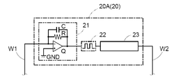
- the incident switching unit 20A may further include an amplifier 21 and a signal generator 22 indicated by a two-dot chain line as necessary.
- the amplifier 21 amplifies and outputs the electrical energy output from the photoelectric conversion element 30.
- the amplifier 21 may be provided when the liquid crystal shutter 23 cannot be directly driven by the electric energy output from the photoelectric conversion element 30.
- the electric energy is electric power, and includes the output current Iout shown in FIG. 4, the output voltage Vout shown in FIG. Unless explicitly stated, in this embodiment, the output voltage Vout is applied to electric energy.
- the amplifier 21 may be arbitrarily configured as long as it can amplify and output electrical energy.
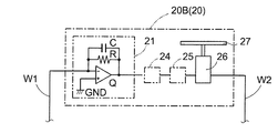
- the configuration example shown in FIG. 2 is an inverting amplifier including a capacitor C, a resistor R, and an operational amplifier Q.
- a capacitor C and a resistor R are connected in parallel to form a low-pass filter.
- the positive input (also referred to as non-inverting input) of the operational amplifier Q is connected to the ground GND, and the negative input is connected to the conductive wire W1.
- the capacitance of the capacitor C is 100 pF
- the resistance value of the resistor R is 10 M ⁇ .
- the signal generator 22 generates and outputs a switching signal for switching display / non-display of the liquid crystal shutter 23 based on the amplified output voltage Vout.
- the signal generator 22 may be prepared for a case where it is necessary to generate a switching signal by providing a time lag with the power signal in order to continue self-oscillation.
- the form of the switching signal may be arbitrarily set, and corresponds to, for example, a pulse signal or a data signal.
- the frequency for switching between display / non-display may be set arbitrarily, and may be adjusted to the frequency (for example, 50 Hz or 60 Hz) of the commercial power source.
- the liquid crystal shutter 23 transmits / not transmits light incident on the photoelectric conversion element 30 from the outside based on a signal output from the signal generator 22.
- the liquid crystal shutter 23 may be arbitrarily configured as long as light from the outside can be transmitted / non-transmitted. Although illustration is omitted, this embodiment does not include a light source, and includes a liquid crystal panel including a polarizing filter, a drive circuit for driving the liquid crystal panel, and the like. When light passes through the liquid crystal shutter 23, the light enters the photoelectric conversion element 30. On the other hand, if the light does not pass through the liquid crystal shutter 23, the light is not incident on the photoelectric conversion element 30.
- the light source that emits light is arbitrary, and may be natural light such as sunlight or artificial light such as an electric light. Regardless of whether the light is direct light or indirect light, any change over time, such as the amount of light or luminance, is not questioned. However, light that is continuously emitted including stationary light is targeted.
- the light may be incident from any direction as long as it can be excited by being incident on the photoelectric conversion element 30. For example, the incident direction indicated by arrow D1 in FIG. 1 is merely an example.
- the wavelength of light is arbitrary as long as an electromotive force is generated in the photoelectric conversion element 30. For example, it may be light having a plurality of wavelengths such as sunlight, or may be light having a single wavelength such as laser light or LED light.
- the photoelectric conversion element 30 includes a first electrode 31, a charge separation layer 32, an insulating polarization layer 33, a second electrode 34, and the like as shown in FIG.
- the first electrode 31 and the second electrode 34 correspond to “a pair of electrodes” and may be formed of any material having conductivity. Regardless of the difference in work function, it does not matter whether it is transparent or not. As described in the 5th edition of the RIKEN Dictionary (Iwanami Shoten, 1998), the work function is "necessary to extract one electron from the surface of a material (metal or semiconductor crystal, etc.) to the outside. It means “minimum energy”. When making a difference in work function between the first electrode 11 and the second electrode 15, charge separation in the charge separation layer 32 is increased.
- the first insulator 12 and the second insulator 14 also assist in charge separation. That is, since the polarization generated in the charge separation layer 32 is transmitted to the first electrode 11 and the second electrode to cause a transient potential difference between them, the responsiveness output after the charge separation layer 32 receives light ( High light-current conversion efficiency and short light-current conversion time) can be further increased than before.
- Transparent conductive materials include conductive metal oxides such as tin oxide (ATO, FTO) doped with antimony or fluorine, tin oxide, zinc oxide, indium oxide, indium tin oxide (ITO), indium zinc oxide (IZO), etc. This applies to things.
- a metal thin film such as gold, silver, chromium, or nickel may be used. It may be a mixture or laminate of a conductive metal oxide or metal thin film and a conductive metal oxide.
- An inorganic conductive material such as copper iodide or copper sulfide may be used.
- Organic conductive materials such as carbon nanotubes, polypyrrole, polyaniline, polythiophene, polypyrrole, and polyethylenedioxythiophene (PEDOT) may be used.
- a laminate formed by laminating one or more of metals, inorganic conductive materials, and organic conductive materials and indium tin oxide (ITO) may be used. From the viewpoint of high conductivity and transparency, a transparent conductive metal oxide is desirable.
- the charge separation layer 32 corresponds to a “charge separation portion”.
- the charge separation layer 32 may be formed of any material or shape as long as it is a compound that separates charges by receiving light, and whether or not it is a semiconductor (including p-type and n-type types). It doesn't matter. That is, any material may be used as long as holes and electrons move to the first electrode 31 when receiving charges to separate charges.
- the charge separation layer 32 may include one or more materials among organic compounds, inorganic compounds, and metal complexes on the condition that charge separation can be performed by receiving light.
- the thickness of the charge separation layer 32 may be set from the viewpoint of easily separating charges by receiving light and securing a desired electromotive force. This is because as the charge separation layer 32 becomes thinner, charge separation becomes easier, but the electromotive force also becomes smaller.
- a compound having a perovskite crystal structure may be used as a material example of the charge separation layer 32.
- a compound having a perovskite crystal structure is a ternary compound represented by the general formula ABX 3 such as barium titanate (BaTiO 3 ) or lead methylammonium iodide (CH 3 NH 3 PbI 3 ).
- A, B, and X correspond to metal ions, alkyl groups, amino groups, and the like.
- a perovskite structure is formed by a combination in which the valences of the A ion and the B ion are trivalent on average. In the case of an oxide in which X is oxygen, there are combinations such as A 2+ B 4+ O 3 , A 1+ B 5+ O 3 and A 3+ B 3+ O 3 .
- the charge separation layer 32 includes a donor or acceptor having an absorption band in a specific wavelength range included in incident light, a charge transfer complex having a charge transfer absorption band in a specific wavelength range (an intermolecular compound of a donor and an acceptor). Or a mixture of the donor and the acceptor. In other words, it is sufficient that charge separation occurs, and it may be formed using a donor or acceptor that excites an absorption band including a charge transfer absorption band.
- the donor here is an “electron-donating compound” corresponding to a compound that easily donates an electron
- the acceptor is an “electron-accepting compound” that corresponds to a compound that easily accepts an electron.
- the specific wavelength region When the specific wavelength region is a visible light wavelength region, it is formed of a charge transfer complex having a charge transfer absorption band in the visible light wavelength region or a mixture of its donor and acceptor. Similarly, when the specific wavelength region is an ultraviolet light wavelength region, it is formed of a donor or an acceptor having an absorption band in the ultraviolet light wavelength region, or a mixture of the donor and the acceptor.
- the combination of the donor and the acceptor is determined relatively from the energy level of the energy level of the compound to be combined, but any material may be applied.
- phthalocyanine (M-Pc) as a donor and fullerene compound as an acceptor are applicable.
- H 2 , TiO, VO, Mn, Fe, Co, Zn, Sn, Pb, Li, or the like can be applied to M coordinated at the center of phthalocyanine.
- Fullerene compounds include fullerene C 60 , fullerene C 70 , fullerene C 76 , fullerene C 78 , fullerene C 80 , fullerene C 82 , fullerene C 84 , fullerene C 90 , fullerene C 96 , fullerene C 240 , fullerene C 540 ,
- fullerene C 540 For example, mixed fullerene and fullerene nanotubes are applicable.
- the fullerene compound described above may include a fullerene derivative to which a substituent is added. Any group can be applied as the substituent. For example, halogen atom, alkyl group, alkenyl group, alkynyl group, aryl group, heterocyclic group, cyano group, hydroxyl group, nitro group, carboxyl group, alkoxy group, aryloxy group, silyloxy group, heterocyclic oxy group, acyloxy group , Carbamoyloxy group, alkoxycarbonyloxy group, aryloxycarbonyloxy group, amino group, ammonio group, acylamino group, aminocarbonylamino group, alkoxycarbonylamino group, aryloxycarbonylamino group, sulfamoylamino group, alkyl and aryl Sulfonylamino group, mercapto group, alkylthio group, arylthio group, heterocyclic thio group, s
- the mixture of donor and acceptor may be formed of a single component material.
- the single component substance include cyclic thiazyl radical (BDTDA) and N-ethylphenazyl.
- the specific wavelength region is a wavelength region of infrared light (preferably near infrared light)
- a charge transfer complex having a charge transfer absorption band in infrared light (or near infrared light) or a donor thereof And a mixture of acceptors.
- Any combination of donor and acceptor can be used as long as the above conditions are satisfied.
- a combination of tetrathiafulvalene (TTF) as a donor and chloranil (CA) as an acceptor is applicable.
- a combination of a cyclic dithiazole compound (NT) as a tetracyanoquinodimethane (TCNQ) as an acceptor is also applicable.
- the insulating polarization layer 33 corresponds to an “insulating polarization portion”.
- the insulating polarization layer 33 may be formed of any material (for example, an ionic liquid or a solid insulator) or a shape having both insulating properties and power storage properties. That is, the charge separation layer 32 has a function of promoting the separation of the charges and making the separated charges easy to be absorbed by the second electrode 34.
- the thickness of the insulating polarization layer 33 is preferably set from the viewpoint of securing a larger capacitance and facilitating polarization. This is because as the insulating polarization layer 33 becomes thicker, the capacitance decreases, the polarization also decreases, and the electromotive force decreases.
- the capacitance of the insulating polarization layer 33 may be set so that the alternating current (output current Iout described later) or the alternating voltage (output voltage Vout described later) becomes a target value (maximum value, amplitude value, etc.).
- the insulating polarization layer 33 can be formed of any material.
- an ionic liquid containing cation and anion as main components may be applied.
- Ionic liquids generally have a very low vapor pressure and are flame retardant or non-flammable. In many cases, the melting point is near room temperature, as sometimes called room temperature molten salt.
- the ionic liquid of this form should just be a liquid in a use temperature range.
- Cation is not particularly limited.
- nitrogen-containing compound power thione quaternary phosphonium cation, sulfonium cation and the like can be mentioned.
- nitrogen-containing compound power thione include heterocyclic aromatic cations such as imidazolium cation and pyridinium cation, piperidinium cation, pyrrolidinium cation, pyrazolium cation, thiazolium cation and morpholinium cation.
- heterocyclic cation such as a heterocyclic aliphatic cation, a quaternary ammonium cation, or a cation in which hydrogen is added to an aromatic amine, aliphatic amine, or alicyclic amine.
- the anion is not particularly limited.
- halide anions such as Cl ⁇ , Br ⁇ and I ⁇
- boron anions such as BF 4 ⁇ , B (CN) 4 ⁇ and B (C 2 O 4 ) 2 ⁇ , (CN) 2 N ⁇
- Amide anions and imide anions such as N (SO 2 F) 2 ] ⁇ , [N (SO 2 CF 3 ) 2 ] ⁇ , [N (SO 2 C 2 F 5 ) 2 ] ⁇ , RSO 3 ⁇ , RSO 4 ⁇ Sulfate anions such as RfSO 3 ⁇ and RfSO 4 ⁇ or sulfonate anions
- phosphate anions such as Rf 2 P (O) O ⁇ , PF 6 ⁇ and Rf 3 PF 3 ⁇
- antimony anions such as SbF 6 Is applicable.
- R is an “aliphatic hydrocarbon group or aromatic hydrocarbon group”, and Rf is a “fluorinated halogenated hydrocarbon group”.
- various anions such as lactate, nitrate ion, trifluoroacetate, and the like are applicable.
- the ionic liquid may be a combination of the above-described cation and anion, or may be a mixture of one or both of the cation and anion.
- an ionic liquid showing a gel or a plastic crystal phase may be used.
- a plastic crystal is also called a plastic crystal, and is a substance showing a flexible intermediate phase state while taking a crystal form, and exhibits relatively high ionic conductivity.
- Plastic crystals melt like normal crystals when heated to high temperatures. Unlike the crystalline state where ions are almost completely fixed, the plastic crystal phase has the advantage that ions can move freely to some extent. While maintaining the shape of a soft polymer at room temperature while having the non-combustible and non-volatile characteristics of ionic liquid, performance equivalent to ionic liquid can be obtained without leakage of ionic liquid.
- Solid insulators include, for example, polyvinylidene difluoride (PVDF), polyvinyl fluoride (PVF), polytetrafluoroethylene (PTFE), tetrafluoroethylene / ethylene copolymer (ETFE), and tetrafluoroethylene / hexafluoropropylene copolymer.
- PVDF polyvinylidene difluoride
- PVF polyvinyl fluoride
- PTFE polytetrafluoroethylene
- ETFE tetrafluoroethylene / ethylene copolymer
- tetrafluoroethylene / hexafluoropropylene copolymer tetrafluoroethylene / hexafluoropropylene copolymer
- Fluorine plastics such as polymer (FEP), tetrafluoroethylene / perfluoroalkyl / vinyl ether copolymer (PFA), polychloro / trifluoroethylene (PCTFE), chlorotrifluoroethylene / ethylene copolymer (ECTFE), etc. (Fluororesin) and the like are applicable. Note that a space (that is, a vacuum or quasi-vacuum space) in which charge transfer is extremely difficult may be formed without being limited to substances.
- the manufacturing method of the photoelectric conversion element 30 is arbitrary.
- the left first electrode 31 may be sequentially formed on the right side, and the right second electrode 34 may be sequentially formed on the left side.
- the charge separation layer 32 and the insulating polarization layer 33 may be integrally formed as an organic layer as a whole. If the first electrode 31 and the second electrode 34 are organic materials, the electrodes may be integrally formed together.
- the charge separation layer 32 and the insulating polarization layer 33 may be contacted after being formed separately.
- the change in electromotive force that is, rise and fall
- the switching between the incident state and the non-incident state in the incident switching unit 20 is steep.
- the steep time scale is better as soon as possible (that is, as the time required for change is short).
- the self-oscillation condition may be earlier than the time lag (that is, shorter in time).
- the predetermined time lag may be set to an appropriate numerical value in accordance with each type of light, the charge separation layer 32, the insulating polarization layer 33, the incident switching unit 20, and the like. For self-oscillation, it may be longer than the rise time and fall time. That is, the relationship of switching time ⁇ time lag may be satisfied.
- a time lag in which the incident switching unit 20 is switched to the non-incident state after the charge separation is performed in the charge separation layer 32 with the incidence of light and the electromotive force increases and the carriers are accumulated in the insulating polarization layer 33. .
- the alternating current or the alternating voltage can be self-oscillated and output from the first electrode 31 and the second electrode 34 which are output terminals, and can be sustained.
- the photoelectric conversion element 30 that obtained the characteristic lines shown in FIGS. 4 and 5 was configured as follows. Indium oxide (ITO / PEDOT: PSS) was used for the first electrode 31. For the charge separation layer 32, lead methylammonium iodide (CH 3 NH 3 PbI 3 ) having a perovskite crystal structure was used. N, N-diethyl-N-methyl-N- (2-methoxyethyl) ammonium tetrafluoroborate (DEME-BF 4 ), which is one of ionic liquids, was used for the insulating polarization layer 33. Aluminum (Al) was used for the second electrode 34. Light was incident from the ITO side, and ITO became the cathode. This configuration is merely an example, and the same results as those described below were obtained even when the materials used for the above-described elements were arbitrarily combined.
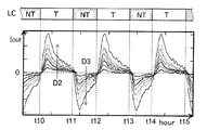
- the output current Iout shown in FIG. 4 is a result of measurement by connecting an ammeter between the conductive wire W1 and the conductive wire W2.
- “LC” shown in the upper part is the operation of the liquid crystal shutter 23.
- “T” is shown in the sense that light is transmitted through the liquid crystal shutter 23 and incident on the photoelectric conversion element 30, and the light does not pass through the liquid crystal shutter 23 and enters the photoelectric conversion element 30.
- a non-incident state where light is not incident is illustrated as “NT” in the meaning of non-transmission.
- Non-transparency is indicated by hatching lines for easy distinction. That is, light is transmitted from time t10 to time t11, from time t12 to time t13, and from time t14 to time t15. Light does not transmit from time t11 to time t12 and from time t13 to time t14.
- the output current Iout changes in the positive direction when light is incident, and changes in the negative direction when no light is incident. That is, when light is incident on the charge separation layer 32, the energy is excited and charge separation is performed, and the charge separation layer 32 is separated into holes and electrons, and polarization is generated in this. This polarization polarizes the insulating polarization layer 33. This polarization is transmitted to the conducting wires W1 and W2, and a positive output current Iout flows. When the light is not incident on the charge separation layer 32, the polarization is eliminated. Therefore, an output current Iout in the opposite direction, that is, in the negative direction, flows through the conductive wires W1 and W2. Therefore, the output current Iout becomes an alternating current. Depending on the configuration of the charge separation layer 32, the amplitude changes as indicated by arrows D2 and D3.
- the output voltage Vout shown in FIG. 5 is a result of measurement by connecting a voltmeter between the conducting wire W1 and the conducting wire W2.
- “LC” shown in the upper part is the same as FIG. Therefore, light is transmitted from time t20 to time t21, from time t22 to time t23, and from time t24 to time t25. Light is not transmitted from time t21 to time t22 and from time t23 to time t24. Since the output voltage Vout changes according to charge separation and polarization in the same manner as the output current Iout in FIG. 4, it becomes an AC voltage. Depending on the configuration of the charge separation layer 32, the amplitude changes as indicated by arrows D4 and D5.
- 4 and 5 show examples in which the transmission period during which light is transmitted is different from the non-transmission period during which light is not transmitted.
- the display / non-display of the liquid crystal shutter 23 can be switched so that the transmission period and the non-transmission period are the same.
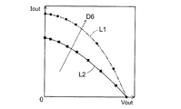
- FIG. 6 shows the characteristics when the AC frequency is changed when the vertical axis is the output current Iout and the horizontal axis is the output voltage Vout.
- the AC frequency is 400 Hz, it changes like the characteristic line L1
- the AC frequency is 50 Hz, it changes like the characteristic line L2.
- the output current Iout increases as the AC frequency increases. In other words, the frequency may be increased if a large current is required.
- the liquid crystal shutter 23 shown in FIG. 2 outputs an output current Iout and an output voltage Vout for one cycle when transmission and non-transmission are switched based on a signal transmitted from the signal generator 22. Therefore, in order to set the characteristic line L1 shown in FIG. 6 to 400 Hz, the signal generator 22 may output a signal that alternately repeats transmission and non-transmission 400 times. Similarly, in order to set the characteristic line L2 to 50 Hz, it is preferable to output a signal that alternately repeats transmission and non-transmission 50 times. That is, the output current Iout and the output voltage Vout can be output at the target frequency by appropriately setting or controlling the signal generated by the signal generator 22.
- the photoelectric conversion device 10B shown in FIGS. 7 to 9 is an example of the photoelectric conversion device 10.
- the photoelectric conversion device 10B includes an incident switching unit 20B, a photoelectric conversion element 30, and the like.
- the photoelectric conversion device 10B is different from the photoelectric conversion device 10A in that an incident switching unit 20B is used instead of the incident switching unit 20A.
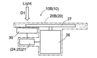
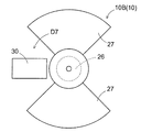
- the incident switching unit 20B corresponding to the “movement mechanism” includes an amplifier 21, a motor 26, an opaque member 27, and the like.
- the rectifier 24 and the inverter 25 shown in FIG. 9 may be included.
- the motor 26 rotates the opaque member 27 in accordance with the signal output from the amplifier 21.
- the opaque member 27 is fixed to the rotating shaft of the motor 26 so as to pass between the light source and the photoelectric conversion element 30.
- Any form of the opaque member 27 (for example, material, shape, number, etc.) can be used as long as it can block light.
- the shape of the opaque member 27 is arbitrary as long as it is a shape that alternately switches between an incident state in which light is transmitted with rotation and a non-incident state in which light is not transmitted.
- the rotation direction may be a left rotation illustrated in the direction of arrow D7 or a right rotation (not illustrated).
- FIG. 8 shows an example in which two opaque members 27 are formed in a fan shape with a central angle of 90 degrees. Although not shown, it may be formed in a shape other than a fan shape.
- the central angle may be arbitrarily set as long as a non-incident state in which light does not enter the charge separation layer 32 can be secured.
- a rectifier 24 may be provided, and an inverter 25 may be further provided.
- the rectifier 24 may include an element capable of outputting a constant voltage (eg, a Zener diode), a constant voltage circuit, an element capable of outputting a constant current (eg, a constant current diode), and a constant current circuit.
- a constant voltage eg, a Zener diode
- a constant current eg, a constant current diode
- the motor 26 is a direct current motor, it can be driven by rectifying the alternating current output from the photoelectric conversion element 30 by the rectifier 24 and converting it to direct current.
- the motor 26 is an AC motor, it can be driven if the AC output from the photoelectric conversion element 30 is rectified by the rectifier 24 and converted to DC, and further converted by the inverter 25 to AC.
- the opaque member 27 shown in the configuration example of FIG. 8 switches the incident state and the non-incident state twice each time it rotates, so that it outputs an output current Iout and an output voltage Vout of two cycles. Therefore, in order to obtain 400 Hz of the characteristic line L1 shown in FIG. Similarly, in order to set the characteristic line L2 to 50 Hz, it is preferable to rotate at 25 rpm. That is, by appropriately setting or controlling the rotation of the motor 26, the output current Iout and the output voltage Vout can be output at the target frequency.
- the opaque member 27 of the incident switching unit 20B in the second embodiment described above is composed of two opaque members 27 formed in a fan shape with a central angle of 90 degrees (see FIG. 8). Instead of this form, a plurality of opaque members 27 formed into a predetermined shape at a central angle other than 90 degrees may be used.
- the predetermined shape may be a fan shape or a geometric shape such as a triangle or a quadrangle.
- three opaque members 27 formed with a central angle of 60 degrees, four opaque members 27 formed with a central angle of 45 degrees, and the like are applicable.
- a moving mechanism including a member that transmits / non-transmits light other than the opaque member 27 may be applied. In any case, the same effects as those of the second embodiment can be obtained.
- the liquid crystal shutter 23 of the first embodiment described above is configured to switch between the incident state and the non-incident state on the entire surface, and the opaque member 27 of the second embodiment is configured to be formed into a fan shape (see FIGS. 1 and 8). ).
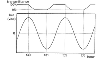
- the waveform is as shown in FIG. 4 and FIG. 5, which is a waveform different from a sine wave (which may be a cosine wave; the same applies hereinafter).
- the liquid crystal shutter 23 may be configured to control the display so that the incident state and the non-incident state on the charge separation layer 32 are partially switched. You may comprise in the shape from which a non-incident state switches partially.
- Partially switching means that the transmittance of light passing through the liquid crystal shutter 23 and the opaque member 27 and entering the charge separation layer 32 is sequentially increased from 0% to 100%, and the transmittance is also increased from 0% to 100%. It is a control or shape that increases sequentially to%.
- the output current Iout and the output voltage Vout output from the first electrode 31 and the second electrode 34 that are output terminals can be sine waves as shown in FIG.
- the control and shape can be set so as to have a waveform other than a sine wave (for example, a rectangular wave, a triangular wave, a sawtooth wave, etc.). According to this configuration, the output current Iout and the output voltage Vout can be output in a target waveform, and the same effect as in the first and second embodiments can be obtained.
- the insulating polarization layer 33 included in the photoelectric conversion element 30 is formed of an ionic liquid having a certain capacity (see FIG. 3).
- it may be configured to have a liquid increase / decrease control unit for increasing / decreasing the capacity of the ionic liquid contained in the insulating polarization layer 33.
- the insulating polarization layer 33 includes an insulating container and a liquid increase / decrease control unit that increases or decreases the capacity of the ionic liquid relative to the container.
- the output current Iout and the output voltage Vout can be controlled to predetermined target values by controlling the volume of the ionic liquid contained in the container.
- the liquid crystal shutter 23 of the incident switching unit 20A and the photoelectric conversion element 30 are configured separately (see FIG. 3).
- the liquid crystal shutter 23 and the photoelectric conversion element 30 may be integrally formed by sharing the electrode of the liquid crystal shutter 23 and the electrode of the photoelectric conversion element 30.
- the shared electrode has the same potential. Therefore, when the driving voltage of the liquid crystal shutter 23 and the electromotive force of the photoelectric conversion element 30 are different, it is desirable to use the shared electrode as the ground GND. According to this configuration, the integrated photoelectric conversion device 10 is obtained, and the size and size can be reduced, and the same effect as that of the first embodiment can be obtained.
- a pair of electrodes including the first electrode 31 and the second electrode 34 serving as output terminals and the first electrode 31 are provided so as to receive light.
- An incident switching unit 20 (20A, 20B) that alternately switches between a non-incident state and a non-incident state, charge separation by the charge separation layer 32, storage and discharge by the insulating polarization layer 33, and incidence state by the incident switching unit 20.
- Self-oscillates depending on the non-incident state Configured to output sustained an alternating current or alternating voltage from the output terminal (1, 7, see Figure 8).
- the incident switching unit 20 switches between an incident state and a non-incident state alternately. These combine to self-oscillate, and an alternating current or alternating voltage is continuously output from the output terminals (that is, the first electrode 31 and the second electrode 34). Furthermore, since the incident switching unit 20 switches alternately between the incident state and the non-incident state based on the current flowing between the first electrode 31 and the second electrode 34, the electrical energy output from the output terminal is changed to alternating current. Can do.
- a predetermined time lag is provided between a change in electromotive force and switching between an incident state and a non-incident state in the incident switching unit. According to this configuration, it is possible to reliably oscillate and sustain the output of an alternating current or alternating voltage from the output terminal.
- the charge separation layer 32 is configured to include one or more of an organic compound, an inorganic compound, and a metal complex that can receive light and perform charge separation. According to this configuration, the charge separation unit can be configured with a material that can reliably generate power.
- the charge separation layer 32 is configured to include one or both of a donor and an acceptor having a charge transfer absorption band. According to this configuration, the charge separation layer 32 can be formed of a material corresponding to the wavelength range of incident light.
- the charge separation layer 32 includes a compound having a perovskite crystal structure. According to this configuration, power generation can be performed at low cost and high efficiency, and the output current Iout (alternating current) and the output voltage Vout (alternating voltage) can be increased.
- the insulating polarization layer 33 is configured to be an ionic liquid containing cation and anion as main components. According to this configuration, since the electric double layer is formed at the interface with the charge separation layer 32, the generation of carriers is promoted and a large amount of power generation can be obtained.
- the ionic liquid is configured to exhibit a plastic crystal phase. According to this configuration, free movement of ions contained in the ionic liquid can be ensured, and leakage from the photoelectric conversion element 30 to the outside can be prevented.
- the incident switching unit 20 covers at least the photoelectric conversion element 30 (that is, the charge separation layer 32), and the liquid crystal shutter 23 capable of alternately changing light transmission and blocking over time, or the light source and the photoelectric conversion element 30
- the opaque member 27 is moved so as to pass between the two, so that the transmission and blocking of light can be alternately changed (see FIGS. 1, 7, and 8). According to this configuration, since the incident state and the non-incident state are switched alternately, the electric energy output from the output terminals (the first electrode 31 and the second electrode 34) can be reliably maintained.
- the present invention it is possible to provide a photoelectric conversion device capable of sustaining the self-oscillation of conversion from light energy to AC electrical energy.
Landscapes
- Engineering & Computer Science (AREA)
- Chemical & Material Sciences (AREA)
- Power Engineering (AREA)
- Materials Engineering (AREA)
- Chemical Kinetics & Catalysis (AREA)
- Electrochemistry (AREA)
- Microelectronics & Electronic Packaging (AREA)
- Physics & Mathematics (AREA)
- Electromagnetism (AREA)
- General Chemical & Material Sciences (AREA)
- Photovoltaic Devices (AREA)
- Electroluminescent Light Sources (AREA)
Abstract
光エネルギーを交流の電気エネルギーに変換して出力する光電変換装置を提供することである。光電変換装置10は、第1電極31と第2電極34とを含む一対の電極と、第1電極31に接触して設けられる電荷分離層32(電荷分離部)と、電荷分離層32と第2電極34との間に介在されて設けられる絶縁分極層33(絶縁分極部)と、第1電極31と第2電極34との間を流れる電流に基づいて、光が電荷分離層32に入射する入射状態と、光が電荷分離層32に入射しない非入射状態とを交互に切り替える入射切替部20とを有し、電荷分離層32による電荷分離と、絶縁分極層33による蓄電および放電と、入射切替部20による入射状態と非入射状態の切り替えとによって自己発振し、出力端子から交流電流または交流電圧を持続して出力する。この構成によれば、自己発振により交流を出力し、かつ持続できる。
Description
本発明は、光エネルギーを電気エネルギーに変換して出力する光電変換装置に関する。
有機物を利用して光エネルギーを電気エネルギーに変換する太陽電池として、無機系の太陽電池と同様にpn接合からの電荷分離を起点とする有機薄膜太陽電池と、酸化チタン表面の吸着色素からの電荷分離を起点とする色素増感太陽電池が知られている。
有機薄膜太陽電池や色素増感太陽電池では、直流電流が常にデバイス内を流れ続けるため、移動度の低い有機物にとって、本質的に不利な構造であると言わざるを得ない。また上記エネルギー変換では必ず直流電流が出力され、交流電流は出力されない。
従来では、安価に作製でき、暗電流の発生が極力抑えられ、光を受けて大きくかつ高速の応答性をもつ過渡電流を発生させることを目的とする有機光電変換素子に関する技術の一例が開示されている(例えば特許文献1を参照)。この有機光電変換素子は、仕事関数に差をつけた第1電極および第2電極と、光を受けて電荷を分離する電荷分離層と、電極と電荷分離層とを絶縁して分極する絶縁分極層とを有する。電荷分離層と絶縁分極層を組み合わせることで、大きな過渡電流を取り出すことができる。
しかし、特許文献1に記載の有機光電変換素子は、チョップ光のような断続的な光が入射されることを条件として、交流電流を出力する。すなわち、単に光を入射させただけでは交流電流を出力することができない。よって、交流電流が必要とされる場合には、外部電源を利用して光チョッパーなどを駆動して光を変調する必要があるという問題点があった。
本開示はこのような点に鑑みてなしたものであり、光エネルギーから交流の電気エネルギーへの変換を自己発振して持続できる光電変換装置を提供することを目的とする。
上記課題を解決するためになされた第1の発明は、光エネルギーを電気エネルギーに変換して出力する光電変換装置において、出力端子となる第1電極と第2電極とを含む一対の電極と、前記第1電極に接触して設けられ、光を受けて電荷分離する電荷分離部と、前記電荷分離部と前記第2電極との間に介在されて設けられ、前記第1電極と前記電荷分離部とを絶縁して分極する絶縁分極部と、前記第1電極と前記第2電極との間に生じる起電力に基づいて、光が前記電荷分離部に入射する入射状態と、光が前記電荷分離部に入射しない非入射状態とを交互に切り替える入射切替部とを有し、前記電荷分離部による電荷分離と、前記絶縁分極部による蓄電および放電と、前記入射切替部による前記入射状態と前記非入射状態の切り替えとによって自己発振し、前記出力端子から交流電流または交流電圧を持続して出力することを特徴とする。
この構成によれば、入射状態では電荷分離部で電荷分離したキャリア(すなわち正孔や電子)が絶縁分極部に蓄積して充電されるため、一方側電極(例えば第1電極)から他方側電極(例えば第2電極)に向かって電流が流れる。非入射状態では絶縁分極部に蓄積されたキャリアが放電されるため、他方側電極から一方側電極に向かって電流が流れる。すなわち、入射状態と非入射状態とでは電流の流れる方向が逆になる。入射切替部は入射状態と非入射状態とを交互に切り替える。これらが組み合わさって自己発振し、出力端子(すなわち第1電極および第2電極)からは交流電流または交流電圧が持続して出力される。さらに、入射切替部は第1電極と第2電極との間を流れる電流に基づいて入射状態と非入射状態とを交互に切り替えるので、出力端子から出力する電気エネルギーを交流にすることができる。
第2の発明は、前記起電力の変化と、前記入射切替部における前記入射状態と前記非入射状態の切り替えとの間に所定のタイムラグを設けることを特徴とする。この構成によれば、入射状態で起電力が大きくなって絶縁分極部にキャリアを蓄積してから非入射状態に切り替えたり、非入射状態で絶縁分極部に蓄積されたキャリアが放電されてから入射状態に切り替えたりする。充電のために入射状態から非入射状態への切り替えにタイムラグが必要となり、放電のために非入射状態から入射状態への切り替えにもタイムラグが必要となる。所定のタイムラグは、短すぎても自己発振せず、長すぎても自己発振しないので、光,電荷分離部,絶縁分極部および入射切替部などの条件に応じて適切な数値を設定するとよい。所定のタイムラグを適切に設定することによって、出力端子から交流電流または交流電圧の出力を確実に自己発振させ、かつ持続させることができる。
第3の発明は、前記電荷分離部は、光を受けて電荷分離が行える有機化合物,無機化合物,金属錯体のうちで一以上を含むことを特徴とする。この構成によれば、確実に発電を行える材料で電荷分離部を構成することができる。
第4の発明は、前記電荷分離部は、電荷移動吸収帯をもつドナーおよびアクセプターのうちで一方または双方を含むことを特徴とする。この構成によれば、入射される光の波長域に応じた材料で電荷分離部を構成することができる。
第5の発明は、前記電荷分離部は、ペロブスカイト型結晶構造の化合物を含むことを特徴とする。この構成によれば、低コストかつ高効率で発電が行え、交流電流や交流電圧を高めることができる。
第6の発明は、前記絶縁分極部は、陽イオンと陰イオンとを主成分として含むイオン液体であることを特徴とする。この構成によれば、電荷分離部との界面に電気二重層が形成されることで、電荷分離が促進され、大きな発電容量が得られる。
第7の発明は、前記イオン液体は、プラスチッククリスタル相を示すことを特徴とする。この構成によれば、イオン液体に含まれるイオンの自由な運動を確保することができ、光電変換素子から外部に漏洩するのを防止することができる。
第8の発明は、前記入射切替部は、少なくとも前記電荷分離部を覆って経時的に光の透過と遮断を交互に変えられる液晶シャッター、または、前記光源と前記電荷分離部との間を通過するように不透明部材を移動させて光の透過と遮断を交互に変えられる移動機構であることを特徴とする。この構成によれば、確実に入射状態と非入射状態とを交互に切り替えるので、出力端子から出力する電気エネルギーを確実に持続させることができる。
ここで、第1電極と第2電極との間に接続される導線を流れる「電流」は、主に過渡電流である。「電荷分離部」は、光を受けて電荷を分離できる材料で成形されていれば任意であり、ペロブスカイト型結晶構造の化合物を含む。「絶縁分極部」は、導電性よりも誘電性が優位な物質で形成されていれば任意であり、陽イオンと陰イオンとを主成分として含むイオン液体(Ionic Liquid)を含む。「イオン液体」は、陽イオンと陰イオンとを主成分として含む限りにおいて、液体でもよく、ゲル状でもよい。一対の電極(すなわち第1電極および第2電極)は、交流電源のように双方ともに極性が変換する電極として用いる。「接触」は接合を含み、接触面で一方から他方へ分極が伝わる形態を意味する。「透過」には反射を含む。
以下、本発明を実施するための形態について、図面に基づいて説明する。なお、特に明示しない限り、「接続する」という場合には電気的に接続することを意味する。各図は、本発明を説明するために必要な要素を図示し、実際の全要素を図示しているとは限らない。上下左右等の方向を言う場合には、図面の記載を基準とする。
〔実施の形態1〕
実施の形態1は図1~図6を参照しながら説明する。図1に示す光電変換装置10Aは、光電変換装置10の一例である。この光電変換装置10Aは、入射切替部20Aや光電変換素子30などを有する。
実施の形態1は図1~図6を参照しながら説明する。図1に示す光電変換装置10Aは、光電変換装置10の一例である。この光電変換装置10Aは、入射切替部20Aや光電変換素子30などを有する。
入射切替部20Aと光電変換素子30とは、導線W1,W2によって接続される。導線W1,W2のうちで一方は、グラウンドGNDに接続するとよい。グラウンドGNDは共通電位であり、必ずしも0[V]とは限らない。接地されたグラウンドGNDは0ボルトになる。後述するように出力電圧Voutや出力電流Ioutは交流であるので、図1に示すように導線W2をグラウンドGNDに接続してもよく、図示を省略するが導線W1をグラウンドGNDに接続してもよい。
入射切替部20Aは、入射切替部20の一例である。図2に一点鎖線で示す入射切替部20Aは、少なくとも液晶シャッター23などを有する。入射切替部20Aは、さらに二点鎖線で示す増幅器21や信号生成器22などを必要に応じて備えてもよい。
増幅器21は、光電変換素子30から出力される電気エネルギーを増幅して出力する。この増幅器21は、光電変換素子30から出力される電気エネルギーによって液晶シャッター23を直接駆動できない場合に備えるとよい。電気エネルギーは電力であり、図4に示す出力電流Ioutや、図5に示す出力電圧Voutなどを含む。明示しない限り、本形態では電気エネルギーに出力電圧Voutを適用する。
増幅器21は、電気エネルギーを増幅して出力できれば任意に構成してよい。図2に示す構成例は、コンデンサC,抵抗器R,オペアンプQを含む反転増幅器である。発振を防いで位相補償を行うために、コンデンサCと抵抗器Rを並列接続してローパスフィルタにする。当該並列接続の両端をオペアンプQのマイナス入力(反転入力とも呼ぶ)と出力とに接続することで、負帰還フィードバックを行う。オペアンプQのプラス入力(非反転入力とも呼ぶ)はグラウンドGNDに接続し、マイナス入力は導線W1に接続する。本形態では、コンデンサCの静電容量を100pFとし、抵抗器Rの抵抗値を10MΩとする。
信号生成器22は、増幅された出力電圧Voutに基づいて液晶シャッター23の表示/非表示を切り替える切替信号を生成して出力する。光電変換素子30から出力される電気エネルギーを電力信号と仮定するとき、信号生成器22は自己発振を継続するために電力信号とタイムラグを設けて切替信号を生成する必要がある場合に備えるとよい。当該切替信号の形態は任意に設定してよく、例えばパルス信号やデータ信号などが該当する。表示/非表示を切り替える周波数は任意に設定してよく、商用電源の周波数(例えば50Hzや60Hzなど)に合わせてもよい。液晶シャッター23は、信号生成器22から出力される信号に基づいて、外部から光電変換素子30に向けて入射される光を透過/非透過する。
液晶シャッター23は、外部からの光を透過/非透過できれば任意に構成してよい。図示を省略するが、本形態では光源を含まず、偏光フィルタを含む液晶パネルや、当該液晶パネルを駆動する駆動回路などを有する。光が液晶シャッター23を透過すると、光電変換素子30に入射される入射状態になる。これに対して、光が液晶シャッター23を透過しないと、光電変換素子30に入射されない非入射状態になる。
光を発する光源は任意であり、太陽光などの自然光でもよく、電灯などの人工光でもよい。光は、直接光や間接光を問わず、光量や輝度等の経時的変化は問わない。ただし、定常光を含めて連続的に発する光を対象とする。光は、光電変換素子30に入射して励起できれば、どの方向から入射してもよい。例えば、図1に矢印D1で示す入射方向は一例に過ぎない。光の波長は、光電変換素子30で起電力を生じれば任意である。例えば、太陽光のように複数の波長からなる光でもよく、レーザ光やLED光のように単一の波長からなる光でもよい。
光電変換素子30は、図3に示すように、第1電極31,電荷分離層32,絶縁分極層33,第2電極34などを有する。第1電極31および第2電極34は「一対の電極」に相当し、導電性を有する任意の材料で成形してよい。仕事関数の差を問わず、透明であるか否かを問わない。仕事関数は、理化学辞典第5版(岩波書店,1998年)にも記載されているように、「物質(金属や半導体の結晶等)表面からその外側へ1個の電子を取り出すのに必要な最小のエネルギー」を意味する。第1電極11と第2電極15との間で仕事関数に差をつける場合には、電荷分離層32内での電荷分離を増長する。第1絶縁体12や第2絶縁体14も電荷分離を助ける。すなわち、電荷分離層32内に生じた分極を第1電極11および第2電極に伝えて両者に過渡的な電位差を生じさせるので、電荷分離層32が光を受けてから出力される応答性(高い光-電流変換効率および短い光-電流変換時間)を従来よりもさらに高めることができる。
電極越しに電荷分離層32を励起する場合は、電極を透明にする必要がある。透明性導電材料は、例えばアンチモンやフッ素等をドープした酸化スズ(ATO,FTO)、酸化スズ、酸化亜鉛、酸化インジウム、酸化インジウムスズ(ITO)、酸化亜鉛インジウム(IZO)等の導電性金属酸化物などが該当する。金,銀,クロム,ニッケルなどの金属薄膜でもよい。導電性金属酸化物または金属薄膜と、導電性金属酸化物との混合物または積層物でもよい。ヨウ化銅や硫化銅などの無機導電性物質でもよい。カーボンナノチューブ,ポリピロール,ポリアニリン,ポリチオフェン,ポリピロール,ポリエチレンジオキシチオフェン(PEDOT)などの有機導電性材料でもよい。金属,無機導電性物質,有機導電性材料のうちで一以上と、酸化インジウムスズ(ITO)とを積層して成形した積層物でもよい。高導電性や透明性等の観点から、透明導電性金属酸化物が望ましい。
電荷分離層32は「電荷分離部」に相当する。この電荷分離層32は、光を受けて電荷を分離する化合物であれば任意の材料や形状で形成してよく、半導体(p型やn型等の型式を含めて)であるか否かを問わない。すなわち、光を受けて電荷を分離するにあたって、正孔や電子が第1電極31まで移動する材料であればよい。電荷分離層32は、光を受けて電荷分離が行えることを条件として、有機化合物,無機化合物,金属錯体のうちで一以上の材料を含めてよい。電荷分離層32の厚みは、光を受けて電荷分離させ易く、所望の起電力を確保する観点で設定するとよい。電荷分離層32が薄くなるにつれて電荷分離し易くなる反面、起電力も小さくなるためである。
電荷分離層32の材料例として、例えばペロブスカイト型結晶構造の化合物でもよい。具体的には、チタン酸バリウム(BaTiO3)やヨウ化鉛メチルアンモニウム(CH3NH3PbI3)などのように、一般式ABX3で示される3元系からなる化合物である。A,B,Xは、金属イオン、アルキル基、アミノ基などが該当する。AイオンとBイオンの原子価は足して平均で3価になるような組み合わせでペロブスカイト構造が成立する。Xが酸素となる酸化物の場合は、例えばA2+B4+O3、A1+B5+O3、A3+B3+O3などの組み合わせがある。
電荷分離層32は、入射された光に含まれる特定の波長域に吸収帯をもつドナーまたはアクセプター、特定の波長域に電荷移動吸収帯をもつ電荷移動錯体(ドナーとアクセプターとの分子間化合物)、あるいはそのドナーとアクセプターとの混合物などでもよい。すなわち電荷分離さえ起こればよく、電荷移動吸収帯を含めた吸収帯を励起するドナーやアクセプターを用いて形成すればよい。ここにいうドナーは電子を供与しやすい化合物に相当する「電子供与性化合物」であり、同様にアクセプターは電子を受容しやすい化合物に相当する「電子受容性化合物」である。
特定の波長域が可視光の波長域である場合には、可視光の波長域に電荷移動吸収帯をもつ電荷移動錯体、あるいはそのドナーとアクセプターの混合物で形成する。同様に特定の波長域が紫外光の波長域である場合には、紫外光の波長域に吸収帯をもつドナーまたはアクセプター、あるいはそのドナーとアクセプターとの混合物で形成する。
ドナーとアクセプターの組み合わせは、組み合わせの対象となる化合物のエネルギー準位のエネルギーレベルから相対的に決定されるものの、任意の材料を適用してよい。例えば、ドナーとしてのフタロシアニン(M-Pc)と、アクセプターとしてのフラーレン化合物とが該当する。フタロシアニンの中央部に配位されるMには、H2,TiO,VO,Mn,Fe,Co,Zn,Sn,Pb,Liなどを適用できる。フラーレン化合物は、フラーレンC60のほか、フラーレンC70、フラーレンC76、フラーレンC78、フラーレンC80、フラーレンC82、フラーレンC84、フラーレンC90、フラーレンC96、フラーレンC240、フラーレンC540、ミックスドフラーレン、フラーレンナノチューブなどが該当する。
上述したフラーレン化合物には、置換基が付加されたフラーレン誘導体を含めてよい。当該置換基としては任意の基を適用できる。例えば、ハロゲン原子、アルキル基、アルケニル基、アルキニル基、アリール基、複素環基、シアノ基、ヒドロキシル基、ニトロ基、カルボキシル基、アルコキシ基、アリールオキシ基、シリルオキシ基、ヘテロ環オキシ基、アシルオキシ基、カルバモイルオキシ基、アルコキシカルボニルオキシ基、アリールオキシカルボニルオキシ基、アミノ基、アンモニオ基、アシルアミノ基、アミノカルボニルアミノ基、アルコキシカルボニルアミノ基、アリールオキシカルボニルアミノ基、スルファモイルアミノ基、アルキル及びアリールスルホニルアミノ基、メルカプト基、アルキルチオ基、アリールチオ基、ヘテロ環チオ基、スルファモイル基、スルホ基、アルキル及びアリールスルフィニル基、アルキル及びアリールスルホニル基、アシル基、アリールオキシカルボニル基、アルコキシカルボニル基、カルバモイル基、アリール及びヘテロ環アゾ基、イミド基、ホスフィノ基、ホスフィニル基、ホスフィニルオキシ基、ホスフィニルアミノ基、ホスホノ基、シリル基、ヒドラジノ基、ウレイド基、ボロン酸基、ホスファト基、スルファト基などが該当する。
上述したドナーとアクセプターの混合物以外では、単成分物質で形成してもよい。単成分物質は、例えば環状チアジルラジカル(BDTDA)のほか、N-エチルフェナジルなどが該当する。
上記特定の波長域が赤外光(望ましくは近赤外光)の波長域である場合には、赤外光(もしくは近赤外光)に電荷移動吸収帯をもつ電荷移動錯体、あるいはそのドナーとアクセプターの混合物で形成する。ドナーとアクセプターの組み合わせは、上記条件を満たせば任意の物質を適用することができる。例えば、ドナーとしてのテトラチアフルバレン(TTF)と、アクセプターとしてのクロラニル(CA)との組み合わせが該当する。また、としての環状ジチアゾール化合物(NT)と、アクセプターとしてのテトラシアノキノジメタン(TCNQ)との組み合わせも該当する。
絶縁分極層33は「絶縁分極部」に相当する。この絶縁分極層33は、絶縁性と蓄電性とを兼ね備える任意の材料(例えばイオン液体や固体絶縁体など)や形状で形成してよい。すなわち、電荷分離層32における電荷の分離を促進し、分離した電荷が第2電極34に吸収し易くする機能を担う。絶縁分極層33の厚みは、より大きな静電容量を確保し、分極させ易くする観点で設定するとよい。絶縁分極層33が厚くなるにつれて静電容量が減少し、分極も減少して起電力が小さくなるためである。交流電流(後述する出力電流Iout)または交流電圧(後述する出力電圧Vout)が目的値(最大値や振幅値など)となるように、絶縁分極層33の静電容量を設定するとよい。
絶縁分極層33は任意の物質で形成することが可能である。例えば陽イオンと陰イオンとを主成分として含むイオン液体を適用してもよい。イオン液体は、一般的に、極めて低い蒸気圧を有し、難燃性もしくは不燃性を有する。常温溶融塩と称されることもあるように、融点が室温付近にあるものが多い。本形態のイオン液体は、使用温度範囲で液体であればよい。
陽イオンは特に限定されるものではない。例えば、窒素含有化合物力チオン、第四級ホスホニウムカチオン、スルホニウムカチオン等が挙げられる。窒素含有化合物力チオンとしては、例えば、イミダゾリウムカチオン、ピリジニウムカチオン等の複素環式芳香族系カチオン、ピペリジニウムカチオン、ピロリジニウムカチオン、ピラゾリウムカチオン、チアゾリウムカチオン、モルフォリニウムカチオン等の複素環式脂肪族系カチオン、第四級アンモニウムカチオン、もしくは芳香族アミン、脂肪族アミン、脂環式アミンに水素が付加した形のカチオン等が該当する。
陰イオンは特に限定されるものではない。例えば、Cl-、Br-、I-などのハロゲン化物アニオン、BF4
-、B(CN)4
-、B(C2O4)2
-等のホウ素化物アニオン、(CN)2N-、[N(SO2F)2]-、[N(SO2CF3)2]-、[N(SO2C2F5)2]-等のアミドアニオンやイミドアニオン、RSO3
-、RSO4
-、RfSO3
-、RfSO4
-等のスルフェートアニオン又はスルフォネートアニオン、Rf2P(O)O-、PF6
-、Rf3PF3
-等のリン酸アニオン、SbF6等のアンチモンアニオンなどが該当する。なお、Rは「脂肪族炭化水素基又は芳香族炭化水素基」とし、Rfは「含フッ素ハロゲン化炭化水素基」とする。その他、ラクテート、硝酸イオン、トリフルオロアセテート等、各種の陰イオンなどが該当する。
イオン液体は、上述したカチオン及びアニオン1種ずつの組み合わせからなるものでもよく、カチオン及びアニオンについて片方もしくは両方が2種以上混在するものからなるものでもよい。
またイオン液体には、ゲルやプラスチッククリスタル相(柔粘性結晶相)を示すイオン液体を用いてもよい。プラスチッククリスタルは柔粘性結晶とも呼ばれ、結晶形態をとりながら柔軟性を有する中間相状態を示す物質であり、比較的高いイオン伝導性を示す。プラスチッククリスタルは高温にすると、通常の結晶と同様に融解する。イオンがほぼ完全に固定されてしまう結晶状態と異なり、プラスチッククリスタル相の中では、イオンがある程度自由に運動できる利点がある。イオン液体の不燃性不揮発性の特性を有しながら、室温で軟質のポリマーのような形状を維持する為、イオン液体が漏洩することなくイオン液体同等の性能を得ることができる。
上述したイオン液体に代えて、固体絶縁体を用いてもよい。固体絶縁体は、例えばポリビニリデンジフルオライド(PVDF)、ポリビニルフルオライド(PVF)、ポリテトラフルオロエチレン(PTFE)、テトラフルオロエチレン・エチレン共重合体(ETFE)、テトラフルオロエチレン・ヘキサフルオロプロピレン共重合体(FEP)、テトラフルオロエチレン・パーフルオロアルキル・ビニルエーテル共重合体(PFA)、ポリクロロ・トリフルオロエチレン(PCTFE)、クロロトリフルオロエチレン・エチレン共重合体(ECTFE)などのようなフッ素系プラスチック(フッ素樹脂)などが該当する。なお物質に限らず、電荷の移動が極めて困難な空間(すなわち真空や準真空の空間)を形成してもよい。
光電変換素子30の製造法は任意である。例えば図3に示す構造では、左側の第1電極31から右側に順番に作製してもよく、右側の第2電極34から左側に順番に作製してもよい。電荷分離層32と絶縁分極層33とは、全体として有機層として一体成形してもよい。第1電極31や第2電極34が有機材料であれば、電極も合わせて一体成形してもよい。電荷分離層32と絶縁分極層33とを別体に成形した後に接触させてもよい。
光電変換素子30の第1電極31と電荷分離層32との間に生じる起電力の変化(すなわち立ち上がりや立ち下がり)は、急峻であるのが望ましい。入射切替部20における入射状態と非入射状態の切り替えも急峻であるのが望ましい。急峻の時間スケールは、早ければ早いほど(すなわち変化に要する時間が短ければ短いほど)よい。自己発振の条件としては、タイムラグより早ければ(すなわち時間的に短ければ)よい。
所定のタイムラグは、光の種類や、電荷分離層32,絶縁分極層33および入射切替部20などの各構成に応じて適切な数値を設定するとよい。自己発振のためには、立ち上がり時間や立ち下がり時間より長時間であればよい。すなわち、切り替え時間≦タイムラグの関係を満たせばよい。起電力の変化自体にタイムラグがある場合には、わざわざ外部回路によるタイムラグを設ける必要がない。すなわち、光の入射に伴って電荷分離層32で電荷分離が行われて起電力が大きくなり、絶縁分極層33にキャリアを蓄積した後、入射切替部20を非入射状態に切り替えるタイムラグが該当する。また、光が入射しなくなって絶縁分極層33に蓄積されたキャリアが放電された後、入射切替部20を入射状態に切り替えるタイムラグが該当する。所定のタイムラグを適切に設定することによって、出力端子である第1電極31と第2電極34から交流電流または交流電圧が自己発振して出力され、かつ持続させることができる。
次に、光電変換装置10の作動例について、図4~図6を参照しながら説明する。図4,図5に示す特性線を得た光電変換素子30は、次のように構成した。第1電極31には酸化インジウム(ITO/PEDOT:PSS)を用いた。電荷分離層32にはペロブスカイト結晶構造を有するヨウ化鉛メチルアンモニウム(CH3NH3PbI3)を用いた。絶縁分極層33にはイオン液体の一つであるN,N-ジエチル-N-メチル-N-(2-メトキシエチル)アンモニウム・テトラフルオロボラート(DEME-BF4)を用いた。第2電極34にはアルミニウム(Al)を用いた。光はITO側から入射させ、ITOがカソードになった。本構成はあくまで一例に過ぎず、上述した各要素に用いられる材料を任意に組み合わせても、後述する結果と同様の結果が得られた。
図4に示す出力電流Ioutは、導線W1と導線W2との間に電流計を接続して計測した結果である。上段に示す「LC」は液晶シャッター23の作動である。光が液晶シャッター23を透過して光電変換素子30に入射される入射状態を透過しているとの意味で「T」と図示し、光が液晶シャッター23を透過せずに光電変換素子30に入射されない非入射状態を非透過の意味で「NT」と図示する。区別し易くするために非透過をハッチ線で示す。すなわち、時刻t10から時刻t11まで、時刻t12から時刻t13まで、時刻t14から時刻t15までそれぞれ光が透過している。時刻t11から時刻t12まで、時刻t13から時刻t14までそれぞれ光が透過しない。
出力電流Ioutは、光が入射するとプラス方向に変化し、光が入射しないとマイナス方向に変化する。すなわち、電荷分離層32は光が入射すると、エネルギー励起して電荷分離が行われ、正孔と電子とに分離して、このなかで分極が生じる。この分極が絶縁分極層33を分極させる。この分極が導線W1,W2に伝わり、プラス方向の出力電流Ioutが流れる。電荷分離層32は光が入射しなくなると、分極が解消されるため、導線W1,W2には入射時とは逆向き、すなわちマイナス方向の出力電流Ioutが流れる。したがって、出力電流Ioutは交流電流になる。なお、電荷分離層32の構成に応じて、矢印D2,D3で示すように振幅が変化する。
図5に示す出力電圧Voutは、導線W1と導線W2との間に電圧計を接続して計測した結果である。上段に示す「LC」は図4と同様である。よって、時刻t20から時刻t21まで、時刻t22から時刻t23まで、時刻t24から時刻t25までそれぞれ光が透過している。時刻t21から時刻t22まで、時刻t23から時刻t24までそれぞれ光が透過しない。出力電圧Voutは、図4の出力電流Ioutと同様に電荷分離と分極に従って変化するので、交流電圧になる。なお、電荷分離層32の構成に応じて、矢印D4,D5で示すように振幅が変化する。
なお図4と図5では、光を透過させる透過期間と、光を透過させない不透過期間とが異なっている例を示した。当然のことながら、透過期間と不透過期間が同一になるように液晶シャッター23の表示/非表示を切り替えることも可能である。
図6には、縦軸を出力電流Ioutとし、横軸を出力電圧Voutとするとき、交流周波数を変化させた場合の特性を示す。交流周波数が400Hzの場合は特性線L1のように変化し、交流周波数が50Hzの場合は特性線L2のように変化する。矢印D6で図示するように、交流周波数を増やすにつれて、出力電流Ioutが大きくなる。言い換えると、大きな電流を必要とする場合には周波数を増やせばよい。
図2に示す液晶シャッター23は、信号生成器22から伝達される信号に基づいて透過と非透過が切り替わると、1周期分の出力電流Ioutや出力電圧Voutを出力する。よって、図6に示す特性線L1の400Hzにするには、信号生成器22は400回の透過と非透過を交互に繰り返す信号を出力するとよい。同じく特性線L2の50Hzにするには、50回の透過と非透過を交互に繰り返す信号を出力するとよい。すなわち、信号生成器22で生成する信号を適切に設定したり制御したりすることによって、出力電流Ioutや出力電圧Voutを目的周波数で出力することができる。
〔実施の形態2〕
実施の形態2は図7~図9を参照しながら説明する。なお図示および説明を簡単にするため、特に明示しない限り、実施の形態1で用いた要素と同一の要素には同一の符号を付して説明を省略する。よって、主に実施の形態1と相違する点を説明する。
実施の形態2は図7~図9を参照しながら説明する。なお図示および説明を簡単にするため、特に明示しない限り、実施の形態1で用いた要素と同一の要素には同一の符号を付して説明を省略する。よって、主に実施の形態1と相違する点を説明する。
図7~図9に示す光電変換装置10Bは、光電変換装置10の一例である。この光電変換装置10Bは、入射切替部20Bや光電変換素子30などを有する。光電変換装置10Bが光電変換装置10Aと相違するのは、入射切替部20Aに代えて入射切替部20Bを用いる点である。
「移動機構」に相当する入射切替部20Bは、増幅器21,モータ26,不透明部材27などを有する。その他、図9に示す整流器24やインバータ25を含めてもよい。
モータ26は、増幅器21から出力される信号に従って不透明部材27を回転させる。不透明部材27は、光源と光電変換素子30との間を通過するように、モータ26の回転軸に固定される。光を遮ることができれば、不透明部材27の形態(例えば材料,形状,数など)を問わない。不透明部材27の形状は、回転に伴って光が透過する入射状態と、光が透過しない非入射状態とを交互に切り替える形状あれば任意である。回転方向は、矢印D7方向で図示する左回転でもよく、図示しない右回転でもよい。図8には、中心角が90度の扇形状に成形した2枚の不透明部材27で構成する例を示す。図示しないが、扇形状以外の形状で成形してもよい。光が電荷分離層32に入射しない非入射状態を確保できれば、中心角も任意に設定してよい。
モータ26を安定して回転させるために、整流器24を備えてもよく、さらにインバータ25を備えてもよい。整流器24は、定電圧出力が可能な素子(例えばツェナーダイオードなど)や、定電圧回路、定電流出力が可能な素子(例えば定電流ダイオードなど)、定電流回路を含むとよい。モータ26が直流モータであれば、光電変換素子30から出力される交流を整流器24で整流して直流に変換すれば駆動できる。モータ26が交流モータであれば、光電変換素子30から出力される交流を整流器24で整流して直流に変換し、さらにインバータ25で交流に変換すれば駆動できる。
図8の構成例で示す不透明部材27は、1回転するごとに入射状態と非入射状態とをそれぞれ2回切り替えるので、2周期の出力電流Ioutや出力電圧Voutを出力する。よって、図6に示す特性線L1の400Hzにするには、200rpmで回転させるとよい。同じく特性線L2の50Hzにするには、25rpmで回転させるとよい。すなわち、モータ26の回転を適切に設定したり制御したりすることによって、出力電流Ioutや出力電圧Voutを目的周波数で出力することができる。
〔他の実施の形態〕
以上では本発明を実施するための形態について実施の形態1,2に従って説明したが、本発明は当該形態に何ら限定されるものではない。言い換えれば、本発明の要旨を逸脱しない範囲内において、種々なる形態で実施することもできる。例えば、次に示す各形態を実現してもよい。
以上では本発明を実施するための形態について実施の形態1,2に従って説明したが、本発明は当該形態に何ら限定されるものではない。言い換えれば、本発明の要旨を逸脱しない範囲内において、種々なる形態で実施することもできる。例えば、次に示す各形態を実現してもよい。
上述した実施の形態2における入射切替部20Bの不透明部材27は、中心角が90度の扇形状に成形した2枚の不透明部材27で構成した(図8を参照)。この形態に代えて、90度以外の中心角で所定形状に成形した複数枚の不透明部材27で構成してもよい。所定形状は、扇形状でもよく、三角形や四角形等のような幾何学形状でもよい。例えば、60度の中心角で成形した3枚の不透明部材27や、45度の中心角で成形した4枚の不透明部材27などが該当する。枚数が増えるにつれて、モータ26の回転数を低くしてよいので、モータ26の駆動に必要な電力消費を抑えることができる。不透明部材27以外で光を透過/非透過する部材を含む移動機構を適用してもよい。いずれにせよ、実施の形態2と同様の作用効果が得られる。
上述した実施の形態1の液晶シャッター23は全面で入射状態と非入射状態とを切り替える構成とし、実施の形態2の不透明部材27は扇形状に成形する構成とした(図1,図8を参照)。実施の形態1,2の構成によれば、図4,図5に示すような波形になり、正弦波(余弦波でもよい。以下同様である。)とは異なる波形である。この形態に代えて、液晶シャッター23は電荷分離層32への入射状態と非入射状態が部分的に切り替わるように表示制御する構成としてもよく、不透明部材27について電荷分離層32への入射状態と非入射状態とが部分的に切り替わる形状で構成してもよい。「部分的に切り替わる」とは、光が液晶シャッター23や不透明部材27を透過して電荷分離層32に入射する透過率を0%から100%に順次増やしたり、同じく透過率を0%から100%に順次増やしたりするような制御や形状である。制御や形状を適切に設定すると、出力端子である第1電極31および第2電極34から出力する出力電流Ioutや出力電圧Voutは、図10に示すような正弦波にすることができる。図示を省略するが、正弦波以外の波形(例えば矩形波,三角波,ノコギリ波など)になるように制御や形状を設定することもできる。この構成によれば、出力電流Ioutや出力電圧Voutを目的とする波形で出力することができ、実施の形態1,2と同様の作用効果が得られる。
上述した実施の形態1,2では、光電変換素子30に含まれる絶縁分極層33を一定容量からなるイオン液体で構成した(図3を参照)。この形態に代えて、絶縁分極層33に含まれるイオン液体の容量を増減する液体増減制御部を有する構成としてもよい。すなわち絶縁分極層33は、絶縁体の容器と、当該容器に対してイオン液体の容量を増減する液体増減制御部とを有する。イオン液体の容量が増減するにつれて、静電容量も増減する。よって、容器内に含まれるイオン液体の容量を制御することにより、出力電流Ioutや出力電圧Voutを所定の目的値に制御することができる。
上述した実施の形態1は、入射切替部20Aの液晶シャッター23と、光電変換素子30とを別体に構成した(図3を参照)。この形態に代えて、液晶シャッター23の電極と、光電変換素子30の電極とを共用することにより、液晶シャッター23と光電変換素子30とを一体成形する構成としてもよい。共用する電極は、同じ電位になる。よって、液晶シャッター23の駆動電圧と光電変換素子30の起電力が異なる場合には、共用する電極をグラウンドGNDとするのが望ましい。この構成によれば、一体化された光電変換装置10になり、小型化できるとともに、実施の形態1と同様の作用効果が得られる。
〔作用効果〕
上述した実施の形態1,2および他の実施の形態によれば、以下に示す各効果を得ることができる。
上述した実施の形態1,2および他の実施の形態によれば、以下に示す各効果を得ることができる。
(1)光電変換装置10(10A,10B)において、出力端子となる第1電極31と第2電極34とからなる一対の電極と、第1電極31に接触して設けられて光を受けて電荷分離する電荷分離層32(電荷分離部)と、電荷分離層32と第2電極34との間に介在されて設けられて第1電極31と電荷分離層32とを絶縁して分極する絶縁分極層33(絶縁分極部)と、第1電極31と第2電極34との間を流れる電流に基づいて、光が電荷分離層32に入射する入射状態と、光が電荷分離層32に入射しない非入射状態とを交互に切り替える入射切替部20(20A,20B)とを有し、電荷分離層32による電荷分離と、絶縁分極層33による蓄電および放電と、入射切替部20による入射状態と非入射状態とによって自己発振し、出力端子から交流電流または交流電圧を持続して出力する構成とした(図1,図7,図8を参照)。この構成によれば、入射状態では一方側電極(例えば第1電極31)から他方側電極(例えば第2電極34)に向かって電流が流れ、非入射状態では他方側電極から一方側電極に向かって電流が流れる。入射切替部20は入射状態と非入射状態とを交互に切り替える。これらが組み合わさって自己発振し、出力端子(すなわち第1電極31および第2電極34)からは交流電流または交流電圧が持続して出力される。さらに、入射切替部20は第1電極31と第2電極34との間を流れる電流に基づいて入射状態と非入射状態とを交互に切り替えるので、出力端子から出力する電気エネルギーを交流にすることができる。
(2)起電力の変化と、入射切替部における入射状態と非入射状態の切り替えとの間に所定のタイムラグを設ける構成とした。この構成によれば、出力端子から交流電流または交流電圧の出力を確実に自己発振させ、かつ持続させることができる。
(3)電荷分離層32は、光を受けて電荷分離が行える有機化合物,無機化合物,金属錯体のうちで一以上を含む構成とした。この構成によれば、確実に発電を行える材料で電荷分離部を構成することができる。
(4)電荷分離層32は、電荷移動吸収帯をもつドナーおよびアクセプターのうちで一方または双方を含む構成とした。この構成によれば、入射される光の波長域に応じた材料で電荷分離層32を構成することができる。
(5)電荷分離層32は、ペロブスカイト型結晶構造の化合物を含む構成とした。この構成によれば、低コストかつ高効率で発電が行え、出力電流Iout(交流電流)や出力電圧Vout(交流電圧)を高めることができる。
(6)絶縁分極層33は、陽イオンと陰イオンとを主成分として含むイオン液体である構成とした。この構成によれば、電荷分離層32との界面に電気二重層が形成されるので、キャリアの生成を促進し、大きな発電量を得られる。
(7)イオン液体は、プラスチッククリスタル相を示す構成とした。この構成によれば、イオン液体に含まれるイオンの自由な運動を確保することができ、光電変換素子30から外部に漏洩するのを防止することができる。
(8)入射切替部20は、少なくとも光電変換素子30(すなわち電荷分離層32)を覆って経時的に光の透過と遮断を交互に変えられる液晶シャッター23、または、光源と光電変換素子30との間を通過するように不透明部材27を移動させて光の透過と遮断を交互に変えられる移動機構である構成とした(図1,図7,図8を参照)。この構成によれば、確実に入射状態と非入射状態とを交互に切り替えるので、出力端子(第1電極31および第2電極34)から出力する電気エネルギーを確実に持続させることができる。
本発明によれば、光エネルギーから交流の電気エネルギーへの変換を自己発振して持続できる光電変換装置を提供することができる。
10(10A,10B) 光電変換装置
20(20A,20B) 入射切替部
21 増幅器
22 信号生成器
23 液晶シャッター
24 整流器
25 インバータ
26 モータ
27 不透明部材
30 光電変換素子
31 第1電極(出力端子)
32 電荷分離層(電荷分離部)
33 絶縁分極層(絶縁分極部)
34 第2電極(出力端子)
20(20A,20B) 入射切替部
21 増幅器
22 信号生成器
23 液晶シャッター
24 整流器
25 インバータ
26 モータ
27 不透明部材
30 光電変換素子
31 第1電極(出力端子)
32 電荷分離層(電荷分離部)
33 絶縁分極層(絶縁分極部)
34 第2電極(出力端子)
Claims (8)
- 光エネルギーを電気エネルギーに変換して出力する光電変換装置において、
出力端子となる第1電極と第2電極とを含む一対の電極と、
前記第1電極に接触して設けられ、光を受けて電荷分離する電荷分離部と、
前記電荷分離部と前記第2電極との間に介在されて設けられ、前記第1電極と前記電荷分離部とを絶縁して分極する絶縁分極部と、
前記第1電極と前記第2電極との間に生じる起電力に基づいて、光が前記電荷分離部に入射する入射状態と、光が前記電荷分離部に入射しない非入射状態とを交互に切り替える入射切替部とを有し、
前記電荷分離部による電荷分離と、前記絶縁分極部による蓄電および放電と、前記入射切替部による前記入射状態と前記非入射状態の切り替えとによって自己発振し、前記出力端子から交流電流または交流電圧を持続して出力することを特徴とする光電変換装置。 - 前記起電力の変化と、前記入射切替部における前記入射状態と前記非入射状態の切り替えとの間に所定のタイムラグを設けることを特徴とする請求項1に記載の光電変換装置。
- 前記電荷分離部は、光を受けて電荷分離が行える有機化合物,無機化合物,金属錯体のうちで一以上を含むことを特徴とする請求項1または2に記載の光電変換装置。
- 前記電荷分離部は、電荷移動吸収帯をもつドナーおよびアクセプターのうちで一方または双方を含むことを特徴とする請求項1から3のいずれか一項に記載の光電変換装置。
- 前記電荷分離部は、ペロブスカイト型結晶構造の化合物を含むことを特徴とする請求項1から4のいずれか一項に記載の光電変換装置。
- 前記絶縁分極部は、陽イオンと陰イオンとを主成分として含むイオン液体であることを特徴とする請求項1から5のいずれか一項に記載の光電変換装置。
- 前記イオン液体は、プラスチッククリスタル相を示すことを特徴とする請求項6に記載の光電変換装置。
- 前記入射切替部は、少なくとも前記電荷分離部を覆って経時的に光の透過と遮断を交互に変えられる液晶シャッター、または、光源と前記電荷分離部との間を通過するように不透明部材を移動させて光の透過と遮断を交互に変えられる移動機構であることを特徴とする請求項1から7のいずれか一項に記載の光電変換装置。
Priority Applications (3)
| Application Number | Priority Date | Filing Date | Title |
|---|---|---|---|
| US15/768,665 US20180315553A1 (en) | 2015-11-17 | 2016-11-16 | Photoelectric conversion apparatus |
| EP16865933.2A EP3379551B1 (en) | 2015-11-17 | 2016-11-16 | Photoelectric conversion device |
| CN201680066360.9A CN108352257A (zh) | 2015-11-17 | 2016-11-16 | 光电转换装置 |
Applications Claiming Priority (2)
| Application Number | Priority Date | Filing Date | Title |
|---|---|---|---|
| JP2015224403A JP6837743B2 (ja) | 2015-11-17 | 2015-11-17 | 光電変換装置 |
| JP2015-224403 | 2015-11-17 |
Publications (1)
| Publication Number | Publication Date |
|---|---|
| WO2017085929A1 true WO2017085929A1 (ja) | 2017-05-26 |
Family
ID=58719252
Family Applications (1)
| Application Number | Title | Priority Date | Filing Date |
|---|---|---|---|
| PCT/JP2016/004890 Ceased WO2017085929A1 (ja) | 2015-11-17 | 2016-11-16 | 光電変換装置 |
Country Status (5)
| Country | Link |
|---|---|
| US (1) | US20180315553A1 (ja) |
| EP (1) | EP3379551B1 (ja) |
| JP (1) | JP6837743B2 (ja) |
| CN (1) | CN108352257A (ja) |
| WO (1) | WO2017085929A1 (ja) |
Families Citing this family (3)
| Publication number | Priority date | Publication date | Assignee | Title |
|---|---|---|---|---|
| JP7029639B2 (ja) * | 2017-07-20 | 2022-03-04 | パナソニックIpマネジメント株式会社 | ペロブスカイト型化合物を含む光電変換層を備える光センサ及びそれを用いた光検出装置 |
| GB2588077A (en) * | 2019-07-09 | 2021-04-21 | Acpv Ltd | Binary gated photovoltaics |
| US20230095829A1 (en) * | 2021-09-03 | 2023-03-30 | Seoul National University R&Db Foundation | Organic photoelectric conversion device and image sensor including the same |
Citations (4)
| Publication number | Priority date | Publication date | Assignee | Title |
|---|---|---|---|---|
| US4728878A (en) * | 1986-05-08 | 1988-03-01 | John Anthony | Solar energy electric generating system |
| JP2000228884A (ja) * | 1999-02-04 | 2000-08-15 | Tomotada Enami | 太陽光発電装置 |
| JP2002176191A (ja) * | 2000-09-27 | 2002-06-21 | Fuji Photo Film Co Ltd | 高感度受光素子及びイメージセンサー |
| WO2011114708A1 (ja) * | 2010-03-15 | 2011-09-22 | 国立大学法人名古屋大学 | 有機光電変換素子および撮像素子 |
Family Cites Families (11)
| Publication number | Priority date | Publication date | Assignee | Title |
|---|---|---|---|---|
| US4152597A (en) * | 1975-11-14 | 1979-05-01 | Arden Sher | Apparatus including effectively intrinsic semiconductor for converting radiant energy into electric energy |
| JPH07320799A (ja) * | 1994-05-27 | 1995-12-08 | Sumitomo Electric Ind Ltd | シールド電線の端末処理構造及びコネクタ |
| JPH1039056A (ja) * | 1996-07-29 | 1998-02-13 | Sanyo Electric Co Ltd | 太陽電池付き電子機器及びその制御方法 |
| WO2004064189A1 (ja) * | 2003-01-14 | 2004-07-29 | Japan Science And Technology Agency | 光検出可能な固体薄膜二次電池 |
| US8258344B2 (en) * | 2006-12-28 | 2012-09-04 | National Institute Of Advanced Industrial Science And Technology | Plastic crystal |
| US20120092857A1 (en) * | 2009-06-30 | 2012-04-19 | Panasonic Electric Works Co., Ltd. | Illuminating apparatus |
| JP2013020990A (ja) * | 2009-11-02 | 2013-01-31 | Murata Mfg Co Ltd | 光電変換素子および光電変換装置 |
| JP2011238472A (ja) * | 2010-05-11 | 2011-11-24 | Sony Corp | 光電変換装置 |
| JP5649648B2 (ja) * | 2010-05-17 | 2015-01-07 | 日本化薬株式会社 | 熱硬化型光電変換素子用シール剤を用いた光電変換素子 |
| JP2013016358A (ja) * | 2011-07-04 | 2013-01-24 | Sony Corp | 光電変換素子モジュール |
| CN105190909A (zh) * | 2013-04-12 | 2015-12-23 | Selmo日本娱乐公司 | 光电转换元件、具有蓄放电功能的光电转换元件以及二次电池 |
-
2015
- 2015-11-17 JP JP2015224403A patent/JP6837743B2/ja active Active
-
2016
- 2016-11-16 EP EP16865933.2A patent/EP3379551B1/en active Active
- 2016-11-16 WO PCT/JP2016/004890 patent/WO2017085929A1/ja not_active Ceased
- 2016-11-16 CN CN201680066360.9A patent/CN108352257A/zh active Pending
- 2016-11-16 US US15/768,665 patent/US20180315553A1/en not_active Abandoned
Patent Citations (4)
| Publication number | Priority date | Publication date | Assignee | Title |
|---|---|---|---|---|
| US4728878A (en) * | 1986-05-08 | 1988-03-01 | John Anthony | Solar energy electric generating system |
| JP2000228884A (ja) * | 1999-02-04 | 2000-08-15 | Tomotada Enami | 太陽光発電装置 |
| JP2002176191A (ja) * | 2000-09-27 | 2002-06-21 | Fuji Photo Film Co Ltd | 高感度受光素子及びイメージセンサー |
| WO2011114708A1 (ja) * | 2010-03-15 | 2011-09-22 | 国立大学法人名古屋大学 | 有機光電変換素子および撮像素子 |
Non-Patent Citations (4)
| Title |
|---|
| KANAME KANAI ET AL.: "Electronic Structure of Organic Biradical Molecular Films", JOURNAL OF THE VACUUM SOCIETY OF JAPAN, vol. 56, no. l, 20 February 2013 (2013-02-20), pages 32 - 38, XP 055383542 * |
| LAIGUI HU ET AL.: "Effect of photoinduced charge displacement on organic optoelectronic conversion", PHYSICAL REVIEW B, vol. 84, 21 November 2011 (2011-11-21), pages 205329 - 1 - 205329-5, XP 055383544 * |
| MASATO ODAKA ET AL.: "3D3-10 Substituent novel organic photocells operated by electric double layers in ionic liquids", 94TH ANNUAL MEETING OF THE CHEMICAL SOCIETY OF JAPAN IN SPRING 2014 NEN KOEN YOKOSHU II, vol. 94, 12 March 2014 (2014-03-12), pages 266, XP 009511099 * |
| YUKIKO NODA ET AL.: "16p-R-3 Yuki Tasomaku o Riyo shita Kokoritsu Kosoku Kodenryu Henkan = [High Efficiency Ultrafast Photoelectric Conversion in Organic Multilayer Photocells]", 71ST JAPAN SOCIETY OF APPLIED PHYSICS AUTUMN MEETING, 30 August 2010 (2010-08-30), XP009511105 * |
Also Published As
| Publication number | Publication date |
|---|---|
| US20180315553A1 (en) | 2018-11-01 |
| EP3379551A1 (en) | 2018-09-26 |
| CN108352257A (zh) | 2018-07-31 |
| EP3379551B1 (en) | 2025-10-15 |
| EP3379551A4 (en) | 2019-07-17 |
| JP2017092402A (ja) | 2017-05-25 |
| JP6837743B2 (ja) | 2021-03-03 |
Similar Documents
| Publication | Publication Date | Title |
|---|---|---|
| JP6520914B2 (ja) | 固体型光電変換素子及び太陽電池 | |
| CN104321844B (zh) | 光电转换元件 | |
| US8895849B2 (en) | Photoelectric conversion element, manufacturing method thereof, optical sensor, and solar cell | |
| WO2010100929A1 (ja) | 光電変換素子およびその製造方法、光センサならびに太陽電池 | |
| JP2014143333A (ja) | 固体色素増感型太陽電池、固体色素増感型太陽電池モジュール | |
| KR102066259B1 (ko) | 전기변색소자 | |
| WO2017130820A1 (ja) | 光電変換素子 | |
| JP6383876B2 (ja) | 光電変換素子および太陽電池 | |
| JP4500420B2 (ja) | 光電変換素子および光電池 | |
| JP2001320068A (ja) | 透明光電変換素子、及びこれを用いた光電池、光センサー並びに窓ガラス | |
| JP6837743B2 (ja) | 光電変換装置 | |
| JP2018006622A (ja) | 光電変換素子及び太陽電池 | |
| JPWO2015068317A1 (ja) | 電気化学デバイス | |
| Chou et al. | The effect of various concentrations of PVDF-HFP polymer gel electrolyte for dye-sensitized solar cell | |
| CN108028321B (zh) | 光电变换元件 | |
| WO2011114708A1 (ja) | 有機光電変換素子および撮像素子 | |
| JP6042634B2 (ja) | 色素増感型太陽電池及び色素増感型太陽電池モジュール | |
| JP2002246620A (ja) | 光電変換素子および光電池とその作成方法 | |
| JP5882598B2 (ja) | 電気化学キャパシタ | |
| CN103704967B (zh) | 便携式电子设备的保护套 | |
| JP6457167B2 (ja) | 電流発生方法、キャパシタ型電源およびキャパシタ型電源を備えたセンサ | |
| JP6222641B2 (ja) | 光電変換素子および太陽電池 | |
| JP5802819B1 (ja) | 低照度用色素増感光電変換素子の電解質、及び、これを用いた低照度用色素増感光電変換素子 | |
| JP2001217451A (ja) | 光電変換型カラー光センサーおよびイメージセンサー | |
| US20190198260A1 (en) | Photoelectric conversion device |
Legal Events
| Date | Code | Title | Description |
|---|---|---|---|
| 121 | Ep: the epo has been informed by wipo that ep was designated in this application |
Ref document number: 16865933 Country of ref document: EP Kind code of ref document: A1 |
|
| WWE | Wipo information: entry into national phase |
Ref document number: 15768665 Country of ref document: US |
|
| NENP | Non-entry into the national phase |
Ref country code: DE |
|
| WWG | Wipo information: grant in national office |
Ref document number: 2016865933 Country of ref document: EP |