WO2017086445A1 - 生体センサ及びその製造方法 - Google Patents
生体センサ及びその製造方法 Download PDFInfo
- Publication number
- WO2017086445A1 WO2017086445A1 PCT/JP2016/084286 JP2016084286W WO2017086445A1 WO 2017086445 A1 WO2017086445 A1 WO 2017086445A1 JP 2016084286 W JP2016084286 W JP 2016084286W WO 2017086445 A1 WO2017086445 A1 WO 2017086445A1
- Authority
- WO
- WIPO (PCT)
- Prior art keywords
- biosensor
- electrodes
- electrode
- protective layer
- carbon
- Prior art date
- Legal status (The legal status is an assumption and is not a legal conclusion. Google has not performed a legal analysis and makes no representation as to the accuracy of the status listed.)
- Ceased
Links
Images



















Classifications
-
- A—HUMAN NECESSITIES
- A61—MEDICAL OR VETERINARY SCIENCE; HYGIENE
- A61B—DIAGNOSIS; SURGERY; IDENTIFICATION
- A61B5/00—Measuring for diagnostic purposes; Identification of persons
- A61B5/07—Endoradiosondes
-
- A—HUMAN NECESSITIES
- A61—MEDICAL OR VETERINARY SCIENCE; HYGIENE
- A61B—DIAGNOSIS; SURGERY; IDENTIFICATION
- A61B5/00—Measuring for diagnostic purposes; Identification of persons
- A61B5/14—Devices for taking samples of blood ; Measuring characteristics of blood in vivo, e.g. gas concentration within the blood, pH-value of blood
-
- A—HUMAN NECESSITIES
- A61—MEDICAL OR VETERINARY SCIENCE; HYGIENE
- A61B—DIAGNOSIS; SURGERY; IDENTIFICATION
- A61B5/00—Measuring for diagnostic purposes; Identification of persons
- A61B5/145—Measuring characteristics of blood in vivo, e.g. gas concentration or pH-value ; Measuring characteristics of body fluids or tissues, e.g. interstitial fluid or cerebral tissue
- A61B5/1468—Measuring characteristics of blood in vivo, e.g. gas concentration or pH-value ; Measuring characteristics of body fluids or tissues, e.g. interstitial fluid or cerebral tissue using chemical or electrochemical methods, e.g. by polarographic means
- A61B5/1473—Measuring characteristics of blood in vivo, e.g. gas concentration or pH-value ; Measuring characteristics of body fluids or tissues, e.g. interstitial fluid or cerebral tissue using chemical or electrochemical methods, e.g. by polarographic means invasive, e.g. introduced into the body by a catheter
-
- G—PHYSICS
- G01—MEASURING; TESTING
- G01N—INVESTIGATING OR ANALYSING MATERIALS BY DETERMINING THEIR CHEMICAL OR PHYSICAL PROPERTIES
- G01N27/00—Investigating or analysing materials by the use of electric, electrochemical, or magnetic means
- G01N27/26—Investigating or analysing materials by the use of electric, electrochemical, or magnetic means by investigating electrochemical variables; by using electrolysis or electrophoresis
- G01N27/28—Electrolytic cell components
- G01N27/30—Electrodes, e.g. test electrodes; Half-cells
- G01N27/327—Biochemical electrodes, e.g. electrical or mechanical details for in vitro measurements
-
- G—PHYSICS
- G01—MEASURING; TESTING
- G01N—INVESTIGATING OR ANALYSING MATERIALS BY DETERMINING THEIR CHEMICAL OR PHYSICAL PROPERTIES
- G01N33/00—Investigating or analysing materials by specific methods not covered by groups G01N1/00 - G01N31/00
- G01N33/48—Biological material, e.g. blood, urine; Haemocytometers
-
- A—HUMAN NECESSITIES
- A61—MEDICAL OR VETERINARY SCIENCE; HYGIENE
- A61B—DIAGNOSIS; SURGERY; IDENTIFICATION
- A61B5/00—Measuring for diagnostic purposes; Identification of persons
- A61B5/145—Measuring characteristics of blood in vivo, e.g. gas concentration or pH-value ; Measuring characteristics of body fluids or tissues, e.g. interstitial fluid or cerebral tissue
- A61B5/14532—Measuring characteristics of blood in vivo, e.g. gas concentration or pH-value ; Measuring characteristics of body fluids or tissues, e.g. interstitial fluid or cerebral tissue for measuring glucose, e.g. by tissue impedance measurement
-
- A—HUMAN NECESSITIES
- A61—MEDICAL OR VETERINARY SCIENCE; HYGIENE
- A61B—DIAGNOSIS; SURGERY; IDENTIFICATION
- A61B5/00—Measuring for diagnostic purposes; Identification of persons
- A61B5/145—Measuring characteristics of blood in vivo, e.g. gas concentration or pH-value ; Measuring characteristics of body fluids or tissues, e.g. interstitial fluid or cerebral tissue
- A61B5/14539—Measuring characteristics of blood in vivo, e.g. gas concentration or pH-value ; Measuring characteristics of body fluids or tissues, e.g. interstitial fluid or cerebral tissue for measuring pH
-
- A—HUMAN NECESSITIES
- A61—MEDICAL OR VETERINARY SCIENCE; HYGIENE
- A61B—DIAGNOSIS; SURGERY; IDENTIFICATION
- A61B5/00—Measuring for diagnostic purposes; Identification of persons
- A61B5/68—Arrangements of detecting, measuring or recording means, e.g. sensors, in relation to patient
- A61B5/6846—Arrangements of detecting, measuring or recording means, e.g. sensors, in relation to patient specially adapted to be brought in contact with an internal body part, i.e. invasive
- A61B5/6847—Arrangements of detecting, measuring or recording means, e.g. sensors, in relation to patient specially adapted to be brought in contact with an internal body part, i.e. invasive mounted on an invasive device
- A61B5/6861—Capsules, e.g. for swallowing or implanting
Definitions
- the present invention relates to biological sensing technology.
- the examination can be performed at a high frequency. Therefore, it becomes possible to detect changes in physical condition before being aware of it. Therefore, opportunities for advanced medical care and administration of expensive drugs are reduced, and medical costs can be reduced.
- a biological sensor As a method for obtaining information on body fluids, a biological sensor is inserted into the body or attached to the skin or mucous membrane, and information on the body environment is obtained in vivo (in vivo). There is a method of acquiring information ex vivo (in vitro) using a biological sensor placed away from the living body.
- in vivo information on a living body can be acquired without a time difference.
- the sensor since the sensor is brought into direct contact with the living body, the influence on the living body is large, and high reliability is required as a device. Since ex vivo does not contact the living body, the influence on the living body is small.
- some body fluids are difficult to obtain, and there is a concern that the obtained body fluid may change over time. It is required to select an appropriate method depending on the application and purpose.
- electrochemical techniques are widely used because, for example, blood glucose level measurement can detect trace components with high sensitivity.
- biological information that is a chemical characteristic can be detected as an electrical signal, and thus there is an advantage that it is easy to process and analyze a signal obtained using a semiconductor device or the like. For this reason, development of new electrochemical sensing devices and sensing methods using the same has been actively carried out worldwide.
- Patent Documents 1 to 5 describe technologies related to ex vivo electrochemical sensing devices.
- Patent Document 1 includes a sample chamber having a capacity of 1 ⁇ L or less including a working electrode, a counter / reference electrode, a redox mediator and an analyte reaction enzyme, and the working electrode is a counter / reference electrode Describes a method for measuring the concentration of an analyte in a body fluid by using an in vitro (similar to ex vivo) analyte sensor separated by a distance of 200 ⁇ m or less.
- Patent Document 2 Japanese Patent Application Laid-Open No. 11-271259 describes a technique that simplifies the manufacturing process of a sensor cartridge for measuring urine sugar in which the urine sugar sensor is incorporated in the cartridge body, thereby reducing the manufacturing cost.
- Patent Document 3 describes a technique for determining physical condition by measuring the redox potential of saliva.
- Patent Document 4 measures the phosphate concentration and calcium concentration in blood separated from a living body by a single measurement using a measurement system, and displays the measurement result visually.
- a kidney function control state measurement method for determining a control state of kidney function in a living body based on the displayed measurement result is described.
- JP-A-6-148124 Patent Document 5
- the flow path of the ion sensor and the flow path of the reference electrode are separated, and the liquid to be measured is allowed to flow only in the flow path of the ion sensor.
- a disposable ion sensor unit is described in which an electrolyte containing a concentration of chlorine ions is flowed and the flow path of the ion sensor and reference electrode is connected downstream of the ion sensor and reference electrode to form a liquid-liquid contact. .
- body fluids such as blood, urine or saliva are collected, and the blood glucose, urine sugar, oxidant / reductant activity ratio, or ion (chlorine) concentration therein is electrochemically measured.
- the stability of the electrode material with respect to the reaction is important because the electrode is brought into contact with a body fluid as a specimen.
- carbon is used as such a material. This is because carbon is an electrochemically inactive material.
- Patent Document 6 International Publication No. 2010/004690 (Patent Document 6) describes that carbon is used as an electrode material for an electrochemical sensor.
- the carbon electrode described here was provided so as to cover the insulating substrate, the conductive layer provided on the insulating substrate, the first carbon layer provided on the conductive layer, and the first carbon layer.
- the first carbon layer includes carbon having an SP2 bond and an SP3 bond and having an amorphous structure.
- the second carbon layer contains carbon having an SP2 bond.
- the first carbon layer is a carbon layer made of diamond-like carbon or amorphous carbon having an amorphous structure, formed by vapor phase growth.
- Patent Document 7 describes an electrochemical sensor for measuring the level of an analyte such as glucose, lactate or oxygen in vivo and / or in vitro.
- Patent Document 8 describes a sensor suitable for implantation in both solid tissue and gel-like tissue for in vivo detection and measurement.
- This sensor is capable of long-term monitoring of almost continuous or semi-continuous glucose levels by wireless telemetry.
- This sensor has a) a hermetically sealed housing, b) a detector array, c) a power source such as a battery, and d) a function for accurately processing the detector signal, and operates on the detector array.
- a telemetry transmission portal comprising means for stably transmitting the processed detector signal to the outside of the sensor for relaying it to an extracorporeal receiver.
- An object of the present invention is to provide a biosensor with excellent reliability.
- the present invention comprises two or more electrodes and a support that supports the two or more electrodes, wherein one or more of the electrodes have a base having a metal surface, and And a protective layer covering at least a part of the surface, wherein the protective layer is a continuous film made of carbon and having a thickness of 1 ⁇ m or more.
- a substrate having a surface made of metal is coated with a protective layer made of carbon by a plating method so as to cover at least a part of the surface and have a thickness of 1 ⁇ m or more.
- a method of manufacturing a biosensor including a step of forming an electrode to obtain an electrode, and a step of supporting two or more electrodes including the electrode on a support.
- FIG. 1 is a perspective view schematically showing a biosensor according to a first embodiment of the present invention.
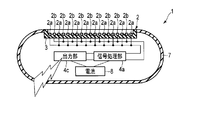
- the block diagram which shows the structure of the biosensor shown in FIG.
- the figure which shows the usage example of the biosensor shown in FIG. 1 schematically.
- the perspective view which shows roughly the biosensor which concerns on 2nd Embodiment of this invention.
- the perspective view which shows roughly the biosensor which concerns on 3rd Embodiment of this invention.
- the top view which shows the 1st process in manufacture of the biosensor shown to FIG.5 and FIG.6.
- FIG. 7B is a sectional view taken along line VIIb-VIIb of the structure shown in FIG. 7A.
- FIG. 8B is a cross-sectional view taken along line VIIIb-VIIIb of the structure shown in FIG. 8A.
- FIG. 9B is a cross-sectional view taken along line IXb-IXb of the structure shown in FIG. 9A.
- FIG. 10B is a cross-sectional view taken along line Xb-Xb of the structure shown in FIG. 10A.
- FIG. 11B is a cross-sectional view taken along line XIb-XIb of the structure shown in FIG. 11A.
- FIG. 12B is a cross-sectional view of the structure shown in FIG. 12A along the line XIIb-XIIb.
- FIG. 13B is a sectional view taken along line XIIIb-XIIIb of the structure shown in FIG. 13A.
- FIG. 15 is a sectional view taken along line XV-XV of the structure shown in FIG.
- the perspective view which shows schematically the electrode obtained by performing a 2nd process in manufacture of the biosensor which concerns on 4th Embodiment.
- Sectional drawing which shows the 3rd process in manufacture of the biosensor which concerns on 4th Embodiment.
- Sectional drawing which shows the 4th process in manufacture of the biosensor which concerns on 4th Embodiment.
- the figure which shows schematically the other modification of the biosensor shown in FIG. The figure which shows schematically the further another modification of the biosensor shown in FIG.
- FIG. 31 is a sectional view taken along line XXXIIa-XXXIIa in the structure shown in FIG. 30.
- FIG. 31 is a sectional view taken along line XXXIIb-XXXIIb in the structure shown in FIG. 30.
- FIG. 31 is a sectional view taken along line XXXIIc-XXXIIc in the structure shown in FIG. 30.
- FIG. 34 is a diagram schematically showing a second step of a method that can be used for manufacturing an electrode included in the biosensor shown in FIGS. 23 and 27, and is a cross-sectional view corresponding to FIG. 32B. It is a figure which shows schematically the 2nd process of the method which can be utilized for manufacture of the electrode which the biosensor shown in FIG.23 and FIG.27 contains, Comprising: Sectional drawing corresponding to FIG. 32C.
- FIG. 34 is a diagram schematically showing a second step of a method that can be used for manufacturing an electrode included in the biosensor shown in FIGS. 23 and 27, and is a cross-sectional view corresponding to FIG. 32B.
- FIG. 32 is a diagram schematically showing a third step of a method that can be used for manufacturing an electrode included in the biosensor shown in FIGS. 23 and 27, and is a cross-sectional view corresponding to FIG. 32A. It is a figure which shows schematically the 3rd process of the method which can be utilized for manufacture of the electrode which the biosensor shown in FIG.23 and FIG.27 contains, Comprising: Sectional drawing corresponding to FIG. 32B. It is a figure which shows schematically the 3rd process of the method which can be utilized for manufacture of the electrode which the biosensor shown in FIG.23 and FIG.27 contains, Comprising: Sectional drawing corresponding to FIG. 32C.
- FIG.23 and FIG.27 contains, Comprising: The top view which drew the structure obtained by a 3rd process from the back side.
- FIG.23 and FIG.27 contains, Comprising: The top view which drew the structure obtained by a 4th process from the back side.
- the side view which shows roughly the 1st example of the biosensor which concerns on 7th Embodiment of this invention.
- FIG. 43 is a sectional view taken along line XLIII-XLIII of the structure shown in FIG.
- the perspective view which shows roughly one process in manufacture of the biosensor which concerns on Example 3 which is a specific example of this invention.
- a biosensor has been invented that obtains a numerical value as a biomarker by electrochemically measuring and analyzing a component of a body fluid obtained from a living body.
- the biosensors described in Patent Documents 1 to 5 adopt an ex vivo method, and are adapted in form and method according to the target measurement system.
- the biosensor described in Patent Document 6 uses carbon as an electrode material for electrochemical measurement.
- the biosensors described in Patent Documents 7 and 8 include a control / processing device and components that transmit signals.
- the electrode which is the most important element when performing electrochemical measurements, is various in terms of the form, material, and manufacturing method, including cost. Whether it can be adapted to actual manufacturing.
- the measurement electrode can have various shapes according to the application.
- the measurement electrode is not a flat surface but a curved surface, thereby improving compatibility with various apparatuses.
- the electrode surface must be electrochemically stable.
- an electrode formed by partially coating a conductive material with an electrochemically inactive conductive material is supported by an insulating material so that the portion not coated with the conductive material is covered
- the electrochemically unstable conductive material comes into contact with the liquid.
- corrosion or the like of the conductive material occurs, and measurement cannot be performed with sufficient reliability.
- the coating made of a conductive material is thin and pinholes cannot be avoided at the manufacturing stage, sufficient reliability is still possible. Cannot be measured under
- noble metals such as gold and platinum are selected as the electrochemically stable conductive material. Since these substances are very expensive, they are formed as a thin film on a substrate and formed into an electrode shape by patterning. However, in order to avoid pinholes, it is necessary to ensure a certain film thickness, so that even a thin film has a high cost.
- Patent Document 6 it is possible to use carbon as an electrochemically stable and low-cost material.
- carbon is a material that is extremely difficult to process, and a thick and dense layer cannot be formed by vapor deposition or printing. For this reason, carbon has hardly been considered for use as an electrode of a biosensor.
- the general manufacturing method of the electrode which is a conductor can be distinguished into subtractive processing and additive processing.
- subtractive processing (1) physical processing such as cutting, polishing, molding, and laser processing is applied to an integral conductive material that is plate-shaped, linear, or massive, or chemical etching or the like is performed. (2) forming a layer made of a conductive material on an insulating substrate with a relatively large area and subjecting it to physical processing or chemical processing to form the shape of the electrode. And the method of doing.
- the electrodes obtained by the methods (1) to (4) can be partially covered with an insulating material such as resin. Further, another metal can be deposited on the electrode surface by a film forming method such as plating or vapor phase growth.
- the carbon electrode is obtained by the method (1), chemical processing can hardly be used.
- physical processing is performed on a material made of a carbon material such as glassy carbon, boron-doped diamond, and graphite. Therefore, with such a method, it is difficult to improve productivity by processing minute electrodes and batch processing.
- conductive carbon such as graphite, graphene and carbon nanotubes is deposited on the entire surface of the insulating substrate by vapor deposition, and a necessary portion of the obtained layer is masked. Cover and dry etch. However, it is difficult to increase the film thickness of the carbon layer formed by the vapor deposition method.
- the vapor phase growth method is used as in the method (2). Therefore, as described above, it is difficult to form the carbon layer with a large film thickness.
- a conductive layer / carbon layer is provided on a flat insulating substrate, so that it is used as an electrode.
- complicated processes such as dry etching using a resist and lift-off had to be performed in order to pattern the shape.
- a film having a uniform film thickness can be formed on a flat substrate.
- a film having a uniform film thickness can be formed for a substrate having a complicated shape such as a previously deformed substrate. It is difficult to form a carbon layer.
- a carbon layer forming method there are a carbon paste printing method, a glassy carbon or diamond polishing process, and a method in which various carbon materials are mixed with a polymer and applied in addition to the vapor phase growth method.
- a carbon paste printing method a glassy carbon or diamond polishing process
- various carbon materials are mixed with a polymer and applied in addition to the vapor phase growth method.
- Biosensors have restrictions on the shape of the electrode for various reasons, and thus there is a potential demand for enabling the formation of a carbon electrode having a complicated shape.
- the existing electrochemical sensors follow the progress of medical technology in the future, improve the reliability as a device, and in order to reduce the cost and improve the productivity so that it can be widely spread. There are many challenges.
- the biosensor according to the embodiment can solve one or more of the problems described above.
- the biological sensor according to the embodiment uses, for example, a numerical value serving as an index for grasping the characteristics and state of a living body, using a liquid collected from the living body or containing a minute living body as a liquid sample. Is a biosensor that is obtained ex vivo and electrically transmitted to the outside.
- the biological sensor described below uses an in-vivo liquid as a liquid sample, and acquires an in vivo (in vivo) numerical value serving as an index for grasping the characteristics and state of the living body. And a biosensor that electrically transmits it to the outside.
- the two or more electrodes are, for example, any of a pair of measurement electrodes, a pair of measurement electrodes and a reference electrode, and a combination of a pair of measurement electrodes and a reference electrode.
- the sample is, for example, a liquid sample.
- a liquid sample for example, blood, urine, sweat, tears, saliva, sebum, lymph fluid, gastric fluid, feces, semen, or nasal fluid, or a solution obtained by diluting it with a liquid such as water is used.
- a voltage is applied or a current is passed between the paired measurement electrodes, and a current or potential corresponding to the voltage or current is measured.
- the current is measured, if this measurement is continuously performed, the amount of electricity can be obtained by integrating the current with time.
- the potential difference between the measurement electrode and the reference electrode is measured.
- the potential difference between the reference electrode and one measurement electrode is kept constant, and the current flowing between the measurement electrodes is measured.
- a constant current is passed between the measurement electrodes, and the potential difference between the reference electrode and one measurement electrode is measured.
- the biosensor according to the embodiment employs a structure in which one or more electrodes include a base having a metal surface and a protective layer covering at least a part of the surface.
- This protective layer is a continuous film made of carbon and having a thickness of 1 ⁇ m or more.
- Carbon is electrochemically inert. Therefore, even if this protective layer is brought into contact with a living body or a liquid, it is difficult to cause deterioration. Moreover, since carbon is electrochemically inactive, it is stable to living organisms. Therefore, this protective layer has a small influence on the living body when it is brought into contact with the living body.
- this protective layer is a continuous film as described above. That is, this protective layer is not a porous film or a film composed of carbon particles, but a dense film, unlike those formed using carbon paste. And since this protective layer has sufficient thickness, possibility that a pinhole will exist is low. Therefore, this electrode has a very low possibility that the liquid penetrates the protective layer and comes into contact with the substrate.
- this protective layer is not a porous film or a film composed of carbon particles, but a continuous film. Therefore, this protective layer has high conductivity. Therefore, this biosensor is excellent in reliability and can be measured with high accuracy.
- this biosensor can be manufactured at a relatively low cost.
- the protective layer covers at least the entire region that can be contacted by the measurement target on the surface.
- the protective layer is made of carbon, it is difficult to join the lead wire to the protective layer using solder or the like.
- solder or the like When joining the lead wire to this electrode, for example, the metal surface of the base is partially exposed, and the lead wire is joined to the base at that position.
- a protective layer is formed on the entire metal surface of the substrate.
- a part of the protective layer is removed.
- one end of the lead wire is joined to the exposed portion of the metal surface of the base.
- a protective layer is formed on the entire surface of the base made of metal, and then the edge of the base is cut together with the protective layer thereon. Thereby, the metal is exposed at the position of the cut surface.
- a part of a plate having a surface made of metal is removed to obtain a structure including a base and a support portion connected thereto.
- a protective layer is formed on the metal surface of the structure. Thereafter, the substrate is separated from the support portion. Then, one end of the lead wire is joined to the exposed portion of the metal surface of the base.
- a mask is formed on a part of the metal surface of the substrate.
- a protective layer is formed on the entire exposed portion of the metal surface.
- the mask is removed from the metal surface.
- one end of the lead wire is joined to the exposed portion of the metal surface of the base.
- the protective layer covers the entire surface except for the joint portion between the metal surface of the substrate and the lead wire.
- the substrate can have various shapes.
- the two or more electrodes may be arranged parallel to each other or may be arranged so as to be inclined with respect to each other.
- the base body may have, for example, a coil shape or a leaf spring shape.
- this electrode may serve as the spring.
- the following method may be used for electrical connection between the electrode and the lead wire.
- a hole is provided in a substrate having a metal surface.
- a protective layer is formed on the entire exposed portion of the metal surface. Then, by inserting a pin or screw into the hole, the lead wire connected to the pin or screw can be electrically connected to the electrode.
- a through hole is provided in the base and a protective layer is formed on the entire exposed portion of the metal surface to form an electrode, for example, a pin, a screw or the like is inserted into the through hole, and the base is prepared separately, for example, metal. It is also possible to fix the electrode to a substrate having a surface and to electrically connect the substrate and the electrode. This makes it possible to separate the electrode and the sensor body from each other or to couple them as necessary. Therefore, for example, only the electrodes can be made disposable. Note that the protective layer described above may also be formed on the surface of a separately prepared substrate.
- this method forms a protective layer made of carbon by plating, the protective layer can be formed evenly on the side wall of the hole. That is, this method has an advantage that the metal surface is not exposed.
- the biological sensor may further include a processing unit (or an information processing unit) that is electrically connected to two or more electrodes and generates information about a measurement target from a current flowing between the electrodes or a voltage between the electrodes. Good.
- the biosensor may further include an output unit that outputs information to the outside of the biosensor.
- the biological sensor may further include a power supply unit and a control unit.
- the protective layer described above is formed by, for example, a plating method.
- a carbon plating technique that is implemented by I'M Sep Co., Ltd. using molten salt electrolysis.
- This technology uses an anodic oxidation reaction of carbide ions (C 2 2 ⁇ ) added to a molten salt such as chloride (see the following reaction formula), so that the surface of the material to be treated is an anode.
- a dense carbon layer is formed.
- the protective layer thus obtained typically includes a graphite structure, and is composed of a mixture of carbon atoms forming sp2 bonds and carbon atoms forming sp3 bonds. The details of this method are described in JP2009-120860.
- conductive carbon particles are contained in an electrolytic solution containing a metal to be deposited so that the substrate becomes a cathode.
- a method of forming a protective layer by causing an electrochemical reaction is a method of forming a protective layer by causing an electrochemical reaction.
- carbon particles for example, those containing a graphite structure and composed of a mixture of sp2 structure and sp3 structure are used.
- a metal to be deposited for example, in addition to noble metals such as gold, platinum, silver, rhodium and ruthenium, iron, nickel, cobalt, copper, chromium, zinc or alloys thereof can be used in an electrolytic plating solution made of an aqueous solution. A thing can be selected suitably.
- a non-aqueous dimethyl sulfone bath aluminum can be used as the metal to be deposited.
- the liquid sample to be subjected to biological sensing is acidic or alkaline or contains a compound capable of complexing the metal to be deposited at a relatively high concentration, it is preferable to use a noble metal.
- a noble metal When the liquid sample is neutral and does not contain a compound capable of complexing the metal to be deposited, various selections are possible. Whether it can be used as a metal to be deposited may be confirmed in advance by experiments.
- the protective layer obtained by such a method is not a pure carbon layer because the metal to be deposited surrounds the carbon particles and precipitates. However, it can be used by selecting the metal to be deposited in accordance with the target of biological sensing.
- the protective layer is formed by, for example, a plating method.
- a thick protective layer can be formed.
- a protective layer having a thickness of 1 to 5 ⁇ m can be formed.
- a protective layer having a uniform thickness can be formed even when the substrate has a complicated shape.
- the protective layer can be formed so as to cover at least a region of the metal surface of the substrate corresponding to a portion where the substrate is curved or bent.
- the protective layer includes the entire first main surface and the second main surface. And at least a part of the end face.
- the protective layer can be formed at a relatively low cost and with high productivity.
- this protective layer typically includes a graphite structure, and includes carbon atoms forming sp2 bonds and carbon atoms forming sp3 bonds. It consists of a mixture of
- the surface of the protective layer may be modified.
- glucose oxidase or an osmium compound may be immobilized on the surface of the protective layer.
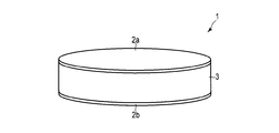
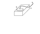
- FIG. 1 is a perspective view schematically showing a biosensor according to a first embodiment of the present invention.
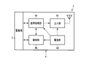
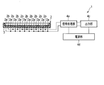
- FIG. 2 is a block diagram showing the configuration of the biosensor shown in FIG.
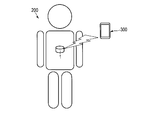
- FIG. 3 is a diagram schematically showing an example of use of the biosensor shown in FIG.
- the biological sensor 1 shown in FIGS. 1 and 2 is used by a living body 200, in this case a human, to obtain information about the living body 200 from the liquid in the living body 200.
- the biological sensor 1 transmits this information to the external device 300 wirelessly.
- the information regarding the living body 200 can be acquired in real time, for example.
- Information on the living body 200 may be stored in the living body sensor 1 and transmitted from the living body sensor 1 to the external device 300 wirelessly or by wire after the living body sensor 1 is discharged from the living body 200.
- the biosensor 1 has a flat, generally cylindrical shape like a general tablet, and the shape of the biosensor 1 is not limited to this.
- the biosensor 1 may have a flat elliptic cylinder or a long cylindrical shape, and may have a spherical shape or a spheroid shape.
- the biosensor 1 includes an electrode unit 2 and an electronic component 4 shown in FIG. 2, a support 3 shown in FIG. 1, and a battery (not shown).
- the electrode part 2 shown in FIG. 2 includes the electrodes 2a and 2b shown in FIG.
- One or both of the electrodes 2a and 2b include a base and a protective layer.
- both the electrodes 2a and 2b include a substrate and a protective layer described below.
- the substrate has a surface made of metal.
- the base is made of, for example, a metal or a composite of a metal and an insulator such as a resin.
- As the metal stainless steel or iron can be used.
- the base body has first and second main surfaces parallel to each other and end surfaces extending along the edges thereof.
- the substrate has a disk shape.
- the protective layer covers at least a part of the surface of the base made of metal.
- the protective layer is a continuous film made of carbon as described above.
- the protective layer covers the entire first main surface, a part of the second main surface, and the entire end surface of the substrate.
- the support 3 supports the electrodes 2a and 2b so as to be separated from each other.
- the support 3 is made of an insulator at least in contact with the electrodes 2a and 2b.
- As the insulator for example, medical plastic or ceramic can be used.
- the support 3 has a flat cylindrical shape.
- the support 3 supports the electrodes 2a and 2b such that one bottom surface faces the second main surface of the electrode 2a and the other bottom surface faces the second main surface of the electrode 2b.
- the support 3 has a hollow structure.
- the support 3 incorporates the electronic component 4 shown in FIG. 2 and a battery (not shown).
- the electronic component 4 shown in FIG. 2 includes a signal processing unit (or processing unit) 4a, a control unit 4b, an output unit 4c, and a power supply unit 4d.
- the signal processing unit 4 a and the control unit 4 b are electrically connected to the electrode unit 2.
- the controller 4b applies a voltage between the electrodes 2a and 2b, or allows a current to flow between them.
- the signal processing part 4a produces
- the voltage applied between the electrodes 2a and 2b by the control unit 4b or the magnitude of the current flowing between them may be, for example, constant or may be changed in a pulse waveform, and linearly according to the passage of time. It may be increased or decreased periodically, and may be changed over time according to a certain function.
- the signal processing unit 4a converts, for example, the magnitude of the current flowing between the electrodes 2a and 2b and the potential difference between them into a signal that can be easily transmitted to the output unit 4c.
- the signal processing unit 4a may further perform averaging, calculation according to a certain model, or the like.
- the power supply unit 4d is electrically connected to the signal processing unit 4a, the control unit 4b, and the output unit 4c.
- the power supply unit 4d appropriately distributes the power supplied from the battery to other elements of the electronic component 4. Alternatively, it may itself include a battery.
- the output unit 4c is electrically connected to the signal processing unit 4a.
- the output unit 4c transmits the information generated by the signal processing unit 4a to the external device 300 using wireless communication.
- wireless communication can be used, the risk of failure due to contamination of foreign matter inside the biosensor 1 is reduced, and hygiene benefits are also obtained.
- the signal processing unit 4a, the control unit 4b, the output unit 4c, and the power supply unit 4d are formed on one or more semiconductor chips. All of these may be formed on a single semiconductor chip, or they may be formed on separate semiconductor chips.
- a battery (not shown) is electrically connected to the power supply unit 4d.
- the battery supplies power to the power supply unit 4d.
- the biosensor 1 does not include a battery when, for example, power can be supplied wirelessly from the outside, or when a configuration in which a galvanic current generated by contact of metal with body fluid can be used is used. Also good.
- this biosensor 1 is used after drinking.
- the living body 200 analyzes the body fluid by drinking the biological sensor 1. Examples of places where body fluids are analyzed include, but are not limited to, the mouth, stomach, and intestines.
- the biosensor 1 performs an analysis at a predetermined periodic timing or always performs an analysis.
- the analysis result is temporarily stored in the biosensor 1 and transmitted to the external device 300 using wireless communication. Thereby, it becomes possible for a patient and a doctor to grasp a measurement result.
- FIG. 4 is a perspective view schematically showing a biosensor according to the second embodiment of the present invention.
- the biosensor 1 is for obtaining information related to a living body by contacting the living body.
- the biosensor 1 is brought into contact with, for example, the skin or the tongue during use.
- the biosensor 1 may be pressed against the skin or affixed to the skin.
- the biosensor 1 is used by being implanted in the body.
- the biosensor 1 can be used for measurement or acquisition of, for example, an electroencephalogram, an electrocardiogram, an electromyogram, or pH of gastric juice or blood.
- the biosensor 1 is substantially the same as the biosensor 1 described with reference to FIGS. 1 and 2 except that the following configuration is adopted. That is, in this biosensor 1, the support 3 supports both the electrodes 2a and 2b on one surface. The electrodes 2 a and 2 b protrude from the support surface of the support 3. When this structure is adopted, the electrodes 2a and 2b are easily brought into contact with the support.
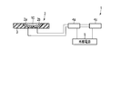
- FIG. 5 is a perspective view schematically showing a biosensor according to a third embodiment of the present invention. 6 is a cross-sectional view of a part of the biosensor of FIG.
- the biosensor 1 is a device that uses a liquid collected from a living body as a sample 10, that is, a device that is used ex vivo.
- the electrode unit 2 includes a pair of electrodes 2 a and 2 b and a support 3.
- the support 3 has a plate shape in which a concave portion for accommodating the sample 10 is provided on the upper surface.
- the electrodes 2a and 2b are installed in the recess.
- the signal processing unit 4a is electrically connected to the electrodes 2a and 2b and the external power source 5
- the output unit 4c is electrically connected to the signal processing unit 4a and the external power source 5.
- the signal processing unit 4a serves as the control unit 4b in addition to serving as the signal processing unit 4a described with reference to FIG.
- the output unit 4c serves as the output unit 4c described with reference to FIG.
- the external power supply 5 may be a DC power supply or an AC power supply.
- the biosensor 1 is manufactured, for example, by sequentially performing the following first to eighth steps.
- the electrodes 2a and 2b can be manufactured by the same method, the description regarding the manufacturing method of the electrode 2b is omitted here.
- FIGS. 5 and 6 are diagrams showing a first step in manufacturing the biosensor shown in FIGS. 5 and 6.
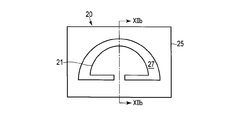
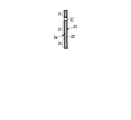
- 7A is a plan view
- FIG. 7B is a cross-sectional view taken along line VIIb-VIIb in FIG. 7A.
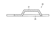
- a metal plate 20 shown in FIGS. 7A and 7B is prepared.
- the metal plate 20 includes a base body 21 and a support portion 25 of the electrode 2a.
- the metal plate 20 is provided with a slit 27.
- the base body 21 and the support part 25 are separated from each other via the slit 27 except for the connection part that connects them to each other.
- the material of the metal plate 20 it is easy to form, strength after forming, thermal expansion characteristics, melting point, ease of forming an oxide film, price, and a protective layer made of carbon on the surface of the metal plate Taking into account the formation of the method. Since a protective layer made of carbon is formed on the substrate 21, the electrochemical stability of the substrate 21 itself is not important.
- a material of the metal plate 20 for example, nickel, copper, iron, an alloy thereof, or stainless steel can be used.
- the substrate 21 is plate-shaped here, but may have other shapes such as a rod shape. Further, the base plate 21 may be deformed by subjecting the metal plate 20 to press working such as bending or drawing.
- the slit 27 can be formed by, for example, shearing, chemical etching, blasting, laser processing, or a combination thereof. For example, a plurality of processes may be combined in consideration of productivity and accuracy, such as bending a chemically etched material with a press and further cutting a part with a laser.
- FIGS. 5 and 6 are diagrams illustrating a second step in manufacturing the biosensor illustrated in FIGS. 5 and 6.
- 8A is a plan view
- FIG. 8B is a cross-sectional view taken along line VIIIb-VIIIb in FIG. 8A.
- a protective layer 22 made of carbon is formed on the entire surface of the metal plate 20 as shown in FIGS. 8A and 8B.
- the protective layer 22 is formed by, for example, a plating method. Thereby, the electrode 2a is obtained.
- FIGS. 5 and 6 are diagrams showing a third step in manufacturing the biosensor shown in FIGS. 5 and 6.
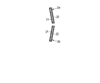
- 9A is a plan view
- FIG. 9B is a cross-sectional view taken along the line IXb-IXb in FIG. 9A.
- the base 21 is separated from the support portion 25 together with the protective layer 22 thereon.
- the joint portion between the base 21 and the support portion 25 is cut using a laser, a microcutter, or the like.
- the electrode 2a is obtained.
- the electrode 2b is obtained by the method similar to this. In these electrodes 2 a and 2 b, a region located on the cut surface of the surface of the base 21 is exposed, but the other region is covered with the protective layer 22.
- FIGS. 5 and 6 are diagrams showing a fourth step in manufacturing the biosensor shown in FIGS. 5 and 6.
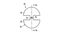
- 10A is a plan view
- FIG. 10B is a cross-sectional view taken along line Xb-Xb in FIG. 10A.
- the electrodes 2a and 2b are temporarily fixed as shown in FIGS. 10A and 10B.
- the electrodes 2a and 2b are arranged so that their main surfaces are inclined with respect to each other and their cut surfaces are diagonally opposed.
- FIGS. 5 and 6 are diagrams showing a fifth step in manufacturing the biosensor shown in FIGS. 5 and 6.
- 11A is a plan view
- FIG. 11B is a cross-sectional view taken along line XIb-XIb in FIG. 11A.
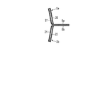
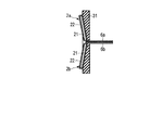
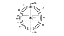
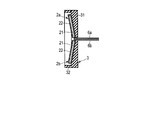
- one end of the lead line 6a is joined to the electrode 2a, and one end of the lead line 6b is joined to the electrode 2b.
- the lead wires 6a and 6b are preferably joined to the base 21 exposed at the cut surface. The lead wires 6a and 6b are separated so as not to be electrically short-circuited.
- FIGS. 5 and 6 are views showing a sixth step in manufacturing the biosensor shown in FIGS. 5 and 6.
- 12A is a plan view
- FIG. 12B is a cross-sectional view taken along line XIIb-XIIb in FIG. 12A.
- the electrodes 2a and 2b are supported by the support body 31 as shown in FIGS.
- the support body 31 supports each of the electrodes 2a and 2b so that one main surface is exposed and the other main surface is entirely covered.
- the support body 31 needs to be stable with respect to the liquid sample used for biological sensing.
- An organic resin is suitable as a material for the support body 31.
- the liquid sample should not enter between the support body 31 and the electrodes 2a and 2b so that the effective areas of the electrodes 2a and 2b are constant. Further, from the viewpoint of preventing the corrosion of the substrate 21, the liquid sample should not come into contact with the connection portion between the electrode 2a and the lead wire 6a or the connection portion between the electrode 2b and the lead wire 6b. Therefore, it is preferable to form the support body 31 so as to embed these connection portions or to form an insulating layer on the connection portions.
- FIGS. 5 and 6 are views showing a seventh step in manufacturing the biosensor shown in FIGS. 5 and 6.
- 13A is a plan view
- FIG. 13B is a cross-sectional view taken along line XIIIb-XIIIb in FIG. 13A.
- a wall 32 is provided on the upper surface of the support body 31 so as to surround the electrodes 2a and 2b. Thereby, the support body 3 including the support body 31 and the wall 32 is obtained.
- the wall 32 it is possible to make it difficult for the liquid sample to flow out. Further, when the wall 32 is provided, the liquid sample can be reliably brought into contact with the entire upper surfaces of the electrodes 2a and 2b.
- the material of the wall 32 is preferably the same as the material of the support body 31.
- the wall 32 can be formed in the step of forming the support body 31.
- the lead wires 6a and 6b are connected to an electronic component including the signal processing unit 4a and the output unit 4c shown in FIGS. 5 and 6, and the electrodes 2a and 2b are electrically connected to the signal processing unit 4a. Connecting.
- the electronic component includes one or more semiconductor chips and a printed wiring board on which the semiconductor chip is mounted
- the lead wires 6a and 6b are connected to terminals on the printed wiring board.
- the biosensor 1 shown in FIGS. 5 and 6 is obtained.
- the electrode part 2 may be detachable.
- the lead wires 6a and 6b are electrically connected to the electronic component via, for example, a connector. If the electrode part 2 is detachable, only the electrode part 2 can be exchanged.
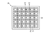
- FIG. 14 is a plan view showing a first step in manufacturing the biosensor according to the fourth embodiment of the present invention.
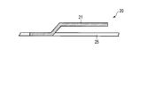
- FIG. 15 is a cross-sectional view taken along line XV-XV of the structure shown in FIG.
- FIG. 16 is a perspective view schematically showing an electrode obtained by performing the second step in the manufacture of the biosensor according to the fourth embodiment.
- FIG. 17 is a cross-sectional view showing a third step in the manufacture of the biosensor according to the fourth embodiment.
- FIG. 18 is a cross-sectional view showing a fourth step in the manufacture of the biosensor according to the fourth embodiment.
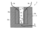
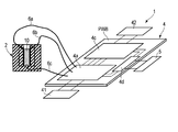
- FIG. 19 is a diagram schematically illustrating a biosensor according to the fourth embodiment, in which a part is a cross-sectional view and the other part is a perspective view.
- the biosensor 1 shown in FIG. 19 is a device that uses a liquid collected from a living body as the sample 10, that is, a device that is used ex vivo.
- the electrode portion 2 includes electrodes 2a, 2b and 2c, a support body 3, and lead wires 6a, 6b and 6c.
- the electrodes 2a and 2b are measurement electrodes.
- Each of the electrodes 2 a and 2 b includes a base 21 and a protective layer 22.
- the electrode 2c is a reference electrode.
- a silver / silver chloride electrode can be used as the reference electrode.
- Such a reference electrode is obtained by preparing a part having a surface made of metallic silver and chlorinating the surface to produce silver chloride.
- the support 3 has a recess.
- the support 3 supports the electrodes 2a and 2b on the side wall of the recess so that they face each other. Furthermore, the support 3 supports the electrode 2c at the bottom of the recess.
- One end of the lead wire 6a is joined to the base 21 of the electrode 2a.
- One end of the lead wire 6b is joined to the base 21 of the electrode 2b.
- One end of the lead wire 6c is joined to the electrode 2c.
- the other ends of the lead wires 6a, 6b, and 6c are electrically connected to the signal processing unit 4a shown in FIG.
- the electronic component 4 includes a signal processing unit 4a, a power supply unit 4d, and an output unit 4c.
- the signal processing unit 4a is electrically connected to an interface 41 for inputting data thereto.
- the signal processing unit 4a serves as the control unit 4b in addition to serving as the signal processing unit 4a described with reference to FIG.
- the power supply unit 4d is electrically connected to the external power supply 5, the signal processing unit 4a, and the output unit 4c.
- the output unit 4c is electrically connected to the signal processing unit 4a and an interface 42 for transferring data from here to the outside.
- This biological sensor 1 is manufactured by the following method, for example. First, the metal plate 20 shown in FIGS. 14 and 15 is prepared. The metal plate 20 is obtained by forming a base body 21 and a support portion 25 by providing a slit 27 in a flat plate made of metal, and further bending the base body 21 with respect to the support portion 25 by bending.
- the protective layer 22 is formed and the electrodes 2a and 2b are separated from the support portion 25 by the same method as described in the third embodiment.
- the electrodes 2a and 2b thus obtained have the base 21 exposed at their cut surfaces as shown in FIG.
- the electrodes 2a and 2b are supported by the insulating parts 33a and 33b, respectively.
- the insulating component 33a supports the electrode 2a so that one main surface is exposed and the other main surface is entirely covered by the insulating component 33a.
- the insulating component 33b supports the electrode 2b so that one main surface thereof is exposed and the other main surface is entirely covered by the insulating component 33b.
- one end of the lead line 6a and one end of the lead line 6b shown in FIG. 17 are joined to the electrode 2a and the electrode 2b, respectively, by the same method as described in the third embodiment.
- the lead wires 6 a and 6 b are joined to the exposed portion of the base 21.
- the electrode 2a integrated with the insulating component 33a and the electrode 2b integrated with the insulating component 33b are placed in the cavity of the mold (not shown), and the exposed main surfaces thereof are those of the mold not shown. Arrange the cores so that they face each other. At this time, the electrode 2c shown in FIG. 18 is installed below the core.
- a resin is injected into the mold.
- a support body 33c shown in FIG. 18 is obtained.
- the electrode part 2 shown in FIG. 18 is obtained by disassembling the mold.
- the biosensor 1 is obtained by electrically connecting the electrode unit 2 to the electronic component 4.
- the lead wire 6a or 6b is joined to the exposed portion of the metal surface of the base 21.
- the electrical connection between the electrode 2a and the lead wire 6a and the electrical connection between the electrode 2b and the lead wire 6b may be performed by other methods.
- FIG. 20 is a perspective view schematically showing a first step in the connection method according to the modification.
- FIG. 21 is a perspective view schematically showing a second step in the connection method according to the modification.
- this method first, holes are provided in a substrate having a metal surface. Next, a protective layer is formed on the entire exposed portion of the metal surface. Thereby, the electrode 2a shown in FIG. 20 is obtained.
- the protective layer 22 is preferably formed so as to cover not only the outer surface of the base but also the side wall of the through hole.
- the pin 28 shown in FIG. 20 is inserted into the previous hole as shown in FIG. Note that other parts such as screws may be used instead of the pins 28.
- the lead wire 6 a is joined to the pin 28.
- the lead wire 6a may be joined to the pin 28 before being inserted into the hole.
- the protective layer described above may also be formed on the surface of the pin 28.
- the electrode 2a and the lead wire 6a are electrically connected. Further, the electrode 2b and the lead wire 6b are electrically connected by the same method.
- the electrodes 2a and 2b can be electrically connected to other conductive members by the following method.
- FIG. 22 is a perspective view schematically showing a connection method according to another modification.
- a through-hole is provided in a substrate having a metal surface.
- a protective layer is formed on the entire exposed portion of the metal surface.
- the electrode 2a provided with the through hole is obtained.
- the protective layer is preferably formed so as to cover not only the outer surface of the base but also the side wall of the through hole.
- this electrode 2a and a separately prepared substrate 29 are overlaid.
- the base 29 is provided with a hole communicating with the through hole of the electrode 2a.
- a conductive base having a surface made of metal is used as the base 29, for example.
- Such a substrate 29 may be entirely made of metal, or may be an insulator coated with a metal layer. Note that the protective layer described above may also be formed on the surface of the substrate 29.
- the pin 28 is inserted into the through hole of the electrode 2 a and the hole of the base 29 in a state where the electrode 2 a and the base 29 are overlapped. Thereby, the electrode 2a and the base body 29 are integrated and electrically connected.
- the electrode 2b can also be manufactured and integrated with the substrate 29 by the same method as described for the electrode 2a.
- the electrodes 2a and 2b can be attached to and detached from the sensor body. Therefore, for example, at least one of the electrodes 2a and 2b can be made disposable. Further, according to the plating, a protective layer can be uniformly formed on the side wall of the hole. That is, this method has an advantage that the metal surface is not exposed.
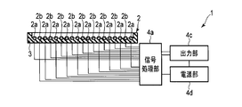
- FIG. 23 is a diagram schematically showing a biosensor according to a fifth embodiment of the present invention. Similar to the biosensors according to the third and fourth embodiments, the biosensor 1 is an apparatus that uses a liquid collected from a living body as a sample 10, that is, an apparatus that uses ex vivo. This biosensor 1 is different from the biosensors according to the third and fourth embodiments in that it includes a plurality of sets of electrodes 2a and electrodes 2b.
- the electrodes 2a are electrically connected to each other and the electrodes 2b are electrically connected to each other.
- the electrodes 2a are electrically insulated from each other, and the electrodes 2b are electrically insulated from each other. May be. In the latter case, different biomarkers can be detected from the same liquid sample by applying different surface modifications to one electrode pair and another electrode pair. The surface modification may be performed on both the electrodes 2a and 2b, or may be performed on only one of them.
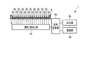
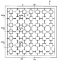
- FIG. 24 is a diagram schematically showing a modification of the biosensor shown in FIG.
- the electrodes 2a are electrically connected to each other, and the electrodes 2b are electrically connected to each other.
- the electrodes 2a are electrically insulated from each other and are separately electrically connected to the signal processing unit 4a, and the electrodes 2b are electrically insulated from each other.
- the signal processing unit 4a is electrically connected separately.
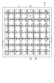
- FIG. 25 is a diagram schematically showing another modification of the biosensor shown in FIG.
- the biosensor 1 shown in FIG. 25 is the same as the biosensor 1 shown in FIG. 23 except that the biosensor 1 further includes a selection / reading unit 4e.
- the selection / reading unit 4e is electrically connected to the electrodes 2a and 2b and the signal processing unit 4a. For example, the selection / reading unit 4e selects a set of one of the electrodes 2a and one of the electrodes 2b, and supplies a signal obtained from the electrodes 2a and 2b to the signal processing unit 4a. The selection / reading unit 4e may sequentially select a set of one of the electrodes 2a and one of the electrodes 2b and continuously supply signals obtained from the electrodes 2a and 2b to the signal processing unit 4a.
- FIG. 26 shows still another modification of the biosensor shown in FIG.
- the biosensor 1 shown in FIG. 26 is the same as the biosensor 1 shown in FIG. 23 except for the following points.
- the biological sensor 1 includes a plurality of scanning lines L1, a plurality of signal lines L2, a plurality of power supply lines L3, and a plurality of selection circuits (not shown).
- the plurality of scanning lines L1 extend in the X direction and are arranged in the Y direction intersecting the X direction.
- Each of the plurality of signal lines L2 extends in the Y direction and is arranged in the X direction. These signal lines L2 are electrically insulated from the scanning line L1 and arranged so as to intersect the scanning line L1.
- Electrodes 2a and 2b are connected to each pixel circuit.
- Each pixel circuit has a selection transistor in which a gate electrode is connected to the scanning line, one of the source and drain electrodes is connected to the signal line, and the other of the source and drain electrodes is connected to the pixel circuit, and is connected to the scanning line L1.
- each selection transistor connects each pixel circuit to the signal line, and outputs each pixel circuit to the writing / reading unit.
- the OFF signal is supplied to the scanning line L1
- the pixel circuit is insulated from the signal line L2, and each pixel circuit is separated from the writing / reading unit.
- the biosensor 1 further includes a scanning unit 4f and a writing / reading unit 4g.
- the scanning unit 4f is electrically connected to the signal processing unit 4a and the scanning line L1.
- the scanning unit 4f sequentially selects the scanning line L1 based on the control signal supplied from the signal processing unit 4a, supplies an ON signal to the selected scanning line L1, and supplies an OFF signal to the non-selected scanning line L1. Supply.
- the writing / reading unit 4g is connected to the signal processing unit 4a and the signal line L2. For example, the writing / reading unit 4g performs the writing operation as an electrode bias condition for the pixel circuit selected by the scanning line. A voltage setting and a current setting are written, and a current signal and a voltage signal are read from the pixel circuit selected by the scanning line as a reading operation according to the bias condition.
- the biosensor 1 reads out signals by, for example, line-sequential driving.
- the number of signals equal to the product of the number M of the scanning lines L1 and the number N of the signal lines L2 can be obtained. That is, signals from M ⁇ N measurement points distributed two-dimensionally can be obtained. Therefore, for example, a two-dimensional distribution of signal intensity can be obtained. Further, it is possible to examine the change with time of this two-dimensional distribution by repeatedly reading out the signal.
- this biosensor 1 is used for the purpose of detecting a component involved in metabolism in a cell, that is, a substrate that is a starting material of metabolism or a metabolite that is a final product or intermediate product of metabolism, It is also possible to estimate the total amount of the previous component from the signal obtained from the electrode pair each consisting of one and one of the electrodes 2b.
- this biosensor 1 can detect different biomarkers from the same liquid sample by applying different surface modifications to a certain electrode pair and another electrode pair.
- some electrode pairs can be used for measurement, and some other electrode pairs can be used for calibration.
- a signal obtained from an electrode pair that has been subjected to surface modification can be calibrated with a signal obtained from an electrode pair that has not undergone surface modification, for example, by subjecting only some electrode pairs to surface modification.
- the influence of environmental variations such as temperature and manufacturing variations on the measurement result can be reduced.
- the electrodes 2a and 2b will change its characteristics when energized.
- at least one of the electrodes 2a and 2b may be deteriorated by energization or irreversibly adsorb a substance contained in the liquid sample.
- a part of electrode pairs are used for measurement, and then another part of electrode pairs are used for measurement.
- the lifetime of the sensor 1 can be extended.
- the electrode pairs are arranged so that the measurement points are distributed in a plane, but the electrode pairs may be arranged so that the measurement points are distributed in the space. In this case, a two-dimensional distribution of signal intensity can be obtained.
- FIG. 27 is a diagram schematically showing a biosensor according to a sixth embodiment of the present invention. This biosensor 1 is used by drinking, like the biosensor according to the first embodiment.
- the biosensor 1 includes a housing 7.
- the housing 7 supports the electrode portion 2 so that the electrodes 2a and 2b are exposed.
- the housing 7 includes a signal processing unit 4a, an output unit 4c, and a battery (battery) 8.
- This biosensor 1 includes a plurality of pairs of electrodes 2a and 2b, similarly to the biosensor according to the fifth embodiment.
- the electrodes 2a are electrically connected to each other and the electrodes 2b are electrically connected to each other.
- the electrodes 2a are electrically insulated from each other, and the electrodes 2b are electrically insulated from each other. May be.
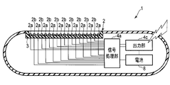
- FIG. 28 is a diagram schematically showing a modification of the biosensor shown in FIG.
- the biosensor 1 shown in FIG. 27 includes a plurality of sets of electrodes 2a and electrodes 2b, similarly to the biosensor according to the fifth embodiment.
- the electrodes 2a are electrically connected to each other, and the electrodes 2b are electrically connected to each other.
- the electrodes 2a are electrically insulated from each other and electrically connected to the signal processing unit 4a separately, and the electrodes 2b are electrically insulated from each other.
- the signal processing unit 4a is electrically connected separately.
- this configuration for example, separate signals can be obtained from a plurality of sets each composed of one of the electrodes 2a and one of the electrodes 2b.
- FIG. 29 is a diagram schematically showing another modification of the biosensor shown in FIG.
- the biosensor 1 shown in FIG. 29 is the same as the biosensor 1 shown in FIG. 27 except that it further includes a selection / reading unit 4e.
- the selection / reading unit 4e is electrically connected to the electrodes 2a and 2b and the signal processing unit 4a. For example, the selection / reading unit 4e selects a set of one of the electrodes 2a and one of the electrodes 2b, and supplies a signal obtained from the electrodes 2a and 2b to the signal processing unit 4a. The selection / reading unit 4e may sequentially select a set of one of the electrodes 2a and one of the electrodes 2b and continuously supply signals obtained from the electrodes 2a and 2b to the signal processing unit 4a.
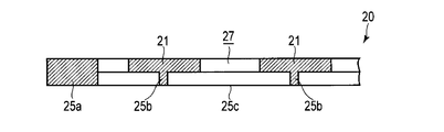
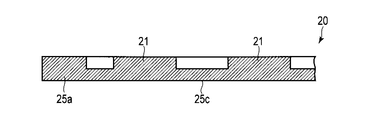
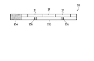
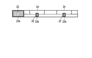
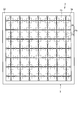
- FIG. 30 is a plan view schematically showing a first step of a method that can be used for manufacturing an electrode included in the biosensor shown in FIGS. 23 and 27.
- FIG. 31 is a plan view depicting the structure shown in FIG. 30 from the back side.
- 32A is a cross-sectional view of the structure shown in FIG. 30 taken along line XXXIIa-XXXIIa.
- 32B is a cross-sectional view taken along line XXXIIb-XXXIIb of the structure shown in FIG.
- 32C is a cross-sectional view taken along line XXIIc-XXXIIc of the structure shown in FIG.
- the metal plate 20 shown in FIGS. 30, 31, and 32A to 32C is prepared.
- the metal plate 20 includes base bodies 21 arranged vertically and horizontally and a support portion that supports them.
- the metal plate 20 has a slit 27.
- the support part includes a frame-like part 25a and linear parts 25b and 25c.
- the linear portions 25b extend in the vertical direction and are arranged in the horizontal direction.
- Each of the linear portions 25c extends in the horizontal direction and is arranged in the vertical direction.
- the linear portions 25b and 25c form a lattice.
- the thicknesses of the linear portions 25b and 25c are equal to each other and smaller than the thickness of the frame-like portion 25a.
- the base 21 is located on the lattice point of the lattice formed by the linear portions 25b and 25c.
- the sum of the thickness of the base 21 and the thickness of the linear portion 25b or 25c is equal to the thickness of the frame-like portion 25a.
- the metal plate 20 is manufactured by, for example, the following method. First, a first recess is formed on one surface of a flat plate made of metal. The first recess is formed at the position of the linear portions 25 b and 25 c and the slit 27.
- a second recess is formed on the other surface of the previous flat plate.
- the second recess is formed at a position that does not correspond to any of the frame-like portion 25a and the linear portions 25b and 25c.
- the second recess is formed so as to be connected to the first recess at the position of the slit 27.
- the metal plate 20 is obtained as described above.
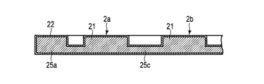
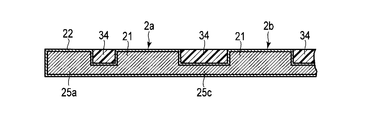
- (Second step) 33A to 33C are diagrams schematically illustrating a second step of a method that can be used for manufacturing an electrode included in the biosensor illustrated in FIGS. 23 and 27.
- 33A, 33B, and 33C are cross-sectional views corresponding to FIGS. 32A, 32B, and 32C, respectively.
- the protective layer 22 is formed on the entire surface of the metal plate 20 as shown in FIGS. 33A to 33C.
- the protective layer 22 is formed by the same method as described in the third embodiment.
- the electrodes 2a and 2b are obtained.
- the electrodes 2a and 2b are arranged in a checkered pattern.
- the electrodes 2a and 2b may be arranged in other ways.
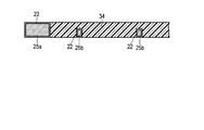
- or 33C is a figure which shows schematically the 3rd process of the method which can be utilized for manufacture of the electrode which the biosensor shown in FIG.23 and FIG.27 contains.
- 34A, 34B, and 34C are cross-sectional views corresponding to FIGS. 32A, 32B, and 32C, respectively.
- FIG. 35 is a diagram schematically showing a third step of a method that can be used for manufacturing an electrode included in the biosensor shown in FIGS. 23 and 27, and a structure obtained by the third step is drawn from the back side.
- FIG. 35 is a diagram schematically showing a third step of a method that can be used for manufacturing an electrode included in the biosensor shown in FIGS. 23 and 27, and a structure obtained by the third step is drawn from the back side.
- the first and second recesses are embedded with a support layer 34 made of resin.
- the support body 3 which consists of the support body layer 34 and the frame-shaped part 25a and supported the electrodes 2a and 2b is formed.
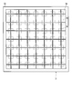
- FIG. 36 is a diagram schematically showing a fourth step of a method that can be used for manufacturing an electrode included in the biosensor shown in FIGS. 23 and 27, and a structure obtained by the fourth step is drawn from the back side.
- FIG. 36 is a diagram schematically showing a fourth step of a method that can be used for manufacturing an electrode included in the biosensor shown in FIGS. 23 and 27, and a structure obtained by the fourth step is drawn from the back side.
- the linear portion 25b is cut at the position Pb and the linear portion 25c is cut at the position Pc.
- the electrodes 2a and 2b are electrically insulated from each other.
- the electrode unit 2 shown in FIGS. 23 and 27 is obtained.
- the electrode portion 2 may be provided with the wall 32 described with reference to FIG. 13B.
- the electrode part 2 obtained in this way can be made flexible by making the support body layer 34 and the frame-shaped part 25a flexible.
- ⁇ Seventh embodiment> 37 to 39 are side views schematically showing examples of the biosensor according to the seventh embodiment of the present invention.
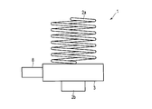
- the biosensor 1 shown in FIG. 37 includes electrodes 2a and 2b, a support 3, a battery 8, and a storage / output unit 9.
- the electrode 2a has a coil shape.
- the electrode 2a can function as a spring.
- the electrode 2b has a column shape.
- the electrode 2b is located in the expansion / contraction direction with respect to the electrode 2a.
- the support 3 is located between the electrodes 2a and 2b.
- the support 3 has a hollow structure and incorporates an electronic component including a signal processing unit.
- the battery 8 is detachably attached to the support 3.
- the battery 8 supplies power to the electronic components built in the support 3.
- the storage / output unit 9 is attached to the support 3.
- the storage / output unit 9 has a built-in storage device and stores information generated by the signal processing unit. Then, the storage / output unit 9 transmits this information to an external device wirelessly or by wire.
- the biosensor 1 does not include the storage / output unit 9 and the biosensor described with reference to FIG. 37 except that the electronic component built in the support 3 further includes an output unit and the like. It is the same.
- the biosensor 1 shown in FIG. 39 is the same as the biosensor described with reference to FIG. 37 except that the electrode 2b has the same structure as the electrode 2a. Also in the biosensor 1 shown in FIG. 38, the electrode 2b may have the same structure as the electrode 2a. Further, at least one of the electrodes 2a and 2b may have a leaf spring shape and can function as a spring.
- FIG. 40 is a diagram schematically showing one usage example of the biosensor according to the seventh embodiment of the present invention.
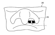
- FIG. 41 is a diagram schematically showing another usage example of the biosensor according to the seventh embodiment of the present invention.
- the biosensor 1 can be installed in the ear 201 as shown in FIG.
- sweat can be used as a liquid sample.
- the biosensor 1 can be installed in the nose 202 as shown in FIG.
- a runny nose can be used as the liquid sample.
- the biological sensor 1 may further incorporate a temperature sensor. For example, by installing the biological sensor 1 in the ear 201 or the nose 202 and constantly measuring the body temperature, it is possible to check the physiological cycle, the presence of pregnancy, or the like.
- the biosensor 1 may incorporate a heart rate monitor. For example, when the biosensor 1 is installed in the ear 201 or the nose 202 and the heart rate is constantly measured, an inspection for arrhythmia and the like can be performed.
- the biosensor 1 may further have a function of charging itself or its surroundings. For example, when the biosensor 1 is installed in the nose 202 and the nose 202 is positively charged, the entry of pollen into the nose 202 can be suppressed. Moreover, when the biosensor 1 is installed in the nose 202 and the biosensor 1 or the electrode 2a or 2b is negatively charged, pollen is collected, and the invasion of pollen into the back of the nose can be suppressed. it can. Further, when the living body sensor 1 is installed in the ear 201 or the nose 202 and the living body 200 is negatively charged, pollen can be adsorbed to the body and invasion of pollen into the nose 202 can be suppressed.
- the biosensor 1 may further have a function of generating electromagnetic waves. Pollen can be decomposed using electromagnetic waves.
- the biosensor 1 installed in the ear 201 may further have a function as a hearing aid or an earphone.
- Example 1 In this example, a biosensor was manufactured by the method described below, and measurement using this biosensor was performed.
- a stainless steel (SUS304) plate having a thickness of 0.3 mm was processed to obtain a metal plate 20 shown in FIGS. 14 and 15. Specifically, this processing was performed by the following method. First, a photosensitive etching resist was applied to both surfaces of a stainless steel plate. These resist layers were subjected to pattern exposure and developed to form resist patterns on both surfaces of the stainless steel plate. Next, stainless steel was etched using these resist patterns as an etching mask. As an etchant, a ferric chloride solution was used. Then, the metal plate 20 which has the slit 27 was obtained by peeling a resist pattern. Next, bending was performed so that the base 21 was lifted with respect to the support portion 25. Here, the size of the rectangular portion of the base 21 was 3.3 mm ⁇ 3.3 mm, and the base 21 was lifted by 0.5 mm with respect to the support portion 25.
- a continuous film made of carbon having a thickness of 3 ⁇ m was formed as the protective layer 22 shown in FIG. 16 on the entire surface of the metal plate 20 by plating.
- the protective layer 22 was formed by immersing the metal plate 20 in a molten salt containing calcium carbide (LiCl—KCl—CaCl 2 : 500 ° C.) and performing anodic polarization.
- insulating parts 33a and 33b shown in FIG. 17 were attached to a jig (not shown). Subsequently, the electrodes 2a and 2b were pressure-bonded to the insulating parts 33a and 33b, respectively.
- the distance between the electrodes 2a and 2b was about 2 mm.
- one end of the lead wire 6a and one end of the lead wire 6b shown in FIG. 17 were joined to the electrode 2a and the electrode 2b, respectively. Copper wires were used as the lead wires 6a and 6b.
- the lead wires 6a and 6b were joined to the exposed portion of the base 21 using a conductive paste.
- Example 2 In this example, a biosensor was manufactured by the method described below, and measurement using this biosensor was performed.
- a stainless steel (SUS304) plate having a thickness of 0.3 mm was processed to obtain a metal plate 20 shown in FIGS. 30, 31, and 32 ⁇ / b> A to 32 ⁇ / b> C. Specifically, this processing was performed by the following method. First, a photosensitive etching resist was applied to both surfaces of a stainless steel plate. These resist layers were subjected to pattern exposure and developed to form resist patterns on both surfaces of the stainless steel plate. Next, stainless steel was etched using these resist patterns as an etching mask. As an etchant, a ferric chloride solution was used. Then, the metal plate 20 which has the slit 27 was obtained by peeling a resist pattern.
- the dimension of the surface of the base body 21 having a quadrangular shape was set to 0.8 mm ⁇ 0.8 mm.
- a continuous film made of carbon having a thickness of 3 ⁇ m was formed as a protective layer 22 shown in FIGS. 33A to 33C on the entire surface of the metal plate 20 by plating.
- the protective layer 22 was formed by immersing the metal plate 20 in a molten salt containing calcium carbide (LiCl—KCl—CaCl 2 : 500 ° C.) and performing anodic polarization.
- the support layer 34 was cut into a lattice shape so that a cutting line extending in the horizontal direction passed through the position Pb and a cutting line extending in the vertical direction passed through the position Pc.
- the first composite including the electrode 2a and a part of the support layer 34, the second composite including the electrode 2b and the other part of the support layer 34, and a structure similar to them.
- a third composite having Next, the 1st thru
- (F) Preparation of electronic component The component shown in FIG. 19 was prepared. Specifically, a semiconductor chip including the signal processing unit 4a, a semiconductor chip including the output unit 4c, and a semiconductor chip including the power supply unit 4d were prepared. Moreover, the printed wiring board PWB which mounts these was also prepared.
- an interface 41 for inputting data was electrically connected to the signal processing unit 4a.
- an interface 42 for transferring data from here to the outside is electrically connected to the output unit 4c.
- the external power supply 5 was electrically connected to the power supply part 4d. As described above, the biosensor 1 shown in FIG. 19 was completed.
- H 2 O 2 and NO 2 ⁇ are added to phosphate buffered saline (pH 7.2), a first solution containing both H 2 O 2 and NO 2 ⁇ at a concentration of 1 mM, and H 2 A second solution containing O 2 at a concentration of 2 mM and NO 2 ⁇ at a concentration of 1 mM and a third solution containing both H 2 O 2 and NO 2 ⁇ at a concentration of 2 mM were prepared.
- each of these solutions was used as the sample 10 shown in FIG. Specifically, the amount of each sample 10 was 1 mL. A voltage of 0.4 V was applied between the reference electrode and the electrode 2a, and a voltage of 0.9 V was applied between the reference electrode and the electrode 2b. The electrode 2c was used as a common counter electrode. Then, the current flowing through the electrodes 2a and 2b was measured 60 seconds after the start of voltage application. Some of the measurement conditions are shown in Table 1 below. The results of this measurement are shown in Table 2 below.
- FIG. 42 is a plan view schematically showing one step in manufacturing a biosensor according to Example 3 of the present invention.
- 43 is a cross-sectional view of the structure shown in FIG. 42 taken along line XLIII-XLIII.
- FIG. 44 is a perspective view schematically showing one step in manufacturing a biosensor according to Example 3 of the present invention.
- a biosensor was manufactured by the method described below, and measurement using this biosensor was performed.
- Stainless steel (SUS304) having a thickness of 0.3 mm was processed to obtain a metal plate 20 shown in FIGS. Specifically, this processing was performed by the following method. First, a photosensitive etching resist was applied to both surfaces of a stainless steel plate. These resist layers were subjected to pattern exposure and developed to form resist patterns on both surfaces of the stainless steel plate. Next, stainless steel was etched using these resist patterns as an etching mask. As an etchant, a ferric chloride solution was used. Then, the metal plate 20 which has the slit 27 was obtained by peeling a resist pattern. Next, bending was performed so that the base 21 partially lifted with respect to the metal plate 20. Here, the length of the base 21 was 8 mm, and the base 21 was lifted 2 mm with respect to the support portion 25.
- a continuous film made of carbon having a thickness of 3 ⁇ m was formed on the entire surface of the metal plate 20 as the protective layer 22 shown in FIGS. 33A to 33C by plating.
- the protective layer 22 was formed by immersing the metal plate 20 in a molten salt containing calcium carbide (LiCl—KCl—CaCl 2 : 500 ° C.) and performing anodic polarization.
- one end of the lead line 6a and one end of the lead line 6b shown in FIG. 19 were joined to the electrodes 2a and 2b, respectively. Copper wires were used as the lead wires 6a and 6b.
- the lead wires 6a and 6b were joined to the portion of the substrate 21 protruding from the back surface of the support 35 using a conductive paste.
Landscapes
- Health & Medical Sciences (AREA)
- Life Sciences & Earth Sciences (AREA)
- Physics & Mathematics (AREA)
- Molecular Biology (AREA)
- Pathology (AREA)
- General Health & Medical Sciences (AREA)
- Chemical & Material Sciences (AREA)
- Engineering & Computer Science (AREA)
- Biomedical Technology (AREA)
- Veterinary Medicine (AREA)
- Surgery (AREA)
- Animal Behavior & Ethology (AREA)
- Medical Informatics (AREA)
- Public Health (AREA)
- Heart & Thoracic Surgery (AREA)
- Biophysics (AREA)
- Chemical Kinetics & Catalysis (AREA)
- Analytical Chemistry (AREA)
- Immunology (AREA)
- General Physics & Mathematics (AREA)
- Biochemistry (AREA)
- Electrochemistry (AREA)
- Hematology (AREA)
- Optics & Photonics (AREA)
- General Chemical & Material Sciences (AREA)
- Medicinal Chemistry (AREA)
- Food Science & Technology (AREA)
- Urology & Nephrology (AREA)
- Measurement Of The Respiration, Hearing Ability, Form, And Blood Characteristics Of Living Organisms (AREA)
Abstract
Description
本発明者らが、本発明を発明するに際して、先行技術について見出した問題点を以下に記載する。
実施形態に係る生体センサは、上述した課題の1以上を解決し得るものである。
また、炭素は、電気化学的に不活性であるので、生体に対しても安定である。それ故、この保護層は、生体に接触させた場合に、生体に及ぼす影響が小さい。
従って、この生体センサは、信頼性に優れており、高い精度での測定が可能である。
C2 2- → 2C(めっき膜) + 2e-
このようにして得られる保護層は、典型的には、グラファイト構造を含み、sp2結合を形成している炭素原子とsp3結合を形成している炭素原子との混合体からなる。なお、この方法の詳細は、特開2009-120860に記載されている。
CO3 2- + 4e- → C + 3O2-
なお、この方法の詳細は、特開2006-169554に記載されている。
それ故、この技術によれば、今後の医療技術の進歩に追随し、装置としての信頼性を向上させ、低コスト化や生産性の向上を達成することが可能になる。
図1は、本発明の第1実施形態に係る生体センサを概略的に示す斜視図である。図2は、図1に示す生体センサの構成を示すブロック図である。図3は、図1に示す生体センサの使用例を概略的に示す図である。
図4は、本発明の第2実施形態に係る生体センサを概略的に示す斜視図である。
この生体センサ1は、生体に接触させて、生体に関する情報を得るためのものである。
図5は、本発明の第3実施形態に係る生体センサを概略的に示す斜視図である。図6は、図5の生体センサの一部について断面を描いた図である。
図7A及び7Bは、図5及び図6に示す生体センサの製造における第1工程を示す図である。図7Aは平面図であり、図7Bは図7AのVIIb-VIIb線に沿った断面図である。
図8A及び8Bは、図5及び図6に示す生体センサの製造における第2工程を示す図である。図8Aは平面図であり、図8Bは図8AのVIIIb-VIIIb線に沿った断面図である。
図9A及び9Bは、図5及び図6に示す生体センサの製造における第3工程を示す図である。図9Aは平面図であり、図9Bは図9AのIXb-IXb線に沿った断面図である。
図10A及び10Bは、図5及び図6に示す生体センサの製造における第4工程を示す図である。図10Aは平面図であり、図10Bは図10AのXb-Xb線に沿った断面図である。
図11A及び11Bは、図5及び図6に示す生体センサの製造における第5工程を示す図である。図11Aは平面図であり、図11Bは図11AのXIb-XIb線に沿った断面図である。
図12A及び12Bは、図5及び図6に示す生体センサの製造における第6工程を示す図である。図12Aは平面図であり、図12Bは図12AのXIIb-XIIb線に沿った断面図である。
図13A及び13Bは、図5及び図6に示す生体センサの製造における第7工程を示す図である。図13Aは平面図であり、図13Bは図13AのXIIIb-XIIIb線に沿った断面図である。
第8工程では、引き出し線6a及び6bを、図5及び図6に示す信号処理部4a及び出力部4cを含んだ電子部品に接続して、電極2a及び2bを信号処理部4aに電気的に接続する。例えば、この電子部品が、1以上の半導体チップとこれを搭載したプリント配線板とを含んでいる場合、引き出し線6a及び6bはプリント配線板上の端子に接続する。
以上のようにして、図5及び図6に示す生体センサ1を得る。
図14は、本発明の第4実施形態に係る生体センサの製造における第1工程を示す平面図である。図15は、図14に示す構造のXV-XV線に沿った断面図である。図16は、第4実施形態に係る生体センサの製造において第2工程を行うことによって得られる電極を概略的に示す斜視図である。図17は、第4実施形態に係る生体センサの製造における第3工程を示す断面図である。図18は、第4実施形態に係る生体センサの製造における第4工程を示す断面図である。図19は、第4実施形態に係る生体センサを概略的に示す図であって、一部を断面図とし、他の部分を斜視図とした図である。
先ず、図14及び図15に示す金属板20を準備する。金属板20は、金属からなる平板にスリット27を設けて基体21と支持部25とを形成し、更に曲げ加工を行って基体21を支持部25に対して持ち上げることにより得る。
その後、図19に示すように、電極部2を電子部品4に電気的に接続することにより、生体センサ1を得る。
この方法では、先ず、金属表面を有している基体に孔を設ける。次いで、金属表面の露出部全体に保護層を形成する。これにより、図20に示す電極2aを得る。基体に設けた貫通孔の側壁が金属からなる場合、保護層22は、好ましくは、基体の外面だけでなく、貫通孔の側壁も被覆するように形成する。
その後、引き出し線6aをピン28に接合する。引き出し線6aは、孔に挿入する前に、ピン28に接合しておいてもよい。なお、ピン28の表面にも、上述した保護層が形成されていてもよい。
この方法では、先ず、金属表面を有している基体に貫通孔を設ける。次いで、金属表面の露出部全体に保護層を形成する。これにより、貫通孔が設けられた電極2aを得る。基体に設けた貫通孔の側壁が金属からなる場合、保護層は、好ましくは、基体の外面だけでなく、貫通孔の側壁も被覆するように形成する。
また、めっきによると、孔の側壁にも均一に保護層を形成することができる。即ち、この方法には、金属表面が露出しないというメリットがある。
図23は、本発明の第5実施形態に係る生体センサを概略的に示す図である。
この生体センサ1は、第3及び第4実施形態に係る生体センサと同様に、生体から採取した液体を試料10として使用する装置、即ち、生体外(エクスビボ)で使用する装置である。この生体センサ1は、電極2aと電極2bとの組を複数含んでいる点で、第3及び第4実施形態に係る生体センサとは異なっている。
走査部4fは、信号処理部4aと走査線L1とに電気的に接続されている。走査部4fは、信号処理部4aから供給される制御信号に基づいて、走査線L1を順次選択し、選択した走査線L1にはON信号を供給し、非選択の走査線L1にはOFF信号を供給する。
図27は、本発明の第6実施形態に係る生体センサを概略的に示す図である。
この生体センサ1は、第1実施形態に係る生体センサと同様に、飲用して使用するものである。
図30は、図23及び図27に示す生体センサが含んでいる電極の製造に利用可能な方法の第1工程を概略的に示す平面図である。図31は、図30に示す構造を裏側から描いた平面図である。図32Aは、図30に示す構造のXXXIIa-XXXIIa線に沿った断面図である。図32Bは、図30に示す構造のXXXIIb-XXXIIb線に沿った断面図である。図32Cは、図30に示す構造のXXXIIc-XXXIIc線に沿った断面図である。
先ず、金属からなる平板の一方の面に、第1凹部を形成する。第1凹部は、線状部25b及び25cとスリット27との位置に形成する。
以上のようにして、金属板20を得る。
図33A乃至33Cは、図23及び図27に示す生体センサが含んでいる電極の製造に利用可能な方法の第2工程を概略的に示す図である。図33A、33B及び33Cは、それぞれ、図32A、32B及び32Cに対応した断面図である。
図34A乃至33Cは、図23及び図27に示す生体センサが含んでいる電極の製造に利用可能な方法の第3工程を概略的に示す図である。図34A、34B及び34Cは、それぞれ、図32A、32B及び32Cに対応した断面図である。
図36は、図23及び図27に示す生体センサが含んでいる電極の製造に利用可能な方法の第4工程を概略的に示す図であって、第4工程によって得られる構造を裏側から描いた平面図である。
図37乃至図39は、本発明の第7実施形態に係る生体センサの例を概略的に示す側面図である。
本例では、以下に説明する方法により、生体センサを製造し、この生体センサを用いた測定を行った。
厚さ0.3mmのステンレス(SUS304)板を加工して、図14及び図15に示す金属板20を得た。この加工は、具体的には、以下の方法により行った。先ず、ステンレス板の両面へ感光性エッチングレジストを塗布した。これらレジスト層をパターン露光し、現像することにより、ステンレス板の両面にレジストパターンを形成した。次いで、これらレジストパターンをエッチングマスクとして用いて、ステンレスをエッチングした。エッチング液としては、塩化第2鉄溶液を使用した。その後、レジストパターンを剥離することにより、スリット27を有する金属板20を得た。次いで、基体21が支持部25に対して持ちあがるように、曲げ加工を行った。ここでは、基体21の四角形部の寸法は3.3mm×3.3mmとし、基体21は支持部25に対して0.5mm持ち上げた。
次に、金属板20の表面全体に、めっき法により、炭素からなる厚さ3μmの連続膜を、図16に示す保護層22として形成した。具体的には、保護層22は、カルシウムカーバイドを含む溶融塩(LiCl-KCl-CaCl2:500℃)に金属板20を浸漬させ、アノード分極することによって形成した。
次に、保護層22を形成した基体21を、支持部25から切り離した。具体的には、基体21と支持部25との接続部にレーザビームを照射して、基体21を支持部25から切断した。このようにして、図16に示す電極2a及び2bを得た。
次に、図示しない金型のキャビティ内に、絶縁性部品33aと一体化した電極2aと、絶縁性部品33bと一体化した電極2bとを、それらの露出した主面が、図示しない金型のコアを間に挟んで向き合うように配置した。このとき、コアの下方には、図18に示す電極2cを設置した。また、絶縁性部品33a及び33bを付着させていた治具は取り外した。
図19に示すプリント配線板PWBを準備した。このプリント配線板PWB上に、信号処理部4a及び出力部4cとしての半導体モジュールと、電源部4dとしての半導体モジュールとを搭載した。これにより、電子部品4を得た。
電子部品4の信号処理部4aに、これにデータ入力をするためのインターフェイス41と、引き出し線6a、6b及び6cとを電気的に接続した。また、電子部品4の出力部4cに、ここから外部へとデータを受け渡すためのインターフェイス42を電気的に接続した。更に、電子部品4の電源部4dに、外部電源5を電気的に接続した。以上のようにして、図19に示す生体センサ1を完成した。
10μLの血液と、グルコースオキシターゼ及びフェリシアン化イオンを各々0.01mol/Lの濃度で含有した10μLの生理食塩水とを混合した。混合を開始してから1分後に、この混合液を電極部2の凹部内に導入し、電極2a及び2b間に0.5Vの電圧を印加した。そして、電圧の印加を開始してから10秒後に電極2a及び2b間に流れる電流を測定した。この測定によって得られた電流値は、血中グルコース濃度が10乃至500mg/dLの範囲で1乃至10μAであり、よい直線性が得られることが分かった。この測定手法自体は、血中グルコース濃度の検出法として比較的一般的である。上記の試験により、上述した生体センサを用いた場合においても、正確な測定が可能であることが分かった。
本例では、以下に説明する方法により、生体センサを製造し、この生体センサを用いた測定を行った。
厚さ0.3mmのステンレス(SUS304)板を加工して、図30、31、及び32A乃至32Cに示す金属板20を得た。この加工は、具体的には、以下の方法により行った。先ず、ステンレス板の両面へ感光性エッチングレジストを塗布した。これらレジスト層をパターン露光し、現像することにより、ステンレス板の両面にレジストパターンを形成した。次いで、これらレジストパターンをエッチングマスクとして用いて、ステンレスをエッチングした。エッチング液としては、塩化第2鉄溶液を使用した。その後、レジストパターンを剥離することにより、スリット27を有する金属板20を得た。ここでは、基体21の四角形状を有している表面の寸法は0.8mm×0.8mmとした。
次に、金属板20の表面全体に、めっき法により、炭素からなる厚さ3μmの連続膜を、図33A乃至33Cに示す保護層22として形成した。具体的には、保護層22は、カルシウムカーバイドを含む溶融塩(LiCl-KCl-CaCl2:500℃)に金属板20を浸漬させ、アノード分極することによって形成した。
次に、図示しない金型のキャビティ内に、保護層22を形成した金属板20を設置した。この金属板20は、保護層22のうち基体21の主面上に位置した部分が金型の内壁と密着するように金型に対して圧接させた。これにより、上記部分が樹脂で覆われないようにした。次いで、金型に樹脂を射出し、この樹脂を硬化させた。続いて、金型を分解し、金属板20を含む成形品を金型から取り出すことにより、図34A乃至34C及び35に示す支持体3を得た。
続いて、保護層22のうち基体21の主面上に位置した部分を0.001M塩化白金酸溶液に浸漬させ、これに10秒間に亘って負電圧を印加した(カソード分極)。これにより、保護層22のうち基体21の主面上に位置した部分に、極少量の白金を付着させた。次いで、図36に示すように、線状部25b及び25cの裏面にレーザビームを照射して、線状部25bを位置Pbで切断するとともに、線状部25cを位置Pcで切断した。
次に、別途用意した樹脂製の枠に、第1乃至第3複合体を接合させ、それらの近傍に銀/塩化銀参照電極を設置した。
第1乃至第3複合体が含んでいる各電極の裏面に、ディスペンサによってカーボンペーストを供給して、接続用バンプを形成した。
図19に示す部品を準備した。具体的には、信号処理部4aを含んだ半導体チップと、出力部4cを含んだ半導体チップと、電源部4dを含んだ半導体チップとを準備した。また、これらを搭載させるプリント配線板PWBも準備した。
信号処理部4aを含んだ半導体チップをプリント配線板PWBにダイボンディングし、この半導体チップの端子をプリント配線板PWB上の端子にワイヤボンディングした。工程(E)によって得られた構造の電極は、引き出し線を介して、この半導体チップの端子へ電気的に接続した。また、他の半導体チップは、プリント配線板PWB上の端子に、フリップチップ又はワイヤボンディング接続した。このようにして、図19に示す電子部品4を得た。
生体内では、細胞の活動により、窒素を含む酸化物質(RNS:Reactive Nitrogen Species)及び酸素を含む酸化物質(ROS:Reactive Oxygen Species)が生成する。これらは、経時的に別の物質に変化するが、蓄積して濃度が高くなると細胞にダメージを与え、様々な疾病の原因となると考えられている。RNSとしては、ONOO-、NO2 -、NO・、及びNO-などがある。ROSとしては、O2 ・-、H2O2、及びOH・などが知られている。このような種は、生体内に複数が同時に存在するので、これらを同時に測定し得る手法を見出すことは意義深い。そこで、以下に記載するように、模擬的にではあるが、複数のRNS及びROSを含む溶液について、生体センサ1による成分の同時検出を行った。
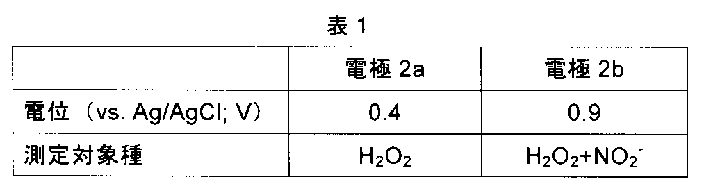
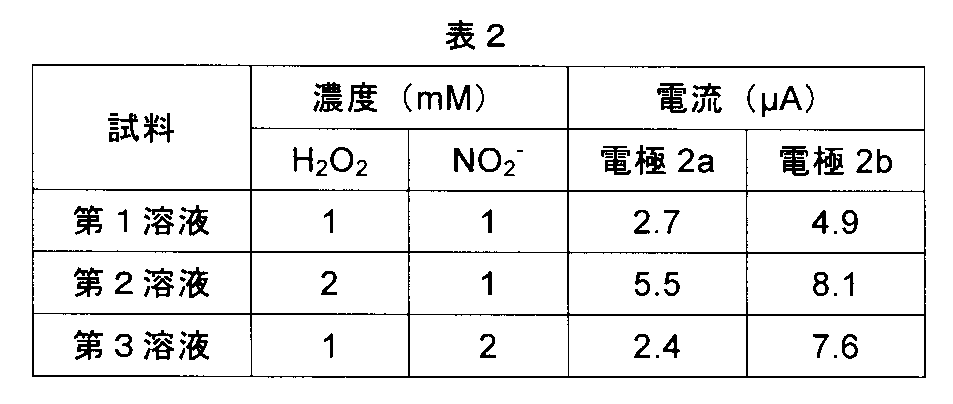
図42は、本発明の例3に係る生体センサの製造における一工程を概略的に示す平面図。図43は、図42に示す構造のXLIII-XLIII線に沿った断面図である。図44は、本発明の例3に係る生体センサの製造における一工程を概略的に示す斜視図である。本例では、以下に説明する方法により、生体センサを製造し、この生体センサを用いた測定を行った。
厚さ0.3mmのステンレス(SUS304)を加工して、図42及び42に示す金属板20を得た。この加工は、具体的には、以下の方法により行った。先ず、ステンレス板の両面へ感光性エッチングレジストを塗布した。これらレジスト層をパターン露光し、現像することにより、ステンレス板の両面にレジストパターンを形成した。次いで、これらレジストパターンをエッチングマスクとして用いて、ステンレスをエッチングした。エッチング液としては、塩化第2鉄溶液を使用した。その後、レジストパターンを剥離することにより、スリット27を有する金属板20を得た。次いで、基体21が金属板20に対して部分的に持ちあがるように、曲げ加工を行った。ここでは、基体21の長さは8mmとし、基体21は支持部25に対して2mm持ち上げた。
次に、金属板20の表面全体に、めっき法により、炭素からなる厚さ3μmの連続膜を、図33A乃至33Cなどに示す保護層22として形成した。具体的には、保護層22は、カルシウムカーバイドを含む溶融塩(LiCl-KCl-CaCl2:500℃)に金属板20を浸漬させ、アノード分極することによって形成した。
次に、図示しない金型のキャビティ内に、保護層22を形成した金属板20を設置した。次いで、金型に樹脂を射出し、この樹脂を硬化させた。これにより、図44に示す構造を得た。なお、この成形は、基体21のうち、電極2a及び2bに利用する部分と、後述する引き出し線と接続する部分とが、それぞれ、樹脂からなる支持体35の表面と裏面とから突き出るように行った。
次に、ダイシング装置によって、図44に示す構造をY-Y線に沿って切断して、主面の寸法が5mm×5mmの構造体を得た。これにより、支持部25から電極2a及び2bを分離した。
図19に示すプリント配線板PWBを準備した。このプリント配線板PWB上に、信号処理部4a及び出力部4cとしての半導体モジュールと、電源部4dとしての半導体モジュールとを搭載した。これにより、電子部品4を得た。
電子部品4の信号処理部4aに、これにデータ入力をするためのインターフェイス41と、引き出し線6a及び6bとを電気的に接続した。また、電子部品4の出力部4cに、ここから外部へとデータを受け渡すためのインターフェイス42を電気的に接続した。更に、電子部品4の電源部4dに、外部電源5を電気的に接続した。以上のようにして、図19に示す生体センサ1を完成した。
10μLの血液と、グルコースオキシターゼ及びフェリシアン化イオンを各々0.01mol/Lの濃度で含有した10μLの生理食塩水とを混合し、この混合液をプレパラート上に滴下した。混合を開始してから1分後に、この混合液の上から電極部2を押し当て、電極2a及び2b間に0.5Vの電圧を印加した。そして、電圧の印加を開始してから10秒後に電極2a及び2b間に流れる電流を測定した。この測定によって得られた電流値は、血中グルコース濃度が10乃至500mg/dLの範囲で1乃至10μAであり、血中グルコース濃度に対して高い線形性を示した。なお、この測定手法自体は、血中グルコース濃度の検出法として比較的一般的である。上記の試験により、上述した生体センサ1を用いた場合においても、正確な測定が可能であることが分かった。
Claims (14)
- 2以上の電極と、前記2以上の電極を支持した支持体とを具備し、
前記電極の1以上は、金属からなる表面を有している基体と、前記表面の少なくとも一部を被覆した保護層とを含み、
前記保護層は、炭素からなり且つ1μm以上の厚さを有している連続膜である生体センサ。 - 前記保護層は、前記表面のうち、少なくとも測定対象が接触し得る領域全体を被覆している請求項1に記載の生体センサ。
- 一端が前記表面に接合された引き出し線を更に具備し、前記保護層は、前記表面と前記引き出し線との接合部を除く、前記表面の全体を被覆している請求項1又は2に記載の生体センサ。
- 前記基体は、湾曲又は屈曲した形状を有しており、前記保護層は、前記表面のうち、少なくとも前記基体が湾曲又は屈曲した部分に対応した領域を被覆している請求項1乃至3の何れか1項に記載の生体センサ。
- 前記基体は、互いに平行な第1及び第2主面と、それらの縁に沿って延びた端面とを有し、前記保護層は、前記第1主面の全体と、前記第2主面の少なくとも一部と、前記端面の少なくとも一部とを被覆している請求項1乃至4の何れか1項に記載の生体センサ。
- 前記支持体は、前記2以上の電極を互いに対して傾くように支持した請求項5に記載の生体センサ。
- 前記基体は、コイル形状又は板ばね形状を有している請求項1乃至4の何れか1項に記載の生体センサ。
- 前記2以上の電極に電気的に接続され、それら電極間を流れる電流又はそれら電極間の電圧から、測定対象に関する情報を生成する処理部を更に具備した請求項1乃至7の何れか1項に記載の生体センサ。
- 前記情報を前記生体センサの外部へと出力する出力部を更に具備した請求項8に記載の生体センサ。
- 金属からなる表面を有している基体に、めっき法によって、炭素からなる保護層を、前記表面の少なくとも一部を被覆し且つ1μm以上の厚さを有するように形成して、電極を得る工程と、
前記電極を含む2以上の電極を支持体に支持させる工程と
を含んだ生体センサの製造方法。 - 前記電極を得る工程に先立ち、前記基体を変形させる工程を更に含んだ請求項10に記載の生体センサの製造方法。
- 前記金属からなる表面を有している板の一部を除去して、前記基体とこれに繋がった支持部とを含んだ構造体を得る工程と、
前記電極を得る工程の後に、前記基体を前記支持部から切り離す工程と
を更に含んだ請求項10又は11に記載の生体センサの製造方法。 - 前記基体のうち前記支持部から切り離すことにより剥き出しになった部分に引き出し線を接合することを更に含んだ請求項12に記載の生体センサの製造方法。
- 前記保護層の一部を除去して、前記表面の一部を剥き出しにさせ、この剥き出しになった部分に引き出し線を接合することを更に含んだ請求項12に記載の生体センサの製造方法。
Priority Applications (4)
| Application Number | Priority Date | Filing Date | Title |
|---|---|---|---|
| JP2017551950A JP6806079B2 (ja) | 2015-11-20 | 2016-11-18 | 生体センサ及びその製造方法 |
| EP16866445.6A EP3378393A4 (en) | 2015-11-20 | 2016-11-18 | BIOSENSOR AND MANUFACTURING METHOD THEREFOR |
| KR1020187017372A KR20180085760A (ko) | 2015-11-20 | 2016-11-18 | 생체 센서 및 그 제조 방법 |
| US15/951,531 US20180228396A1 (en) | 2015-11-20 | 2018-04-12 | Biosensor and a manufacturing method therefor |
Applications Claiming Priority (2)
| Application Number | Priority Date | Filing Date | Title |
|---|---|---|---|
| JP2015227645 | 2015-11-20 | ||
| JP2015-227645 | 2015-11-20 |
Related Child Applications (1)
| Application Number | Title | Priority Date | Filing Date |
|---|---|---|---|
| US15/951,531 Continuation US20180228396A1 (en) | 2015-11-20 | 2018-04-12 | Biosensor and a manufacturing method therefor |
Publications (1)
| Publication Number | Publication Date |
|---|---|
| WO2017086445A1 true WO2017086445A1 (ja) | 2017-05-26 |
Family
ID=58717440
Family Applications (1)
| Application Number | Title | Priority Date | Filing Date |
|---|---|---|---|
| PCT/JP2016/084286 Ceased WO2017086445A1 (ja) | 2015-11-20 | 2016-11-18 | 生体センサ及びその製造方法 |
Country Status (5)
| Country | Link |
|---|---|
| US (1) | US20180228396A1 (ja) |
| EP (1) | EP3378393A4 (ja) |
| JP (1) | JP6806079B2 (ja) |
| KR (1) | KR20180085760A (ja) |
| WO (1) | WO2017086445A1 (ja) |
Cited By (1)
| Publication number | Priority date | Publication date | Assignee | Title |
|---|---|---|---|---|
| JP2019184390A (ja) * | 2018-04-09 | 2019-10-24 | 凸版印刷株式会社 | 電気化学センサ用電極チップ及びその製造方法 |
Families Citing this family (5)
| Publication number | Priority date | Publication date | Assignee | Title |
|---|---|---|---|---|
| GB201701529D0 (en) * | 2017-01-31 | 2017-03-15 | Element Six Tech Ltd | Diamond based electrochemical sensors |
| CN111246797B (zh) | 2017-10-24 | 2025-09-09 | 德克斯康公司 | 预连接分析物传感器 |
| WO2019181643A1 (ja) * | 2018-03-20 | 2019-09-26 | 国立大学法人東北大学 | 飲み込みセンサ装置およびその製造方法 |
| US20200187793A1 (en) * | 2018-12-18 | 2020-06-18 | Movano Inc. | Systems for radio wave based health monitoring that utilize data derived from amplitude and/or phase data |
| CN113223827B (zh) * | 2021-04-21 | 2025-08-19 | 昆山玛冀电子有限公司 | 电感器及其制作方法 |
Citations (12)
| Publication number | Priority date | Publication date | Assignee | Title |
|---|---|---|---|---|
| JPS59128443A (ja) * | 1983-01-14 | 1984-07-24 | Matsushita Electric Works Ltd | バイオセンサ |
| JPH06148124A (ja) | 1992-11-12 | 1994-05-27 | Hitachi Ltd | ディスポーザブルイオンセンサユニット |
| WO1999045387A2 (en) | 1998-03-04 | 1999-09-10 | Therasense, Inc. | Electrochemical analyte sensor |
| JP2002207037A (ja) | 2000-11-10 | 2002-07-26 | Yoshitaka Otomo | 酸化還元電位測定機能を具備する健康管理計及び利用方法 |
| JP2006169554A (ja) | 2004-12-13 | 2006-06-29 | Doshisha | 炭素質皮膜及びその製造方法 |
| JP2007003256A (ja) | 2005-06-22 | 2007-01-11 | Techno Medica Co Ltd | 腎臓機能コントロール状態測定方法及び測定システム |
| JP2009120860A (ja) | 2007-11-12 | 2009-06-04 | Doshisha | 炭素膜の製造方法 |
| WO2009072645A1 (ja) * | 2007-12-07 | 2009-06-11 | Omron Corporation | 分析チップ |
| WO2010004690A1 (ja) | 2008-07-09 | 2010-01-14 | 日本電気株式会社 | 炭素電極、電気化学センサ、および炭素電極の製造方法 |
| JP2012101092A (ja) | 1997-02-06 | 2012-05-31 | Abbott Diabetes Care Inc | 小体積インビトロ被検体センサー |
| WO2013016573A1 (en) | 2011-07-26 | 2013-01-31 | Glysens Incorporated | Tissue implantable sensor with hermetically sealed housing |
| JP2013154010A (ja) * | 2012-01-31 | 2013-08-15 | Arkray Inc | 電気化学センサの製造方法、及び電気化学センサ |
Family Cites Families (3)
| Publication number | Priority date | Publication date | Assignee | Title |
|---|---|---|---|---|
| CA2616010C (en) * | 2005-07-20 | 2013-11-05 | Neil R. Euliano | Medication compliance system and associated methods |
| JP2009225934A (ja) * | 2008-03-21 | 2009-10-08 | Nitto Denko Corp | 体液採取用回路基板およびバイオセンサ |
| JP6159564B2 (ja) * | 2013-04-23 | 2017-07-05 | 田中貴金属工業株式会社 | センサー用電極およびその製造方法 |
-
2016
- 2016-11-18 EP EP16866445.6A patent/EP3378393A4/en not_active Withdrawn
- 2016-11-18 KR KR1020187017372A patent/KR20180085760A/ko not_active Withdrawn
- 2016-11-18 JP JP2017551950A patent/JP6806079B2/ja active Active
- 2016-11-18 WO PCT/JP2016/084286 patent/WO2017086445A1/ja not_active Ceased
-
2018
- 2018-04-12 US US15/951,531 patent/US20180228396A1/en not_active Abandoned
Patent Citations (12)
| Publication number | Priority date | Publication date | Assignee | Title |
|---|---|---|---|---|
| JPS59128443A (ja) * | 1983-01-14 | 1984-07-24 | Matsushita Electric Works Ltd | バイオセンサ |
| JPH06148124A (ja) | 1992-11-12 | 1994-05-27 | Hitachi Ltd | ディスポーザブルイオンセンサユニット |
| JP2012101092A (ja) | 1997-02-06 | 2012-05-31 | Abbott Diabetes Care Inc | 小体積インビトロ被検体センサー |
| WO1999045387A2 (en) | 1998-03-04 | 1999-09-10 | Therasense, Inc. | Electrochemical analyte sensor |
| JP2002207037A (ja) | 2000-11-10 | 2002-07-26 | Yoshitaka Otomo | 酸化還元電位測定機能を具備する健康管理計及び利用方法 |
| JP2006169554A (ja) | 2004-12-13 | 2006-06-29 | Doshisha | 炭素質皮膜及びその製造方法 |
| JP2007003256A (ja) | 2005-06-22 | 2007-01-11 | Techno Medica Co Ltd | 腎臓機能コントロール状態測定方法及び測定システム |
| JP2009120860A (ja) | 2007-11-12 | 2009-06-04 | Doshisha | 炭素膜の製造方法 |
| WO2009072645A1 (ja) * | 2007-12-07 | 2009-06-11 | Omron Corporation | 分析チップ |
| WO2010004690A1 (ja) | 2008-07-09 | 2010-01-14 | 日本電気株式会社 | 炭素電極、電気化学センサ、および炭素電極の製造方法 |
| WO2013016573A1 (en) | 2011-07-26 | 2013-01-31 | Glysens Incorporated | Tissue implantable sensor with hermetically sealed housing |
| JP2013154010A (ja) * | 2012-01-31 | 2013-08-15 | Arkray Inc | 電気化学センサの製造方法、及び電気化学センサ |
Non-Patent Citations (2)
| Title |
|---|
| See also references of EP3378393A4 |
| Y. LI ET AL., ELECTROCHIMICA ACTA, vol. 144, 2014, pages 111 - 118 |
Cited By (2)
| Publication number | Priority date | Publication date | Assignee | Title |
|---|---|---|---|---|
| JP2019184390A (ja) * | 2018-04-09 | 2019-10-24 | 凸版印刷株式会社 | 電気化学センサ用電極チップ及びその製造方法 |
| JP7127339B2 (ja) | 2018-04-09 | 2022-08-30 | 凸版印刷株式会社 | 電気化学センサ用電極チップ及びその製造方法 |
Also Published As
| Publication number | Publication date |
|---|---|
| KR20180085760A (ko) | 2018-07-27 |
| EP3378393A4 (en) | 2019-08-14 |
| EP3378393A1 (en) | 2018-09-26 |
| US20180228396A1 (en) | 2018-08-16 |
| JP6806079B2 (ja) | 2021-01-06 |
| JPWO2017086445A1 (ja) | 2018-09-13 |
Similar Documents
| Publication | Publication Date | Title |
|---|---|---|
| JP6806079B2 (ja) | 生体センサ及びその製造方法 | |
| Li et al. | Microneedle-based potentiometric sensing system for continuous monitoring of multiple electrolytes in skin interstitial fluids | |
| US20240148280A1 (en) | Implantable micro-biosensor and method for manufacturing the same | |
| Zhai et al. | Vertically aligned gold nanowires as stretchable and wearable epidermal ion-selective electrode for noninvasive multiplexed sweat analysis | |
| JP4797024B2 (ja) | 導管なし埋め込み式針状生物センサー | |
| US5954685A (en) | Electrochemical sensor with dual purpose electrode | |
| US12364418B2 (en) | Method for manufacturing implantable micro-biosensor | |
| Gil et al. | Smart implanted access port catheter for therapy intervention with pH and lactate biosensors | |
| US10016154B2 (en) | Placeable sensor and method of using same | |
| CN118924292A (zh) | 一种用于监测汗液尿酸浓度的可穿戴传感装置 | |
| Huang et al. | Semi-implantable device based on multiplexed microfilament electrode cluster for continuous monitoring of physiological ions | |
| JP2018096875A (ja) | 生体センサ、生体センサの製造方法及びバイオセンシング装置 | |
| JP6844238B2 (ja) | 生体センサのための電極および生体センサ | |
| CN119498833B (zh) | 分析物监测方法、可读存储介质及分析物监测系统 | |
| JP3946516B2 (ja) | 生体情報測定用装置及び生体情報測定用センサ | |
| Wang et al. | PCB-Based Mass-Produced EGFET pH Sensor with Electroplated Reference Electrode for Daily Saliva Acidity Monitoring in Mouth | |
| CA3104900C (en) | Implantable micro-biosensor and method for operating the same | |
| US20200129105A1 (en) | Physiological characteristic sensors and methods for making and operating such sensors | |
| WO2026080785A2 (en) | Determining conditions impacting analyte sensor performance | |
| CN104684476A (zh) | 用于制造传感器仪器的方法和传感器仪器 |
Legal Events
| Date | Code | Title | Description |
|---|---|---|---|
| 121 | Ep: the epo has been informed by wipo that ep was designated in this application |
Ref document number: 16866445 Country of ref document: EP Kind code of ref document: A1 |
|
| ENP | Entry into the national phase |
Ref document number: 2017551950 Country of ref document: JP Kind code of ref document: A |
|
| NENP | Non-entry into the national phase |
Ref country code: DE |
|
| ENP | Entry into the national phase |
Ref document number: 20187017372 Country of ref document: KR Kind code of ref document: A |
|
| WWE | Wipo information: entry into national phase |
Ref document number: 1020187017372 Country of ref document: KR |
|
| WWE | Wipo information: entry into national phase |
Ref document number: 2016866445 Country of ref document: EP |