WO2017094814A1 - 電子部品収容機器および電子装置 - Google Patents
電子部品収容機器および電子装置 Download PDFInfo
- Publication number
- WO2017094814A1 WO2017094814A1 PCT/JP2016/085669 JP2016085669W WO2017094814A1 WO 2017094814 A1 WO2017094814 A1 WO 2017094814A1 JP 2016085669 W JP2016085669 W JP 2016085669W WO 2017094814 A1 WO2017094814 A1 WO 2017094814A1
- Authority
- WO
- WIPO (PCT)
- Prior art keywords
- electronic component
- housing
- bottom plate
- heat
- partition plate
- Prior art date
- Legal status (The legal status is an assumption and is not a legal conclusion. Google has not performed a legal analysis and makes no representation as to the accuracy of the status listed.)
- Ceased
Links
Images




Classifications
-
- H—ELECTRICITY
- H05—ELECTRIC TECHNIQUES NOT OTHERWISE PROVIDED FOR
- H05K—PRINTED CIRCUITS; CASINGS OR CONSTRUCTIONAL DETAILS OF ELECTRIC APPARATUS; MANUFACTURE OF ASSEMBLAGES OF ELECTRICAL COMPONENTS
- H05K7/00—Constructional details common to different types of electric apparatus
- H05K7/20—Modifications to facilitate cooling, ventilating, or heating
- H05K7/2039—Modifications to facilitate cooling, ventilating, or heating characterised by the heat transfer by conduction from the heat generating element to a dissipating body
-
- H—ELECTRICITY
- H05—ELECTRIC TECHNIQUES NOT OTHERWISE PROVIDED FOR
- H05K—PRINTED CIRCUITS; CASINGS OR CONSTRUCTIONAL DETAILS OF ELECTRIC APPARATUS; MANUFACTURE OF ASSEMBLAGES OF ELECTRICAL COMPONENTS
- H05K7/00—Constructional details common to different types of electric apparatus
- H05K7/20—Modifications to facilitate cooling, ventilating, or heating
- H05K7/2039—Modifications to facilitate cooling, ventilating, or heating characterised by the heat transfer by conduction from the heat generating element to a dissipating body
- H05K7/20436—Inner thermal coupling elements in heat dissipating housings, e.g. protrusions or depressions integrally formed in the housing
- H05K7/20445—Inner thermal coupling elements in heat dissipating housings, e.g. protrusions or depressions integrally formed in the housing the coupling element being an additional piece, e.g. thermal standoff
-
- H—ELECTRICITY
- H05—ELECTRIC TECHNIQUES NOT OTHERWISE PROVIDED FOR
- H05K—PRINTED CIRCUITS; CASINGS OR CONSTRUCTIONAL DETAILS OF ELECTRIC APPARATUS; MANUFACTURE OF ASSEMBLAGES OF ELECTRICAL COMPONENTS
- H05K5/00—Casings, cabinets or drawers for electric apparatus
- H05K5/02—Details
- H05K5/0217—Mechanical details of casings
-
- H—ELECTRICITY
- H05—ELECTRIC TECHNIQUES NOT OTHERWISE PROVIDED FOR
- H05K—PRINTED CIRCUITS; CASINGS OR CONSTRUCTIONAL DETAILS OF ELECTRIC APPARATUS; MANUFACTURE OF ASSEMBLAGES OF ELECTRICAL COMPONENTS
- H05K7/00—Constructional details common to different types of electric apparatus
- H05K7/20—Modifications to facilitate cooling, ventilating, or heating
-
- H—ELECTRICITY
- H05—ELECTRIC TECHNIQUES NOT OTHERWISE PROVIDED FOR
- H05K—PRINTED CIRCUITS; CASINGS OR CONSTRUCTIONAL DETAILS OF ELECTRIC APPARATUS; MANUFACTURE OF ASSEMBLAGES OF ELECTRICAL COMPONENTS
- H05K7/00—Constructional details common to different types of electric apparatus
- H05K7/20—Modifications to facilitate cooling, ventilating, or heating
- H05K7/20009—Modifications to facilitate cooling, ventilating, or heating using a gaseous coolant in electronic enclosures
- H05K7/20136—Forced ventilation, e.g. by fans
- H05K7/20145—Means for directing air flow, e.g. ducts, deflectors, plenum or guides
-
- H—ELECTRICITY
- H05—ELECTRIC TECHNIQUES NOT OTHERWISE PROVIDED FOR
- H05K—PRINTED CIRCUITS; CASINGS OR CONSTRUCTIONAL DETAILS OF ELECTRIC APPARATUS; MANUFACTURE OF ASSEMBLAGES OF ELECTRICAL COMPONENTS
- H05K7/00—Constructional details common to different types of electric apparatus
- H05K7/20—Modifications to facilitate cooling, ventilating, or heating
- H05K7/2089—Modifications to facilitate cooling, ventilating, or heating for power electronics, e.g. for inverters for controlling motor
- H05K7/209—Heat transfer by conduction from internal heat source to heat radiating structure
-
- H—ELECTRICITY
- H05—ELECTRIC TECHNIQUES NOT OTHERWISE PROVIDED FOR
- H05K—PRINTED CIRCUITS; CASINGS OR CONSTRUCTIONAL DETAILS OF ELECTRIC APPARATUS; MANUFACTURE OF ASSEMBLAGES OF ELECTRICAL COMPONENTS
- H05K7/00—Constructional details common to different types of electric apparatus
- H05K7/20—Modifications to facilitate cooling, ventilating, or heating
- H05K7/2089—Modifications to facilitate cooling, ventilating, or heating for power electronics, e.g. for inverters for controlling motor
- H05K7/20909—Forced ventilation, e.g. on heat dissipaters coupled to components
-
- H—ELECTRICITY
- H05—ELECTRIC TECHNIQUES NOT OTHERWISE PROVIDED FOR
- H05K—PRINTED CIRCUITS; CASINGS OR CONSTRUCTIONAL DETAILS OF ELECTRIC APPARATUS; MANUFACTURE OF ASSEMBLAGES OF ELECTRICAL COMPONENTS
- H05K5/00—Casings, cabinets or drawers for electric apparatus
- H05K5/02—Details
- H05K5/0217—Mechanical details of casings
- H05K5/023—Handles; Grips
-
- H—ELECTRICITY
- H05—ELECTRIC TECHNIQUES NOT OTHERWISE PROVIDED FOR
- H05K—PRINTED CIRCUITS; CASINGS OR CONSTRUCTIONAL DETAILS OF ELECTRIC APPARATUS; MANUFACTURE OF ASSEMBLAGES OF ELECTRICAL COMPONENTS
- H05K5/00—Casings, cabinets or drawers for electric apparatus
- H05K5/04—Metal casings
-
- H—ELECTRICITY
- H05—ELECTRIC TECHNIQUES NOT OTHERWISE PROVIDED FOR
- H05K—PRINTED CIRCUITS; CASINGS OR CONSTRUCTIONAL DETAILS OF ELECTRIC APPARATUS; MANUFACTURE OF ASSEMBLAGES OF ELECTRICAL COMPONENTS
- H05K7/00—Constructional details common to different types of electric apparatus
- H05K7/20—Modifications to facilitate cooling, ventilating, or heating
- H05K7/20009—Modifications to facilitate cooling, ventilating, or heating using a gaseous coolant in electronic enclosures
- H05K7/20136—Forced ventilation, e.g. by fans
- H05K7/20172—Fan mounting or fan specifications
Definitions
- the present invention relates to an electronic component housing device or the like, for example, an electronic component housing device or the like that houses an electronic component that generates heat.
- the microwave power module (MPM: Microwave Power Module) is an amplification module used in microwave band communication.
- a typical microwave power module has a TWT (traveling wave tube: Traveling Electro Wave Tube) and an EPC (Electronic Power Conditioner).
- EPC is also called a high voltage power supply module.
- TWT outputs power ranging from several tens of watts (watts) to several kW (kilowatts). For this reason, TWT generates high temperature heat as a heating element.
- Patent Document 1 Technology for dissipating heat from a heating element such as TWT is disclosed in Patent Document 1 and Patent Document 2, for example.
- Patent Document 1 discloses a technique for dissipating heat from a heating element (electrode structure) using a heat sink.
- the heat sink receives the heat of the heating element via the insulating member.
- the heat sink dissipates the received heat.
- it is possible to suppress the temperature rise of the heating element by radiating the heat of the heating element with the heat sink.
- Patent Document 2 discloses that the heat of a heating element (an electronic component with a large amount of heat generation (for example, a power amplification unit, a power supply unit)) does not affect other modules (electronic components with a small amount of heat generation).
- a technique for dissipating heat is disclosed.
- the partition plate is provided between the high heat generating module housing portion that houses the heat generating element and the low heat generating module housing portion that houses other modules. By providing the partition plate, it is reduced that the heat of the heating element affects other modules. Thereby, the temperature rise of another module can be suppressed.
- the housing that houses the heating element sometimes functions as a heat conductor.
- the heat of the electronic component having a large heat generation amount may be applied to the electronic component having a small heat generation amount through the housing.
- a metal for example, aluminum or iron
- metal is widely used as a material for a housing of a general microwave power module because it is easy to process and has a high strength. Since metal has a high thermal conductivity, the housing itself can be a path for heat conduction. Therefore, in the microwave power module, in particular, the possibility that the heat of the electronic component having a large calorific value is applied to the electronic component having a small calorific value through the housing is increased.
- the heat of the heat generating body accommodated in the high heat generating module accommodating portion is reduced by providing the partition plate to reduce the influence of the heat of the heat generating element on other modules.
- it may occur when added to another module housed in the low heat generating module housing portion via the partition plate.
- This invention is made
- An object of the present invention is to provide an electronic component housing device or the like that can efficiently cool the heat of the second electronic component while suppressing the above.
- An electronic component housing device includes a first electronic component, a housing that houses a second electronic component that generates a larger amount of heat than the first electronic component, and a first housing that houses the first electronic component. Between the first electronic component storage chamber, the second electronic component storage chamber, the second electronic component storage chamber, the second electronic component storage chamber, and the second electronic component storage chamber. Between the first partition plate disposed on the first electronic component housing chamber side, the first electronic component housing chamber and the second electronic component housing chamber, and the second electronic device component The second partition plate disposed on the storage chamber side, the first partition plate, and the second partition plate are provided so as to face each other at least partially, and the first partition plate and the second partition plate are provided. A first gap is provided between the plates.
- An electronic device of the present invention includes a first electronic component, a second electronic component that generates a larger amount of heat than the first electronic component, and a housing that houses the first electronic component and the second electronic component.
- a first electronic component storage chamber for storing the first electronic component a second electronic component storage chamber for storing the second electronic component, the first electronic component storage chamber, and the second electronic component storage chamber.
- the second partition plate disposed on the second electronic component housing chamber side, the first partition plate and the second partition plate are provided to face each other at least partially, A first gap is provided between the first partition plate and the second partition plate.
- the second electronic component is suppressed while the heat of the second electronic component having a larger calorific value than the first electronic component is suppressed from being applied to the first electronic component. Can be efficiently cooled.
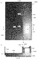
- FIG. 7A is a top view showing a simulation result of heat dissipation of the electronic device according to the second embodiment of the present invention.
- FIG. 7B is a cross-sectional view showing a heat dissipation simulation result of the electronic device according to the second embodiment of the present invention, and is a cross-sectional view taken along the line AA in FIG.
- FIG. 8A is a top view showing a heat radiation simulation result of a comparative example of the electronic device according to the second embodiment of the present invention.
- FIG. 8B is a cross-sectional view showing a heat radiation simulation result of the comparative example of the electronic device according to the second embodiment of the present invention, and is a cross-sectional view taken along the line BB in FIG. 8A. . It is a figure which shows the thermal radiation simulation result of the electronic device in the 2nd Embodiment of this invention.
- FIG. 9A is a top view illustrating a heat radiation simulation result of the electronic device according to the second embodiment of the present invention.
- FIG. 9B is a cross-sectional view showing a heat dissipation simulation result of the electronic device according to the second embodiment of the present invention, and is a cross-sectional view taken along the line CC in FIG. 9A.
- FIG. 10A is a top view showing a heat radiation simulation result of a modification of the electronic device according to the second embodiment of the present invention.
- FIG. 10B is a cross-sectional view showing a heat radiation simulation result of a modification of the electronic device according to the second embodiment of the present invention, and is a cross-sectional view taken along the line DD in FIG.
- It is a perspective view which shows the internal structure of the electronic device in the 3rd Embodiment of this invention.
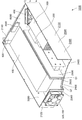
- FIG. 1 is a perspective view showing an internal configuration of the electronic apparatus 1000.
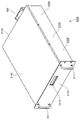
- FIG. 2 is a perspective view of the external appearance of the electronic apparatus 1000 viewed from the front side.
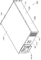
- FIG. 3 is a perspective view of the external appearance of the electronic apparatus 1000 viewed from the back side.
- FIG. 4 is a top view showing an internal configuration of the electronic apparatus 1000.
- FIG. 5 is a perspective view showing an internal configuration of the electronic component housing device 2000.
- the electronic device 1000 is, for example, a microwave power module.
- the microwave power module is a relatively new module that combines the features of high power and high efficiency achieved by TWT with the small size, high gain and low noise of SSA (Solid State Amplifier). Yes.
- the electronic device 1000 is described as a microwave power module.
- the electronic device 1000 is mounted on, for example, a satellite communication device or a medical device.
- the electronic apparatus 1000 includes a high voltage power supply module 100, a TWT 200, a heat sink 300, a first fan unit 400, a second fan unit 500, and a control module 600.
- the inlet 700, the outlet 800, and the electronic component housing device 2000 are provided.
- the high voltage power supply module 100 is the first electronic component of the present invention.
- TWT 200 is the second electronic component of the present invention.
- a passive element such as a resistor, a capacitor, or a piezoelectric element may be provided as the first component.
- a cable, a connector, or the like may be provided as the first component.
- the electronic component housing device 2000 includes a housing 2100, a first bottom plate 2300, a second bottom plate 2400, a first partition plate 2500, and a second partition plate. 2600.
- the housing 2100 houses the high-voltage power supply module 100, the TWT 200, the heat sink 300, the first fan unit 400, the second fan unit 500, and the control module 600.
- the material of the housing 2100 for example, the strength, weight and heat dissipation of the housing 2100, the influence of magnetism on the TWT 200, and the like are considered.
- a metal such as aluminum is used as the material of the housing 2100.
- the thermal conductivity of aluminum is about 236 (W / mK), which is higher than the thermal conductivity of iron (84 (W / mK)).
- the housing 2100 is formed in a box shape.
- the housing 2100 includes a front plate 2110, a back plate 2120, a body portion 2130, and an upper cover 2140.
- the front plate 2110 is formed in a plate shape. Front plate 2110 is attached to body portion 2130 by welding or screwing. As shown in FIG. 2, a pair of handles 2111 are attached to the front plate 2110. An opening window 2112 is formed on the front plate 2110. For example, a display screen of a liquid crystal panel (not shown) indicating the control state of the control module 600 is attached to the opening window 2112.
- the back plate 2120 is formed in a plate shape.
- the back plate 2120 is attached to the body portion 2130 by welding or screwing.
- An inlet 700 and an outlet 800 are formed in the back plate 2120.
- the second fan unit 500 is attached to the inflow port 700.
- the waveguide 900 is attached to the back plate 2120.
- the body portion 2130 is formed in the shape of a letter “U” or an alphabetical character in a cut surface obtained by cutting the housing 2100 along a plane perpendicular to the extending direction of the first partition plate 2500 and the second partition plate 2600. It is formed in a “U” shape.
- the body portion 2130 has the first bottom surface 2300 and the second bottom surface 2400 described above.
- the front plate 2110 and the back plate 2120 are attached to the body portion 2130 by welding or screwing.
- the upper cover 2140 is formed in a plate shape.
- the upper cover 2140 covers the body 2130 to which the front plate 2110 and the back plate 2120 are attached from the upper side.
- the upper cover 2140 is attached to the front plate 2110, the back plate 2120, and the body portion 2130 by screwing or the like. As a result, the inside of the housing 2100 is closed.
- the inside of the housing 2100 is divided into a first electronic component storage chamber 5000 and a second electronic device by a first partition plate 2500 and a second partition plate 2600. It is divided into a parts storage chamber 6000.
- the first electronic component storage chamber 5000 stores at least the high voltage power supply module 100.
- Second electronic component storage chamber 6000 stores at least TWT 200.
- the communication unit 7000 is provided between the first electronic component storage chamber 5000 and the second electronic component storage chamber 6000.
- the communication unit 7000 communicates between the first electronic component storage chamber 5000 and the second electronic component storage chamber 6000. Thereby, air can go back and forth between the first electronic component storage chamber 5000 and the second electronic component storage chamber 6000 via the communication portion 7000.
- the communication part 7000 does not need to be provided.
- the first bottom plate 2300 is formed on the body portion 2130. That is, the first bottom plate 2300 is a part of the housing 2100. Further, as shown in FIGS. 1 and 4, the high voltage power supply module 100 is installed on the first bottom plate 2300 and is thermally connected to the first bottom plate 2300. Thereby, the heat of the high voltage power supply module 100 is transferred to the first bottom plate 2300.
- the second bottom plate 2400 is formed on the body portion 2130. That is, the second bottom plate 2400 is a part of the housing 2100. As shown in FIGS. 1 and 4, the TWT 200 is installed on the second bottom plate 2400 and is thermally connected to the second bottom plate 2400. Thereby, the heat of TWT 200 is transferred to second bottom plate 2400.
- the first partition plate 2500 is attached to the body portion 2130. That is, the first partition plate 2500 is a part of the housing 2100. More specifically, as shown in FIG. 1, the first partition plate 2500 is attached to the first bottom plate 2300. Further, the first partition plate 2500 is thermally connected to the first bottom plate 2300. As shown in FIG. 1 and FIG. 4, the first partition plate 2500 is between the first electronic component storage chamber 5000 and the second electronic component storage chamber 6000 and is in the first electronic component storage chamber. It is arranged on the 5000 side.
- the second partition plate 2600 is attached to the body portion 2130. That is, the second partition plate 2600 is a part of the housing 2100. More specifically, as shown in FIG. 1, the second partition plate 2600 is attached to the second bottom plate 2400. The second partition plate 2600 is thermally connected to the second bottom plate 2400. As shown in FIGS. 1 and 4, the second partition plate 2600 is between the first electronic component storage chamber 5000 and the second electronic component storage chamber 6000, and is in the second electronic component storage chamber. It is arranged on the 6000 side.
- the first partition plate 2500 and the second partition plate 2600 are provided so as to face each other at least partially.
- a first gap G ⁇ b> 1 is provided between the first partition plate 2500 and the second partition plate 2600. That is, the first partition plate 2500 and the second partition plate 2600 are not directly thermally connected to each other.
- a second gap G ⁇ b> 2 is provided between the first bottom plate 2300 and the second bottom plate 2400. That is, the first bottom plate 2300 and the second bottom plate 2400 are not directly thermally connected to each other.
- the configuration of the electronic component housing device 2000 has been described above.
- the high voltage power supply module 100 is accommodated in the first electronic component accommodating chamber 5000.
- the high voltage power supply module 100 is installed on the first bottom plate 2300 and is thermally connected to the first bottom plate 2300.
- the high-voltage power supply module 100 supplies power to drive each electronic component such as the TWT 200, the first fan unit 400, the second fan unit 500, and the control module 600.
- the general high-voltage power supply module 100 uses a lot of semiconductors, and therefore a certain level of heat countermeasures are taken.
- the TWT 200 is housed in the second electronic component housing chamber 6000. Further, the TWT 200 is installed on the second bottom plate 2400 and is thermally connected to the second bottom plate 2400.
- the TWT 200 amplifies and outputs a high frequency signal.
- the TWT 200 amplifies a high frequency signal using an electron beam (not shown) emitted by an electron gun (not shown).
- the TWT 200 has a larger output power and a larger amount of heat generation than other electronic components such as the high-voltage power supply module 100. That is, the TWT 200 consumes a larger amount of power than other electronic components.
- the TWT 200 is a device having a higher power density than other electronic components.
- the TWT 200 may use a high voltage on the order of kilovolts, for example.
- the TWT 200 When a semiconductor is used for the microwave module, the output of the semiconductor rapidly decreases especially when the frequency increases. For this reason, the TWT 200 tends to be used for a microwave module, particularly when a high-frequency signal is handled. After a high frequency signal is amplified using TWT 200, 70-90% energy may remain in the electron beam. These energies are absorbed by the electrodes and the like. As a result, the TWT 200 generates heat higher than that of the high voltage power supply module 100.
- the TWT 200 is provided in the vicinity of the discharge port 800.
- the electronic apparatus 1000 can efficiently discharge the heat of the TWT 200 to the outside of the housing 2100 of the electronic component housing device 2000.
- the heat sink 300 is attached to the TWT 200.
- the heat sink 300 receives the heat of the TWT 200 and radiates it into the air.
- the first fan unit 400 is housed in the second electronic component housing chamber 6000. As shown in FIGS. 1 and 4, the first fan unit 400 is provided on the front plate 2110 side. As shown in FIG. 4, the first fan unit 400 causes the air flowing from the first electronic component storage chamber 5000 to the second electronic component storage chamber 6000 to the heat sink 300 via the communication unit 7000. Supply. As a result, the heat sink 300 that has received the heat of the TWT 200 is cooled.
- the second fan unit 500 is attached to the inlet 700 from the outside of the housing 2100.
- the second fan unit 500 facilitates air outside the housing 2100 (cooling air) to flow into the first electronic component housing chamber 5000 of the housing 2100.
- control module 600 is attached to the front plate 2110 from the inside of the housing 2100.
- the control module 600 controls other electronic components.
- the inlet 700 is formed in the back plate 2120.
- the inflow port 700 is formed on the first electronic component storage chamber 5000 side of the housing 2100. Air outside the housing 2100 flows into the first electronic component housing chamber 5000 of the housing 2100 through the inflow port 700.
- the discharge port 800 is formed in the back plate 2120.
- the discharge port 800 is formed on the second electronic component housing chamber 6000 side of the housing 2100. Air in the housing 2100 flows out of the housing 2100 through the outflow port 800.
- the waveguide 900 is provided on the back plate.
- the waveguide 900 outputs the high-frequency signal amplified by the TWT 200 to the outside of the housing 2100.
- the configuration of the electronic device 1000 has been described above.
- the high voltage power supply module 100 supplies power to electronic components such as the TWT 200, the first fan unit 400, the second fan unit 500, and the control module 600.
- electronic parts such as TWT200, the 1st fan part 400, the 2nd fan part 500, and control module 600, operate.
- the TWT 200, the high voltage power supply module 100, etc. generate heat.
- the heat sink 300 receives the heat of the TWT 200 and radiates it.
- the cooling operation of the electronic components in the housing 2100 a cooling operation by forced air cooling of the air in the housing 2100 and a cooling operation by heat conduction of the housing 2100 itself are adopted.
- the air outside the housing 2100 flows into the housing 2100 through the inflow port 700 due to the blowing of the second fan unit 500.
- the air outside the housing 2100 flows in the first first electronic component storage chamber 5000 while including the heat of the high voltage power supply module 100. In this way, the heat of the high voltage power supply module 100 is cooled by the air outside the housing 2100.
- the air flowing through the first electronic component housing chamber 5000 is blown by the first fan unit 400, and the second electronic component is transmitted via the communication unit 7000. It flows into the storage chamber 6000.
- the air that has passed through the communication unit 7000 flows to the heat sink 300 by the air blowing of the first fan unit 400.
- the heat sink 300 receives the heat of the TWT 200 and radiates it.
- the heat sink 300 is cooled. That is, the thermal energy of TWT 200 is absorbed by the air that has passed through communication portion 7000 via heat sink 300. Thereby, the heat of TWT200 is efficiently radiated.
- the air that has passed through the heat sink 300 further includes the heat of the TWT 200 and flows toward the discharge port 800, and as shown by the arrow f in FIG. It is discharged out of the body 2100.
- the air outside the housing 2100 is converted into the first electronic component storage chamber 5000 and the second electronic component in the housing 2100 by the first fan unit 400 and the second fan unit 500. It sequentially flows through the storage chamber 6000 and is discharged out of the housing 2100. During this time, the air flowing in the housing 2100 flows to the discharge port 800 while including the heat of the high voltage power supply module 100 and the TWT 200. Thereby, the heat of the high voltage power supply module 100 and the TWT 200 can be discharged out of the housing 2100.
- the high voltage power supply module 100 is installed on the first bottom plate 2300. For this reason, the heat of the high voltage power supply module 100 is transferred to the first bottom plate 2300. That is, the heat energy of the high voltage power supply module 100 is applied to the first bottom plate 2300. The heat of the high voltage power supply module 100 is also transferred to the first partition plate 2500 by the first bottom plate 2300. Thereby, the heat of the high voltage power supply module 100 is cooled by the heat received by the first bottom plate 2300 and the first partition plate 2500.
- the TWT 200 is installed on the second bottom plate 2400. For this reason, the heat of the TWT 200 is transferred to the second bottom plate 2400. That is, the thermal energy of the TWT 200 is applied to the second bottom plate 2400. The heat of the TWT 200 is also transferred to the second partition plate 2600 via the second bottom plate 2400. Thereby, the heat of TWT 200 is cooled by the heat received by second bottom plate 2400 and second partition plate 2600.
- the heat of the high voltage power supply module 100 is transferred to the first partition plate 2500 through the air in the first electronic component housing chamber 5000. Thereby, the heat of the high voltage power supply module 100 is cooled by the heat received by the first partition plate 2500.
- the heat of TWT 200 is transferred to second partition plate 2600 through the air in second electronic component housing chamber 6000. Thereby, the heat of TWT 200 is cooled by the heat received by second partition plate 2600.
- a first gap G1 is provided between the first partition plate 2500 and the second partition plate 2600. That is, the first partition plate 2500 and the second partition plate 2600 are separated from each other. For this reason, direct heat conduction between the first partition plate 2500 and the second partition plate 2600 does not occur. That is, direct transport of thermal energy due to heat conduction inside the first partition plate 2500 and the second partition plate 2600 does not occur between the first partition plate 2500 and the second partition plate 2600. That is, by providing the first gap G1 between the first partition plate 2500 and the second partition plate 2600, the space between the first electronic component storage chamber 5000 and the second electronic component storage chamber 6000 is reduced. Heat transfer can be suppressed.
- the heat of the TWT 200 that generates a larger amount of heat than the high voltage power supply module 100 is suppressed from being applied to the high voltage power supply module 100 via the first partition plate 2500 and the second partition plate 2600. Thereby, it can suppress that the temperature of the high voltage power supply module 100 rises with the heat of TWT200. Therefore, it can suppress that the performance of the high voltage power supply module 100 deteriorates with the heat
- the TWT 200 and the high voltage power supply module can be suppressed while suppressing the heat of the TWT 200 that generates a larger amount of heat than the high voltage power supply module 100 from being applied to the high voltage power supply module 100. 100 heat can be efficiently cooled.
- a second gap G2 is provided between the first bottom plate 2300 and the second bottom plate 2400. That is, the first bottom plate 2300 and the second bottom plate 2400 are separated from each other. For this reason, direct heat conduction between the first bottom plate 2300 and the second bottom plate 2400 does not occur. That is, direct transport of thermal energy due to heat conduction inside the first bottom plate 2300 and the second bottom plate 2400 does not occur between the first bottom plate 2300 and the second bottom plate 2400. That is, the heat of the TWT 200 that generates a larger amount of heat than the high voltage power supply module 100 is not applied to the high voltage power supply module 100 via the first bottom plate 2300 and the second bottom plate 2400.
- the high voltage power supply module 100 and the high voltage power supply module 100 can be prevented from applying heat to the high voltage power supply module 100 with the heat generation amount larger than that of the high voltage power supply module 100.
- the heat of the TWT 200 can be efficiently cooled.
- first gap G1 and the second gap G2 are in communication. For this reason, direct heat conduction between the first bottom plate 2300 and the second partition plate 2600 does not occur. That is, direct transport of thermal energy due to heat conduction inside the first bottom plate 2300 and the second partition plate 2600 does not occur between the first bottom plate 2300 and the second partition plate 2600. That is, the heat of the TWT 200 that generates a larger amount of heat than the high voltage power supply module 100 is not applied to the high voltage power supply module 100 via the first bottom plate 2300 and the second partition plate 2600. Further, direct heat conduction between the second bottom plate 2400 and the first partition plate 2500 does not occur.
- the first gap portion G1 and the second gap portion G2 communicate with each other, so that the heat of the TWT 200 that generates a larger amount of heat than the high voltage power supply module 100 is suppressed from being applied to the high voltage power supply module 100. Meanwhile, the heat of the TWT 200 and the high voltage power supply module 100 can be efficiently cooled.
- the electronic component housing device 2000 includes the housing 2100, the first electronic component housing chamber 5000, the second electronic component housing chamber 6000, and the first partition.
- a plate 2500 and a second partition plate 2600 are provided.
- the housing 2100 accommodates the high voltage power supply module 100 (first electronic component) and the TWT 200 (second electronic component) that generates a larger amount of heat than the high voltage power supply module 100.
- the first electronic component housing chamber 5000 houses the high voltage power supply module 100.
- Second electronic component storage chamber 6000 stores TWT 200.
- the first partition plate 2500 is disposed between the first electronic component storage chamber 5000 and the second electronic component storage chamber 6000 and on the first electronic component storage chamber 5000 side.
- the second partition plate 2600 is disposed between the first electronic component storage chamber 5000 and the second electronic component storage chamber 6000 and on the second electronic component storage chamber 6000 side.
- the first partition plate 2500 and the second partition plate 2600 are provided so as to face each other at least partially.
- a first gap G ⁇ b> 1 is provided between the first partition plate 2500 and the second partition plate 2600.
- the housing 2100 is used for the first electronic component housing chamber 5000 and the second electronic component housing chamber 6000 using the first partition plate 2500 and the second partition plate 2600. It is divided into.
- the first electronic component housing chamber 5000 houses the high voltage power supply module 100.
- Second electronic component storage chamber 6000 stores TWT 200. That is, in the electronic component housing device 2000, the first partition plate 2500 and the second partition plate 2600 are provided, and the high voltage power supply module 100 and the TWT 200 are housed in separate housing chambers. Thereby, it can suppress that the heat of TWT200 is added to the high voltage power supply module 100 via the air in the housing
- a first gap G1 is provided between the first partition plate 2500 and the second partition plate 2600. That is, the first partition plate 2500 and the second partition plate 2600 are separated from each other. For this reason, direct heat conduction between the first partition plate 2500 and the second partition plate 2600 does not occur. That is, by providing the first gap G1 between the first partition plate 2500 and the second partition plate 2600, the space between the first electronic component storage chamber 5000 and the second electronic component storage chamber 6000 is reduced. Direct movement of heat can be suppressed. Therefore, it is possible to suppress the heat of the TWT 200 having a larger calorific value than that of the high voltage power supply module 100 from being applied to the high voltage power supply module 100 via the first partition plate 2500 and the second partition plate 2600. Thereby, it can suppress that the temperature of the high voltage power supply module 100 rises with the heat of TWT200.
- the heat of the TWT 200 which generates a larger amount of heat than the high voltage power supply module 100, is prevented from being applied to the high voltage power supply module 100, and the heat of the TWT 200 is efficiently obtained. Can be cooled.
- the electronic component housing device 2000 includes a first bottom plate 2300 and a second bottom plate 2400.
- the first bottom plate 2300 is a part of the housing 2100, and the high voltage power supply module 100 (first electronic component) is installed and thermally connected to the high voltage power supply module 100.
- the second bottom plate 2400 is a part of the housing 2100 and is provided with the TWT 200 (two electronic components) and thermally connected to the TWT 200.
- the first bottom plate 2300 and the second bottom plate 2400 are provided so as to face each other at least partially.
- a second gap G2 is provided between the first bottom plate 2300 and the second bottom plate 2400.
- the first partition plate 2500 is connected to the first bottom plate 2300, and the second partition plate 2600 is connected to the second bottom plate 2400.
- the first gap portion G1 and the second gap portion G2 communicate with each other.
- the high voltage power supply module 100 is installed on the first bottom plate 2300.
- the first bottom plate 2300 is thermally connected to the high voltage power supply module 100.
- the TWT 200 is installed on the second bottom plate 2400.
- Second bottom plate 2400 is thermally connected to TWT 200.
- the first partition plate 2500 is connected to the first bottom plate 2300, and the second partition plate 2600 is connected to the second bottom plate 2400. Therefore, the heat of the high voltage power supply module 100 is transferred to the first bottom plate 2300 and the first partition plate 2500.
- the heat of TWT 200 is transferred to second bottom plate 2400 and second partition plate 2600.
- a second gap G2 is provided between the first bottom plate 2300 and the second bottom plate 2400.
- first bottom plate 2300 and the second bottom plate 2400 are separated from each other. For this reason, direct heat conduction between the first bottom plate 2300 and the second bottom plate 2400 does not occur. That is, the heat of the TWT 200 that generates a larger amount of heat than the high voltage power supply module 100 is not applied to the high voltage power supply module 100 via the first bottom plate 2300 and the second bottom plate 2400.
- first gap G1 and the second gap G2 are in communication. For this reason, direct heat conduction between the first bottom plate 2300 and the second partition plate 2600 does not occur. That is, direct transport of thermal energy due to heat conduction inside the first bottom plate 2300 and the second partition plate 2600 does not occur between the first bottom plate 2300 and the second partition plate 2600. That is, the heat of the TWT 200 that generates a larger amount of heat than the high voltage power supply module 100 is not applied to the high voltage power supply module 100 via the first bottom plate 2300 and the second partition plate 2600. Further, direct heat conduction between the second bottom plate 2400 and the first partition plate 2500 does not occur.
- the second gap G2 is further provided, and the first gap G1 and the second gap G2 communicate with each other, so that the heat of the TWT 200 that generates a larger amount of heat than the high-voltage power supply module 100 has a high voltage. It is possible to cool the heat of the TWT 200 more efficiently while suppressing the addition to the power supply module 100 more efficiently.
- the electronic component housing device 2000 includes a communication unit 7000.
- the communication unit 7000 communicates between the first electronic component storage chamber 5000 and the second electronic component storage chamber 6000.
- a flow path of air flowing from the first electronic component storage chamber 5000 to the second electronic component storage chamber 6000 is formed via the communication unit 7000.
- the housing 2100 is used for the first electronic component housing chamber 5000 and the second electronic component housing chamber 6000 using the first partition plate 2500 and the second partition plate 2600. It is divided into. Further, by providing the communication part 7000, the first electronic component storage chamber 5000 and the second electronic component storage chamber 6000 were communicated. Thus, the air in the housing 2100 can be circulated between the first electronic component storage chamber 5000 and the second electronic component storage chamber 6000. By disposing the high voltage power supply module 100 and the TWT 200 in the air circulation path in the housing 2100, the high voltage power supply module 100 and the TWT 200 can be efficiently cooled by the flow of air in the housing 2100.
- the electronic apparatus 1000 includes a high voltage power supply module 100 (first electronic component), a TWT 200 (second electronic component), a housing 2100, and a first electronic device.
- a component storage chamber 5000, a second electronic component storage chamber 6000, a first partition plate 2500, and a second partition plate 2600 are provided.
- the TWT 200 generates a larger amount of heat than the high voltage power supply module 100.
- the housing 2100 accommodates the high voltage power supply module 100 and the TWT 200.
- the first electronic component housing chamber 5000 houses the high voltage power supply module 100.
- Second electronic component storage chamber 6000 stores TWT 200.
- the first partition plate 2500 is disposed between the first electronic component storage chamber 5000 and the second electronic component storage chamber 6000 and on the first electronic component storage chamber 5000 side.
- the second partition plate 2600 is disposed between the first electronic component storage chamber 5000 and the second electronic component storage chamber 6000 and on the second electronic component storage chamber 6000 side.
- the first partition plate 2500 and the second partition plate 2600 are provided so as to face each other at least partially.
- a first gap G ⁇ b> 1 is provided between the first partition plate 2500 and the second partition plate 2600.
- the electronic apparatus 1000 includes a first bottom plate 2300 and a second bottom plate 2400.
- the first bottom plate 2300 is a part of the housing 2100.
- the high-voltage power supply module 100 first electronic component
- the first bottom plate 2300 is thermally connected to the high voltage power supply module 100.
- the second bottom plate 2400 is a part of the housing 2100.
- the TWT 200 second electronic component
- Second bottom plate 2400 is thermally connected to TWT 200.
- the first bottom plate 2300 and the second bottom plate 2400 are provided so as to face each other at least partially.
- a second gap G2 is provided between the first bottom plate 2300 and the second bottom plate 2400.
- the first partition plate 2500 is connected to the first bottom plate 2300.
- the second partition plate 2600 is connected to the second bottom plate 2400.
- the first gap portion G1 and the second gap portion G2 communicate with each other.
- the above-described electronic component housing device 2000 can achieve the same effects.
- the flow of air in the housing 2100 is controlled by providing the first partition plate 2500 and the second partition plate 2600. ing. Further, by providing the first gap G1 between the first partition plate 2500 and the second partition plate 2600, the space between the first electronic component storage chamber 5000 and the second electronic component storage chamber 6000 is provided. Direct movement of heat can be suppressed.
- the high voltage power supply module 100 is thermally connected to the first bottom plate 2300 and the first partition plate 2500, and the TWT 200 is connected to the second bottom plate 2400 and the second bottom plate 2400.
- the partition plate 2600 is thermally connected.
- the first gap G1 is provided between the first partition plate 2500 and the second partition plate 2600
- the second gap G2 is provided between the first bottom plate 2300 and the second bottom plate 2400. It has been.
- the first gap G1 and the second gap G2 communicate with each other.
- the movement of heat between the first electronic component storage chamber 5000 and the second electronic component storage chamber 6000 can be suppressed.
- the heat of the TWT 200 is not directly conducted to the first bottom plate 2300 and the first partition plate 2500, and the heat of the high voltage power supply module 100 is the second bottom plate. It does not conduct directly to 2400 and the second divider 2600.
- the first partition plate 2500 is closer to the first partition plate than in the case where the partition plate is formed of one sheet (for example, Patent Document 2). If it is in the electronic component storage chamber 5000, it is difficult to be affected by the heat of the TWT 200. For this reason, in the electronic device 1000 and the electronic component housing device 2000, for example, an electronic component whose characteristics are likely to change due to a temperature rise is disposed in the first electronic component housing chamber 5000 and in the vicinity of the first partition plate 2500. be able to. As described above, in the electronic device 1000 and the electronic component housing device 2000, the degree of freedom in designing the layout of the electronic component can be increased as compared with the case where the partition plate is formed as a single piece (for example, Patent Document 2). .
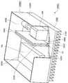
- FIG. 6 is a perspective view showing the internal configuration of the electronic apparatus 1000A.
- the electronic device 1000A is, for example, a microwave power module. In the following description, the electronic device 1000A will be described as a microwave power module.
- constituent elements equivalent to those shown in FIGS. 1 to 5 are given the same reference numerals as those shown in FIGS.
- the electronic apparatus 1000 in the first embodiment is compared with the electronic apparatus 1000A in the second embodiment.
- the electronic device 1000 was compatible with forced air cooling.
- the electronic device 1000A does not support forced air cooling. That is, the electronic component housing device 2000A of the electronic device 1000A is a sealed casing and does not take in or discharge air from the outside. For this reason, the electronic device 1000A is different from the electronic device 1000 in that the first fan unit 400 and the second fan unit 500 are not provided. Also, the electronic component housing device 2000A of the electronic device 1000A is different from the electronic component housing device 2000 of the electronic device 1000 in that the inflow port 700 and the discharge port 800 are not provided.
- the heat sink 300, the control module 600, the waveguide 900, the handle 2111, the opening window 2112, and the like are not provided in the electronic device 1000A, but these can be provided.
- the electronic device 1000 ⁇ / b> A includes a high voltage power supply module 100, a TWT 200, an electronic component housing device 2000 ⁇ / b> A, and a heat sink 3000.
- an electronic component housing device 2000A includes a housing 2100A, a first bottom plate 2300, a second bottom plate 2400, a first partition plate 2500, and a second partition plate 2600. Have.
- the housing 2100 ⁇ / b> A houses the high voltage power supply module 100 and the TWT 200.
- the material of the housing 2100A for example, the strength, weight, and heat dissipation of the housing 2100A, the influence of magnetism on the TWT 200, and the like are taken into consideration as with the housing 2100.
- a metal such as aluminum is used as the material of the housing 2100A.
- the housing 2100A is formed in a box shape.
- the housing 2100A is formed so that the inside is sealed. Thereby, the electronic apparatus 1000A can be installed outdoors.
- the upper cover is not shown. By attaching the upper cover by welding or screwing, the inside of the housing 2100A is sealed.
- the interior of the housing 2100 ⁇ / b> A is accommodated in the first electronic component housing by the first partition plate 2500 and the second partition plate 2600, as in the housing 2100 of the first embodiment. It is divided into a chamber 5000 and a second electronic component housing chamber 6000.
- the first electronic component storage chamber 5000 stores at least the high voltage power supply module 100.
- Second electronic component storage chamber 6000 stores at least TWT 200.
- the communication unit 7000 is provided between the first electronic component storage chamber 5000 and the second electronic component storage chamber 6000.
- the communication unit 7000 communicates between the first electronic component storage chamber 5000 and the second electronic component storage chamber 6000.
- first bottom plate 2300, the second bottom plate 2400, the first partition plate 2500, and the second partition plate 2600 are provided in the housing 2100A in the same manner as the electronic component housing device 2000 of the first embodiment. It has been.
- the heat sink 3000 is attached to the second bottom plate 2400 of the housing 2100A from the outside of the housing 2100A.
- the heat sink 3000 has a plurality of fins 3100.
- the plurality of fins 3100 are formed on the heat sink 3000 so as to extend in a direction perpendicular to the second bottom plate 2400 and away from the second bottom plate 2400.
- the heat sink 3000 corresponds to a heat dissipation unit.
- the configuration of the electronic device 1000A has been described above.
- the high voltage power supply module 100 supplies power to the TWT 200.
- the TWT 200 operates.
- the TWT 200, the high voltage power supply module 100, etc. generate heat.
- the electronic apparatus 1000A a cooling operation by heat conduction of the housing 2100A itself is adopted as the cooling operation of the electronic components in the housing 2100A.
- the electronic apparatus 1000A is different from the electronic apparatus 1000 in that the cooling operation by forced air cooling of the air in the housing 2100A is not adopted.
- the high voltage power supply module 100 is installed on the first bottom plate 2300. For this reason, the heat of the high voltage power supply module 100 is transferred to the first bottom plate 2300. That is, the heat energy of the high voltage power supply module 100 is applied to the first bottom plate 2300. The heat of the high voltage power supply module 100 is also transferred to the first partition plate 2500 by the first bottom plate 2300. In this way, the heat of the high voltage power supply module 100 is cooled by the heat received by the first bottom plate 2300 and the first partition plate 2500.
- the TWT 200 is installed on the second bottom plate 2400. For this reason, the heat of the TWT 200 is transferred to the second bottom plate 2400. That is, the thermal energy of the TWT 200 is applied to the second bottom plate 2400. The heat of the TWT 200 is also transferred to the second partition plate 2600 via the second bottom plate 2400. Thus, the heat of TWT 200 is cooled by the heat received by second bottom plate 2400 and second partition plate 2600. Furthermore, the heat sink 3000 is attached to the second bottom plate 2400 of the housing 2100A from the outside of the housing 2100A. Therefore, the heat sink 3000 receives the heat of the TWT 200 via the second bottom plate 2400 and radiates this heat to the outside air of the housing 2100A.
- the heat of the high voltage power supply module 100 is transferred to the first partition plate 2500 through the air in the first electronic component housing chamber 5000.
- the heat of the high voltage power supply module 100 is cooled by the heat received by the first partition plate 2500.
- the heat of TWT 200 is transferred to second partition plate 2600 through the air in second electronic component housing chamber 6000. Thereby, the heat of TWT 200 is cooled by the heat received by second partition plate 2600.
- the effect obtained by providing the first gap G1 between the first partition plate 2500 and the second partition plate 2600 is as described in the first embodiment. Further, the effect obtained by providing the second gap G2 between the first bottom plate 2300 and the second bottom plate 2400 is also as described in the first embodiment. Furthermore, the effect of communicating the first gap portion G1 and the second gap portion G2 is also as described in the first embodiment.
- the housing 2100A is formed so that the inside is sealed. Further, in the electronic apparatus 1000A, a cooling operation by heat conduction of the housing 2100A itself is adopted as a cooling operation of the electronic components in the housing 2100A. For this reason, the heat energy of the high voltage power supply module 100 and the TWT 200 is transported to the entire housing 2100A by the heat conduction of the housing 2100A itself. Therefore, the temperature inside the housing 2100A tends to rise uniformly.
- the heat sink 3000 is thermally connected to the second bottom plate 2400 to dissipate the heat of the TWT 200. Thereby, the heat of the TWT 200 is radiated to the outside of the housing 2100A via the heat sink 3000.
- the electronic component housing device 2000A and the electronic device 1000A according to the second embodiment of the present invention include the heat sink 3000 (heat radiating unit).
- the heat sink 3000 is thermally connected to the second bottom plate 2400 and radiates the heat of the TWT 200.
- the heat of the TWT 200 is radiated to the outside of the housing 2100A through the heat sink 300. Therefore, the heat of the TWT 200 that generates a larger amount of heat than the high voltage power supply module 100 can be prevented from being applied to the voltage power supply module 100. Therefore, it can suppress that the temperature of the high voltage power supply module 100 rises by the heat of the TWT 200.
- the heat sink 3000 As described above, by providing the heat sink 3000, the heat of the TWT 200, which generates a larger amount of heat than the high voltage power supply module 100, is more efficiently suppressed and the heat of the TWT 200 is more efficiently suppressed. Can be cooled.
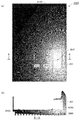
- FIG. 7 is a diagram showing a heat dissipation simulation result of the electronic device 1000A.
- FIG. 7A is a top view showing a heat radiation simulation result of the electronic apparatus 1000A.
- FIG. 7B is a cross-sectional view showing a heat dissipation simulation result of the electronic apparatus 1000A, and is a cross-sectional view taken along the line AA in FIG.
- FIG. 7A and FIG. 7B show the gradient of the temperature change.
- FIG. 7A and FIG. 7B show that the color in the region becomes brighter as the temperature in the region increases.
- the outer shape of the housing 2100A was set to 200 mm ⁇ 300 mm ⁇ 50 mm.
- the external dimensions of the heat sink 3000 were set to 300 mm ⁇ 200 mm ⁇ 10 mm.
- the material of the housing 2100A and the heat sink 3000 was set as an aluminum alloy.
- the shape of the TWT 200 is simplified for convenience. Further, in order to confirm the heat transfer path of the TWT 200, the high voltage power supply module 100 is omitted in FIGS. 7 (a) and 7 (b). 7A and 7B, only the collector 201 having a particularly large calorific value is shown in the TWT 200, and the configuration other than the collector 201 is omitted.
- the second gap G2 is provided between the first bottom plate 2300 and the second bottom plate 2400 over the entire region corresponding to the first electronic component storage chamber 5000.
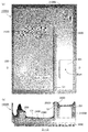
- FIG. 8 is a view showing a heat radiation simulation result of a comparative example of the electronic apparatus 1000A.
- FIG. 8A is a top view illustrating a heat dissipation simulation result of a comparative example of the electronic apparatus 1000A.
- FIG. 8B is a cross-sectional view showing a heat dissipation simulation result of a comparative example of the electronic apparatus 1000A, and is a cross-sectional view taken along the line BB of FIG. 8A.
- FIG. 8A and FIG. 8B show the gradient of the temperature change. In FIG. 8A and FIG. 8B, the color in the region is shown to become brighter as the temperature in the region becomes higher.
- the outer shape of the housing 9100 was set to 200 mm ⁇ 300 mm ⁇ 50 mm.
- the external dimensions of the heat sink 3000 were set to 300 mm ⁇ 200 mm ⁇ 10 mm.
- the material of the housing 9100 and the heat sink 3000 was set as an aluminum alloy.
- the housing 9100 is not provided with the first partition plate 2500 and the second partition plate 2600. Further, the first bottom plate 2300 and the second bottom plate 2400 are not provided, and only one bottom plate 9200 is provided.
- the size of the housing 9100 of the electronic device 8000 is substantially the same as the size of the housing 2100A of the electronic device 1000A. 8A and 8B, only the collector 201 having a particularly large calorific value is shown in the TWT 200, and the configuration other than the collector 201 is omitted. Further, in order to confirm the heat transfer path of the collector 201 of the TWT 200, the high voltage power supply module 100 is omitted in FIGS. 8 (a) and 8 (b).
- the point a1 is set at the center of the collector 201 of the TWT 200.
- the points b1 and c1 are provided on a cutting plane AA extending in a direction perpendicular to the first partition plate 2500 and the second partition plate 2600.
- the cutting plane AA is set on the point a1.
- the distance between the point b1 and the first partition plate 2500 is set to be smaller than the distance between the point c1 and the first partition plate 2500.
- the distance between the point b1 and the point a1 is set to be smaller than the distance between the point c1 and the point a1.
- the temperature rise at the point a1 of the collector 201 of the TWT 200 (temperature rise before and after the operation of the TWT 200 (for example, 15 minutes)) is assumed to be ⁇ Ta1 (deg).
- points a2, b2 and c2 are set at positions corresponding to points a1, b1 and c1 in FIG. 7A. That is, the point a2 is set at the center of the collector 201 of the TWT 200. The points b2 and c2 are provided on the cutting plane BB.
- the cutting plane BB corresponds to the cutting plane AA in FIG. Further, the cutting plane BB is set on the point a2. Furthermore, the distance between the point b2 and the point a2 is set to be smaller than the distance between the point c2 and the point a2.
- the temperature of the housing 9100 decreases as the temperature of the housing 9100 increases from the collector 201 of the TWT 200.
- the electronic device 8000 has a larger temperature change gradient near the collector 201 of the TWT 200 than the electronic device 1000A.
- the temperature rise at the point a2 of the collector 201 of the TWT 200 is set to ⁇ Ta2 (deg).
- the electronic device 8000 of the comparative example has a larger temperature rise than the electronic device 1000A. Therefore, in the electronic apparatus 1000A, the first partition plate 2500 and the second partition plate 2600 are provided, so that the heat of the collector 201 of the TWT 200 accommodates the first electronic component housing the high voltage power supply module 100. It can be seen that transmission to the chamber 5000 can be suppressed. It can also be seen that the thermal energy transport of the collector 201 of the TWT 200 has a certain directionality.
- the temperature rise at the point b1 (corresponding to the point b2) is smaller than that of the electronic device 8000. That is, in the electronic apparatus 1000A, the first partition plate 2500 and the second partition plate 2600 are provided, so that the temperature rise on the first electronic component storage chamber 5000 side even in the region close to the collector 201 of the TWT 200. Is suppressed compared to the electronic device 8000. Thereby, in the electronic device 8000, the low heat resistant electronic component mounted in the region away from the collector 201 of the TWT 200 is placed in the vicinity of the collector 201 of the TWT 200 on the first electronic component storage chamber 5000 side (for example, the point b1). Can be implemented. Therefore, the electronic device 1000A can improve the degree of freedom in mounting design as compared with the electronic device 8000.
- FIG. 9 is a diagram showing a heat dissipation simulation result of the electronic apparatus 1000A.
- FIG. 9A is a top view showing a heat radiation simulation result of the electronic apparatus 1000A.
- FIG. 9B is a cross-sectional view showing a heat radiation simulation result of the electronic apparatus 1000A, and is a cross-sectional view taken along the line CC in FIG. 9A.
- 9A and 9B show the gradient of the temperature change.
- FIG. 9A and FIG. 9B show that the color in the region becomes brighter as the temperature in the region increases.
- the outer shape of the housing 2100A was set to 200 mm ⁇ 300 mm ⁇ 50 mm.
- the external dimensions of the heat sink 3000 were set to 300 mm ⁇ 200 mm ⁇ 10 mm.
- the material of the housing 2100A and the heat sink 3000 was set as an aluminum alloy.
- the collector 201 having a particularly large calorific value is shown in the TWT 200, and the configuration other than the collector 201 is omitted.
- the high voltage power supply module 100 is omitted in FIGS. 9 (a) and 9 (b).
- 9A and 9B unlike FIGS. 7A and 7B, the heating element 250 is mounted in the first electronic component housing chamber 5000.
- the second gap G2 is provided between the first bottom plate 2300 and the second bottom plate 2400 over the entire region corresponding to the first electronic component storage chamber 5000.
- the heat generation amount of the heating element 250 is, for example, about the same as or lower than the heat generation amount of the TWT 200.
- FIG. 10 is a diagram illustrating a heat dissipation simulation result of a modified example of the electronic apparatus 1000A.
- FIG. 10A is a top view showing a heat radiation simulation result of a modification of the electronic apparatus 1000A.
- FIG. 10B is a cross-sectional view showing a heat dissipation simulation result of a modified example of the electronic apparatus 1000A, and is a cross-sectional view taken along the line DD in FIG. 10A and 10B show the gradient of the temperature change.
- FIG. 10A and FIG. 10B show that the color in the region becomes brighter as the temperature in the region increases.
- the outer shape of the housing 2100B was set to 200 mm ⁇ 300 mm ⁇ 50 mm.
- the external dimensions of the heat sink 3000 were set to 300 mm ⁇ 200 mm ⁇ 10 mm.
- the material of the housing 2100B and the heat sink 3000 was set as an aluminum alloy.
- the housing 2100B of the electronic component housing device 2000B includes a first partition plate 2500, a second partition plate 2600, The first bottom plate 2300 and the second bottom plate 2400 are provided.
- the mounting region of the heating element 250 is different from the electronic device 1000 ⁇ / b> A in that the double structure of the first bottom plate 2300 and the second bottom plate 2400 is not formed.
- the size of the housing 2100B of the electronic device 1000B is substantially the same as the size of the electronic device 1000A.
- FIGS. 10A and 10B only the collector 201 having a particularly large calorific value is shown in the TWT 200, and the configuration other than the collector 201 is omitted. Further, in order to confirm the heat transfer path of the TWT 200, the high voltage power supply module 100 is omitted in FIGS. 10 (a) and 10 (b). Also, in FIGS. 10A and 10B, unlike FIGS. 7A and 7B, the heating element 250 is mounted in the first electronic component housing chamber 5000. FIG.
- the heat generation amount of the heating element 250 is, for example, about the same as or lower than the heat generation amount of the TWT 200.
- the point a3 is set at the center of the collector 201 of the TWT 200.
- the points b3 and c3 are provided on a cutting plane CC extending in a direction perpendicular to the first partition plate 2500 and the second partition plate 2600.
- the cutting plane CC is set on the point a3.
- the distance between the point b3 and the first partition plate 2500 is set to be smaller than the distance between the point c3 and the first partition plate 2500.
- the positions of the points a3, b3, and c3 correspond to the positions of the points a1, b1, and c1 in FIG.
- the temperature rise at the point a3 of the collector 201 of the TWT 200 (temperature rise before and after the operation of the TWT 200 (for example, 15 minutes)) is assumed to be ⁇ Ta3 (deg).
- points a4, b4 and c4 are set at positions corresponding to points a3, b3 and c3 in FIG. 9A. That is, the point a4 is set at the center of the collector 201 of the TWT 200. The points b4 and c4 are provided on the cut surface DD corresponding to the cut surface CC in FIG. The cutting plane DD is set on the point a4. Further, the distance between the point b4 and the point a4 is set to be smaller than the distance between the point c4 and the point a4.
- the temperature rise at the point a4 of the collector 201 of the TWT 200 (temperature rise before and after the operation of the TWT 200 (for example, 15 minutes)) is assumed to be ⁇ Ta4 (deg).
- the double structure of the first bottom plate 2300 and the second bottom plate 2400 is formed. Is not transmitted directly to the heat sink 3000 side. For this reason, the temperature at the point c3 is greatly increased as compared with the point c4 in FIG.
- the heating element 250 in the mounting region of the heating element 250, by not forming the double structure of the first bottom plate 2300 and the second bottom plate 2400, the heating element The heat of 250 can be directly transferred to the heat sink 3000 side. As a result, the temperature around the heating element 250 can be lowered as compared with the electronic device 1000A.
- the double structure of the first bottom plate 2300 and the second bottom plate 2400 in the mounting region of the electronic component in accordance with the heat generation amount of the electronic component mounted in the first electronic component storage chamber 5000 By not forming, the temperature rise around the electronic component can be suppressed. As a result, the degree of freedom of electronic component mounting design can be improved.
- FIG. 11 is a perspective view showing an internal configuration of the electronic apparatus 1000C.
- the electronic device 1000C is, for example, a microwave power module. In the following description, the electronic device 1000C will be described as a microwave power module.
- the same reference numerals as those shown in FIGS. 1 to 10 are attached to the same constituent elements as those shown in FIGS.
- the electronic apparatus 1000A in the second embodiment is compared with the electronic apparatus 1000C in the third embodiment.
- the electronic device 1000A and the electronic device 1000C are common in that they do not support forced air cooling.
- the electronic component housing device 2000C of the electronic device 1000C is a sealed casing and does not take in or discharge air from the outside.
- the electronic device 1000C is different from the electronic device 1000A in that the first bottom plate 2300 and the second bottom plate 2400 are not arranged to face each other. Accordingly, the gap G2 is not provided between the first bottom plate 2300 and the second bottom plate 2400.
- the electronic device 1000 ⁇ / b> C includes a high voltage power supply module 100, a TWT 200, an electronic component housing device 2000 ⁇ / b> C, and a heat sink 3000.
- the heat sink 3000 is not essential to the present embodiment. That is, the electronic device 1000C according to the third embodiment can be configured without providing the heat sink 3000.
- the electronic component housing device 2000C includes a housing 2100C, a first bottom plate 2300, a second bottom plate 2400, a first partition plate 2500, and a second partition plate 2600. Have.
- the housing 2100 ⁇ / b> C houses the high voltage power supply module 100 and the TWT 200.
- the material of the housing 2100C for example, the strength, weight and heat dissipation of the housing 2100C, the influence of magnetism on the TWT 200, and the like are taken into consideration, as with the housing 2100.
- a metal such as aluminum is used as the material of the housing 2100C.
- the housing 2100C is formed in a box shape.
- the housing 2100C is formed so that the inside is sealed. Thereby, the electronic device 1000C can be installed outdoors.
- the upper cover is not shown. By attaching the upper cover by welding or screwing, the inside of the housing 2100C is sealed.
- the inside of the housing 2100C is similar to the housing 2100A by the first partition plate 2500 and the second partition plate 2600, and the first electronic component housing chamber 5000 and the second partition plate 2600. It is divided into an electronic component storage chamber 6000.
- the first electronic component storage chamber 5000 stores at least the high voltage power supply module 100.
- Second electronic component storage chamber 6000 stores at least TWT 200.
- the communication unit 7000 is provided between the first electronic component storage chamber 5000 and the second electronic component storage chamber 6000.
- the communication unit 7000 communicates between the first electronic component storage chamber 5000 and the second electronic component storage chamber 6000.
- the first bottom plate 2300, the second bottom plate 2400, the first partition plate 2500, and the second partition plate 2600 are provided in the housing 2100C.
- the first bottom plate 2300 and the second bottom plate 2400 are not arranged to face each other.
- no gap G2 is provided between the first bottom plate 2300 and the second bottom plate 2400.
- the first partition plate 2500 and the second partition plate 2600 are arranged to face each other.
- a gap G ⁇ b> 1 is provided between the first partition plate 2500 and the second partition plate 2600.
- the heat sink 3000 is attached to the first bottom plate 2300 and the second bottom plate 2400 of the housing 2100C from the outside of the housing 2100C.
- the high voltage power supply module 100 supplies power to the TWT 200.
- the TWT 200 operates.
- the TWT 200, the high voltage power supply module 100, etc. generate heat.
- a cooling operation by heat conduction of the housing 2100C itself is adopted as the cooling operation of the electronic components in the housing 2100C.
- the high voltage power supply module 100 is installed on the first bottom plate 2300. For this reason, the heat of the high voltage power supply module 100 is transferred to the first bottom plate 2300. That is, the heat energy of the high voltage power supply module 100 is applied to the first bottom plate 2300. The heat of the high voltage power supply module 100 is also transferred to the first partition plate 2500 by the first bottom plate 2300. Thereby, the heat of the high voltage power supply module 100 is cooled by the heat received by the first bottom plate 2300 and the first partition plate 2500.
- the TWT 200 is installed on the second bottom plate 2400. For this reason, the heat of the TWT 200 is transferred to the second bottom plate 2400. That is, the thermal energy of the TWT 200 is applied to the second bottom plate 2400. The heat of the TWT 200 is also transferred to the second partition plate 2600 via the second bottom plate 2400. Thereby, the heat of TWT 200 is cooled by the heat received by second bottom plate 2400 and second partition plate 2600.
- the heat sink 3000 is attached to the first bottom plate 2300 and the second bottom plate 2400 of the housing 2100C from the outside of the housing 2100C. Accordingly, the heat sink 3000 receives the heat of the TWT 200 via the second bottom plate 2400 and radiates this heat to the outside air of the housing 2100C.
- the heat of the high voltage power supply module 100 is transferred to the first partition plate 2500 through the air in the first electronic component housing chamber 5000. Thereby, the heat of the high voltage power supply module 100 is cooled by the heat received by the first partition plate 2500.
- the heat of TWT 200 is transferred to second partition plate 2600 through the air in second electronic component housing chamber 6000. Thereby, the heat of TWT 200 is cooled by the heat received by second partition plate 2600.
- a first gap G1 is provided between the first partition plate 2500 and the second partition plate 2600. That is, the first partition plate 2500 and the second partition plate 2600 are separated from each other. For this reason, direct heat conduction between the first partition plate 2500 and the second partition plate 2600 does not occur. That is, direct transport of thermal energy due to heat conduction inside the first partition plate 2500 and the second partition plate 2600 does not occur between the first partition plate 2500 and the second partition plate 2600. That is, by providing the first gap G1 between the first partition plate 2500 and the second partition plate 2600, the space between the first electronic component storage chamber 5000 and the second electronic component storage chamber 6000 is reduced. Heat transfer can be suppressed.
- the heat of the TWT 200 that generates a larger amount of heat than the high voltage power supply module 100 is suppressed from being applied to the high voltage power supply module 100 via the first partition plate 2500 and the second partition plate 2600. Thereby, it can suppress that the temperature of the high voltage power supply module 100 rises with the heat of TWT200. Therefore, it can suppress that the performance of the high voltage power supply module 100 deteriorates with the heat
- the heat of the TWT 200 which generates a larger amount of heat than the high voltage power supply module 100, is suppressed from being applied to the high voltage power supply module 100, and the TWT 200 and the high voltage power supply module 100 Heat can be efficiently cooled.
- the electronic component housing device 2000C includes the housing 2100C, the first electronic component housing chamber 5000, the second electronic component housing chamber 6000, and the first partition.
- a plate 2500 and a second partition plate 2600 are provided.
- the housing 2100C accommodates the high voltage power supply module 100 (first electronic component) and the TWT 200 (second electronic component).
- the TWT 200 generates a larger amount of heat than the high voltage power supply module 100.
- the first electronic component housing chamber 5000 houses the high voltage power supply module 100.
- Second electronic component storage chamber 6000 stores TWT 200.
- the first partition plate 2500 is disposed between the first electronic component storage chamber 5000 and the second electronic component storage chamber 6000 and on the first electronic component storage chamber 5000 side.
- the second partition plate 2600 is disposed between the first electronic component storage chamber 5000 and the second electronic component storage chamber 6000 and on the second electronic component storage chamber 6000 side.
- the first partition plate 2500 and the second partition plate 2600 are provided so as to face each other at least partially.
- a first gap G ⁇ b> 1 is provided between the first partition plate 2500 and the second partition plate 2600.
- the housing 2100C is used for the first electronic component housing chamber 5000 and the second electronic component housing chamber 6000 using the first partition plate 2500 and the second partition plate 2600. It is divided into.
- the first electronic component housing chamber 5000 houses the high voltage power supply module 100.
- Second electronic component storage chamber 6000 stores TWT 200. That is, in the electronic component housing device 2000C, the first partition plate 2500 and the second partition plate 2600 are provided, and the high voltage power supply module 100 and the TWT 200 are housed in separate housing chambers. Thereby, it can suppress that the heat of TWT200 applies to the high voltage power supply module 100 via the air in the housing
- a first gap G1 is provided between the first partition plate 2500 and the second partition plate 2600. That is, the first partition plate 2500 and the second partition plate 2600 are separated from each other. For this reason, direct heat conduction between the first partition plate 2500 and the second partition plate 2600 does not occur. That is, by providing the first gap G1 between the first partition plate 2500 and the second partition plate 2600, the space between the first electronic component storage chamber 5000 and the second electronic component storage chamber 6000 is reduced. Heat transfer can be suppressed. Therefore, it is possible to suppress the heat of the TWT 200 having a larger calorific value than that of the high voltage power supply module 100 from being applied to the high voltage power supply module 100 via the first partition plate 2500 and the second partition plate 2600. Thereby, it can suppress that the temperature of the high voltage power supply module 100 rises with the heat of TWT200.
- the heat of the TWT 200 which generates a larger amount of heat than the high voltage power supply module 100, is prevented from being applied to the high voltage power supply module 100, and the heat of the TWT 200 is efficiently obtained. Can be cooled.
- FIG. 12 is a perspective view showing an internal configuration of the electronic apparatus 1000D.
- the electronic device 1000D is, for example, a microwave power module.
- electronic device 1000D will be described as a microwave power module.
- FIG. 12 the same components as those shown in FIGS. 1 to 11 are denoted by the same reference numerals as those shown in FIGS.
- the electronic device 1000A in the second embodiment is compared with the electronic device 1000D in the fourth embodiment.
- Electronic device 1000D and electronic device 1000A are common in that they do not support forced air cooling. That is, the electronic component housing device 2000D of the electronic device 1000D is a sealed housing and does not take in or discharge air from the outside.
- the electronic device 1000D is different from the electronic device 1000A in that the first partition plate 2500 and the second partition plate 2600 are not provided.
- the electronic device 1000D includes a high-voltage power supply module 100, a TWT 200, an electronic component housing device 2000D, and a heat sink 3000.
- the heat sink 3000 is not essential to the embodiment of the present invention. That is, the electronic device 1000D according to the fourth embodiment can be configured without providing the heat sink 3000.
- the electronic component housing device 2000D includes a housing 2100D, a first bottom plate 2300, and a second bottom plate 2400.
- the housing 2100D houses the high-voltage power supply module 100 and the TWT 200.
- the material of the housing 2100D for example, the strength, weight, and heat dissipation of the housing 2100D, the influence of magnetism on the TWT 200, and the like are taken into consideration as in the housing 2100.
- a metal such as aluminum is used as the material of the housing 2100D.
- the housing 2100D is formed in a box shape.
- the housing 2100D is formed so that the inside is sealed.
- electronic device 1000D can be installed outdoors.
- the upper cover is not shown. By attaching the upper cover by welding or screwing, the inside of the housing 2100D is sealed.
- the first bottom plate 2300 and the second bottom plate 2400 are provided in the housing 2100D.
- the high voltage power supply module 100 is provided on the first bottom plate 2300.
- the TWT 200 is provided on the second bottom plate 2400.
- the heat sink 3000 is attached to the second bottom plate 2400 of the housing 2100D from the outside of the housing 2100D.
- the configuration of the electronic device 1000D has been described above.
- the high voltage power supply module 100 supplies power to the TWT 200.
- the TWT 200 operates.
- the TWT 200, the high voltage power supply module 100, etc. generate heat.
- a cooling operation by heat conduction of the housing 2100D itself is adopted as a cooling operation of the electronic components in the housing 2100D.
- the high voltage power supply module 100 is installed on the first bottom plate 2300. For this reason, the heat of the high voltage power supply module 100 is transferred to the first bottom plate 2300. That is, the heat energy of the high voltage power supply module 100 is applied to the first bottom plate 2300. Thereby, the heat of the high voltage power supply module 100 is cooled by the heat received by the first bottom plate 2300.
- the TWT 200 is installed on the second bottom plate 2400. For this reason, the heat of the TWT 200 is transferred to the second bottom plate 2400. That is, the thermal energy of the TWT 200 is applied to the second bottom plate 2400. As a result, the heat of the TWT 200 is cooled by the heat received by the second bottom plate 2400.
- the heat sink 3000 is attached to the second bottom plate 2400 of the housing 2100D from the outside of the housing 2100D. Therefore, the heat sink 3000 receives the heat of the TWT 200 via the second bottom plate 2400 and dissipates this heat to the outside air of the housing 2100D.
- a second gap G ⁇ b> 2 is provided between the first bottom plate 2300 and the second bottom plate 2400. That is, the first bottom plate 2300 and the second bottom plate 2400 are separated from each other in a partial region. Therefore, at least in a part of the region where the first bottom plate 2300 and the second bottom plate 2400 are separated from each other, direct heat conduction does not occur between the first bottom plate 2300 and the second bottom plate 2400. . That is, at least in a part of the region where the first bottom plate 2300 and the second bottom plate 2400 are separated from each other, heat energy is transferred by heat conduction inside the first bottom plate 2300 and the second bottom plate 2400. Absent.
- the heat of the TWT 200 that generates a larger amount of heat than the high-voltage power supply module 100 is generated.
- the high voltage power supply module 100 is not applied via the second bottom plate 2400. Therefore, compared with the case where there is no region where the first bottom plate 2300 and the second bottom plate 2400 are separated from each other, the heat of the TWT 200 that generates a larger amount of heat than the high voltage power supply module 100 is generated in the high voltage power supply module 100. It can suppress adding. Thereby, it can suppress that the temperature of the high voltage power supply module 100 rises with the heat of TWT200. Therefore, it can suppress that the performance of the high voltage power supply module 100 deteriorates with the heat
- the heat of the TWT 200 is not transmitted to the high voltage power supply module 100 via the first bottom plate 2300 and the second bottom plate 2400. For this reason, the heat of the TWT 200 is easily transferred to the heat sink 3000 via the second bottom plate 2400.
- the high voltage power supply module 100 and the high voltage power supply module 100 can be prevented from applying heat to the high voltage power supply module 100 with the heat generation amount larger than that of the high voltage power supply module 100.
- the heat of the TWT 200 can be efficiently cooled.
- the electronic component housing device 2000D includes the housing 2100D, the first bottom plate 2300, and the second bottom plate 2400.
- the housing 2100D houses the high-voltage power supply module 100 (first electronic component) and the TWT 200 (second electronic component) that generates a larger amount of heat than the high-voltage power supply module 100.
- the first bottom plate 2300 is a part of the housing 2100. On the first bottom plate 2300, the high-voltage power supply module 100 (first electronic component) is installed.
- the first bottom plate 2300 is thermally connected to the high voltage power supply module 100.
- the second bottom plate 2400 is a part of the housing 2100.
- the second bottom plate 2400 is provided with TWT 200 (second electronic component). Second bottom plate 2400 is thermally connected to TWT 200.
- the first bottom plate 2300 and the second bottom plate 2400 are provided so as to face each other at least partially.
- a second gap G2 is provided between the first bottom plate 2300 and the second bottom plate 2400.
- the high voltage power supply module 100 is installed on the first bottom plate 2300.
- the first bottom plate 2300 is thermally connected to the high voltage power supply module 100.
- the TWT 200 is installed on the second bottom plate 2400.
- Second bottom plate 2400 is thermally connected to TWT 200. Therefore, the heat of the high voltage power supply module 100 is transferred to the first bottom plate 2300.
- the heat of the TWT 200 is transferred to the second bottom plate 2400.
- a second gap G2 is provided between the first bottom plate 2300 and the second bottom plate 2400. That is, the first bottom plate 2300 and the second bottom plate 2400 are separated from each other.
- the high voltage power supply module 100 and the high voltage power supply module 100 can be prevented from applying heat to the high voltage power supply module 100 with the heat generation amount larger than that of the high voltage power supply module 100.
- the heat of the TWT 200 can be cooled.
- the electronic device 1000D includes a high-voltage power supply module 100 (first electronic component), a TWT 200 (second electronic component), a housing 2100D, and a first bottom plate. 2300 and a second bottom plate 2400.
- the TWT 200 generates a larger amount of heat than the high voltage power supply module 100.
- the housing 2100D houses the high voltage power supply module 100 and the TWT 200.
- the first bottom plate 2300 is a part of the housing 2100D.
- the high voltage power supply module 100 is installed on the first bottom plate 2300.
- the first bottom plate 2300 is thermally connected to the high voltage power supply module 100.
- the second bottom plate 2400 is a part of the housing 2100.
- the TWT 200 is installed on the second bottom plate 2400. Second bottom plate 2400 is thermally connected to TWT 200.
- the first bottom plate 2300 and the second bottom plate 2400 are provided so as to face each other at least partially.
- a second gap G2 is provided between the first bottom plate 2300 and the second bottom plate 2400.
- a heat insulating member (not shown) that suppresses heat transfer in the first gap G1 may be provided in the first gap G1. Thereby, it can suppress more effectively that the heat of TWT200 moves from the 2nd partition plate 2600 to the 1st partition plate 2500 via the air in the 1st space G1. Further, a heat insulating member that suppresses heat transfer in the second gap G2 may be provided in the second gap G2. Thereby, it can suppress more effectively that the heat of TWT200 moves from the 2nd bottom plate 2400 to the 1st bottom plate 2300 via the air in the 2nd space G2.
- the high voltage power supply module 100 can be mounted on the first bottom plate 2300 via a pedestal (not shown). Thereby, it can further suppress that the heat of TWT200 is transmitted to the high voltage power supply module 100.
- FIG. it is effective when the first bottom plate 2300 and the second bottom plate 2400 are arranged so as not to face each other as in the electronic device 1000C in the third embodiment.
- first partition plate 2500 and the second partition plate 2600 an example in which there is no physical connection between the first partition plate 2500 and the second partition plate 2600 is shown.
- first gap G1 is provided between the first partition plate 2500 and the second partition plate 2600, the space between the first partition plate 2500 and the second partition plate 2600 is physically separated. It may be connected.
- the upper cover 2140 is attached to the body portion 2130, the leading end portions of the first partition plate 2500 and the second partition plate 2600 may be connected to the inner surface of the upper cover 2140.
- a part or all of each of the above-described embodiments may be described as follows, but is not limited to the following.
- Appendix 1 A first electronic component, and a housing that houses a second electronic component that generates a larger amount of heat than the first electronic component;
- a first electronic component housing chamber for housing the first electronic component;
- a second electronic component housing chamber for housing the second electronic component;
- a first partition plate disposed between the first electronic component storage chamber and the second electronic component storage chamber and disposed on the first electronic component storage chamber side;
- a second partition plate disposed between the first electronic component storage chamber and the second electronic component storage chamber and disposed on the second electronic component storage chamber side;
- the first partition plate and the second partition plate are provided to face each other at least in part,
- An electronic component housing device in which a first gap is provided between the first partition plate and the second partition plate.
- the first bottom plate and the second bottom plate are provided so as to face each other at least in part,
- a second gap is provided between the first bottom plate and the second bottom plate,
- the first partition plate is connected to the first bottom plate, the second partition plate is connected to the second bottom plate,
- the first bottom plate and the second bottom plate are provided so as to face each other at least in part,
- a second gap is provided between the first bottom plate and the second bottom plate,
- the first partition plate is connected to the first bottom plate, the second partition plate is connected to the second bottom plate,
- the first bottom plate and the second bottom plate are provided so as to face each other at least in part,
- [Appendix 10] The electronic component housing device according to appendix 8 or 9, further comprising a heat radiating portion thermally connected to the second bottom plate and radiating heat of the second electronic component.
- Appendix 11 A communication portion that communicates between the first electronic component storage chamber and the second electronic component storage chamber; The electronic component housing device according to appendix 9 or 10, wherein a flow path of air flowing from the first electronic component housing chamber to the second electronic component housing chamber is formed via the communication portion.
- a housing that houses a first component and a second component that generates heat; A first component storage chamber for storing the first component; A second component storage chamber for storing the second component; A first partition plate disposed between the first component storage chamber and the second component storage chamber and disposed on the first component storage chamber side; A second partition plate disposed between the first electronic storage chamber and the second component storage chamber and disposed on the second electronic storage chamber side; A component housing device in which a first gap is provided between the first partition plate and the second partition plate.
- the first bottom plate and the second bottom plate are provided so as to face each other at least in part,
- a second gap is provided between the first bottom plate and the second bottom plate,
- the first partition plate is connected to the first bottom plate
- the second partition plate is connected to the second bottom plate
- the component housing device according to attachment 15 wherein the first gap portion and the second gap portion communicate with each other.
- the component housing device according to supplementary note 16 further comprising a heat radiating portion, thermally connected to the second bottom plate.
- [Appendix 18] A communication portion communicating between the first component storage chamber and the second component storage chamber; The component storage device according to any one of supplementary notes 15 to 17, wherein a flow path of air flowing from the first component storage chamber to the second component storage chamber is formed via the communication portion.
- [Appendix 19] The component storage device according to any one of supplementary notes 15 to 18, wherein a heat insulating member is provided in the first gap portion or the second gap portion.
- Appendix 20 The component storage device according to any one of appendices 15 to 19, A first part; An apparatus comprising the second component.
- a housing that houses a first component and a second component that generates heat; A first bottom plate that is a part of the housing, wherein the first component is installed and thermally connected to the first component; A second bottom plate that is a part of the housing, wherein the second component is installed and thermally connected to the second component; A component housing device in which a second gap is provided between the first bottom plate and the second bottom plate.
- [Appendix 22] A first electronic component housing chamber for housing the first component; A second electronic component housing chamber for housing the second component; A first partition plate disposed between the first component storage chamber and the second component storage chamber and disposed on the first component storage chamber side; A second partition plate disposed between the first component storage chamber and the second component storage chamber and disposed on the second component storage chamber side; A first gap is provided between the first partition plate and the second partition plate, The first partition plate is connected to the first bottom plate, the second partition plate is connected to the second bottom plate, The component housing device according to attachment 21, wherein the first gap portion and the second gap portion communicate with each other. [Appendix 23] 23. The component housing device according to appendix 21 or 22, further comprising a heat radiating portion that is thermally connected to the second bottom plate.
- [Appendix 24] A communication portion communicating between the first component storage chamber and the second component storage chamber; 24.
- [Appendix 25] The electronic component storage device according to any one of appendices 21 to 24, wherein a heat insulating member is provided in the first gap portion or the second gap portion.
- [Appendix 26] The parts storage device according to any one of appendices 21 to 25; The first part; An apparatus comprising the second component.
Landscapes
- Engineering & Computer Science (AREA)
- Microelectronics & Electronic Packaging (AREA)
- Physics & Mathematics (AREA)
- Thermal Sciences (AREA)
- Cooling Or The Like Of Electrical Apparatus (AREA)
- Cooling Or The Like Of Semiconductors Or Solid State Devices (AREA)
Abstract
Description
本発明の第1の実施の形態における電子装置1000の構成について説明する。図1は、電子装置1000の内部構成を示す斜視図である。図2は、電子装置1000の外観を前面側から視た斜視図である。図3は、電子装置1000の外観を背面側から視た斜視図である。図4は、電子装置1000の内部構成を示す上面図である。図5は、電子部品収容機器2000の内部構成を示す斜視図である。
本発明の第2の実施の形態における電子装置1000Aの構成について説明する。図6は、電子装置1000Aの内部構成を示す斜視図である。電子装置1000Aは、たとえば、マイクロ波電力モジュールである。以下の説明では、電子装置1000Aをマイクロ波電力モジュールとして説明する。なお、図6では、図1~図5で示した各構成要素と同等の構成要素には、図1~図5に示した符号と同等の符号を付している。
本発明の第3の実施の形態における電子装置1000Cの構成について説明する。図11は、電子装置1000Cの内部構成を示す斜視図である。電子装置1000Cは、たとえば、マイクロ波電力モジュールである。以下の説明では、電子装置1000Cをマイクロ波電力モジュールとして説明する。なお、図11では、図1~図10で示した各構成要素と同等の構成要素には、図1~図10に示した符号と同等の符号を付している。
本発明の第4の実施の形態における電子装置1000Dの構成について説明する。
図12は、電子装置1000Dの内部構成を示す斜視図である。電子装置1000Dは、たとえば、マイクロ波電力モジュールである。以下の説明では、電子装置1000Dをマイクロ波電力モジュールとして説明する。なお、図12では、図1~図11で示した各構成要素と同等の構成要素には、図1~図11に示した符号と同等の符号を付している。
[付記1]
第1の電子部品と、前記第1の電子部品よりも発熱量が大きい第2の電子部品を収容する筐体と、
前記第1の電子部品を収容する第1の電子部品収容室と、
前記第2の電子部品を収容する第2の電子部品収容室と、
前記第1の電子部品収容室および前記第2の電子部品収容室の間であって、前記第1の電子部品収容室側に配置された第1の仕切板と、
前記第1の電子部品収容室および前記第2の電子部品収容室の間であって、前記第2の電子器部品収容室側に配置された第2の仕切板と、
前記第1の仕切板および第2の仕切板は、少なくとも一部で互いに向かい合うように設けられ、
前記第1の仕切板および第2の仕切板の間には、第1の空隙部が設けられている電子部品収容機器。
[付記2]
前記筐体の一部であって、前記第1の電子部品が設置され、前記第1の電子部品に熱的に接続する第1の底板と、
前記筐体の一部であって、前記第2の電子部品が設置され、前記第2の電子部品に熱的に接続する第2の底板と、
前記第1の底板および第2の底板は、少なくとも一部で互いに向かい合うように設けられ、
前記第1の底板および第2の底板の間には第2の空隙部が設けられ、
前記第1の仕切板は前記第1の底板に接続され、前記第2の仕切板は前記第2の底板に接続され、
前記第1の空隙部および前記第2の空隙部は連通する付記1に記載の電子部品収容機器。
[付記3]
前記第2の底板に熱的に接続され、前記第2の電子部品の熱を放熱する放熱部をさらに備えた付記2に記載の電子部品収容機器。
[付記4]
前記第1の電子部品収容室および前記第2の電子部品収容室の間を連通する連通部とを備え、
前記連通部を介して、前記第1の電子部品収容室から前記第2の電子部品収容室へ流れる空気の流路が形成された付記1~3のいずれか1項に記載の電子部品収容機器。
[付記5]
前記第1の空隙部または前記第2の空隙部内の熱の移動を抑制する断熱部材が、前記第1の空隙部または前記第2の空隙部に設けられた付記1~4のいずれか1項に記載の電子部品収納機器。
[付記6]
第1の電子部品と、
前記第1の電子部品よりも発熱量が大きい第2の電子部品と、
第1の電子部品と前記第2の電子部品を収容する筐体と、
前記第1の電子部品を収容する第1の電子部品収容室と、
前記第2の電子部品を収容する第2の電子部品収容室と、
前記第1の電子部品収容室および前記第2の電子部品収容室の間であって、前記第1の電子器部品収容室側に配置された第1の仕切板と、
前記第1の電子部品収容室および前記第2の電子部品収容室の間であって、前記第2の電子器部品収容室側に配置された第2の仕切板と、
前記第1の仕切板および第2の仕切板は、少なくとも一部で互いに向かい合うように設けられ、
前記第1の仕切板および第2の仕切板の間には、第1の空隙部が設けられている電子装置。
[付記7]
前記筐体の一部であって、前記第1の電子部品が設置され、前記第1の電子部品に熱的に接続する第1の底板と、
前記筐体の一部であって、前記第2の電子部品が設置され、前記第2の電子部品に熱的に接続する第2の底板と、
前記第1の底板および第2の底板は、少なくとも一部で互いに向かい合うように設けられ、
前記第1の底板および第2の底板の間には第2の空隙部が設けられ、
前記第1の仕切板は前記第1の底板に接続され、前記第2の仕切板は前記第2の底板に接続され、
前記第1の空隙部および前記第2の空隙部は連通する付記6に記載の電子装置。
[付記8]
第1の電子部品と、前記第1の電子部品よりも発熱量が大きい第2の電子部品を収容する筐体と、
前記筐体の一部であって、前記第1の電子部品が設置され、前記第1の電子部品に熱的に接続する第1の底板と、
前記筐体の一部であって、前記第2の電子部品が設置され、前記第2の電子部品に熱的に接続する第2の底板と、
前記第1の底板および第2の底板は、少なくとも一部で互いに向かい合うように設けられ、
前記第1の底板および第2の底板の間には第2の空隙部が設けられた電子部品収容機器。
[付記9]
前記第1の電子部品を収容する第1の電子部品収容室と、
前記第2の電子部品を収容する第2の電子部品収容室と、
前記第1の電子部品収容室および前記第2の電子部品収容室の間であって、前記第1の電子器部品収容室側に配置された第1の仕切板と、
前記第1の電子部品収容室および前記第2の電子部品収容室の間であって、前記第2の電子器部品収容室側に配置された第2の仕切板と、
前記第1の仕切板および第2の仕切板は、少なくとも一部で互いに向かい合うように設けられ、
前記第1の仕切板および第2の仕切板の間には、第1の空隙部が設けられ、
前記第1の仕切板は前記第1の底板に接続され、前記第2の仕切板は前記第2の底板に接続され、
前記第1の空隙部および前記第2の空隙部は連通する付記8に記載の電子部品収容機器。
[付記10]
前記第2の底板に熱的に接続され、前記第2の電子部品の熱を放熱する放熱部をさらに備えた付記8または9に記載の電子部品収容機器。
[付記11]
前記第1の電子部品収容室および前記第2の電子部品収容室の間を連通する連通部とを備え、
前記連通部を介して、前記第1の電子部品収容室から前記第2の電子部品収容室へ流れる空気の流路が形成された付記9または10に記載の電子部品収容機器。
[付記12]
前記第1の空隙部または前記第2の空隙部内の熱の移動を抑制する断熱部材が、前記第1の空隙部または前記第2の空隙部に設けられた付記8~11のいずれか1項に記載の電子部品収納機器。
[付記13]
第1の電子部品と、
前記第1の電子部品よりも発熱量が大きい第2の電子部品と、
第1の電子部品と、前記第2の電子部品を収容する筐体と、
前記筐体の一部であって、前記第1の電子部品が設置され、前記第1の電子部品に熱的に接続する第1の底板と、
前記筐体の一部であって、前記第2の電子部品が設置され、前記第2の電子部品に熱的に接続する第2の底板と、
前記第1の底板および第2の底板は、少なくとも一部で互いに向かい合うように設けられ、
前記第1の底板および第2の底板の間には第2の空隙部が設けられた電子装置。
[付記14]
前記第1の電子部品を収容する第1の電子部品収容室と、
前記第2の電子部品を収容する第2の電子部品収容室と、
前記第1の電子部品収容室および前記第2の電子部品収容室の間であって、前記第1の電子器部品収容室側に配置された第1の仕切板と、
前記第1の電子部品収容室および前記第2の電子部品収容室の間であって、前記第2の電子器部品収容室側に配置された第2の仕切板と、
前記第1の仕切板および第2の仕切板は、少なくとも一部で互いに向かい合うように設けられ、
前記第1の仕切板および第2の仕切板の間には、第1の空隙部が設けられ、
前記第1の仕切板は前記第1の底板に接続され、前記第2の仕切板は前記第2の底板に接続され、
前記第1の空隙部および前記第2の空隙部は連通する付記13に記載の電子部品。
[付記15]
第1の部品と、発熱する第2の部品を収容する筐体と、
前記第1の部品を収容する第1の部品収容室と、
前記第2の部品を収容する第2の部品収容室と、
前記第1の部品収容室および前記第2の部品収容室の間であって、前記第1の部品収容室側に配置された第1の仕切板と、
前記第1の電子収容室および前記第2の部品収容室の間であって、前記第2の電子収容室側に配置された第2の仕切板とを備え、
前記第1の仕切板および第2の仕切板の間には、第1の空隙部が設けられている部品収容機器。
[付記16]
前記筐体の一部であって、前記第1の部品が設置され、前記第1の部品に熱的に接続する第1の底板と、
前記筐体の一部であって、前記第2の部品が設置され、前記第2の部品に熱的に接続する第2の底板とを備え、
前記第1の底板および第2の底板は、少なくとも一部で互いに向かい合うように設けられ、
前記第1の底板および第2の底板の間には第2の空隙部が設けられ、
前記第1の仕切板は前記第1の底板に接続され、前記第2の仕切板は前記第2の底板に接続され、
前記第1の空隙部および前記第2の空隙部は連通する付記15に記載の部品収容機器。
[付記17]
前記第2の底板に熱的に接続され、放熱部をさらに備えた付記16に記載の部品収容機器。
[付記18]
前記第1の部品収容室および前記第2の部品収容室の間を連通する連通部とを備え、
前記連通部を介して、前記第1の部品収容室から前記第2の部品収容室へ流れる空気の流路が形成された付記15~17のいずれか1項に記載の部品収容機器。
[付記19]
断熱部材が、前記第1の空隙部または前記第2の空隙部に設けられた付記15~18のいずれか1項に記載の部品収納機器。
[付記20]
付記15~19のいずれか1項に記載の部品収納機器と、
第1の部品と、
前記第2の部品とを備えた装置。
[付記21]
第1の部品と、発熱する第2の部品を収容する筐体と、
前記筐体の一部であって、前記第1の部品が設置され、前記第1の部品に熱的に接続する第1の底板と、
前記筐体の一部であって、前記第2の部品が設置され、前記第2の部品に熱的に接続する第2の底板と、
前記第1の底板および第2の底板の間には第2の空隙部が設けられた部品収容機器。
[付記22]
前記第1の部品を収容する第1の電子部品収容室と、
前記第2の部品を収容する第2の電子部品収容室と、
前記第1の部品収容室および前記第2の部品収容室の間であって、前記第1の部品収容室側に配置された第1の仕切板と、
前記第1の部品収容室および前記第2の部品収容室の間であって、前記第2の部品収容室側に配置された第2の仕切板と、
前記第1の仕切板および第2の仕切板の間には、第1の空隙部が設けられ、
前記第1の仕切板は前記第1の底板に接続され、前記第2の仕切板は前記第2の底板に接続され、
前記第1の空隙部および前記第2の空隙部は連通する付記21に記載の部品収容機器。
[付記23]
前記第2の底板に熱的に接続され、放熱部をさらに備えた付記21または22に記載の部品収容機器。
[付記24]
前記第1の部品収容室および前記第2の部品収容室の間を連通する連通部とを備え、
前記連通部を介して、前記第1の部品収容室から前記第2の部品収容室へ流れる空気の流路が形成された付記22または23に記載の電子部品収容機器。
[付記25]
断熱部材が、前記第1の空隙部または前記第2の空隙部に設けられた付記21~24のいずれか1項に記載の電子部品収納機器。
[付記26]
付記21~25のいずれか1項に記載のに記載の部品収納機器と、
前記第1の部品と、
前記第2の部品とを備えた装置。
100 高電圧電源モジュール
200 TWT
201 コレクタ
250 発熱体
300 ヒートシンク
400 第1のファン部
500 第2のファン部
600 制御モジュール
700 流入口
800 排出口
900 導波管
2000、2000A、2000B、2000C、2000D 電子部品収容機器
2100、2100A、2100B、2100C、2100D 筐体
2110 前面板
2111 取っ手
2112 開口窓
2120 背面板
2130 ボディ部
2140 上部カバー
2300 第1の底板
2400 第2の底板
2500 第1の仕切板
2600 第2の仕切板
3000 ヒートシンク
5000 第1の電子部品収容室
6000 第2の電子部品収容室
7000 連通部
8000 電子装置
9100 筐体
9200 底板
G1 第1の空隙部
G2 第2の空隙部
Claims (7)
- 第1の電子部品と、前記第1の電子部品よりも発熱量が大きい第2の電子部品を収容する筐体と、
前記第1の電子部品を収容する第1の電子部品収容室と、
前記第2の電子部品を収容する第2の電子部品収容室と、
前記第1の電子部品収容室および前記第2の電子部品収容室の間であって、前記第1の電子部品収容室側に配置された第1の仕切板と、
前記第1の電子部品収容室および前記第2の電子部品収容室の間であって、前記第2の電子器部品収容室側に配置された第2の仕切板と、
前記第1の仕切板および第2の仕切板は、少なくとも一部で互いに向かい合うように設けられ、
前記第1の仕切板および第2の仕切板の間には、第1の空隙部が設けられている電子部品収容機器。 - 前記筐体の一部であって、前記第1の電子部品が設置され、前記第1の電子部品に熱的に接続する第1の底板と、
前記筐体の一部であって、前記第2の電子部品が設置され、前記第2の電子部品に熱的に接続する第2の底板と、
前記第1の底板および第2の底板は、少なくとも一部で互いに向かい合うように設けられ、
前記第1の底板および第2の底板の間には第2の空隙部が設けられ、
前記第1の仕切板は前記第1の底板に接続され、前記第2の仕切板は前記第2の底板に接続され、
前記第1の空隙部および前記第2の空隙部は連通する請求項1に記載の電子部品収容機器。 - 前記第2の底板に熱的に接続され、前記第2の電子部品の熱を放熱する放熱部をさらに備えた請求項2に記載の電子部品収容機器。
- 前記第1の電子部品収容室および前記第2の電子部品収容室の間を連通する連通部とを備え、
前記連通部を介して、前記第1の電子部品収容室から前記第2の電子部品収容室へ流れる空気の流路が形成された請求項1~3のいずれか1項に記載の電子部品収容機器。 - 前記第1の空隙部または前記第2の空隙部内の熱の移動を抑制する断熱部材が、前記第1の空隙部または前記第2の空隙部に設けられた請求項1~4のいずれか1項に記載の電子部品収納機器。
- 第1の電子部品と、
前記第1の電子部品よりも発熱量が大きい第2の電子部品と、
第1の電子部品と前記第2の電子部品を収容する筐体と、
前記第1の電子部品を収容する第1の電子部品収容室と、
前記第2の電子部品を収容する第2の電子部品収容室と、
前記第1の電子部品収容室および前記第2の電子部品収容室の間であって、前記第1の電子器部品収容室側に配置された第1の仕切板と、
前記第1の電子部品収容室および前記第2の電子部品収容室の間であって、前記第2の電子器部品収容室側に配置された第2の仕切板と、
前記第1の仕切板および第2の仕切板は、少なくとも一部で互いに向かい合うように設けられ、
前記第1の仕切板および第2の仕切板の間には、第1の空隙部が設けられている電子装置。 - 前記筐体の一部であって、前記第1の電子部品が設置され、前記第1の電子部品に熱的に接続する第1の底板と、
前記筐体の一部であって、前記第2の電子部品が設置され、前記第2の電子部品に熱的に接続する第2の底板と、
前記第1の底板および第2の底板は、少なくとも一部で互いに向かい合うように設けられ、
前記第1の底板および第2の底板の間には第2の空隙部が設けられ、
前記第1の仕切板は前記第1の底板に接続され、前記第2の仕切板は前記第2の底板に接続され、
前記第1の空隙部および前記第2の空隙部は連通する請求項6に記載の電子装置。
Priority Applications (7)
| Application Number | Priority Date | Filing Date | Title |
|---|---|---|---|
| HK18114858.2A HK1255708B (en) | 2015-12-02 | 2016-12-01 | Electronic component housing apparatus and electronic device |
| EP16870751.1A EP3386285B1 (en) | 2015-12-02 | 2016-12-01 | Electronic component housing apparatus and electronic device |
| US15/772,914 US10506742B2 (en) | 2015-12-02 | 2016-12-01 | Electronic component housing apparatus and electronic device |
| JP2017554165A JP6989386B2 (ja) | 2015-12-02 | 2016-12-01 | 電子部品収容機器および電子装置 |
| CN201680070834.7A CN108432357B (zh) | 2015-12-02 | 2016-12-01 | 电子组件容纳装置和电子设备 |
| KR1020187015683A KR102050680B1 (ko) | 2015-12-02 | 2016-12-01 | 전자 부품 수용 기기 및 전자 장치 |
| US16/662,479 US10856445B2 (en) | 2015-12-02 | 2019-10-24 | Electronic component housing apparatus and electronic device |
Applications Claiming Priority (2)
| Application Number | Priority Date | Filing Date | Title |
|---|---|---|---|
| JP2015235363 | 2015-12-02 | ||
| JP2015-235363 | 2015-12-02 |
Related Child Applications (2)
| Application Number | Title | Priority Date | Filing Date |
|---|---|---|---|
| US15/772,914 A-371-Of-International US10506742B2 (en) | 2015-12-02 | 2016-12-01 | Electronic component housing apparatus and electronic device |
| US16/662,479 Division US10856445B2 (en) | 2015-12-02 | 2019-10-24 | Electronic component housing apparatus and electronic device |
Publications (1)
| Publication Number | Publication Date |
|---|---|
| WO2017094814A1 true WO2017094814A1 (ja) | 2017-06-08 |
Family
ID=58796988
Family Applications (1)
| Application Number | Title | Priority Date | Filing Date |
|---|---|---|---|
| PCT/JP2016/085669 Ceased WO2017094814A1 (ja) | 2015-12-02 | 2016-12-01 | 電子部品収容機器および電子装置 |
Country Status (6)
| Country | Link |
|---|---|
| US (2) | US10506742B2 (ja) |
| EP (1) | EP3386285B1 (ja) |
| JP (1) | JP6989386B2 (ja) |
| KR (1) | KR102050680B1 (ja) |
| CN (1) | CN108432357B (ja) |
| WO (1) | WO2017094814A1 (ja) |
Cited By (1)
| Publication number | Priority date | Publication date | Assignee | Title |
|---|---|---|---|---|
| JP2019040968A (ja) * | 2017-08-24 | 2019-03-14 | 株式会社三社電機製作所 | 電気機器 |
Families Citing this family (11)
| Publication number | Priority date | Publication date | Assignee | Title |
|---|---|---|---|---|
| EP3386285B1 (en) * | 2015-12-02 | 2021-07-07 | Nec Network And Sensor Systems, Ltd. | Electronic component housing apparatus and electronic device |
| US10636725B2 (en) * | 2017-12-19 | 2020-04-28 | Veoneer Us Inc. | Electrical module cooling through waste heat recovery |
| JP2020123655A (ja) * | 2019-01-30 | 2020-08-13 | ヤマハ株式会社 | 電子機器 |
| US11267354B2 (en) * | 2019-08-16 | 2022-03-08 | DESIGNWERK TECHNOLOGIES GmbH | Power supply |
| CN218102609U (zh) | 2019-09-17 | 2022-12-20 | 米沃奇电动工具公司 | 充电器、场地灯以及电源适配器组件 |
| US11340571B2 (en) * | 2020-02-11 | 2022-05-24 | Dell Products L.P. | System with retrofit enhancement of an ultra dense thermally challenged server |
| CN113851780A (zh) * | 2020-06-10 | 2021-12-28 | 华为数字能源技术有限公司 | 电池、电动车和电子设备 |
| CN214240677U (zh) * | 2020-09-16 | 2021-09-21 | 深圳市英维克信息技术有限公司 | 新能源车及其电控盒 |
| USD1033372S1 (en) * | 2022-05-30 | 2024-07-02 | Beijing Tusen Zhitu Technology Co., Ltd. | Electronic controller |
| USD1046843S1 (en) * | 2022-09-06 | 2024-10-15 | Bitmain Technologies Inc. | Data processor |
| US12401312B2 (en) * | 2023-03-23 | 2025-08-26 | Hamilton Sundstrand Corporation | Sensor-less temperature monitoring |
Citations (7)
| Publication number | Priority date | Publication date | Assignee | Title |
|---|---|---|---|---|
| JPH04163077A (ja) * | 1990-10-25 | 1992-06-08 | Tokyo Electric Co Ltd | 電子機器 |
| JP2004140036A (ja) * | 2002-10-15 | 2004-05-13 | Matsushita Electric Works Ltd | 電子回路モジュール |
| JP2008211001A (ja) * | 2007-02-27 | 2008-09-11 | Matsushita Electric Ind Co Ltd | 電子機器の冷却装置 |
| JP2008253073A (ja) * | 2007-03-30 | 2008-10-16 | Tdk Corp | 電源装置 |
| JP2011151133A (ja) * | 2010-01-20 | 2011-08-04 | Yazaki Corp | 電子ユニット |
| WO2014147963A1 (ja) * | 2013-03-19 | 2014-09-25 | 富士電機株式会社 | 冷却装置及びこれを備えた電力変換装置 |
| JP2014225573A (ja) * | 2013-05-16 | 2014-12-04 | 富士通株式会社 | 電子機器 |
Family Cites Families (27)
| Publication number | Priority date | Publication date | Assignee | Title |
|---|---|---|---|---|
| US5905647A (en) * | 1997-01-20 | 1999-05-18 | Kabushiki Kaisha Toshiba | Inverter with incorporated filter circuit and improved component cooling arrangement |
| US5831847A (en) * | 1997-02-05 | 1998-11-03 | Jerome Industries Corp. | Power supply with separated airflows |
| ATE235799T1 (de) * | 1999-06-01 | 2003-04-15 | Volker Dalheimer | Gehäuseanordnung zur aufnahme elektronischer baugruppen, insbesondere flaches desktop-pc- oder multimedia-gehäuse |
| US6653787B2 (en) | 2002-03-05 | 2003-11-25 | L-3 Communications Corporation | High power density multistage depressed collector |
| JP2004179308A (ja) | 2002-11-26 | 2004-06-24 | Hitachi Kokusai Electric Inc | 電子機器 |
| GB2411050A (en) * | 2004-02-16 | 2005-08-17 | E2V Tech Uk Ltd | Electrical apparatus cooling system |
| JP2005341630A (ja) * | 2004-05-24 | 2005-12-08 | Mitsubishi Electric Corp | 電力変換装置 |
| FR2881018B1 (fr) * | 2005-01-19 | 2007-04-06 | Intelligent Electronic Systems | Procede de refroidissement d'un dispositif de conversion statique d'electronique de puissance et dispositif correspondant |
| US7295440B2 (en) * | 2006-03-07 | 2007-11-13 | Honeywell International, Inc. | Integral cold plate/chasses housing applicable to force-cooled power electronics |
| JP5034316B2 (ja) * | 2006-05-22 | 2012-09-26 | トヨタ自動車株式会社 | 電源装置 |
| TWI318099B (en) * | 2006-08-11 | 2009-12-01 | Delta Electronics Inc | Active heat-dissipating type power supply system with heat-dissipating mechanism of power input device |
| JP2008140802A (ja) * | 2006-11-30 | 2008-06-19 | Fuji Electric Fa Components & Systems Co Ltd | ヒートシンク |
| KR101435801B1 (ko) * | 2007-08-30 | 2014-08-29 | 엘지전자 주식회사 | 디스플레이 장치 |
| US7929301B2 (en) * | 2008-11-03 | 2011-04-19 | Microsoft Corporation | Splash resistant power adapter |
| JP4693925B2 (ja) * | 2009-09-30 | 2011-06-01 | 株式会社東芝 | 電子機器 |
| JP5673058B2 (ja) | 2010-12-13 | 2015-02-18 | 株式会社富士通ゼネラル | ダクト型空気調和機の室内機 |
| JP5549817B2 (ja) | 2010-12-28 | 2014-07-16 | 株式会社富士通ゼネラル | ダクト型空気調和機の室内機 |
| JP5597571B2 (ja) | 2011-02-15 | 2014-10-01 | ヤンマー株式会社 | パッケージ収納型エンジン作業機 |
| JP5827513B2 (ja) * | 2011-07-25 | 2015-12-02 | 株式会社アイ・ライティング・システム | スイッチング電源装置 |
| CN103049045B (zh) * | 2011-10-17 | 2015-11-18 | 华硕电脑股份有限公司 | 主机板模块及应用该主机板模块的电子装置 |
| JP6308207B2 (ja) * | 2013-02-26 | 2018-04-11 | 日本電気株式会社 | 電子装置および冷却装置 |
| JPWO2014147961A1 (ja) * | 2013-03-19 | 2017-02-16 | 富士電機株式会社 | 電子機器冷却装置およびこれを備える電力変換装置 |
| KR20150025755A (ko) * | 2013-08-30 | 2015-03-11 | 엘에스산전 주식회사 | 인버터 냉각장치 |
| CN104679163A (zh) * | 2013-11-30 | 2015-06-03 | 鸿富锦精密工业(深圳)有限公司 | 电子设备机箱 |
| US10076062B2 (en) * | 2014-05-30 | 2018-09-11 | Nicholas Heath Wright | Audio amplifier |
| EP3386285B1 (en) * | 2015-12-02 | 2021-07-07 | Nec Network And Sensor Systems, Ltd. | Electronic component housing apparatus and electronic device |
| CN206195593U (zh) | 2016-10-31 | 2017-05-24 | 湖南沃森电气科技有限公司 | 一种变频器散热结构 |
-
2016
- 2016-12-01 EP EP16870751.1A patent/EP3386285B1/en active Active
- 2016-12-01 US US15/772,914 patent/US10506742B2/en active Active
- 2016-12-01 WO PCT/JP2016/085669 patent/WO2017094814A1/ja not_active Ceased
- 2016-12-01 KR KR1020187015683A patent/KR102050680B1/ko active Active
- 2016-12-01 JP JP2017554165A patent/JP6989386B2/ja active Active
- 2016-12-01 CN CN201680070834.7A patent/CN108432357B/zh active Active
-
2019
- 2019-10-24 US US16/662,479 patent/US10856445B2/en active Active
Patent Citations (7)
| Publication number | Priority date | Publication date | Assignee | Title |
|---|---|---|---|---|
| JPH04163077A (ja) * | 1990-10-25 | 1992-06-08 | Tokyo Electric Co Ltd | 電子機器 |
| JP2004140036A (ja) * | 2002-10-15 | 2004-05-13 | Matsushita Electric Works Ltd | 電子回路モジュール |
| JP2008211001A (ja) * | 2007-02-27 | 2008-09-11 | Matsushita Electric Ind Co Ltd | 電子機器の冷却装置 |
| JP2008253073A (ja) * | 2007-03-30 | 2008-10-16 | Tdk Corp | 電源装置 |
| JP2011151133A (ja) * | 2010-01-20 | 2011-08-04 | Yazaki Corp | 電子ユニット |
| WO2014147963A1 (ja) * | 2013-03-19 | 2014-09-25 | 富士電機株式会社 | 冷却装置及びこれを備えた電力変換装置 |
| JP2014225573A (ja) * | 2013-05-16 | 2014-12-04 | 富士通株式会社 | 電子機器 |
Non-Patent Citations (1)
| Title |
|---|
| See also references of EP3386285A4 * |
Cited By (1)
| Publication number | Priority date | Publication date | Assignee | Title |
|---|---|---|---|---|
| JP2019040968A (ja) * | 2017-08-24 | 2019-03-14 | 株式会社三社電機製作所 | 電気機器 |
Also Published As
| Publication number | Publication date |
|---|---|
| KR20180081542A (ko) | 2018-07-16 |
| US10506742B2 (en) | 2019-12-10 |
| US10856445B2 (en) | 2020-12-01 |
| CN108432357A (zh) | 2018-08-21 |
| US20180324981A1 (en) | 2018-11-08 |
| KR102050680B1 (ko) | 2019-11-29 |
| EP3386285A4 (en) | 2019-08-28 |
| JPWO2017094814A1 (ja) | 2018-09-20 |
| EP3386285B1 (en) | 2021-07-07 |
| CN108432357B (zh) | 2020-03-27 |
| US20200060046A1 (en) | 2020-02-20 |
| JP6989386B2 (ja) | 2022-01-05 |
| HK1255708A1 (zh) | 2019-08-23 |
| EP3386285A1 (en) | 2018-10-10 |
Similar Documents
| Publication | Publication Date | Title |
|---|---|---|
| JP6989386B2 (ja) | 電子部品収容機器および電子装置 | |
| CN111955056B (zh) | X射线发生装置 | |
| JP5911283B2 (ja) | 放射線発生装置 | |
| JP4889979B2 (ja) | X線源 | |
| JP2003317638A (ja) | マグネトロン | |
| CN112607017A (zh) | 无人机 | |
| CN213768940U (zh) | 无人机 | |
| KR101742642B1 (ko) | 열전소자를 구비하는 엑스선관의 방열구조 | |
| HK1255708B (en) | Electronic component housing apparatus and electronic device | |
| JP7270817B2 (ja) | X線発生装置 | |
| CN112335813B (zh) | 射频加热设备及具有该射频加热设备的解冻箱 | |
| CN220545775U (zh) | 一种射频解冻装置及电器设备 | |
| CN219515186U (zh) | 一种射频发生装置、射频解冻装置及冰箱 | |
| JP7549701B2 (ja) | X線発生装置 | |
| JPS6127091A (ja) | 高周波加熱装置 | |
| CN220798572U (zh) | 射频解冻系统、射频解冻装置及冰箱 | |
| KR100749066B1 (ko) | 진행파 증폭기용 진행파관의 방열구조 | |
| KR20050020853A (ko) | 진행파관 증폭기의 방열구조 | |
| JP2008078423A (ja) | 半導体電力変換装置の冷却構造 | |
| KR200392145Y1 (ko) | 히트파이프 일체형 보조히트싱크 | |
| JP2643471B2 (ja) | マイクロ波発生ユニット | |
| CN115664493A (zh) | 一种低轨卫星终端通信功率放大器结构 | |
| KR20100029925A (ko) | 진행파관 일체형 방열장치 |
Legal Events
| Date | Code | Title | Description |
|---|---|---|---|
| 121 | Ep: the epo has been informed by wipo that ep was designated in this application |
Ref document number: 16870751 Country of ref document: EP Kind code of ref document: A1 |
|
| ENP | Entry into the national phase |
Ref document number: 2017554165 Country of ref document: JP Kind code of ref document: A |
|
| WWE | Wipo information: entry into national phase |
Ref document number: 15772914 Country of ref document: US |
|
| ENP | Entry into the national phase |
Ref document number: 20187015683 Country of ref document: KR Kind code of ref document: A |
|
| WWE | Wipo information: entry into national phase |
Ref document number: 1020187015683 Country of ref document: KR |
|
| NENP | Non-entry into the national phase |
Ref country code: DE |
|
| WWE | Wipo information: entry into national phase |
Ref document number: 2016870751 Country of ref document: EP |
|
| ENP | Entry into the national phase |
Ref document number: 2016870751 Country of ref document: EP Effective date: 20180702 |