WO2017111004A1 - 変形センサー - Google Patents
変形センサー Download PDFInfo
- Publication number
- WO2017111004A1 WO2017111004A1 PCT/JP2016/088351 JP2016088351W WO2017111004A1 WO 2017111004 A1 WO2017111004 A1 WO 2017111004A1 JP 2016088351 W JP2016088351 W JP 2016088351W WO 2017111004 A1 WO2017111004 A1 WO 2017111004A1
- Authority
- WO
- WIPO (PCT)
- Prior art keywords
- film
- deformation
- electrode
- sensor
- conductive polymer
- Prior art date
- Legal status (The legal status is an assumption and is not a legal conclusion. Google has not performed a legal analysis and makes no representation as to the accuracy of the status listed.)
- Ceased
Links
Images



Classifications
-
- G—PHYSICS
- G01—MEASURING; TESTING
- G01B—MEASURING LENGTH, THICKNESS OR SIMILAR LINEAR DIMENSIONS; MEASURING ANGLES; MEASURING AREAS; MEASURING IRREGULARITIES OF SURFACES OR CONTOURS
- G01B7/00—Measuring arrangements characterised by the use of electric or magnetic techniques
- G01B7/16—Measuring arrangements characterised by the use of electric or magnetic techniques for measuring the deformation in a solid, e.g. by resistance strain gauge
-
- G—PHYSICS
- G01—MEASURING; TESTING
- G01B—MEASURING LENGTH, THICKNESS OR SIMILAR LINEAR DIMENSIONS; MEASURING ANGLES; MEASURING AREAS; MEASURING IRREGULARITIES OF SURFACES OR CONTOURS
- G01B5/00—Measuring arrangements characterised by the use of mechanical techniques
- G01B5/30—Measuring arrangements characterised by the use of mechanical techniques for measuring the deformation in a solid, e.g. mechanical strain gauge
-
- G—PHYSICS
- G01—MEASURING; TESTING
- G01D—MEASURING NOT SPECIALLY ADAPTED FOR A SPECIFIC VARIABLE; ARRANGEMENTS FOR MEASURING TWO OR MORE VARIABLES NOT COVERED IN A SINGLE OTHER SUBCLASS; TARIFF METERING APPARATUS; MEASURING OR TESTING NOT OTHERWISE PROVIDED FOR
- G01D5/00—Mechanical means for transferring the output of a sensing member; Means for converting the output of a sensing member to another variable where the form or nature of the sensing member does not constrain the means for converting; Transducers not specially adapted for a specific variable
- G01D5/12—Mechanical means for transferring the output of a sensing member; Means for converting the output of a sensing member to another variable where the form or nature of the sensing member does not constrain the means for converting; Transducers not specially adapted for a specific variable using electric or magnetic means
- G01D5/14—Mechanical means for transferring the output of a sensing member; Means for converting the output of a sensing member to another variable where the form or nature of the sensing member does not constrain the means for converting; Transducers not specially adapted for a specific variable using electric or magnetic means influencing the magnitude of a current or voltage
-
- G—PHYSICS
- G01—MEASURING; TESTING
- G01L—MEASURING FORCE, STRESS, TORQUE, WORK, MECHANICAL POWER, MECHANICAL EFFICIENCY, OR FLUID PRESSURE
- G01L1/00—Measuring force or stress, in general
- G01L1/04—Measuring force or stress, in general by measuring elastic deformation of gauges, e.g. of springs
-
- G—PHYSICS
- G01—MEASURING; TESTING
- G01L—MEASURING FORCE, STRESS, TORQUE, WORK, MECHANICAL POWER, MECHANICAL EFFICIENCY, OR FLUID PRESSURE
- G01L1/00—Measuring force or stress, in general
- G01L1/06—Measuring force or stress, in general by measuring the permanent deformation of gauges, e.g. of compressed bodies
-
- G—PHYSICS
- G01—MEASURING; TESTING
- G01L—MEASURING FORCE, STRESS, TORQUE, WORK, MECHANICAL POWER, MECHANICAL EFFICIENCY, OR FLUID PRESSURE
- G01L1/00—Measuring force or stress, in general
- G01L1/14—Measuring force or stress, in general by measuring variations in capacitance or inductance of electrical elements, e.g. by measuring variations of frequency of electrical oscillators
-
- G—PHYSICS
- G01—MEASURING; TESTING
- G01L—MEASURING FORCE, STRESS, TORQUE, WORK, MECHANICAL POWER, MECHANICAL EFFICIENCY, OR FLUID PRESSURE
- G01L1/00—Measuring force or stress, in general
- G01L1/16—Measuring force or stress, in general using properties of piezoelectric devices
-
- G—PHYSICS
- G01—MEASURING; TESTING
- G01L—MEASURING FORCE, STRESS, TORQUE, WORK, MECHANICAL POWER, MECHANICAL EFFICIENCY, OR FLUID PRESSURE
- G01L5/00—Apparatus for, or methods of, measuring force, work, mechanical power, or torque, specially adapted for specific purposes
- G01L5/0057—Apparatus for, or methods of, measuring force, work, mechanical power, or torque, specially adapted for specific purposes measuring forces due to spring-shaped elements
-
- H—ELECTRICITY
- H01—ELECTRIC ELEMENTS
- H01B—CABLES; CONDUCTORS; INSULATORS; SELECTION OF MATERIALS FOR THEIR CONDUCTIVE, INSULATING OR DIELECTRIC PROPERTIES
- H01B1/00—Conductors or conductive bodies characterised by the conductive materials; Selection of materials as conductors
- H01B1/20—Conductive material dispersed in non-conductive organic material
- H01B1/24—Conductive material dispersed in non-conductive organic material the conductive material comprising carbon-silicon compounds, carbon or silicon
-
- B—PERFORMING OPERATIONS; TRANSPORTING
- B82—NANOTECHNOLOGY
- B82B—NANOSTRUCTURES FORMED BY MANIPULATION OF INDIVIDUAL ATOMS, MOLECULES, OR LIMITED COLLECTIONS OF ATOMS OR MOLECULES AS DISCRETE UNITS; MANUFACTURE OR TREATMENT THEREOF
- B82B1/00—Nanostructures formed by manipulation of individual atoms or molecules, or limited collections of atoms or molecules as discrete units
-
- C—CHEMISTRY; METALLURGY
- C08—ORGANIC MACROMOLECULAR COMPOUNDS; THEIR PREPARATION OR CHEMICAL WORKING-UP; COMPOSITIONS BASED THEREON
- C08K—Use of inorganic or non-macromolecular organic substances as compounding ingredients
- C08K3/00—Use of inorganic substances as compounding ingredients
- C08K3/02—Elements
- C08K3/04—Carbon
- C08K3/041—Carbon nanotubes
Definitions
- the present invention relates to a flexible deformation sensor capable of detecting deformation.
- Ionic polymer-based actuators such as ionic conductive polymer actuators, conductive polymer actuators, and carbon nanotube actuators have been studied extensively as low-voltage driven (several V or less) soft actuators (Patent Documents 1 to 3).
- These actuators have a structure in which two or more electrode layers are joined via an ion conductive layer, which is at least one insulating layer. By applying a voltage between the electrodes, three basic layers are formed. The structure bends and functions as an actuator.
- Patent Document 4 In order to displace the actuator by a magnetic field, in Patent Document 4, a ferromagnetic layer such as cobalt or nickel is formed on the solid polymer ion exchange membrane by plating.
- the object of the present invention is to provide a lightweight and inexpensive deformation sensor.
- the present invention provides the following deformation sensors.
- Item 1. Deformation characterized in that it has a structure in which an ion conductive polymer layer is sandwiched between flexible electrodes, and the deformation causes non-uniform ion distribution in the ion conductive polymer layer, resulting in a potential difference between the electrodes. sensor.
- Item 2. Item 2. The deformation sensor according to Item 1, wherein the electrode material of the electrode is a transparent conductive substrate or a metal foil.
- Item 3. Item 2. The deformation sensor according to Item 1, wherein the electrode is a plastic electrode.
- Item 4. Item 4. The deformation sensor according to Item 3, wherein the plastic electrode is impermeable to water vapor.
- the plastic electrode includes a plastic layer and a conductive film, and has a structure in which the ion conductive polymer layer is sandwiched between the conductive films, and the conductive film is made of a laminate of an inorganic semiconductor, a conductive polymer, a metal mesh, and a nanocarbon thin film.
- Item 5 The deformation sensor according to any one of Items 1 to 4, which is selected from the group consisting of: Item 6.
- Item 7. Item 7.
- the deformation sensor according to any one of Items 1 to 6, wherein the ion conductive polymer includes a polymer complex gel.
- a deformation sensor that is soft, lightweight, inexpensive, and disposable can be obtained.
- the deformation sensor of the present invention detects the potential difference between the electrode films generated by the uneven distribution of ions in the ion conductive polymer layer due to the deformation.
- the ion conductive polymer layer is sandwiched between plastic electrodes, so that the ion conductive polymer is maintained while maintaining flexibility and light weight. It is possible to contain a solvent such as ions and water, and to block the influence of moisture from the outside air.
- the deformation sensor of the present invention is a touch sensor such as a smart phone or wearable electronics, a security application by embedding or pasting in a window glass or the like, and a pressure distribution sensing application for preventing pressure ulcer by knitting in a bed or a sheet. A wide range of applications is possible.
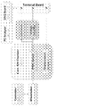
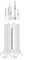
- Sensor evaluation system block diagram Controller APD-050FCA (made by Asahi Seisakusho)
- Exciter controller Wavemaker SL-0505 (manufactured by Asahi Seisakusho) shaker: Giving deformation vibration to sensor film
- IPMC sensor Ionic conductive polymer sensor film Cont.
- T / H Chamber SH-222 (manufactured by Espec) Temperature / humidity control chamber (not used in the examples, measured at room temperature and humidity in the laboratory (about 25 ° C, humidity 60) %)) Displacement Sensor IL-030 (manufactured by Keyence) Measures displacement of sensor film giving displacement vibration I / V circuit: Homemade current measurement circuit (not used in the examples) Voltage Amplifier: Homemade voltage amplification circuit Terminal Board, DAQ Board, Lab View Measurement System (NationalsInstrument) The schematic diagram when the deformation
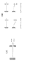
- Sensor film A Schematic diagram of fixing sensor film by holder
- B (a) Schematic diagram of fixing sensor film (1) firmly by holder (2) and applying displacement
- b) Schematic diagram when the sensor film is loosely fixed with a holder and displacement is applied
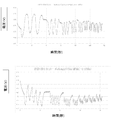
- the sensor signal of Example 1 is shown.
- the structure of the deformation sensor manufactured in Example 2 is shown.
- transformation sensor obtained in Example 2 is shown.
- transformation sensor obtained in Example 3 is shown.
- transformation sensor obtained in Example 4 is shown.
- An example of the synthetic scheme of the copolymer (MPNS) of a cationic monomer and an anionic monomer is shown.
- APS is a thermal polymerization catalyst ammonium persulfate (indicating ammonium peroxodisulfate).
- transformation sensor of this invention is shown.
- transformation sensor is shown.
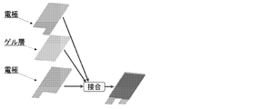
- a method for manufacturing a deformation sensor will be described.
- transformation sensor of this invention is shown.
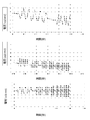
- the measurement result of the deformation amount of the deformation sensor of the present invention is shown.
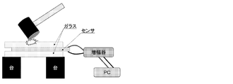
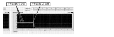
- the glass breakage detection method is shown.
- the glass breakage detection result is shown.
- examples of the ion conductive polymer include an ion exchange resin having a fluororesin skeleton or a hydrocarbon resin skeleton such as polyethylene, polypropylene, and polystyrene, a polymer complex gel, and a copolymer of a cationic monomer and an anionic monomer.
- a polymer is mentioned.
- the ion exchange resin may be any of an anion exchange resin, a cation exchange resin, and an amphoteric ion exchange resin, but a cation exchange resin is preferred.
- an ion conductive polymer having a structure in which an acidic functional group such as a sulfonic acid group or a carboxyl group is introduced into a fluororesin skeleton or a hydrocarbon resin skeleton is preferably exemplified.
- an acidic functional group such as a sulfonic acid group or a carboxyl group
- examples thereof include cation exchange resins into which acidic functional groups such as acid groups and carboxyl groups have been introduced.
- Specific examples of the cation exchange resin include perfluorosulfonic acid resins such as Nafion (registered trademark, manufactured by DuPont) membrane.
- Examples of the cation bonded to the sulfonic acid group and the carboxyl group include alkali metal ions such as H + , Na + , K + and Li + , NH 4 + and the like.
- an ion conductive polymer having a structure in which a basic functional group such as a quaternary ammonium group (for example, tetramethylammonium, tetraethylammonium) is introduced into a fluororesin skeleton or a hydrocarbon resin skeleton is preferable.
- An anion exchange resin in which a basic functional group such as a quaternary ammonium group is introduced into the fluororesin is preferable.
- the anion bonded to the quaternary ammonium group include halogen ions such as OH ⁇ and chlorine ions, and nitrate ions.
- the amphoteric ion exchange resin is an ion conductive polymer having a structure in which an acidic functional group such as a sulfonic acid group or a carboxyl group and a basic functional group such as a quaternary ammonium group are introduced into a fluororesin skeleton or a hydrocarbon resin skeleton.
- Preferred examples include amphoteric ion exchange resins in which an acidic functional group such as a sulfonic acid group or a carboxyl group and a basic functional group such as a quaternary ammonium group are introduced into a fluororesin.
- An anion exchange resin and a cation exchange resin may be used in combination.
- a polymer complex gel is a composite gel in which a polycationic polymer and a polyanionic polymer are electrostatically combined to form a composite gel, and a copolymer of a cationic monomer and an anionic monomer is bonded to each other. It has become.
- the polycationic polymer and the polyanionic polymer may be mixed at an equivalent ratio of 1: 1 so that the charge is neutralized, or one of them may be contained in excess.
- Examples of the cationic group of the polycationic polymer include ammonium or quaternary ammonium obtained by adding a proton to a primary, secondary, or tertiary amine.
- the anionic group of the polyanionic polymer include SO 3 ⁇ , COO —, and the like.
- Polycationic polymers include basic polymers such as polylysine, polyarginine, polyhistidine, homopolymers and copolymers of basic amino acids such as lysine and arginine copolymers, collagen, ionene, chitosan, aminated cellulose
- Basic vinyl polymers such as saccharides, polyvinylamine, polyallylamine, polydivinylpyridine, and salts thereof (hydrochloride, nitrate, sulfate, etc.), polyimide, polyethyleneimine, polyallylamine, polydiallyldimethylammonium salt, etc.
- the polyanionic polymer is not particularly limited as long as it is an organic polymer having an anionic substituent on the polymer chain.
- polyanionic polymers such as polyacrylic acid, polymethacrylic acid, polymaleic acid and polyaspartic acid can be used.
- Anions; Anionic polysulfonic acid such as Li styrene sulfonic acid and polyvinyl sulfonic acid.
- These polycarboxylic acid and polysulfonic acid may be a copolymer of vinyl carboxylic acid and vinyl sulfonic acid and other polymerizable monomers (such as acrylic ester and styrene).
- the cationic monomer includes (acryloylamino) alkyl-N, N, N-trialkylammonium halide, (methacryloylamino) alkyl-N, N, N-trialkyl.
- Ammonium halides, vinyl-N, N, N-trialkylammonium halides, allyl-N, N, N-trialkylammonium halides, quaternized vinylimidazoles and the like are listed.
- anionic monomers include acrylic acid and methacrylic acid.
- the molar ratio of the cationic monomer to the anionic monomer is preferably 2: 8 to 8: 2, more preferably 3: 7 to 7: 3, further preferably 4: 6 to 6: 4, and most preferably 5: 5. It is.
- Preferred copolymers of cationic monomers and anionic monomers include poly (3- (methacryloylamino) propyltrimethylammonium chloride-sodium styrenesulfonate) (MPNS), poly (dimethylaminoethyl acrylate benzyl chloride) -P-sodium styrene sulfonate copolymer (DMNS) is shown in Fig. 8.
- a synthesis scheme of MPNS is shown in Fig. 8.
- a deformation sensor of the present invention is schematically shown in Fig. 9.
- the thickness of the ion conductive polymer layer is about 25 to 500 ⁇ m.
- two or more flexible electrodes can be used to sandwich the ion conductive polymer layer, and preferably a pair of flexible electrodes can be used.
- the electrode include a metal flat plate, a metal thin film (for example, a metal foil such as SUS foil and aluminum foil), a transparent electrode (for example, an ITO film), a nanocarbon thin film (for example, a carbon nanotube thin film), and a plastic electrode.
- the electrode material is preferably a transparent conductive substrate (for example, a film), but a metal flat plate, a metal thin film, or a nanocarbon thin film can be used for applications where transparency is not required.
- the electrode using a transparent conductive substrate includes a plastic electrode and a transparent electrode. When using a metal flat plate, a metal thin film, a metal foil, etc. as an electrode, you may laminate a protective film.
- the deformation sensor of the present invention can operate in air, in water, in vacuum, or in an organic solvent, and may be appropriately sealed depending on the use environment. There is no restriction
- the electrode may be a flexible printed substrate on which wiring is written by a technique such as etching.
- a printed substrate is effective when a plurality of sensors are provided on a single substrate.
- you may provide a nonelectroconductive part in a part of electrode in order to prevent the short circuit by contact between electrodes.
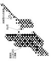
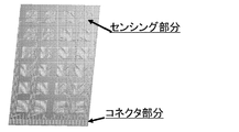
- FIG. 10 shows a deformation sensor of the present invention having a plurality of sensing portions.
- a deformation sensor having a large number of sensing portions can be obtained by (Step 1) printing the pattern of the transparent electrode on the transparent plate, scraping the surface of the transparent plate coated with the transparent electrode, or treating the pattern with an acid base.
- Step 2) Prepare two or more transparent electrodes having a pattern electrode, sandwich an ionic conductive polymer (FIG. 11), (Step 3) wire the transparent electrode, and use it as a deformation sensor. It can be obtained by the following three steps.
- the sensing part is preferably transparent.
- plastic electrodes include those obtained by laminating a plastic layer and a conductive film.
- plastics include acrylic resins such as polymethyl methacrylate (PMMA) and polymethyl acrylate (PMA), polyethylene (PE), polypropylene (PP), polyethylene terephthalate (PET), polyethylene-2,6-naphthalate, polypropylene terephthalate, Nylon 6, Nylon 4, Nylon 66, Nylon 12, Polyimide, Polyamideimide, Polyethersulfone, Polyetheretherketone, Polycarbonate, Polyethylene naphthalate (PEN), Polyethylene butyrate, Polyarylate, Triacetylcellulose, Cellulose propionate , Polyvinyl chloride, polyvinylidene chloride, polyvinyl alcohol, polyetherimide, polyphenylene sulfide, polyphenylene ox Id, polystyrene, syndiotactic polystyrene, norbornene polymer, cycloolefin polymer (COP), a transparent plastic such as cycloolefin copolymer (C
- the conductive film examples include a laminate of an inorganic semiconductor film, a conductive polymer film, a metal mesh, and a nanocarbon thin film.
- the conductive film is preferably transparent.
- the conductive film is an inorganic semiconductor film, evaporation of water, carbonate (ethylene carbonate, propylene carbonate, etc.) and other organic solvents contained in the ion conductive polymer layer is suppressed (water vapor impermeable or organic Solvent impermeability) and the influence of water vapor in the air can be suppressed.
- the inorganic semiconductor examples include one or more oxides (including complex oxides) such as titanium, tin, zinc, tungsten, zirconium, gallium, indium, yttrium, niobium, tantalum, and vanadium, preferably Metal oxide semiconductors such as tin oxide, indium oxide, and zinc oxide, laminated conductive films in which silver thin films or gold thin films are laminated with a high refractive dielectric, tin-doped indium oxide (ITO), fluorine-doped tin oxide (FTO), etc. Can be mentioned.
- oxides including complex oxides
- metal oxide semiconductors such as tin oxide, indium oxide, and zinc oxide
- laminated conductive films in which silver thin films or gold thin films are laminated with a high refractive dielectric tin-doped indium oxide (ITO), fluorine-doped tin oxide (FTO), etc.
- ITO tin-doped indium oxide
- FTO fluor
- the conductive polymer examples include polythiophene-based, polyacetylene-based, polyparaphenylene-based, polyaniline-based, polyparaphenylene vinylene-based, and polypyrrole-based polymers.
- Polystyrene sulfonic acid (PPS) is preferable as a transparent conductive polymer.
- PPS Polystyrene sulfonic acid
- PVS polyvinyl sulfonic acid
- TsO p-toluenesulfonic acid
- Examples of the metal of the metal mesh include platinum, gold, silver, nickel, etc. Silver and nickel are preferable from the viewpoint of economy, and silver is most preferable from the viewpoint of excellent conductivity.
- nanocarbon thin film examples include thin films such as carbon nanotubes, carbon nanohorns, carbon nanofibers, and graphite nanocrystals, and a laminate of two or more of these thin films.
- the conductive film is preferably transparent.
- a preferable transparent conductive film is desirably one having a surface resistance of 100 ⁇ / ⁇ or less and having a water vapor barrier performance.
- Preferred materials include a three-layer structure (ITO / Ag / ITO) in which a silver thin film is sandwiched between ITO films, and five layers. The configuration ((ITO / Ag / ITO / Ag / ITO)) is used. In order to obtain high visible light transmittance and low surface resistance, a multilayer structure is desirable.
- the transparent conductive film Altair-M-5, 10, 20, etc. sold by Mitsui Chemicals, TCO film used for EMI shield filter for plasma display, etc. can be used.
- a laminated structure of a transparent barrier film and a conductive film in which a metal such as silver or copper is meshed may be used.
- a transparent barrier film a silica film, a SiON film, or the like can be used.
- Each electrode such as a plastic electrode is provided with a lead wire so that a sensor signal can be taken out.
- the thickness of the plastic layer is about 12 to 200 ⁇ m, and the thickness of the conductive film is about 0.03 to 3 ⁇ m.
- deformations that cause non-uniform ion distribution include bending, twisting, breaking, pressing, dents, and bending.
- the ion conductive polymer layer and the electrode may be joined by pressure bonding, hot pressing or the like, or may be adhered by an adhesive. Moreover, you may stick with a double-sided tape, and you may fix with a bolt nut.
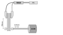
- Measurement Method Sensor characteristics were measured using the measurement system shown in FIG. Fix the sensor film (deformation sensor) to the electrode in the chamber, and fix it as shown in Fig. 2 (B) (a) and (b) using the holder shown in Fig. 1 (B) connected to the vibrator. Then, vibration was applied using a vibrator and the generated voltage signal was measured. In the examples, measurement was performed at room temperature and humidity in the laboratory without using Cont. T / H Chamber SH-222 (manufactured by Espec) (about 25 ° C., humidity about 60%). Also, an I / V circuit (homemade current measurement circuit) is not used in the examples.
- Example 1 Sensor voltage characteristics of a bonded body obtained by electroless plating of Nafion on Nafion Nafion 117 membrane (charge density 0.91 mequiv./g, dry thickness 175 ⁇ m) shown below (N117)
- a gold electrode was prepared by electroless plating. Electroless plating was performed according to the method described in Japanese Patent No. 2961125. The gold electrode was joined by immersing the N117 film in an aqueous solution of gold chloride phenanthroline complex ([Au (phen) Cl 2 ] + ), adsorbing the complex ions, and then reducing in a sodium sulfite aqueous solution. This process was repeated 5 times, plated, and then immersed in 0.1 M NaOH for one day or more to convert counter ions to Na, and then stored in pure water. The peripheral portion of the electroless gold-plated thin film was cut to obtain a deformation sensor of the present invention.
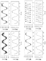
- Fig. 3 shows the sensor signal when a deformation of ⁇ 2mm and a frequency of 0.1Hz to 2Hz is applied to the deformation sensor of the present invention in which N117 is gold-plated. A voltage signal of about 1 mVp-p was observed.
- Example 2 Sensor voltage characteristics of Nafion / ITO film assembly
- Two plastic electrodes surface resistance 10 ⁇ / ⁇ , ITO / Ag / ITO, or ITO / laminated with PET film (plastic film) and ITO film (conductive film) Ag / ITO / Ag / ITO (manufactured by Mitsui Chemicals, Inc.) and one Nafion N117 membrane were attached to both sides of the N117 membrane using a double-sided tape (FIG. 4).
- the N117 membrane was stored by immersing it in pure water with the counter ion in the form of sodium.
- the N117 membrane (5 mm x 30 mm) was taken out of the pure water and the surface water was removed.
- a hole of 5 mm ⁇ 30 mm is made in a double-sided tape of 45 mm ⁇ 15 mm, the N117 film is put, and an ITO film of a plastic electrode is bonded to both sides of the double-sided tape.
- the ITO film (conductive film) side of the plastic electrode was directed to the N117 film side so that the conductive film and the N117 film were sufficiently adhered.
- the aluminum foil was used for taking out the lead wire from the ITO film as shown in FIG.
- FIG. 5 shows sensor signals when a vibration with a frequency of 0.1 Hz to 10 Hz is applied with a displacement of ⁇ 2 mm. Although the cause is unknown at present, a signal of about 80 mVp-p at maximum, which is larger than that of Example 1, was obtained.
- Example 3 Sensor Voltage Characteristics of Plastic Electrode / Nafion Thin Film / Plastic Electrode Assembly Nafion Dispersion Solution on Plastic Electrode ITO Film (15 mm x 44 mm) (Surface Resistance 30 ⁇ / ⁇ ) Composed of ITO Film and PET Film (Wako Pure Chemicals DE1020, Nafion 10wt%, water 90wt%) and apply the same size plastic electrode (PET film / ITO film) with the ITO film side facing the Nafion dispersion layer at 70 ° C and 200 N
- a 3.5 hour hot press was performed to produce a (PET film / ITO film)-(Nafion thin film)-(ITO film / PET film) joined body, and then immersed in pure water for more than one day and night.
- the sensor characteristics were measured under the same conditions. In this case, the counter ion is a hydrogen ion. The measurement results are shown in FIG. Signals between 2 mVp-p and 3 mVp-
- Example 4 Sensor Voltage Characteristics of Plastic Electrode / Polymer Complex Gel Film / Plastic Electrode Assembly Polymer complex gel (cationic monomer: 3 (methacryloylamino) propyltrimethylammonium chloride, anionic monomer: co-polymerization with sodium parastyrene sulfonate
- the two plastic electrodes (PET film / ITO film) used in Example 3 were placed on both sides of the unitary gel (MPNS) and Mitsui Chemicals Co., Ltd. film so that the ITO film sandwiched the polymer complex gel film.
- Example 5 Two stainless steel plates of 0.2 mm thickness and 10 mm ⁇ 40 mm and ion conductive gel (MPNS-Na, MPNS-Li, DMNS-Na, or DMNS-Li) were used. The two stainless plates were placed so that the gel was sandwiched between them, and they were crimped by a press to obtain a deformation sensor. The press pressure was 500N for 3 hours. After pressure bonding, it was laminated with a protective film.
- MPNS-Na, MPNS-Li, DMNS-Na, or DMNS-Li ion conductive gel
- ⁇ Wiring was performed on each of the two stainless steel plates in the deformation sensor.
- the wiring was connected to an amplifier, and the amplified sensor signal was measured in the Labview environment (FIG. 12).
- an amplification factor of 10 ⁇ 4 or more is desirable for voltage measurement
- an amplification factor of 10 ⁇ 6 or more is desirable for current measurement.
- the displacement of the shaker is converted into the curvature of the sensor, and a signal corresponding to the curvature is output.
- a vibration with a frequency of 0.1 to 10 Hz and an amplitude of 2 mm was applied to a position 28 mm from the sensor clamp.
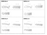
- the gels used were the following four types. High Tg gel Na ion (MPNS-Na) High Tg gel Li substitution (MPNS-Li) Low Tg gel Na ion (DMNS-Na) Low Tg gel Li substitution (DMNS-Li) The measurement results of each gel (ion conductive polymer layer) are shown in FIG.
- Example 6 As shown in FIG. 14, the deformation sensor obtained in Example 5 and glass were set, and an impact that did not break the glass with a hammer was applied three times, and another impact that caused the glass to break was applied once. As a result, a clearly different signal was obtained when the glass was broken and when it was not broken (FIG. 15).
Landscapes
- Physics & Mathematics (AREA)
- General Physics & Mathematics (AREA)
- Chemical & Material Sciences (AREA)
- Dispersion Chemistry (AREA)
- Spectroscopy & Molecular Physics (AREA)
- Measurement Of Length, Angles, Or The Like Using Electric Or Magnetic Means (AREA)
Abstract
Description
項1. イオン導電性高分子層を柔軟な電極で挟んだ構造を有し、変形によりイオン導電性高分子層内に不均一なイオン分布が生じて、電極間に電位差が生じることを特徴とする、変形センサー。
項2. 前記電極の電極材料が透明導電基材又は金属箔である、項1に記載の変形センサー。
項3. 前記電極がプラスチック電極である、項1に記載の変形センサー。
項4. プラスチック電極が水蒸気非透過性である、項3に記載の変形センサー。
項5. 前記プラスチック電極がプラスチック層と導電膜を含み、導電膜でイオン導電性高分子層を挟む構造を有し、前記導電膜が無機半導体、導電性高分子、金属メッシュ及びナノカーボン薄膜の積層体からなる群から選ばれる、項1~4のいずれか1項に記載の変形センサー。
項6. 前記導電膜がITOフィルムである、項5に記載の変形センサー。
項7. イオン導電性高分子がイオン交換樹脂を含む、項1~6のいずれか1項に記載の変形センサー。
項8. イオン導電性高分子がポリマーコンプレックスゲルを含む、項1~6のいずれか1項に記載の変形センサー。
*測定法
センサー特性の測定は、図1(A)に示した測定システムを用いて行った。センサーフィルム(変形センサー)をチャンバー内の電極に固定、加振器につながった図1(B)に示すホルダーを用いて、図2(B)(a)、(b)に示す様に固定し、加振器を用いて振動を加え、発生する電圧信号を測定した。なお、実施例では、Cont. T/H Chamber SH-222 (エスペック社製)を用いずに、実験室内の室温、湿度で測定した(約25℃、湿度60%程度)。また、I/V circuit(自家製電流測定回路)は、実施例では用いていない。
下記に示すデュポン社のナフィオン117膜(荷電密度0.91 mequiv./g, 乾燥厚み175μm)(N117)

PETフィルム(プラスチックフィルム)とITOフィルム(導電膜)を積層した2つのプラスチック電極(表面抵抗10 Ω/□、ITO/Ag/ITO、又はITO/Ag/ITO/Ag/ITO、三井化学株式会社製)と1つのナフィオンN117膜を、両面テープを用いてN117膜の両面に貼り付けた(図4)。N117 膜は、実施例1と同様、カウンターイオンがナトリウムにした状態で、純水中に浸して保存したものを用い、純水中からN117 膜(5mm×30mm)を取り出して、表面の水を拭き取った後、45mm×15mmの大きさの両面テープに5mm×30mmの穴をあけて、前記N117膜を入れ、両面テープの両側にプラスチック電極のITOフィルムを接着する。その際、プラスチック電極のITOフィルム(導電膜)側をN117膜側に向け、導電膜とN117 膜が十分接着するようにした。また、ITOフィルムからのリード線の取出しは、図4に示す様にアルミ箔を用いた。
ITOフィルムとPETフィルムから構成されるプラスチック電極のITOフィルム(15 mm x 44 mm)(表面抵抗30Ω/□)にナフィオンディスパージョン溶液(和光純薬DE1020,ナフィオン10wt%, 水90wt%)を塗布し、同じサイズのプラスチック電極(PETフィルム/ITOフィルム)のITOフィルム側をナフィオンディスパージョン層に向けて重ね、70 ℃、200 Nで3.5 時間ホットプレスを行うことで、(PETフィルム/ITOフィルム)-(ナフィオン薄膜)-(ITOフィルム/PETフィルム)接合体を作製し、その後、純水に1昼夜以上浸した後、実施例1と同様の条件でセンサー特性の測定を行った。この場合、カウンターイオンは水素イオンである。測定の結果を図6に示す。2 mVp-p~3 mVp-pの信号を得た。
ポリマーコンプレックスゲル(カチオン性モノマー:3(メタクリロイルアミノ)プロピルトリメチルアンモニウムクロリド、アニオン性モノマー:パラスチレンスルホン酸ナトリウムとの共重合体からなるゲル(MPNS)、三井化学株式会社製)フィルムの両面に実施例3で用いた2つのプラスチック電極(PETフィルム/ITOフィルム)を、そのITOフィルムがポリマーコンプレックスゲルフィルムを挟むように重ね合わせ、プレスで圧着(常温、500 N、30分)し、(PETフィルム/ITOフィルム)-(ポリマーコンプレックスゲルフィルム)-(ITOフィルム/PETフィルム)接合体を作製し、実施例2と同様の条件でセンサー特性の測定を行った。この場合、カウンターイオンはナトリウムイオン、および、塩素イオンであった。測定の結果を図7に示す。0.2mVp-p~0.4mVp.pの信号を得た。
0.2mm厚10mm×40mmのステンレス板2枚とイオン導電性ゲル(MPNS-Na、MPNS-Li、DMNS-Na、又は、DMNS-Li)を用いた。2枚のステンレス板でゲルを挟みこむように配置し、それらをプレス機によって圧着して、変形センサーを得た。プレス圧は500Nで3時間であった。圧着後、保護フィルムでラミネートした。
高TgゲルNaイオン(MPNS-Na)
高TgゲルLi置換 (MPNS-Li)
低TgゲルNaイオン (DMNS-Na)
低TgゲルLi置換 (DMNS-Li)
各ゲル(イオン導電性高分子層)の計測結果を図13及び表1に示す。
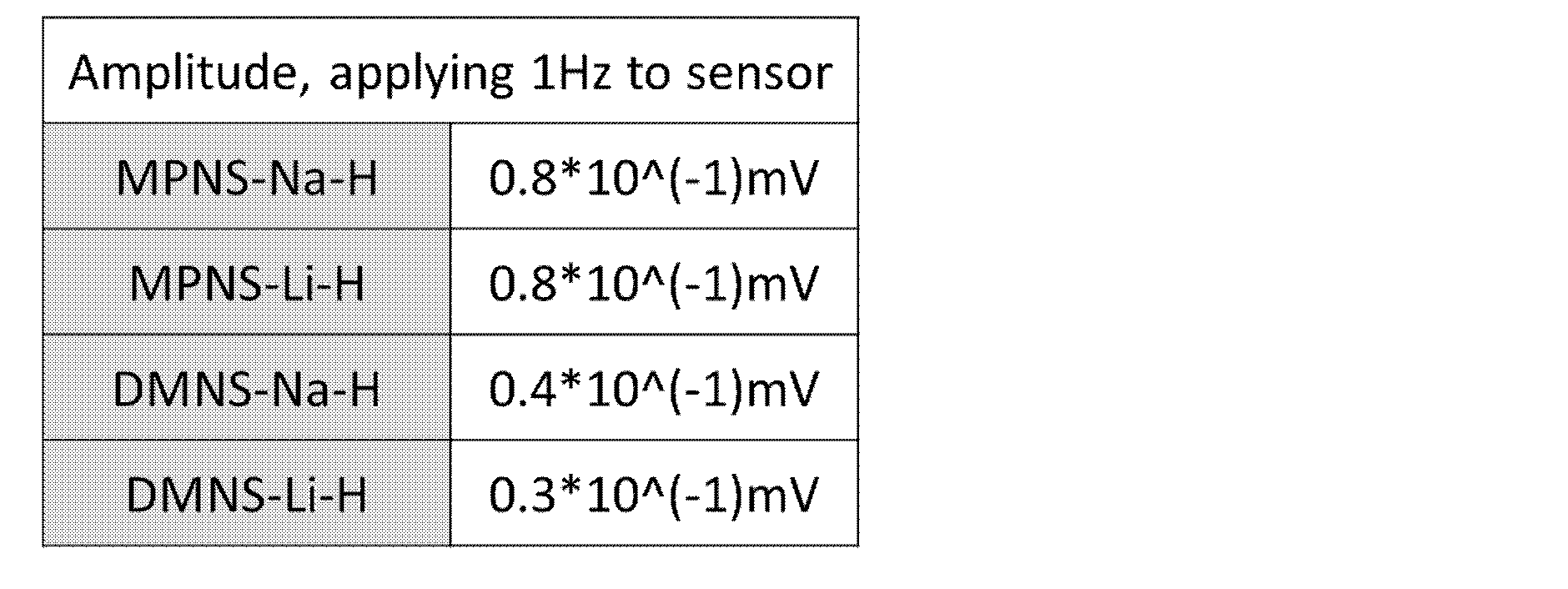
図14に示すように実施例5で得られた変形センサーとガラスをセットして、ハンマーでガラスが割れない程度の衝撃を3回、さらにガラスが割れる程度の衝撃を1回加えた。その結果、ガラス破壊時と非破壊時に明らかに異なる信号を取得できた(図15)。
2 ホルダ
3 プラスチック層(PETフィルム)
4 導電膜(ITOフィルム)
5 プラスチック電極
6 イオン導電性高分子(N117)
7 両面テープ
8 アルミホイル
Claims (8)
- イオン導電性高分子層を柔軟な電極で挟んだ構造を有し、変形によりイオン導電性高分子層内に不均一なイオン分布が生じて、電極間に電位差が生じることを特徴とする、変形センサー。
- 前記電極の電極材料が透明導電基材又は金属箔である、請求項1に記載の変形センサー。
- 前記電極がプラスチック電極である、請求項1に記載の変形センサー。
- プラスチック電極が水蒸気非透過性である、請求項3に記載の変形センサー。
- 前記プラスチック電極がプラスチック層と導電膜を含み、導電膜でイオン導電性高分子層を挟む構造を有し、前記導電膜が無機半導体、導電性高分子、金属メッシュ及びナノカーボン薄膜の積層体からなる群から選ばれる、請求項1~4のいずれか1項に記載の変形センサー。
- 前記導電膜がITOフィルムである、請求項5に記載の変形センサー。
- イオン導電性高分子がイオン交換樹脂を含む、請求項1~6のいずれか1項に記載の変形センサー。
- イオン導電性高分子がポリマーコンプレックスゲルを含む、請求項1~6のいずれか1項に記載の変形センサー。
Priority Applications (5)
| Application Number | Priority Date | Filing Date | Title |
|---|---|---|---|
| KR1020187020617A KR20180097658A (ko) | 2015-12-25 | 2016-12-22 | 변형 센서 |
| JP2017558258A JP6829358B2 (ja) | 2015-12-25 | 2016-12-22 | 変形センサー |
| US16/064,121 US10788307B2 (en) | 2015-12-25 | 2016-12-22 | Deformation sensor comprising an ion-conductive polymer layer |
| CN201680071436.7A CN108369085A (zh) | 2015-12-25 | 2016-12-22 | 变形传感器 |
| EP16878891.7A EP3396305A4 (en) | 2015-12-25 | 2016-12-22 | STRAIN SENSOR |
Applications Claiming Priority (2)
| Application Number | Priority Date | Filing Date | Title |
|---|---|---|---|
| JP2015253911 | 2015-12-25 | ||
| JP2015-253911 | 2015-12-25 |
Publications (1)
| Publication Number | Publication Date |
|---|---|
| WO2017111004A1 true WO2017111004A1 (ja) | 2017-06-29 |
Family
ID=59090474
Family Applications (1)
| Application Number | Title | Priority Date | Filing Date |
|---|---|---|---|
| PCT/JP2016/088351 Ceased WO2017111004A1 (ja) | 2015-12-25 | 2016-12-22 | 変形センサー |
Country Status (6)
| Country | Link |
|---|---|
| US (1) | US10788307B2 (ja) |
| EP (1) | EP3396305A4 (ja) |
| JP (1) | JP6829358B2 (ja) |
| KR (1) | KR20180097658A (ja) |
| CN (1) | CN108369085A (ja) |
| WO (1) | WO2017111004A1 (ja) |
Cited By (3)
| Publication number | Priority date | Publication date | Assignee | Title |
|---|---|---|---|---|
| CN108981976A (zh) * | 2018-08-14 | 2018-12-11 | 深圳大学 | 一种柔性电容式应力传感器芯片及其制备方法 |
| CN109141696A (zh) * | 2018-07-31 | 2019-01-04 | 上海材料研究所 | 一种基于压电薄膜的柔性触觉传感器及其信号处理系统 |
| JP2023529491A (ja) * | 2020-06-12 | 2023-07-10 | リキッド ワイヤ インコーポレイテッド | 多軸差動歪みセンサ |
Families Citing this family (16)
| Publication number | Priority date | Publication date | Assignee | Title |
|---|---|---|---|---|
| KR101993313B1 (ko) | 2019-04-15 | 2019-06-26 | 한국생산기술연구원 | 액체 금속을 이용한 유연성 필터 소자 및 그 제조 방법 |
| KR101993314B1 (ko) | 2019-04-16 | 2019-06-26 | 한국생산기술연구원 | 액체 금속을 포함하는 기판 적층체, 이를 이용한 유연성 필터 소자 및 필터 소자의 제조 방법 |
| KR102569329B1 (ko) | 2019-04-16 | 2023-08-22 | 한국생산기술연구원 | 액체 금속을 이용한 유연성 센서 디바이스 |
| KR102322963B1 (ko) | 2019-04-17 | 2021-11-09 | 한국생산기술연구원 | 액체 금속이 침습된 베이스를 포함하는 도전성 패턴 기판 |
| KR102013796B1 (ko) | 2019-05-27 | 2019-10-21 | 한국생산기술연구원 | 액체 금속을 이용한 도전성 패턴 기판 및 그 제조 방법 |
| KR102478313B1 (ko) | 2019-05-28 | 2022-12-16 | 한국생산기술연구원 | 핀을 이용한 도전성 패턴의 제조 방법 및 그로부터 제조된 패턴 기판 |
| KR102035581B1 (ko) | 2019-05-28 | 2019-10-23 | 한국생산기술연구원 | 도전성 패턴 형성용 스탬프, 이를 이용한 도전성 패턴 기판의 제조 방법 및 이를 통해 준비된 도전성 패턴 기판 |
| KR102317316B1 (ko) | 2019-06-03 | 2021-10-26 | 한국생산기술연구원 | 스탬프를 이용한 액체 금속의 패터닝 방법 |
| KR102078215B1 (ko) | 2019-06-19 | 2020-02-17 | 한국생산기술연구원 | 액체 금속을 포함하는 인덕터 복합 소자, 인덕터 복합 소자를 포함하는 수동 소자 기판의 제조 방법, 및 수동 소자 기판의 튜닝 방법 |
| KR102063802B1 (ko) | 2019-06-19 | 2020-01-08 | 한국생산기술연구원 | 개선된 기생 커패시턴스 특성을 갖는 액체 금속 커패시터 복합 소자 기판 및 그 제조 방법 |
| KR20210004063A (ko) | 2019-07-03 | 2021-01-13 | 한국생산기술연구원 | 커패시터 복합 소자 기판 |
| KR20210004059A (ko) | 2019-07-03 | 2021-01-13 | 한국생산기술연구원 | 인덕터 복합 소자 기판 |
| JP2023513046A (ja) | 2020-01-30 | 2023-03-30 | リクイッド エックス プリンティッド メタルズ インコーポレイテッド | 力センサ制御式伝導加熱素子 |
| CN112629399B (zh) * | 2020-11-24 | 2022-04-22 | 南京航空航天大学 | 一种聚氯乙烯离子凝胶的柔性传感元件及其制备方法 |
| MX2023014190A (es) * | 2021-05-28 | 2024-04-10 | Liquid X Printed Metals Inc | Sensores de fuerza, electronica controlada por sensor de fuerza, y elementos de calentamiento conductores controlados por sensor de fuerza. |
| CN113603819A (zh) * | 2021-06-03 | 2021-11-05 | 福建师范大学 | 一种基于MXenes纳米片复合聚电解质水凝胶的柔性可穿戴传感器的制备方法 |
Citations (10)
| Publication number | Priority date | Publication date | Assignee | Title |
|---|---|---|---|---|
| JPH0381909A (ja) * | 1989-08-25 | 1991-04-08 | Matsushita Electric Ind Co Ltd | 電気化学素子のレドックス反応極用材料 |
| JPH06223838A (ja) * | 1993-01-25 | 1994-08-12 | Meidensha Corp | 亜鉛−臭素電池の集電電極 |
| US20030034534A1 (en) * | 1999-06-04 | 2003-02-20 | Mrinal Thakur | Sensor apparatus using an electrochemical cell |
| JP2005039995A (ja) * | 2003-06-26 | 2005-02-10 | Eamex Co | 可撓性素子及びその用途 |
| JP2006172722A (ja) * | 2004-12-10 | 2006-06-29 | Toin Gakuen | 塗膜形成用組成物、それを用いて得られる電極及び光電変換素子 |
| JP2007096049A (ja) * | 2005-09-29 | 2007-04-12 | Sumitomo Osaka Cement Co Ltd | 光学フィルター及びその製造方法 |
| JP2007128280A (ja) * | 2005-11-04 | 2007-05-24 | Shin Etsu Polymer Co Ltd | 座標入力装置用導電シート並びにその製造方法及び座標入力装置 |
| JP2008153026A (ja) * | 2006-12-15 | 2008-07-03 | Kuraray Luminas Co Ltd | 分散型無機エレクトロルミネッセンス素子およびこれを備える照明装置 |
| JP2012032325A (ja) * | 2010-08-02 | 2012-02-16 | Sony Corp | 形状センサおよび情報入力装置 |
| JP2014201800A (ja) * | 2013-04-05 | 2014-10-27 | リンテック株式会社 | 透明導電フィルム、および透明導電フィルムの形成方法 |
Family Cites Families (13)
| Publication number | Priority date | Publication date | Assignee | Title |
|---|---|---|---|---|
| US5672937A (en) * | 1996-06-12 | 1997-09-30 | Choi; Kue Byung | Light-transmitting electroconductive plastic film electrodes and method of manufacture |
| JP2006153950A (ja) | 2004-11-25 | 2006-06-15 | Sumitomo Osaka Cement Co Ltd | 光学フィルター |
| JP5110574B2 (ja) | 2007-06-25 | 2012-12-26 | 独立行政法人産業技術総合研究所 | 高アスペクト比のカーボンナノチューブとイオン液体から構成される導電性薄膜、アクチュエータ素子 |
| JP4784840B2 (ja) | 2007-11-30 | 2011-10-05 | 独立行政法人産業技術総合研究所 | 磁場応答固体高分子複合体およびアクチュエータ素子 |
| CN101925793A (zh) * | 2008-01-28 | 2010-12-22 | 可乐丽股份有限公司 | 具有柔性的变形传感器 |
| JP5046127B2 (ja) | 2008-10-16 | 2012-10-10 | 独立行政法人産業技術総合研究所 | 高アスペクト比のカーボンナノチューブとイオン液体から構成される導電性薄膜、アクチュエータ素子 |
| JP5083911B2 (ja) | 2009-01-08 | 2012-11-28 | 独立行政法人産業技術総合研究所 | カーボンナノチューブと重合性イオン液体およびイオン液体から構成されるアクチュエータ素子 |
| WO2010095581A1 (ja) * | 2009-02-18 | 2010-08-26 | 株式会社クラレ | マルチ積層変形センサ |
| TWI448935B (zh) * | 2011-05-20 | 2014-08-11 | Nat Univ Tsing Hua | 三維觸控單元及三維觸控面板 |
| CN202193728U (zh) * | 2011-08-12 | 2012-04-18 | 蚌埠玻璃工业设计研究院 | 一种新型电磁屏蔽镀膜玻璃 |
| KR101557186B1 (ko) * | 2013-01-09 | 2015-10-05 | (주)엘지하우시스 | 투명 수지 적층체 및 이를 포함하는 터치 스크린 패널 |
| JP6421430B2 (ja) * | 2014-03-31 | 2018-11-14 | デクセリアルズ株式会社 | ポリマー素子、電子機器、カメラモジュールおよび撮像装置 |
| JP2015197409A (ja) * | 2014-04-03 | 2015-11-09 | セイコーエプソン株式会社 | 圧力分布センサー、圧力分布測定方法およびロボットハンド |
-
2016
- 2016-12-22 EP EP16878891.7A patent/EP3396305A4/en not_active Withdrawn
- 2016-12-22 JP JP2017558258A patent/JP6829358B2/ja not_active Expired - Fee Related
- 2016-12-22 US US16/064,121 patent/US10788307B2/en not_active Expired - Fee Related
- 2016-12-22 WO PCT/JP2016/088351 patent/WO2017111004A1/ja not_active Ceased
- 2016-12-22 KR KR1020187020617A patent/KR20180097658A/ko not_active Ceased
- 2016-12-22 CN CN201680071436.7A patent/CN108369085A/zh active Pending
Patent Citations (10)
| Publication number | Priority date | Publication date | Assignee | Title |
|---|---|---|---|---|
| JPH0381909A (ja) * | 1989-08-25 | 1991-04-08 | Matsushita Electric Ind Co Ltd | 電気化学素子のレドックス反応極用材料 |
| JPH06223838A (ja) * | 1993-01-25 | 1994-08-12 | Meidensha Corp | 亜鉛−臭素電池の集電電極 |
| US20030034534A1 (en) * | 1999-06-04 | 2003-02-20 | Mrinal Thakur | Sensor apparatus using an electrochemical cell |
| JP2005039995A (ja) * | 2003-06-26 | 2005-02-10 | Eamex Co | 可撓性素子及びその用途 |
| JP2006172722A (ja) * | 2004-12-10 | 2006-06-29 | Toin Gakuen | 塗膜形成用組成物、それを用いて得られる電極及び光電変換素子 |
| JP2007096049A (ja) * | 2005-09-29 | 2007-04-12 | Sumitomo Osaka Cement Co Ltd | 光学フィルター及びその製造方法 |
| JP2007128280A (ja) * | 2005-11-04 | 2007-05-24 | Shin Etsu Polymer Co Ltd | 座標入力装置用導電シート並びにその製造方法及び座標入力装置 |
| JP2008153026A (ja) * | 2006-12-15 | 2008-07-03 | Kuraray Luminas Co Ltd | 分散型無機エレクトロルミネッセンス素子およびこれを備える照明装置 |
| JP2012032325A (ja) * | 2010-08-02 | 2012-02-16 | Sony Corp | 形状センサおよび情報入力装置 |
| JP2014201800A (ja) * | 2013-04-05 | 2014-10-27 | リンテック株式会社 | 透明導電フィルム、および透明導電フィルムの形成方法 |
Non-Patent Citations (1)
| Title |
|---|
| See also references of EP3396305A4 * |
Cited By (4)
| Publication number | Priority date | Publication date | Assignee | Title |
|---|---|---|---|---|
| CN109141696A (zh) * | 2018-07-31 | 2019-01-04 | 上海材料研究所 | 一种基于压电薄膜的柔性触觉传感器及其信号处理系统 |
| CN108981976A (zh) * | 2018-08-14 | 2018-12-11 | 深圳大学 | 一种柔性电容式应力传感器芯片及其制备方法 |
| JP2023529491A (ja) * | 2020-06-12 | 2023-07-10 | リキッド ワイヤ インコーポレイテッド | 多軸差動歪みセンサ |
| JP7815149B2 (ja) | 2020-06-12 | 2026-02-17 | リキッド ワイヤ インコーポレイテッド | 多軸差動歪みセンサ |
Also Published As
| Publication number | Publication date |
|---|---|
| JP6829358B2 (ja) | 2021-02-10 |
| EP3396305A4 (en) | 2019-08-28 |
| EP3396305A1 (en) | 2018-10-31 |
| US10788307B2 (en) | 2020-09-29 |
| CN108369085A (zh) | 2018-08-03 |
| KR20180097658A (ko) | 2018-08-31 |
| US20190003818A1 (en) | 2019-01-03 |
| JPWO2017111004A1 (ja) | 2018-10-18 |
Similar Documents
| Publication | Publication Date | Title |
|---|---|---|
| JP6829358B2 (ja) | 変形センサー | |
| Park et al. | Deformable and transparent ionic and electronic conductors for soft energy devices | |
| Niu et al. | Stretchable ionic conductors for soft electronics | |
| CN104677399B (zh) | 超声波传感器 | |
| Li et al. | Embedding silver nanowires into a hydroxypropyl methyl cellulose film for flexible electrochromic devices with high electromechanical stability | |
| KR101661043B1 (ko) | 터치 패널 및 그 제조 방법 | |
| Wu et al. | Ultrasensitive, stretchable, and transparent humidity sensor based on ion-conductive double-network hydrogel thin films | |
| KR101444132B1 (ko) | 복합 편광판 일체형 터치 감지 전극 및 이를 구비한 터치 스크린 패널 | |
| WO2009096419A1 (ja) | 可撓性を有する変形センサ | |
| Wang et al. | Highly reliable silver nanowire transparent electrode employing selectively patterned barrier shaped by self-masked photolithography | |
| US20080042996A1 (en) | Touch panel with a transparent electrically conductive polymer film and manufacturing process | |
| JP4388966B2 (ja) | 座標入力装置 | |
| WO2007058119A1 (ja) | 導電性樹脂組成物、それを用いてなる導電性フィルム、及びそれを用いてなる抵抗膜式スイッチ | |
| CN105474149A (zh) | 集成有偏光板的触摸感测电极 | |
| CN107866824A (zh) | 机器人电子皮肤 | |
| TWI580933B (zh) | 超音波感測器 | |
| KR20160094621A (ko) | 수전사용 전도성 전사필름, 이를 이용한 코팅 방법 | |
| Deng et al. | Gel electrolytes for electrochemical actuators and sensors applications | |
| KR20070042506A (ko) | 터치패널용 복합 투명도전성 기재 및 터치패널 | |
| JP2016087963A (ja) | 透明導電体及びタッチパネル | |
| CN203930768U (zh) | 触控面板 | |
| Chen et al. | Stretchable and robust silver nanowire composites on transparent butyl rubber | |
| CN214623615U (zh) | 一种透明电阻式压力传感器 | |
| KR20160005221A (ko) | 폴리이미드 유기 유전층을 포함한 정전기력 기반 작동기 | |
| JP2007172984A (ja) | 有機導電膜、透明有機導電フィルム及び座標入力装置 |
Legal Events
| Date | Code | Title | Description |
|---|---|---|---|
| 121 | Ep: the epo has been informed by wipo that ep was designated in this application |
Ref document number: 16878891 Country of ref document: EP Kind code of ref document: A1 |
|
| ENP | Entry into the national phase |
Ref document number: 2017558258 Country of ref document: JP Kind code of ref document: A |
|
| NENP | Non-entry into the national phase |
Ref country code: DE |
|
| ENP | Entry into the national phase |
Ref document number: 20187020617 Country of ref document: KR Kind code of ref document: A |
|
| WWE | Wipo information: entry into national phase |
Ref document number: 1020187020617 Country of ref document: KR |
|
| WWE | Wipo information: entry into national phase |
Ref document number: 2016878891 Country of ref document: EP |
|
| ENP | Entry into the national phase |
Ref document number: 2016878891 Country of ref document: EP Effective date: 20180725 |