WO2017115537A1 - プラグ側コネクタ、レセプタクル側コネクタおよび電子機器 - Google Patents
プラグ側コネクタ、レセプタクル側コネクタおよび電子機器 Download PDFInfo
- Publication number
- WO2017115537A1 WO2017115537A1 PCT/JP2016/080967 JP2016080967W WO2017115537A1 WO 2017115537 A1 WO2017115537 A1 WO 2017115537A1 JP 2016080967 W JP2016080967 W JP 2016080967W WO 2017115537 A1 WO2017115537 A1 WO 2017115537A1
- Authority
- WO
- WIPO (PCT)
- Prior art keywords
- side connector
- receptacle
- plug
- ground electrode
- impedance
- Prior art date
- Legal status (The legal status is an assumption and is not a legal conclusion. Google has not performed a legal analysis and makes no representation as to the accuracy of the status listed.)
- Ceased
Links
Images




Classifications
-
- G—PHYSICS
- G06—COMPUTING OR CALCULATING; COUNTING
- G06F—ELECTRIC DIGITAL DATA PROCESSING
- G06F1/00—Details not covered by groups G06F3/00 - G06F13/00 and G06F21/00
- G06F1/16—Constructional details or arrangements
- G06F1/18—Packaging or power distribution
-
- G—PHYSICS
- G06—COMPUTING OR CALCULATING; COUNTING
- G06F—ELECTRIC DIGITAL DATA PROCESSING
- G06F1/00—Details not covered by groups G06F3/00 - G06F13/00 and G06F21/00
- G06F1/26—Power supply means, e.g. regulation thereof
- G06F1/28—Supervision thereof, e.g. detecting power-supply failure by out of limits supervision
-
- G—PHYSICS
- G06—COMPUTING OR CALCULATING; COUNTING
- G06F—ELECTRIC DIGITAL DATA PROCESSING
- G06F1/00—Details not covered by groups G06F3/00 - G06F13/00 and G06F21/00
- G06F1/26—Power supply means, e.g. regulation thereof
- G06F1/32—Means for saving power
- G06F1/3203—Power management, i.e. event-based initiation of a power-saving mode
- G06F1/3206—Monitoring of events, devices or parameters that trigger a change in power modality
- G06F1/3215—Monitoring of peripheral devices
-
- G—PHYSICS
- G06—COMPUTING OR CALCULATING; COUNTING
- G06F—ELECTRIC DIGITAL DATA PROCESSING
- G06F3/00—Input arrangements for transferring data to be processed into a form capable of being handled by the computer; Output arrangements for transferring data from processing unit to output unit, e.g. interface arrangements
-
- H—ELECTRICITY
- H01—ELECTRIC ELEMENTS
- H01R—ELECTRICALLY-CONDUCTIVE CONNECTIONS; STRUCTURAL ASSOCIATIONS OF A PLURALITY OF MUTUALLY-INSULATED ELECTRICAL CONNECTING ELEMENTS; COUPLING DEVICES; CURRENT COLLECTORS
- H01R13/00—Details of coupling devices of the kinds covered by groups H01R12/70 or H01R24/00 - H01R33/00
- H01R13/64—Means for preventing incorrect coupling
-
- H—ELECTRICITY
- H01—ELECTRIC ELEMENTS
- H01R—ELECTRICALLY-CONDUCTIVE CONNECTIONS; STRUCTURAL ASSOCIATIONS OF A PLURALITY OF MUTUALLY-INSULATED ELECTRICAL CONNECTING ELEMENTS; COUPLING DEVICES; CURRENT COLLECTORS
- H01R13/00—Details of coupling devices of the kinds covered by groups H01R12/70 or H01R24/00 - H01R33/00
- H01R13/648—Protective earth or shield arrangements on coupling devices, e.g. anti-static shielding
- H01R13/658—High frequency shielding arrangements, e.g. against EMI [Electro-Magnetic Interference] or EMP [Electro-Magnetic Pulse]
- H01R13/6581—Shield structure
- H01R13/6585—Shielding material individually surrounding or interposed between mutually spaced contacts
-
- H—ELECTRICITY
- H01—ELECTRIC ELEMENTS
- H01R—ELECTRICALLY-CONDUCTIVE CONNECTIONS; STRUCTURAL ASSOCIATIONS OF A PLURALITY OF MUTUALLY-INSULATED ELECTRICAL CONNECTING ELEMENTS; COUPLING DEVICES; CURRENT COLLECTORS
- H01R13/00—Details of coupling devices of the kinds covered by groups H01R12/70 or H01R24/00 - H01R33/00
- H01R13/648—Protective earth or shield arrangements on coupling devices, e.g. anti-static shielding
- H01R13/658—High frequency shielding arrangements, e.g. against EMI [Electro-Magnetic Interference] or EMP [Electro-Magnetic Pulse]
- H01R13/6591—Specific features or arrangements of connection of shield to conductive members
- H01R13/65912—Specific features or arrangements of connection of shield to conductive members for shielded multiconductor cable
- H01R13/65914—Connection of shield to additional grounding conductors
-
- H—ELECTRICITY
- H01—ELECTRIC ELEMENTS
- H01R—ELECTRICALLY-CONDUCTIVE CONNECTIONS; STRUCTURAL ASSOCIATIONS OF A PLURALITY OF MUTUALLY-INSULATED ELECTRICAL CONNECTING ELEMENTS; COUPLING DEVICES; CURRENT COLLECTORS
- H01R13/00—Details of coupling devices of the kinds covered by groups H01R12/70 or H01R24/00 - H01R33/00
- H01R13/66—Structural association with built-in electrical component
-
- H—ELECTRICITY
- H01—ELECTRIC ELEMENTS
- H01R—ELECTRICALLY-CONDUCTIVE CONNECTIONS; STRUCTURAL ASSOCIATIONS OF A PLURALITY OF MUTUALLY-INSULATED ELECTRICAL CONNECTING ELEMENTS; COUPLING DEVICES; CURRENT COLLECTORS
- H01R13/00—Details of coupling devices of the kinds covered by groups H01R12/70 or H01R24/00 - H01R33/00
- H01R13/66—Structural association with built-in electrical component
- H01R13/665—Structural association with built-in electrical component with built-in electronic circuit
- H01R13/6666—Structural association with built-in electrical component with built-in electronic circuit with built-in overvoltage protection
-
- H—ELECTRICITY
- H01—ELECTRIC ELEMENTS
- H01R—ELECTRICALLY-CONDUCTIVE CONNECTIONS; STRUCTURAL ASSOCIATIONS OF A PLURALITY OF MUTUALLY-INSULATED ELECTRICAL CONNECTING ELEMENTS; COUPLING DEVICES; CURRENT COLLECTORS
- H01R13/00—Details of coupling devices of the kinds covered by groups H01R12/70 or H01R24/00 - H01R33/00
- H01R13/648—Protective earth or shield arrangements on coupling devices, e.g. anti-static shielding
- H01R13/658—High frequency shielding arrangements, e.g. against EMI [Electro-Magnetic Interference] or EMP [Electro-Magnetic Pulse]
- H01R13/6591—Specific features or arrangements of connection of shield to conductive members
- H01R13/6592—Specific features or arrangements of connection of shield to conductive members the conductive member being a shielded cable
-
- H—ELECTRICITY
- H01—ELECTRIC ELEMENTS
- H01R—ELECTRICALLY-CONDUCTIVE CONNECTIONS; STRUCTURAL ASSOCIATIONS OF A PLURALITY OF MUTUALLY-INSULATED ELECTRICAL CONNECTING ELEMENTS; COUPLING DEVICES; CURRENT COLLECTORS
- H01R13/00—Details of coupling devices of the kinds covered by groups H01R12/70 or H01R24/00 - H01R33/00
- H01R13/648—Protective earth or shield arrangements on coupling devices, e.g. anti-static shielding
- H01R13/658—High frequency shielding arrangements, e.g. against EMI [Electro-Magnetic Interference] or EMP [Electro-Magnetic Pulse]
- H01R13/6591—Specific features or arrangements of connection of shield to conductive members
- H01R13/6594—Specific features or arrangements of connection of shield to conductive members the shield being mounted on a PCB and connected to conductive members
-
- H—ELECTRICITY
- H01—ELECTRIC ELEMENTS
- H01R—ELECTRICALLY-CONDUCTIVE CONNECTIONS; STRUCTURAL ASSOCIATIONS OF A PLURALITY OF MUTUALLY-INSULATED ELECTRICAL CONNECTING ELEMENTS; COUPLING DEVICES; CURRENT COLLECTORS
- H01R2201/00—Connectors or connections adapted for particular applications
- H01R2201/16—Connectors or connections adapted for particular applications for telephony
-
- H—ELECTRICITY
- H01—ELECTRIC ELEMENTS
- H01R—ELECTRICALLY-CONDUCTIVE CONNECTIONS; STRUCTURAL ASSOCIATIONS OF A PLURALITY OF MUTUALLY-INSULATED ELECTRICAL CONNECTING ELEMENTS; COUPLING DEVICES; CURRENT COLLECTORS
- H01R24/00—Two-part coupling devices, or either of their cooperating parts, characterised by their overall structure
- H01R24/28—Coupling parts carrying pins, blades or analogous contacts and secured only to wire or cable
-
- H—ELECTRICITY
- H01—ELECTRIC ELEMENTS
- H01R—ELECTRICALLY-CONDUCTIVE CONNECTIONS; STRUCTURAL ASSOCIATIONS OF A PLURALITY OF MUTUALLY-INSULATED ELECTRICAL CONNECTING ELEMENTS; COUPLING DEVICES; CURRENT COLLECTORS
- H01R24/00—Two-part coupling devices, or either of their cooperating parts, characterised by their overall structure
- H01R24/60—Contacts spaced along planar side wall transverse to longitudinal axis of engagement
Definitions
- the present invention relates to a plug-side connector used for electrical connection between an electronic device and an external device, a receptacle-side connector, and an electronic device equipped with the receptacle-side connector.
- USB Universal Serial Bus
- AC Alternating Current
- USB hosts that do not have an overcurrent protection mechanism and USB cables with wiring errors in the market. Therefore, research and development of a technique for notifying a user when an overcurrent flows using such a USB host and a USB cable is in progress.
- Patent Document 1 discloses a USB device device that includes an overcurrent prevention unit, an overcurrent state detection unit, and an overcurrent state notification unit in a signal line or a power line.
- This USB device device can notify the user of an abnormal connection state by means of an overcurrent state detection means and an overcurrent state notification means even when a USB cable with a wiring error is used. It has become.
- Japanese Patent Publication Japanese Patent Laid-Open No. 2006-48594 (published on Feb. 16, 2006)”
- Patent Document 1 detects a short circuit that occurs in a device-side connector provided in the USB device device when power is supplied from the USB host device to the USB device device via the USB cable. ⁇ Notify. Therefore, an overcurrent may flow through the circuit before the user notices and deals with the short circuit, which may cause a malfunction or the like in the USB device device.
- the USB device device of Patent Document 1 is provided with a PTC (Positive Temperature Coefficient) fuse as an overcurrent prevention means
- this fuse is a path through which an LED or the like is connected to the overcurrent flowing through the device-side connector. It does not prevent the overcurrent from flowing through the device-side connector. Therefore, when a short circuit occurs in the host side connector of the USB host device, the ground electrode of the host side connector and the ground electrode of the device side connector are connected, so that the power supply is supplied to the ground electrode of the device side connector via the USB cable. There was also a problem that a voltage was applied and eventually a short circuit occurred even in the device side connector.
- the present invention has been made in view of the above-described problems, and an object thereof is to realize a plug-side connector and a receptacle-side connector that can effectively prevent a short circuit between a power supply terminal and a ground electrode. There is to do.
- a plug-side connector is electrically connected to the electronic device and the external device by a cable by fitting with a receptable connector provided in the electronic device.
- a plug-side connector for connection comprising a conductive shell part that forms the outline of the plug-side connector, and at least a power supply terminal and a metal plate serving as a ground plane inside the shell part, Between the metal plate and the ground electrode, there is provided a first protective element having a characteristic that the impedance is reduced with respect to an alternating current while the impedance is increased with respect to a direct current. Between the outer skin of the cable and the ground electrode, the impedance is low for alternating current, while for direct current The second protection element is provided with a characteristic impedance becomes high.
- a plug-side connector is fitted to a receptable connector provided in an electronic device, whereby the electronic device and an external device are electrically connected by a cable.
- a plug-side connector for electrical connection comprising a conductive shell part that forms an outer shell of the plug-side connector, and at least a power supply terminal and a metal plate serving as a ground plane inside the shell part
- a first protection element is provided between the metal plate and the ground electrode.
- the first protection element has a characteristic that the impedance is reduced for an alternating current while the impedance is increased for a direct current. Between the shell portion and the ground electrode, the impedance is reduced for alternating current, while for direct current Impedance third protection element having a high becomes properties is provided.
- a receptacle-side connector in an electronic device and electrically connects the electronic device and an external device via a cable.
- a receptacle-side connector that electrically connects the electronic device and the external device by being fitted with the plug-side connector, and includes a conductive shell portion that forms an outline of the receptacle-side connector, Inside the shell part, at least a power supply terminal and a metal plate to be a ground plane are arranged, and between the metal plate and the ground electrode, the impedance is reduced with respect to an alternating current, A first protection element having a characteristic of increasing impedance with respect to a direct current is provided, and the shell portion, the ground electrode, During, while the impedance is low for alternating current, the second protection element having a characteristic impedance is increased is provided for the DC current.
- the present invention by providing a protective element, it is possible to effectively prevent the power supply terminal and the ground electrode from being short-circuited even when the power supply terminal and the metal plate or the like are in a conductive state. .
- FIG. 1 It is a block diagram which shows the main structures of the plug side connector and receptacle side connector which concern on Embodiment 1 of this invention. It is the schematic which shows arrangement
- FIG. It is the schematic which shows the connection structure of the 1st capacitor
- (A) is a perspective view which shows schematic structure of the receptacle side connector which concerns on the reference form 1.
- FIG. (B) is sectional drawing which shows the outline of the internal structure of the receptacle side connector shown to (a). It is the schematic which shows the shape of the midplate with which the receptacle side connector shown in FIG. 7 is provided, and the positional relationship of the said midplate and a terminal group.
- (A) is sectional drawing which shows the structure of the principal part at the time of seeing the receptacle side connector shown in FIG.
- FIG. 7 is sectional drawing which shows the structure of the principal part at the time of seeing the receptacle side connector shown in FIG. 7 by the cutting
- Embodiment 1 hereinafter, embodiments of the present invention will be described in detail with reference to FIGS.
- the plug-side connector according to the present invention and the reference embodiment is electrically connected to the AC adapter (external device) 500 via the cable 15. Will be described (see FIG. 1).
- the case where the receptacle side connector which concerns on this invention and a reference form is provided in the smart phone (electronic device) 600 is demonstrated (refer FIG. 1).
- the external device that is electrically connected to the plug-side connector according to the present invention and the reference embodiment is not limited to the AC adapter 500, and may be, for example, a PC (Personal Computer), a portable battery, or the like.
- the electronic device provided with the receptacle-side connector according to the present invention and the reference embodiment is not limited to the smartphone 600, and may be a mobile phone, a tablet terminal, a portable game machine, or the like.
- the plug-side connector and the receptacle-side connector according to the present invention and the reference embodiment can also be applied to HDMI (registered trademark, High Definition Multimedia Interface).
- FIG. 1 is a block diagram showing main configurations of the plug-side connector 1 and the receptacle-side connector 2.
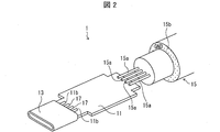
- FIG. 2 is a schematic view showing the arrangement of terminals provided on the paddle card 11 provided in the plug-side connector 1 and the connection state between the plug-side connector 1 and the cable 15.
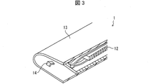
- FIG. 3 is a cross-sectional view showing an outline of the internal structure of the shell portion 13.
- the plug-side connector 1 is electrically connected to the smartphone 600 and the AC adapter 500 by the cable 15 by fitting with the receptable connector 2 provided on the smartphone 600. Then, when the AC adapter 500 and the smartphone 600 are electrically connected, the smartphone 600 can receive power from the AC adapter 500.
- the plug-side connector 1 includes a paddle card 11, a ground terminal 11b, a center plate (metal plate) 12, a shell portion 13, a ground spring 14, and a Vbus terminal 17 (power supply terminal; see FIG. 2). ing. Specifically, the paddle card 11, the center plate 12, the ground spring 14, and the Vbus terminal 17 are disposed inside the shell portion 13.
- the paddle card 11 is, for example, a PWB (Printed Wiring Board), and electronic components, an integrated circuit (IC), and the like (not shown) are mounted on the paddle card 11. Further, at least the ground terminal 11b and the Vbus terminal 17 are formed on the end surface of the paddle card 11 on the shell portion 13 side (see FIG. 2).
- the ground electrode 11a of the paddle card 11 is connected to the ground terminal 11b and is also connected to the center plate 12 via a first capacitor (first protection element) 16a.
- the first capacitor 16a is provided between the center plate 12 and the ground electrode 11a.
- the center plate 12 is a metal plate serving as a ground plane.
- the ground line 15a of the cable 15 is connected to the ground electrode 11a of the paddle card 11 through the ground terminal 11b (see FIG. 2). Further, the outer skin portion (cable outer skin portion) 15b of the cable 15 is not crimped to the shell portion 13, and is connected to the ground electrode 11a of the paddle card 11 via the second capacitor (second protective element) 16b. Connected. In other words, the second capacitor 16b is provided between the outer skin portion 15b of the cable 15 and the ground electrode 11a. The outer skin portion 15b may be crimped to the shell portion 13 as long as it is connected to the ground electrode 11a via the second capacitor 16b.
- the shell portion 13 is a conductive metal case that forms the outline of the plug-side connector 1 and is connected to the ground electrode 11a of the paddle card 11 via a third capacitor (third protection element) 16c.
- the third capacitor 16c is provided between the shell portion 13 and the ground electrode 11a.
- a ground spring 14 is provided on the inner wall surface of the shell portion 13 to make the plug-side connector 1 and the receptacle-side connector 2 fit more reliably.
- the ground spring 14 is also a conductive metal member.
- the plug-side connector according to the present invention is a plug-side connector (not shown) in which the second capacitor 16b is not provided between the outer skin portion 15a of the cable 15 and the ground electrode 11a in the configuration of the plug-side connector 1. Is included as an embodiment.
- the first capacitor 16a, the second capacitor 16b, and the third capacitor 16c are protective elements for preventing a short circuit that occurs between the ground electrode 11a and the Vbus terminal 17. That is, these capacitors 16a to 16c have a characteristic that the impedance becomes low with respect to an alternating current such as a high-frequency current, while the impedance becomes high with respect to a direct current. Therefore, since the capacitors 16a to 16c are in a high impedance state when an overcurrent that is a direct current flows, it is possible to suppress the overcurrent from flowing toward the ground electrode 11a.
- the receptacle-side connector 2 includes a substrate 21, a ground terminal 21 b, a mid plate (metal plate) 22, a shell portion 23, and a Vbus terminal (power supply terminal; see FIG. 8) 25.
- the substrate 21, the ground terminal 21 b, the mid plate 22, and the Vbus terminal 25 are disposed inside the shell portion 23.
- the board 21 for example, an FPC (FlexiblePCPrinted Circuits) which is a flexible circuit board is used, and a ground terminal 21 b connected to the ground terminal 11 b of the plug-side connector 1 and a Vbus terminal of the plug-side connector 1. 17 and a Vbus terminal 25 connected to the terminal 17.
- the ground electrode 21a of the substrate 21 is connected to a mid plate 22 that is a metal plate serving as a ground plane via a first capacitor (first protection element) 24a.
- the first capacitor 24a is provided between the mid plate 22 and the ground electrode 21a.
- the shell portion 23 is a conductive metal case that forms the outline of the receptacle-side connector 2, and is connected to the ground electrode 21a of the substrate 21 through a second capacitor (second protection element) 24b.
- the second capacitor 24b is provided between the shell portion 23 and the ground electrode 21a.
- the shell portion 23 is fitted to the shell portion 13 of the plug-side connector 1 and the outer wall surface of the shell portion 23 is pressed by the ground spring 14.
- the first capacitor 24 a and the second capacitor 24 b are protective elements for preventing a short circuit that occurs between the ground electrode 21 a and the Vbus terminal 25.
- These capacitors 24a and 24b also have a characteristic that the impedance becomes low for an alternating current such as a high-frequency current, while the impedance becomes high for a direct current. Therefore, for example, when foreign matter is mixed in the inside of the shell portion 23 or water droplets are adhered, even if the Vbus terminal 25, the mid plate 22 and the shell portion 23 are in a conductive state, the mid plate 22 Etc., it is possible to effectively prevent the Vbus terminal 25 and the ground electrode 21a from being short-circuited.
- both the plug-side connector 1 and the receptacle-side connector 2 are provided with a short-circuit countermeasure using a capacitor, a short-circuit occurs in the other connector due to a short-circuit in one of the connectors. Such a situation can be prevented.
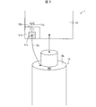
- FIG. 4 is a schematic diagram showing a connection structure of the first capacitor 16 a provided in the plug-side connector 1.
- FIG. 5 is a schematic view showing a connection structure of the second capacitor 16 b provided in the plug-side connector 1.
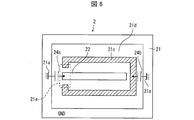
- FIG. 6 is a schematic diagram showing a connection structure of the first capacitor 24a and the second capacitor 24b provided in the receptacle-side connector 2. As shown in FIG.
- a clearance 11d is formed around the region so that the region where the extending portion 12a of the center plate 12 is placed becomes an island 11c. Then, the extending portion 12a and the island 11c are soldered and the island 11c and the ground electrode 11a of the paddle card 11 are connected by the first capacitor 16a.
- a clearance 11d is provided around the region so that the region where the tip of the wiring 15c connected to the outer skin portion 15b of the cable 15 is placed becomes an island 11c. Form. Then, the tip of the wiring 15c and the island 11c are soldered, and the island 11c and the ground electrode 11a of the paddle card 11 are connected by the second capacitor 16b.
- the region of the substrate 21 connected to the opening (not shown) opposite to the opening 23 a in the shell 23 is an island 21 c having a shape corresponding to the shape of the opening.
- a clearance 21d is formed around the region.
- the said opening part in the shell part 23 and the island 21c are connected, and between the said island 21 and the ground electrode 21a of the board
- substrate 21 is connected with the 2nd capacitor
- a clearance 21e is further formed on a part of the island 21c provided on the substrate 21. Then, the first capacitor 24a connects the mid plate 22 and the ground electrode 21a of the substrate 21 through the clearance 21e.
- the plug-side connector 1 and the receptacle-side connector 2 include a Vbus terminal, a ground terminal, and a ground potential portion (corresponding to the center plate 12), and the shell portion has a ground potential.
- the present invention can be applied to all connectors in which the Vbus terminal and the ground electrode of the substrate may be short-circuited through the potential portion.
- the second capacitor 24b is provided between the shell portion 23 and the ground electrode 21a of the substrate 21 to take measures against a short circuit. Therefore, if the receptacle-side connector according to the present invention in which a capacitor as a protection element is provided between the shell portion and the ground electrode is used, the plug-side connector according to the present invention is a shell in the configuration of the plug-side connector 1.
- the embodiment includes a plug-side connector (not shown) in which the third capacitor 16c is not provided between the portion 13 and the ground electrode 11a.
- a capacitor is used as a protective element for short-circuit countermeasures.
- the capacitor has a characteristic that the impedance is reduced with respect to the alternating current while the impedance is increased with respect to the direct current, the capacitor You may use elements other than for a protective element.
- a plug-side connector (not shown) and a receptacle-side connector (not shown) that use a polymer-based PTC thermistor having a positive temperature coefficient as a protective element other than a capacitor are also included in the plug-side connector according to the present invention.
- a receptacle-side connector according to the present invention since the PTC thermistor has a positive temperature characteristic in which the resistance value increases as the temperature rises, the resistance value of the PTC thermistor increases due to heat generation when an overcurrent flows. On the other hand, when an alternating current flows, the temperature does not rise, so the resistance value does not rise. Accordingly, the PTC thermistor functions as a device having a low impedance with respect to an alternating current, while functioning as a device having a high impedance with respect to a direct current, and thus can be used as a protection element.
- the receptacle-side connector 3 according to the present reference embodiment is different from the receptacle-side connector 2 according to the first embodiment in that a midplate (metal plate) 32 is provided instead of the midplate 22.
- the smartphone 600 includes the receptacle-side connector 3.
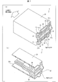
- FIG. 7A is a perspective view showing a schematic configuration of the receptacle-side connector 3.
- FIG. 7B is a cross-sectional view showing an outline of the internal structure of the receptacle-side connector 3.
- the receptacle-side connector 3 includes a mid plate 32 and a shell portion 23.
- the receptacle-side connector 3 includes two terminal groups 37 arranged such that each of the ground terminal 21b, the Vbus terminal 25, and the signal terminal 36 faces the surface 32c of the mid plate 32 (see FIGS. 8 and 9). I have.
- the mid plate 32 is disposed between the two terminal groups 37 inside the shell portion 23.
- the number of the terminal groups 37 may be more than two as long as the mid plate 32 is sandwiched between the two terminal groups 37. Further, the arrangement of the third and subsequent terminal groups 37 inside the shell portion 23 can be arbitrarily designed.
- the mid plate 32 is a metal plate serving as a ground plane, similarly to the mid plate 22 according to the first embodiment.
- the mid plate 32 has an insulating resin portion (insulating member) other than the end surface on the terminal contact side so that the surface 32c and the end surface on the opening 23a side of the shell portion 23 in the mid plate 32 are not exposed. 38).
- FIG. 8 is a schematic diagram showing the shape of the mid plate 32 and the positional relationship between the mid plate 32 and the terminal group 37.
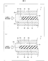
- FIG. 9A shows the configuration of the main part when the receptacle-side connector 3 is viewed in a cut direction defined by the direction in which the Vbus terminal 25 extends and the direction perpendicular to the surface 32c of the midplate 32. It is sectional drawing.
- FIG. 9A shows the configuration of the main part when the receptacle-side connector 3 is viewed in a cut direction defined by the direction in which the Vbus terminal 25 extends and the direction perpendicular to the surface 32c of the midplate 32. It is sectional drawing.
- 9B shows the configuration of the main part when the receptacle-side connector 3 is viewed in a cut direction defined by the direction in which the signal terminal 36 extends and the direction perpendicular to the surface 32c of the mid plate 32. It is sectional drawing.
- the mid plate 32 has an end surface portion 32 a (end surface on the opening side of the shell portion of the metal plate) corresponding to the arrangement position of the Vbus terminal 25 on the end surface on the opening 23 a side of the mid plate 32.
- the shell portion 23 has a shape recessed to the opposite side of the opening portion 23a.
- the mid plate 32 has a mid view in a cut view defined by a direction in which the Vbus terminal 25 extends and a direction perpendicular to the surface 32 c of the mid plate 32.
- the end surface (end surface portion 32 a) on the opening 23 a side of the shell portion 23 of the plate 32 has a shape that is recessed toward the opposite side of the opening 23 a of the shell portion 23.
- the thickness of the resin portion 38 on the opening 23a side of the shell portion 23 covering the end surface portion 32a of the mid plate 32 is such that the end surface portions other than the end surface portion 32a in the mid plate 32 (the ground terminal 21b and the signal terminal 36).
- the end portion corresponding to the arrangement position of the shell portion 23 has a shape larger than the thickness of the resin portion 38 on the opening 23a side of the shell portion 23.
- the mid plate 32 By forming the mid plate 32 in such a shape, for example, even when the plug-side connector 1 is repeatedly inserted and removed, even if the tip of the resin portion 38 on the opening 23a side of the shell portion 23 is slightly scraped and retracted, the mid plate The end face portion 32 a of 32 is present in the resin and is not exposed from the resin portion 38. Therefore, even if foreign matter is mixed in the inside of the shell portion 23 or water droplets adhere to the inside of the shell portion 23 in a state where the tip portion of the shell portion 23 on the opening 23a side is exposed, It is possible to prevent the Vbus terminal 25 from becoming conductive.
- the mid plate 32 is located at the position where the signal terminal 36 is disposed at the end surface on the opening 23 a side of the mid plate 32 rather than the end surface portion 32 a corresponding to the position where the Vbus terminal 25 is disposed.
- the corresponding end surface portion 32b (the end surface on the opening side of the shell portion of the metal plate) has a shape arranged on the opening 23a side.
- the mid plate 32 is a mid plate in a cut view defined by a direction in which the signal terminal 36 extends and a direction perpendicular to the surface 32 c of the mid plate 32.
- the end surface portion 32b of 32 is closer to the opening 23a than the end surface portion 32a of the mid plate 32 in a cut view defined by the direction in which the Vbus terminal 25 extends and the direction perpendicular to the surface 32c of the mid plate 32. It becomes the shape arranged in.
- the mid plate 32 By making the mid plate 32 into such a shape, for example, impedance matching in high-speed transmission can be effectively performed and unnecessary radiation can be suppressed. In addition, when noise comes from the outside toward a signal line (not shown), the mid plate 32 can effectively cut the noise. Therefore, it is possible to reduce the influence of unnecessary radiation and external noise while preventing a short circuit between the Vbus terminal 25 and the ground electrode 21a.
- the purpose of designing the mid plate 32 in the shape as described above is mainly to prevent the mid plate 32 and the Vbus terminal 25 from becoming conductive.
- This object is realized by designing the shape of the mid plate 32 so that the front end surface 25a of the Vbus terminal 25 is arranged closer to the opening 23a than the end surface portion 32a of the mid plate 32 is. Therefore, it is not always necessary to design the shape of the mid plate 32 so that the end surface portion 32b is disposed closer to the opening 23a than the end surface portion 32a of the mid plate 32 is.
- the configuration of the receptacle-side connector 3 according to the present embodiment includes a ground potential portion (corresponding to the mid plate 32) covered with a Vbus terminal and an insulating member, and the ground potential portion is exposed.
- the present invention can be applied to all connectors in which the Vbus terminal and the ground electrode of the substrate may be short-circuited through the ground potential portion.
- FIGS. 10A and 10B are cross-sectional views showing an outline of the internal structure of the receptacle-side connector according to another reference embodiment of the receptacle-side connector according to the reference embodiment.
- the receptacle-side connector according to the reference embodiment is in a direction perpendicular to the surface 32 c of the mid plate 32 at the end portion 48 a of the resin portion 48 on the opening 23 a side of the shell portion 23.
- the receptacle-side connector 4 in which the thickness of the portion covering the surface 32c of the mid plate 32 in the resin portion 48 is thicker than the thickness in the perpendicular direction is included as another reference form.
- the resin part 48 is formed of an insulating resin, like the resin part 38.
- the smartphone 600 includes the receptacle-side connector 4.
- the receptacle-side connector is provided with, for example, an insulating DLC (Diamond-Like) at an end portion 58a on the opening portion 23a side of the shell portion 23 in the resin portion 58.
- the receptacle-side connector 5 provided with a wear-resistant coating 58b such as a carbon coating is included as another reference form.
- the resin portion 58 is also made of an insulating resin.
- the smartphone 600 includes the receptacle-side connector 5.
- the shell in the mid plate 32 can be obtained even if the receptacle-side connector 5 and the plug-side connector fitted to the receptacle-side connector 5 are repeatedly inserted and removed.
- the tip of the portion 23 on the opening 23a side is not exposed. Therefore, it is possible to more reliably prevent the mid plate 32 and the Vbus terminal 25 from becoming conductive.
- an abrasion resistant coating 58b may be applied to the end 48a of the resin portion 48.
- the plug-side connector (1) is engaged with the receptacle-side connector (2, 3, 4, 5) provided in the electronic device (smart phone 600), thereby the electronic device and the external device.
- a plug-side connector for electrically connecting (AC adapter 500) with a cable (15), comprising a conductive shell portion (13) that forms an outer shell of the plug-side connector, and the shell portion are provided with at least a power supply terminal (Vbus terminal 17) and a metal plate (center plate 12) serving as a ground plane, and an alternating current is provided between the metal plate and the ground electrode (11a).
- the first protection element (the first capacitor 1) has a characteristic that the impedance is low with respect to DC, while the impedance is high with respect to DC current. a) is provided, and between the outer skin portion (15b) of the cable and the ground electrode, the impedance is low for an alternating current, while the impedance is high for a direct current. A second protection element (second capacitor 16b) is provided.
- the plug-side connector has the first protective element provided between the metal plate and the ground electrode, and the second protective element provided between the outer skin portion of the cable and the ground electrode. Yes.
- the first protection element and the second protection element have a characteristic that the impedance is reduced with respect to an alternating current, while the impedance is increased with respect to a direct current.
- a direct current is in a high impedance state between the metal plate and the ground electrode and between the outer sheath of the cable and the ground electrode. Therefore, for example, when foreign matter is mixed in the inside of the shell part or water droplets adhere to it, even if the power supply terminal and the metal plate and the outer skin part of the cable become conductive, the metal plate etc. Thus, it is possible to effectively prevent a short circuit between the power supply terminal and the ground electrode.
- the first protection element and the second protection element are capacitors.
- a capacitor has a characteristic that an impedance increases with respect to a direct current while an impedance decreases with respect to a high frequency.
- the first protection element and the second protection element are capacitors, a direct current is generated between the metal plate and the ground electrode and between the outer sheath of the cable and the ground electrode. High-frequency noise components and the like can be released to the ground electrode while creating a high impedance state.
- a plug-side connector according to aspect 3 of the present invention is a plug-side connector for electrically connecting the electronic device and an external device by a cable by fitting with a receptacle-side connector provided in the electronic device.
- a conductive shell portion that forms an outer shell of the plug-side connector is provided, and at least a power supply terminal and a metal plate serving as a ground plane are disposed inside the shell portion, and the metal plate And a ground electrode, a first protection element having a characteristic that an impedance is reduced with respect to an alternating current while an impedance is increased with respect to a direct current is provided, and the shell portion and the ground electrode are provided. In between, it has the characteristic that the impedance is low for alternating current, while the impedance is high for direct current
- the third protection device (third capacitor 16c) are provided.
- the first protection element is provided between the metal plate and the ground electrode
- the third protection element is provided between the shell portion and the ground electrode. Since the third protective element also has a characteristic that the impedance is reduced with respect to the alternating current, while the impedance is increased with respect to the direct current, not only between the metal plate and the ground electrode but also the shell portion and the ground. Even between the electrodes, a high impedance state is obtained with respect to the direct current.
- the first protection element and the third protection element are preferably capacitors.
- the first protection element and the third protection element are capacitors, a high impedance state with respect to a direct current is created between the metal plate and the ground electrode and between the shell portion and the ground electrode. , High-frequency noise components and the like can be removed to the ground electrode.
- a receptacle-side connector (2) according to aspect 5 of the present invention is provided in an electronic device and is fitted with a plug-side connector for electrically connecting the electronic device and an external device via a cable.
- a receptacle-side connector that electrically connects the electronic device and the external device and includes a conductive shell portion (23) that forms an outline of the receptacle-side connector; Includes at least a power supply terminal (Vbus terminal 25) and a metal plate (mid plate 22) to be a ground plane. Between the metal plate and the ground electrode (21b), an AC current is The first protection element (the first capacitor) has a characteristic that the impedance is low while the impedance is high with respect to a direct current. 4a) is provided between the shell portion and the ground electrode, and a second protective element having a characteristic that the impedance is reduced with respect to an alternating current while the impedance is increased with respect to a direct current.
- a second capacitor 24b) is provided.
- the first protective element is provided between the metal plate and the ground electrode, and the second protective element is provided between the shell portion and the ground electrode.
- the first protection element and the second protection element have a characteristic that the impedance is reduced with respect to an alternating current, while the impedance is increased with respect to a direct current.
- a direct current is in a high impedance state between the metal plate and the ground electrode and between the shell portion and the ground electrode. Therefore, for example, when foreign matter is mixed in the inside of the shell part or water droplets are attached, even if the power supply terminal and the metal plate and the shell part become conductive, the power It is possible to effectively prevent a short circuit between the terminal and the ground electrode.
- the first protection element and the second protection element are preferably capacitors.
- the electronic device according to aspect 7 of the present invention preferably includes the receptacle-side connector according to aspect 5 or 6.
- the receptacle-side connector (3, 4, 5) according to aspect 1 of the reference form is provided in the electronic device (smart phone 600), and the electronic device and the external device (AC adapter 500) via the cable (15).
- a terminal group (37) including a ground terminal (21b) and a signal terminal (36), and a metal plate (midplate 32) serving as a ground plane and a conductive shell forming an outline of the receptacle-side connector
- the receptacle-side connector according to Aspect 2 of the reference form is provided in an electronic device, and is fitted with a plug-side connector for electrically connecting the electronic device and an external device via a cable.
- a receptacle-side connector for electrically connecting the electronic device and the external device comprising at least a terminal group including a power supply terminal, a ground terminal and a signal terminal, a metal plate serving as a ground plane, and the receptacle-side connector
- a conductive shell portion that forms an outer shell of the metal plate, and in a cut view defined by a direction in which the power supply terminal extends and a direction perpendicular to the surface (32c) of the metal plate,
- the end surface (end surface portion 32a) on the opening side of the shell portion has a shape that is recessed to the opposite side of the opening portion of the shell portion.
- a receptacle-side connector according to Aspect 3 of the reference embodiment is the receptacle-side connector according to Aspect 1 or 2, in a cut view defined by a direction in which the signal terminal extends and a direction perpendicular to the surface of the metal plate.
- the shell portion of the metal plate in a cut view in which an end surface (end surface portion 32b) on the opening side of the shell portion is defined by a direction in which the power supply terminal extends and a direction perpendicular to the surface of the metal plate. It is preferable to arrange
- the surface of the metal plate and the end surface on the opening side of the shell portion are insulating members (resin portions 48).
- the thickness of the end portion (48a) on the opening side of the shell portion in the insulating member in the direction perpendicular to the surface of the metal plate covers the surface of the metal plate in the insulating member. It is preferable that the thickness of the portion is larger than the thickness in the direction perpendicular to the surface of the metal plate.
- the end surface on the opening side of the surface and the shell part of the metal plate is an insulating member (resin part 58). ), And an end portion (58a) on the opening side of the shell portion of the insulating member is preferably provided with a wear-resistant coating (58b).
- the insulating member is less likely to be scraped even if the plug-side connector that fits into the receptacle-side connector and the receptacle-side connector according to the reference form is repeatedly inserted and removed. The tip is not exposed. Therefore, since it is possible to more reliably prevent the metal plate and the power supply terminal from being in a conductive state, it is possible to more effectively prevent the power supply terminal and the ground electrode from being short-circuited via the metal plate. .
- the electronic device includes the receptacle-side connector according to any one of the first to fifth aspects.
Landscapes
- Engineering & Computer Science (AREA)
- Theoretical Computer Science (AREA)
- Physics & Mathematics (AREA)
- General Engineering & Computer Science (AREA)
- General Physics & Mathematics (AREA)
- Human Computer Interaction (AREA)
- Power Engineering (AREA)
- Microelectronics & Electronic Packaging (AREA)
- Details Of Connecting Devices For Male And Female Coupling (AREA)
- Connector Housings Or Holding Contact Members (AREA)
Abstract
電源端子とグランド電極とが短絡することを効果的に防止する。プラグ側コネクタ(1)は、シェル部(23)の内部において、金属板(センタープレート12)とグランド電極(11a)との間に第1保護素子(第1のコンデンサ16a)が設けられており、ケーブル(15)の外皮部(15b)とグランド電極(11a)との間に第2保護素子(第2のコンデンサ16b)が設けられている。
Description
本発明は、電子機器と外部装置との電気的接続に用いられるプラグ側コネクタ、レセプタクル側コネクタおよび当該レセプタクル側コネクタを備えた電子機器に関する。
従来から、スマートフォン等の電子機器にAC(Alternating Current)アダプタ等の外部の周辺機器を接続するための規格として、USB(Universal Serial Bus)規格が広く用いられている。このUSB規格を用いたUSBインターフェイスにおいて、不意の電源ショート等による過電流からのデバイス保護については、通常、ホスト側に過電流保護機構を実装するという対策が講じられている。
しかし、市場には、過電流保護機構を実装していないUSBホストおよび配線ミスがあるUSBケーブルが存在する。したがって、このようなUSBホストとUSBケーブルとを使用して過電流が流れた場合に、そのことをユーザに通知する技術の研究開発が進められている。
例えば、特許文献1には、信号線や電力線に過電流防止手段、および過電流状態検出手段及び過電流状態通知手段を備えたUSBデバイス装置が開示されている。このUSBデバイス装置は、配線ミスのあるUSBケーブルを用いた場合等であっても、過電流状態検出手段及び過電流状態通知手段によって、異常な接続状態であることをユーザに通知することが可能となっている。
しかしながら、特許文献1に開示された技術は、USBケーブルを介してUSBホスト装置からUSBデバイス装置に電力が供給された場合に、当該USBデバイス装置に設けられたデバイス側コネクタで生じた短絡を検出・通知するものである。したがって、ユーザが短絡に気付いて対処する前に過電流が回路に流れてしまい、USBデバイス装置に不具合等が生じる可能性があった。
また、特許文献1のUSBデバイス装置には、過電流防止手段としてPTC(PositiveTemperature Coefficient)ヒューズが設けられているものの、このヒューズは、デバイス側コネクタに流れる過電流をLED等が接続されている経路に流す役割を果たすものであり、デバイス側コネクタに過電流が流れること自体を防止するものではない。したがって、USBホスト装置のホスト側コネクタで短絡が生じると、当該ホスト側コネクタのグランド電極とデバイス側コネクタのグランド電極とが繋がっていることから、USBケーブルを介してデバイス側コネクタのグランド電極に電源電圧が印加され、結局はデバイス側コネクタでも短絡が生じてしまうという問題点もあった。
本発明は、前記の各問題点に鑑みてなされたものであり、その目的は、電源端子とグランド電極とが短絡することを効果的に防止することができるプラグ側コネクタおよびレセプタクル側コネクタを実現することにある。
上記の課題を解決するために、本発明の一態様に係るプラグ側コネクタは、電子機器に設けられたレセプタブル側コネクタと嵌合することにより、上記電子機器と外部装置とをケーブルにより電気的に接続するためのプラグ側コネクタであって、上記プラグ側コネクタの外郭を形成する導電性のシェル部を備えるとともに、上記シェル部の内部には、少なくとも電源端子と、グランドプレーンとなる金属板と、が配置されており、上記金属板とグランド電極との間に、交流電流に対してはインピーダンスが低くなる一方、直流電流に対してはインピーダンスが高くなる特性を有する第1保護素子が設けられており、上記ケーブルの外皮部と上記グランド電極との間に、交流電流に対してはインピーダンスが低くなる一方、直流電流に対してはインピーダンスが高くなる特性を有する第2保護素子が設けられている。
また、上記の課題を解決するために、本発明の一態様に係るプラグ側コネクタは、電子機器に設けられたレセプタブル側コネクタと嵌合することにより、上記電子機器と外部装置とをケーブルにより電気的に接続するためのプラグ側コネクタであって、上記プラグ側コネクタの外郭を形成する導電性のシェル部を備えるとともに、上記シェル部の内部には、少なくとも電源端子と、グランドプレーンとなる金属板と、が配置されており、上記金属板とグランド電極との間に、交流電流に対してはインピーダンスが低くなる一方、直流電流に対してはインピーダンスが高くなる特性を有する第1保護素子が設けられており、上記シェル部と上記グランド電極との間に、交流電流に対してはインピーダンスが低くなる一方、直流電流に対してはインピーダンスが高くなる特性を有する第3保護素子が設けられている。
また、上記の課題を解決するために、本発明の一態様に係るレセプタクル側コネクタは、電子機器に設けられているとともに、ケーブルを介して上記電子機器と外部装置とを電気的に接続するためのプラグ側コネクタと嵌合することにより、上記電子機器と上記外部装置とを電気的に接続するレセプタクル側コネクタであって、上記レセプタクル側コネクタの外郭を形成する導電性のシェル部を備えるとともに、上記シェル部の内部には、少なくとも電源端子と、グランドプレーンとなる金属板と、が配置されており、上記金属板とグランド電極との間に、交流電流に対してはインピーダンスが低くなる一方、直流電流に対してはインピーダンスが高くなる特性を有する第1保護素子が設けられており、上記シェル部と上記グランド電極との間に、交流電流に対してはインピーダンスが低くなる一方、直流電流に対してはインピーダンスが高くなる特性を有する第2保護素子が設けられている。
本発明の一態様によれば、保護素子を設けることにより、電源端子と金属板等とが導通状態になっても、電源端子とグランド電極とが短絡することを効果的に防止することができる。
〔実施形態1〕
以下、本発明の実施の形態について、図1~図6を参照しながら、詳細に説明する。なお、本実施形態以下の各実施形態および各参考形態においては、本発明および参考形態に係るプラグ側コネクタは、ケーブル15を介してACアダプタ(外部装置)500と電気的に接続している場合について説明する(図1参照)。また、本発明および参考形態に係るレセプタクル側コネクタは、スマートフォン(電子機器)600に設けられている場合について説明する(図1参照)。
以下、本発明の実施の形態について、図1~図6を参照しながら、詳細に説明する。なお、本実施形態以下の各実施形態および各参考形態においては、本発明および参考形態に係るプラグ側コネクタは、ケーブル15を介してACアダプタ(外部装置)500と電気的に接続している場合について説明する(図1参照)。また、本発明および参考形態に係るレセプタクル側コネクタは、スマートフォン(電子機器)600に設けられている場合について説明する(図1参照)。
ただし、本発明および参考形態に係るプラグ側コネクタと電気的に接続している外部装置はACアダプタ500に限られず、例えば、PC(Personal Computer)、携帯型のバッテリー等であってもよい。また、本発明および参考形態に係るレセプタクル側コネクタが設けられている電子機器はスマートフォン600に限られず、例えば、携帯電話機、タブレット端末、携帯型ゲーム機等であってもよい。さらには、本発明および参考形態に係るプラグ側コネクタ、レセプタクル側コネクタは、HDMI(登録商標、High Definition Multimedia Interface;高精細度マルチメディアインターフェイス)にも適用することができる。
<プラグ側コネクタおよびレセプタクル側コネクタの構成>
まず、図1~図3を参照して、プラグ側コネクタ1およびレセプタクル側コネクタ2の主要な構成について説明する。図1は、プラグ側コネクタ1およびレセプタクル側コネクタ2の主要な構成を示すブロック図である。図2は、プラグ側コネクタ1が備えるパドルカード11に設けられた各端子の配置、およびプラグ側コネクタ1とケーブル15との接続状態を示す概略図である。図3は、シェル部13の内部構造の概略を示す断面図である。
まず、図1~図3を参照して、プラグ側コネクタ1およびレセプタクル側コネクタ2の主要な構成について説明する。図1は、プラグ側コネクタ1およびレセプタクル側コネクタ2の主要な構成を示すブロック図である。図2は、プラグ側コネクタ1が備えるパドルカード11に設けられた各端子の配置、およびプラグ側コネクタ1とケーブル15との接続状態を示す概略図である。図3は、シェル部13の内部構造の概略を示す断面図である。
プラグ側コネクタ1は、スマートフォン600に設けられたレセプタブル側コネクタ2と嵌合することによって、スマートフォン600とACアダプタ500とをケーブル15により電気的に接続する。そして、ACアダプタ500とスマートフォン600とが電気的に接続することにより、スマートフォン600は、ACアダプタ500から電力の供給を受けることが可能となる。
図1に示すように、プラグ側コネクタ1は、パドルカード11、グランド端子11b、センタープレート(金属板)12、シェル部13、グランドスプリング14およびVbus端子17(電源端子;図2参照)を備えている。具体的には、シェル部13の内部に、パドルカード11、センタープレート12、グランドスプリング14およびVbus端子17が配置されている。
パドルカード11は、例えばPWB(Printed Wiring Board;プリント配線板)であり、当該パドルカード11上には電子部品および集積回路(IC)等(図示せず)が実装されている。また、パドルカード11の表面におけるシェル部13側の端面には、少なくともグランド端子11bおよびVbus端子17が形成されている(図2参照)。パドルカード11のグランド電極11aは、グランド端子11bと接続しているとともに、第1のコンデンサ(第1保護素子)16aを介してセンタープレート12とも接続している。換言すれば、センタープレート12とグランド電極11aとの間に第1のコンデンサ16aが設けられた構成となっている。ここで、センタープレート12は、グランドプレーンとなる金属板である。
ケーブル15のグランド線15aは、グランド端子11bを介してパドルカード11のグランド電極11aと接続している(図2参照)。また、ケーブル15の外皮部(ケーブルの外皮部)15bは、シェル部13に対して加締められることなく、第2のコンデンサ(第2保護素子)16bを介してパドルカード11のグランド電極11aと接続している。換言すれば、ケーブル15の外皮部15bとグランド電極11aとの間に第2のコンデンサ16bが設けられた構成となっている。なお、上記外皮部15bは、第2のコンデンサ16bを介してグランド電極11aと接続されていれば、シェル部13に対して加締められていてもよい。
シェル部13は、プラグ側コネクタ1の外郭を形成する導電性の金属ケースであり、第3のコンデンサ(第3保護素子)16cを介してパドルカード11のグランド電極11aと接続している。換言すれば、シェル部13とグランド電極11aとの間に第3のコンデンサ16cが設けられた構成となっている。
また、図3に示すように、シェル部13の内壁面には、プラグ側コネクタ1とレセプタクル側コネクタ2との嵌合をより確実にするためのグランドスプリング14が設けられている。グランドスプリング14も、導電性の金属部材である。
また、上記外皮部15bは、シェル部13が第3のコンデンサ16cを介してグランド電極11aと接続されていれば、第2のコンデンサ16bを介してグランド電極11aに接続せずにシェル部13に対して加締めることで、シェル部13を介してグランド電極11aに接続されていてもよい。換言すれば、本発明に係るプラグ側コネクタは、プラグ側コネクタ1の構成においてケーブル15の外皮部15aとグランド電極11aとの間に第2のコンデンサ16bを設けないプラグ側コネクタ(図示せず)を実施形態として含む。
第1のコンデンサ16a、第2のコンデンサ16bおよび第3のコンデンサ16cは、グランド電極11aとVbus端子17との間で生じる短絡を防止するための保護素子である。すなわち、これらのコンデンサ16a~16cは、高周波電流等の交流電流に対してはインピーダンスが低くなる一方、直流電流に対してはインピーダンスが高くなる特性を有する。したがって、これらのコンデンサに16a~16cは、直流電流である過電流が流れる場合には高インピーダンス状態になることから、グランド電極11aに向けて過電流が流れることを抑制することができる。
それゆえ、例えば、シェル部13の内部に異物が混入したり水滴が付着したりした場合に、Vbus端子17と、センタープレート12およびケーブル15の外皮部15bとが導通状態になっても、当該センタープレート12等を介してVbus端子17とグランド電極11aとが短絡することを効果的に防止することができる。また、Vbus端子17とシェル部13とが導通状態になっても、当該シェル部13を介してVbus端子17とグランド電極11aとが短絡することを効果的に防止することができる。
次に、図1に示すように、レセプタクル側コネクタ2は、基板21、グランド端子21b、ミッドプレート(金属板)22、シェル部23およびVbus端子(電源端子;図8参照)25を備えている。具体的には、シェル部23の内部に、基板21、グランド端子21b、ミッドプレート22およびVbus端子25が配置されている。
基板21としては、例えば、柔軟性のある回路基板であるFPC(Flexible Printed Circuits)が用いられており、プラグ側コネクタ1のグランド端子11bと接続するグランド端子21bと、プラグ側コネクタ1のVbus端子17と接続するVbus端子25と、が設けられている。また、基板21のグランド電極21aは、第1のコンデンサ(第1保護素子)24aを介して、グランドプレーンとなる金属板であるミッドプレート22と接続している。換言すれば、ミッドプレート22とグランド電極21aとの間に第1のコンデンサ24aが設けられた構成となっている。
シェル部23は、レセプタクル側コネクタ2の外郭を形成する導電性の金属ケースであり、第2のコンデンサ(第2保護素子)24bを介して基板21のグランド電極21aと接続している。換言すれば、シェル部23とグランド電極21aとの間に第2のコンデンサ24bが設けられた構成となっている。シェル部23は、プラグ側コネクタ1のシェル部13と嵌合するとともに、グランドスプリング14によってシェル部23の外壁面が押圧される。
第1のコンデンサ24aおよび第2のコンデンサ24bは、グランド電極21aとVbus端子25との間で生じる短絡を防止するための保護素子である。これらのコンデンサ24aおよび24bも、高周波電流等の交流電流に対してはインピーダンスが低くなる一方、直流電流に対してはインピーダンスが高くなる特性を有する。それゆえ、例えば、シェル部23の内部に異物が混入したり水滴が付着したりした場合に、Vbus端子25と、ミッドプレート22およびシェル部23とが導通状態になっても、当該ミッドプレート22等を介してVbus端子25とグランド電極21aとが短絡することを効果的に防止することができる。
また、上述のように、プラグ側コネクタ1、レセプタクル側コネクタ2のいずれにおいてもコンデンサを用いた短絡対策が講じられていることから、いずれか一方のコネクタの短絡によって他方のコネクタにも短絡が生じるといった事態を防止することができる。
<コンデンサの接続構造>
次に、図4~図6を参照して、プラグ側コネクタ1およびレセプタクル側コネクタ2のそれぞれに設けられた各コンデンサの接続構造について説明する。図4は、プラグ側コネクタ1に設けられた第1のコンデンサ16aの接続構造を示す概略図である。図5は、プラグ側コネクタ1に設けられた第2のコンデンサ16bの接続構造を示す概略図である。図6は、レセプタクル側コネクタ2に設けられた、第1のコンデンサ24aおよび第2のコンデンサ24bの接続構造を示す概略図である。
次に、図4~図6を参照して、プラグ側コネクタ1およびレセプタクル側コネクタ2のそれぞれに設けられた各コンデンサの接続構造について説明する。図4は、プラグ側コネクタ1に設けられた第1のコンデンサ16aの接続構造を示す概略図である。図5は、プラグ側コネクタ1に設けられた第2のコンデンサ16bの接続構造を示す概略図である。図6は、レセプタクル側コネクタ2に設けられた、第1のコンデンサ24aおよび第2のコンデンサ24bの接続構造を示す概略図である。
図4に示すように、パドルカード11における、センタープレート12の延伸部12aが載置される領域が島11cになるように、当該領域周辺にクリアランス11dを形成する。そして、延伸部12aと島11cとをはんだ付けするとともに、当該島11cとパドルカード11のグランド電極11aとの間を第1のコンデンサ16aにて接続する。
また、図5に示すように、パドルカード11における、ケーブル15の外皮部15bと接続している配線15cの先端部が載置される領域が島11cになるように、当該領域周辺にクリアランス11dを形成する。そして、配線15cの先端部と島11cとをはんだ付けするとともに、当該島11cとパドルカード11のグランド電極11aとの間を第2のコンデンサ16bにて接続する。
また、図6に示すように、基板21における、シェル部23における開口部23aと反対側の開口部(図示せず)と接続する領域が、当該開口部の形状と対応する形状の島21cになるように、当該領域周辺にクリアランス21dを形成する。そして、シェル部23における上記開口部と島21cとを接続するとともに、当該島21と基板21のグランド電極21aとの間を第2のコンデンサ24bにて接続する。
また、基板21に設けた島21cの一部に、さらにクリアランス21eを形成する。そして、このクリアランス21eを介して、ミッドプレート22と基板21のグランド電極21aとの間を第1のコンデンサ24aにて接続する。
なお、本実施形態に係るプラグ側コネクタ1およびレセプタクル側コネクタ2の構成は、Vbus端子、グランド端子およびグランド電位部(センタープレート12等に対応)を備え、かつシェル部がグランド電位であり、グランド電位部を介してVbus端子と基板のグランド電極とが短絡する可能性のあるコネクタ全般に適用することができる。
〔実施形態2〕
本発明の他の実施形態について、以下に説明する。なお、説明の便宜上、前記実施形態にて説明した部材と同じ機能を有する部材については、同じ符号を付記し、その説明を省略する。
本発明の他の実施形態について、以下に説明する。なお、説明の便宜上、前記実施形態にて説明した部材と同じ機能を有する部材については、同じ符号を付記し、その説明を省略する。
上述のように、実施形態1に係るレセプタクル側コネクタ2においては、シェル部23と基板21のグランド電極21aとの間に第2のコンデンサ24bを設けて短絡対策が施されている。したがって、シェル部とグランド電極との間に保護素子としてのコンデンサが設けられた本発明に係るレセプタクル側コネクタを用いるのであれば、本発明に係るプラグ側コネクタは、プラグ側コネクタ1の構成においてシェル部13とグランド電極11aとの間に第3のコンデンサ16cを設けないプラグ側コネクタ(図示せず)を実施形態として含む。
〔実施形態3〕
本発明の他の実施形態について、以下に説明する。なお、説明の便宜上、前記実施形態にて説明した部材と同じ機能を有する部材については、同じ符号を付記し、その説明を省略する。
本発明の他の実施形態について、以下に説明する。なお、説明の便宜上、前記実施形態にて説明した部材と同じ機能を有する部材については、同じ符号を付記し、その説明を省略する。
実施形態1および2では、短絡対策用の保護素子としてコンデンサを用いているものの、交流電流に対してインピーダンスが低くなる一方、直流電流に対してインピーダンスが高くなる特性を有するものであれば、コンデンサ以外の素子を保護素子に用いてもよい。
例えば、コンデンサ以外の保護素子として、正の温度係数を有するポリマ系のPTCサーミスタを用いたプラグ側コネクタ(図示せず)およびレセプタクル側コネクタ(図示せず)も、それぞれ本発明に係るプラグ側コネクタおよび本発明に係るレセプタクル側コネクタに含まれる。すなわち、PTCサーミスタは、温度が上がると抵抗値が上昇する正温度特性を有していることから、過電流が流れた時の発熱によってPTCサーミスタの抵抗値は上昇する。一方、交流電流が流れた場合には温度上昇しないことから抵抗値も上昇しない。したがって、PTCサーミスタは、交流電流に対してはインピーダンスが低いデバイスとして機能する一方、直流電流に対してはインピーダンスが高いデバイスとして機能することから、保護素子として用いることができる。
〔参考形態1〕
電源端子とグランド電極との間で生じる短絡防止は、上述の各実施形態にて説明したプラグ側コネクタの構成およびレセプタクル側コネクタの構成によって実現されるものの、これらの構成に限定されるものではない。
電源端子とグランド電極との間で生じる短絡防止は、上述の各実施形態にて説明したプラグ側コネクタの構成およびレセプタクル側コネクタの構成によって実現されるものの、これらの構成に限定されるものではない。
以下、電源端子とグランド電極との間で生じる短絡防止を実現するための参考形態について、図7~図9を参照しながら、詳細に説明する。なお、説明の便宜上、前記各実施形態にて説明した部材と同じ機能を有する部材については、同じ符号を付記し、その説明を省略する。
本参考形態に係るレセプタクル側コネクタ3は、ミッドプレート22に代えてミッドプレート(金属板)32を備えている点で、実施形態1に係るレセプタクル側コネクタ2と異なる。この場合、スマートフォン600は、レセプタクル側コネクタ3を備えることとなる。
<レセプタクル側コネクタの構成>
まず、図7を参照して、本参考形態に係るレセプタクル側コネクタ3の主要な構成について説明する。図7の(a)は、レセプタクル側コネクタ3の概略構成を示す斜視図である。図7の(b)は、レセプタクル側コネクタ3の内部構造の概略を示す断面図である。
まず、図7を参照して、本参考形態に係るレセプタクル側コネクタ3の主要な構成について説明する。図7の(a)は、レセプタクル側コネクタ3の概略構成を示す斜視図である。図7の(b)は、レセプタクル側コネクタ3の内部構造の概略を示す断面図である。
図7の(a)および(b)に示すように、レセプタクル側コネクタ3は、ミッドプレート32およびシェル部23を備えている。また、レセプタクル側コネクタ3は、グランド端子21b、Vbus端子25および信号端子36のそれぞれがミッドプレート32の表面32c(図8および図9参照)と対向するよう配置された端子群37を、2つ備えている。具体的には、シェル部23の内部において、ミッドプレート32が2つの端子群37によって挟まれるように配置されている。
なお、ミッドプレート32が2つの端子群37によって挟まれる構成になっていれば、端子群37の個数は2つより多くてもよい。また、シェル部23の内部における3つ目以降の端子群37の配置についても、任意に設計することができる。
ミッドプレート32は、実施形態1に係るミッドプレート22と同様に、グランドプレーンとなる金属板である。また、ミッドプレート32は、その表面32c、および当該ミッドプレート32におけるシェル部23の開口部23a側の端面が露出しないように、端子コンタクト側の端面以外の部分が絶縁性の樹脂部(絶縁部材)38によって覆われている。
<ミッドプレートの形状および端子群との位置関係>
次に、図8および図9を参照して、ミッドプレート32の形状および端子群37との位置関係について説明する。図8は、ミッドプレート32の形状および当該ミッドプレート32と端子群37との位置関係を示す概略図である。図9の(a)は、レセプタクル側コネクタ3を、Vbus端子25が延在する方向とミッドプレート32の表面32cに垂直な方向とで規定される切断視した場合における、主要部の構成を示す断面図である。図9の(b)は、レセプタクル側コネクタ3を、信号端子36が延在する方向とミッドプレート32の表面32cに垂直な方向とで規定される切断視した場合における、主要部の構成を示す断面図である。
次に、図8および図9を参照して、ミッドプレート32の形状および端子群37との位置関係について説明する。図8は、ミッドプレート32の形状および当該ミッドプレート32と端子群37との位置関係を示す概略図である。図9の(a)は、レセプタクル側コネクタ3を、Vbus端子25が延在する方向とミッドプレート32の表面32cに垂直な方向とで規定される切断視した場合における、主要部の構成を示す断面図である。図9の(b)は、レセプタクル側コネクタ3を、信号端子36が延在する方向とミッドプレート32の表面32cに垂直な方向とで規定される切断視した場合における、主要部の構成を示す断面図である。
図8に示すように、ミッドプレート32は、当該ミッドプレート32の開口部23a側端面における、Vbus端子25の配置位置に対応する端面部分32a(金属板のシェル部の開口部側の端面)が、シェル部23の開口部23aの反対側へ奥まった形状になっている。
換言すれば、ミッドプレート32は、図9の(a)に示すように、Vbus端子25が延在する方向と当該ミッドプレート32の表面32cに垂直な方向とで規定される切断視において、ミッドプレート32のシェル部23の開口部23a側の端面(端面部分32a)が、シェル部23の開口部23aの反対側へ奥まった形状になっている。また、ミッドプレート32の上記端面部分32aを覆っているシェル部23の開口部23a側の樹脂部38の厚みが、ミッドプレート32における上記端面部分32a以外の端面部分(グランド端子21bおよび信号端子36の配置位置に対応する端面部分)を覆っているシェル部23の開口部23a側の樹脂部38の厚みよりも多い形状になっている。
ミッドプレート32をこのような形状にすることで、例えば、プラグ側コネクタ1の抜き差しを繰り返して樹脂部38におけるシェル部23の開口部23a側の先端部が多少削れて後退しても、ミッドプレート32の端面部分32aは樹脂内に存在しており樹脂部38から露出することが無い。それゆえ、シェル部23の開口部23a側の先端部が露出した状態において、シェル部23の内部に異物が混入したり水滴が付着したりした場合でも、当該異物等を介してミッドプレート32とVbus端子25とが導通状態になるのを防ぐことができる。
またこの時、図8に示すように、ミッドプレート32は、当該ミッドプレート32の開口部23a側端面において、Vbus端子25の配置位置に対応する端面部分32aよりも、信号端子36の配置位置に対応する端面部分32b(金属板のシェル部の開口部側の端面)の方が開口部23a側に配置された形状になっている。
換言すれば、ミッドプレート32は、図9の(b)に示すように、信号端子36が延在する方向とミッドプレート32の表面32cに垂直な方向とで規定される切断視における、ミッドプレート32の上記端面部分32bが、Vbus端子25が延在する方向とミッドプレート32の表面32cに垂直な方向とで規定される切断視における、ミッドプレート32の上記端面部分32aよりも開口部23a側に配置された形状となっている。
ミッドプレート32をこのような形状にすることで、例えば、高速伝送におけるインピーダンスマッチングを効果的に行うとともに不要輻射も抑えることができる。また、外部から信号線(図示せず)に向けてノイズが飛来した場合に、ミッドプレート32によって当該ノイズを効果的にカットすることができる。したがって、Vbus端子25とグランド電極21aとの短絡防止を図りつつ、不要輻射と外部のノイズの影響を低減することができる。
なお、ミッドプレート32を上述のような形状に設計した目的は、主として、ミッドプレート32とVbus端子25とが導通状態になるのを防ぐためである。この目的は、ミッドプレート32の形状を、当該ミッドプレート32の端面部分32aよりもVbus端子25の先端面25aの方が開口部23a側に配置されるように設計することで実現されている。したがって、ミッドプレート32の形状を、当該ミッドプレート32における端面部分32aよりも端面部分32bの方が開口部23a側に配置されるように設計する必要は必ずしもない。
また、本参考形態に係るレセプタクル側コネクタ3の構成は、Vbus端子および絶縁部材で周囲を覆われているグランド電位部(ミッドプレート32に対応)を備え、かつ、グランド電位部が露出することにより、当該グランド電位部を介してVbus端子と基板のグランド電極とが短絡する可能性のあるコネクタ全般に適用することができる。
〔参考形態2〕
参考形態に係るレセプタクル側コネクタのバリエーションとしては、上述したレセプタクル側コネクタ3のみならず、様々なバリエーションが想定される。以下、電源端子とグランド電極との間で生じる短絡防止を実現するための他の参考形態に係るレセプタクル側コネクタについて、図10を参照しながら、詳細に説明する。なお、説明の便宜上、前記各実施形態および参考形態にて説明した部材と同じ機能を有する部材については、同じ符号を付記し、その説明を省略する。図10の(a)および(b)は、参考形態に係るレセプタクル側コネクタの他の参考形態に係るレセプタクル側コネクタの内部構造の概略を示す断面図である。
参考形態に係るレセプタクル側コネクタのバリエーションとしては、上述したレセプタクル側コネクタ3のみならず、様々なバリエーションが想定される。以下、電源端子とグランド電極との間で生じる短絡防止を実現するための他の参考形態に係るレセプタクル側コネクタについて、図10を参照しながら、詳細に説明する。なお、説明の便宜上、前記各実施形態および参考形態にて説明した部材と同じ機能を有する部材については、同じ符号を付記し、その説明を省略する。図10の(a)および(b)は、参考形態に係るレセプタクル側コネクタの他の参考形態に係るレセプタクル側コネクタの内部構造の概略を示す断面図である。
<レセプタクル側コネクタのバリエーション>
まず、参考形態に係るレセプタクル側コネクタは、図10の(a)に示すように、樹脂部48におけるシェル部23の開口部23a側の端部48aの、ミッドプレート32の表面32cに垂直な方向の厚みが、樹脂部48におけるミッドプレート32の表面32cを覆っている部分の、上記垂直な方向の厚みよりも厚くなっているレセプタクル側コネクタ4を他の参考形態として含む。樹脂部48は、樹脂部38と同様に、絶縁性の樹脂で形成されている。この場合、スマートフォン600は、レセプタクル側コネクタ4を備えることとなる。
まず、参考形態に係るレセプタクル側コネクタは、図10の(a)に示すように、樹脂部48におけるシェル部23の開口部23a側の端部48aの、ミッドプレート32の表面32cに垂直な方向の厚みが、樹脂部48におけるミッドプレート32の表面32cを覆っている部分の、上記垂直な方向の厚みよりも厚くなっているレセプタクル側コネクタ4を他の参考形態として含む。樹脂部48は、樹脂部38と同様に、絶縁性の樹脂で形成されている。この場合、スマートフォン600は、レセプタクル側コネクタ4を備えることとなる。
樹脂部48の形状を上述のようにすることによって、端部48a付近が多少削れても、ミッドプレート32におけるシェル部23の開口部23a側の先端部が露出することがなくなる。それゆえ、ミッドプレート32とVbus端子25とが導通状態になるのをより確実に防ぐことができる。
また、参考形態に係るレセプタクル側コネクタは、図10の(b)に示すように、樹脂部58におけるシェル部23の開口部23a側の端部58aに、例えば絶縁性を有するDLC(Diamond-Like Carbon)コーティング等の耐摩耗性のコーティング58bが施されているレセプタクル側コネクタ5を他の参考形態として含む。樹脂部58も、樹脂部38および48と同様に、絶縁性の樹脂で形成されている。この場合、スマートフォン600は、レセプタクル側コネクタ5を備えることとなる。
樹脂部58の端部58aに上述のような処理を施すことによって、レセプタクル側コネクタ5と、当該レセプタクル側コネクタ5と嵌合するプラグ側コネクタとの抜き差しを多少繰り返しても、ミッドプレート32におけるシェル部23の開口部23a側の先端部が露出することはない。それゆえ、ミッドプレート32とVbus端子25とが導通状態になるのをより確実に防ぐことができる。
なお、図示しないものの、樹脂部48の端部48aに耐摩耗性のコーティング58bを施してもよい。このような構成を採用することにより、ミッドプレート32におけるシェル部23の開口部23a側の先端部が露出することを、より確実に低減することができる。
〔まとめ〕
本発明の態様1に係るプラグ側コネクタ(1)は、電子機器(スマートフォン600)に設けられたレセプタブル側コネクタ(2、3、4、5)と嵌合することにより、上記電子機器と外部装置(ACアダプタ500)とをケーブル(15)により電気的に接続するためのプラグ側コネクタであって、上記プラグ側コネクタの外郭を形成する導電性のシェル部(13)を備えるとともに、上記シェル部の内部には、少なくとも電源端子(Vbus端子17)と、グランドプレーンとなる金属板(センタープレート12)と、が配置されており、上記金属板とグランド電極(11a)との間に、交流電流に対してはインピーダンスが低くなる一方、直流電流に対してはインピーダンスが高くなる特性を有する第1保護素子(第1のコンデンサ16a)が設けられており、上記ケーブルの外皮部(15b)と上記グランド電極との間に、交流電流に対してはインピーダンスが低くなる一方、直流電流に対してはインピーダンスが高くなる特性を有する第2保護素子(第2のコンデンサ16b)が設けられている。
本発明の態様1に係るプラグ側コネクタ(1)は、電子機器(スマートフォン600)に設けられたレセプタブル側コネクタ(2、3、4、5)と嵌合することにより、上記電子機器と外部装置(ACアダプタ500)とをケーブル(15)により電気的に接続するためのプラグ側コネクタであって、上記プラグ側コネクタの外郭を形成する導電性のシェル部(13)を備えるとともに、上記シェル部の内部には、少なくとも電源端子(Vbus端子17)と、グランドプレーンとなる金属板(センタープレート12)と、が配置されており、上記金属板とグランド電極(11a)との間に、交流電流に対してはインピーダンスが低くなる一方、直流電流に対してはインピーダンスが高くなる特性を有する第1保護素子(第1のコンデンサ16a)が設けられており、上記ケーブルの外皮部(15b)と上記グランド電極との間に、交流電流に対してはインピーダンスが低くなる一方、直流電流に対してはインピーダンスが高くなる特性を有する第2保護素子(第2のコンデンサ16b)が設けられている。
上記構成によれば、プラグ側コネクタは、金属板とグランド電極との間に第1保護素子が設けられているとともに、ケーブルの外皮部とグランド電極との間に第2保護素子が設けられている。また、第1保護素子および第2保護素子は、交流電流に対してはインピーダンスが低くなる一方、直流電流に対してはインピーダンスが高くなる特性を有する。
したがって、金属板とグランド電極との間およびケ-ブルの外皮部とグランド電極との間は、直流電流については高インピーダンス状態になっている。それゆえ、例えば、シェル部の内部に異物が混入したり水滴が付着したりした場合に、電源端子と、金属板およびケーブルの外皮部とが導通状態になっても、当該金属板等を介して電源端子とグランド電極とが短絡することを効果的に防止することができる。
本発明の態様2に係るプラグ側コネクタは、上記態様1において、上記第1保護素子および上記第2保護素子は、コンデンサであることが好ましい。
一般に、コンデンサは、直流電流に対してはインピーダンスが高くなる一方、高周波に対してはインピーダンスが低くなるという特性がある。その点、上記構成によれば、第1保護素子および第2保護素子はコンデンサであることから、金属板とグランド電極との間およびケ-ブルの外皮部とグランド電極との間において、直流電流に対する高インピーダンス状態をつくりつつ、高周波のノイズ成分等をグランド電極へ抜けさせることができる。
それゆえ、電源端子とグランド電極との短絡防止を図りつつ、外部のノイズ等による影響を受けにくい、かつ高速伝送を可能にするプラグ側コネクタを実現することができる。
本発明の態様3に係るプラグ側コネクタは、電子機器に設けられたレセプタブル側コネクタと嵌合することにより、上記電子機器と外部装置とをケーブルにより電気的に接続するためのプラグ側コネクタであって、上記プラグ側コネクタの外郭を形成する導電性のシェル部を備えるとともに、上記シェル部の内部には、少なくとも電源端子と、グランドプレーンとなる金属板と、が配置されており、上記金属板とグランド電極との間に、交流電流に対してはインピーダンスが低くなる一方、直流電流に対してはインピーダンスが高くなる特性を有する第1保護素子が設けられており、上記シェル部と上記グランド電極との間に、交流電流に対してはインピーダンスが低くなる一方、直流電流に対してはインピーダンスが高くなる特性を有する第3保護素子(第3のコンデンサ16c)が設けられている。
上記構成によれば、プラグ側コネクタは、金属板とグランド電極との間に第1保護素子が設けられているとともに、シェル部とグランド電極との間に第3保護素子が設けられている。第3保護素子も、交流電流に対してはインピーダンスが低くなる一方、直流電流に対してはインピーダンスが高くなる特性を有することから、金属板とグランド電極との間のみならず、シェル部とグランド電極との間においても直流電流に対して高インピーダンス状態となる。
それゆえ、例えば、シェル部の内部に異物が混入したり水滴が付着したりした場合に、電源端子とシェル部とが導通状態になっても、当該シェル部を介して電源端子とグランド電極とが短絡することを効果的に防止することができる。
本発明の態様4に係るプラグ側コネクタは、上記態様3において、上記第1保護素子および上記第3保護素子は、コンデンサであることが好ましい。
上記構成によれば、第1保護素子および第3保護素子はコンデンサであることから、金属板とグランド電極との間およびシェル部とグランド電極との間において、直流電流に対する高インピーダンス状態をつくりつつ、高周波のノイズ成分等をグランド電極へ抜けさせることができる。
本発明の態様5に係るレセプタクル側コネクタ(2)は、電子機器に設けられているとともに、ケーブルを介して上記電子機器と外部装置とを電気的に接続するためのプラグ側コネクタと嵌合することにより、上記電子機器と上記外部装置とを電気的に接続するレセプタクル側コネクタであって、上記レセプタクル側コネクタの外郭を形成する導電性のシェル部(23)を備えるとともに、上記シェル部の内部には、少なくとも電源端子(Vbus端子25)と、グランドプレーンとなる金属板(ミッドプレート22)と、が配置されており、上記金属板とグランド電極(21b)との間に、交流電流に対してはインピーダンスが低くなる一方、直流電流に対してはインピーダンスが高くなる特性を有する第1保護素子(第1のコンデンサ24a)が設けられており、上記シェル部と上記グランド電極との間に、交流電流に対してはインピーダンスが低くなる一方、直流電流に対してはインピーダンスが高くなる特性を有する第2保護素子(第2のコンデンサ24b)が設けられている。
上記構成によれば、レセプタクル側コネクタは、金属板とグランド電極との間に第1保護素子が設けられているとともに、シェル部とグランド電極との間に第2保護素子が設けられている。また、第1保護素子および第2保護素子は、交流電流に対してはインピーダンスが低くなる一方、直流電流に対してはインピーダンスが高くなる特性を有する。
したがって、金属板とグランド電極との間およびシェル部とグランド電極との間では、直流電流については高インピーダンス状態になっている。それゆえ、例えば、シェル部の内部に異物が混入したり水滴が付着したりした場合に、電源端子と、金属板およびシェル部とが導通状態になっても、当該金属板等を介して電源端子とグランド電極とが短絡することを効果的に防止することができる。
本発明の態様6に係るレセプタクル側コネクタは、上記態様5において、上記第1保護素子および上記第2保護素子は、コンデンサであることが好ましい。
上記構成によれば、電源端子とグランド電極との短絡防止を図りつつ、外部のノイズ等による影響を受けにくい、かつ高速伝送を可能にするレセプタクル側コネクタを実現することができる。
本発明の態様7に係る電子機器は、上記態様5または6に係るレセプタクル側コネクタを備えていることが好ましい。
上記構成によれば、電源端子とグランド電極とが短絡することを効果的に防止できるレセプタクル側コネクタを備えた電子機器を実現することができる。
本発明は上述した各実施形態に限定されるものではなく、請求項に示した範囲で種々の変更が可能であり、異なる実施形態にそれぞれ開示された技術的手段を適宜組み合わせて得られる実施形態についても本発明の技術的範囲に含まれる。さらに、各実施形態にそれぞれ開示された技術的手段を組み合わせることにより、新しい技術的特徴を形成することができる。
〔補足事項〕
参考形態の態様1に係るレセプタクル側コネクタ(3、4、5)は、電子機器(スマートフォン600)に設けられているとともに、ケーブル(15)を介して上記電子機器と外部装置(ACアダプタ500)とを電気的に接続するためのプラグ側コネクタ(1)と嵌合することにより、上記電子機器と上記外部装置とを電気的に接続するレセプタクル側コネクタであって、電源端子(Vbus端子25)、グランド端子(21b)および信号端子(36)を含む端子群(37)を少なくとも備えるとともに、グランドプレーンとなる金属板(ミッドプレート32)と、上記レセプタクル側コネクタの外郭を形成する導電性のシェル部(23)と、を備え、上記シェル部の内部において、上記金属板の上記シェル部の開口部(23a)側の端面における、上記電源端子の配置位置に対応する端面(端面部分32a)が、上記シェル部の開口部の反対側へ奥まった形状になっていることを特徴としている。
参考形態の態様1に係るレセプタクル側コネクタ(3、4、5)は、電子機器(スマートフォン600)に設けられているとともに、ケーブル(15)を介して上記電子機器と外部装置(ACアダプタ500)とを電気的に接続するためのプラグ側コネクタ(1)と嵌合することにより、上記電子機器と上記外部装置とを電気的に接続するレセプタクル側コネクタであって、電源端子(Vbus端子25)、グランド端子(21b)および信号端子(36)を含む端子群(37)を少なくとも備えるとともに、グランドプレーンとなる金属板(ミッドプレート32)と、上記レセプタクル側コネクタの外郭を形成する導電性のシェル部(23)と、を備え、上記シェル部の内部において、上記金属板の上記シェル部の開口部(23a)側の端面における、上記電源端子の配置位置に対応する端面(端面部分32a)が、上記シェル部の開口部の反対側へ奥まった形状になっていることを特徴としている。
これにより、例えば、プラグ側コネクタの抜き差しを繰り返して絶縁部材におけるシェル部の開口部側の先端部が多少削れて後退しても、金属板における電源端子の配置位置に対応する端面は絶縁部材内に存在しており絶縁部材から露出することが無い。それゆえ、シェル部の内部に異物が混入したり水滴が付着したりした場合でも、当該異物等を介して金属板と電源端子とが導通状態になるのを防ぐことができる。それゆえ、金属板を介して電源端子とグランド電極とが短絡することを効果的に防止できるレセプタクル側コネクタを実現することができる。
参考形態の態様2に係るレセプタクル側コネクタは、電子機器に設けられているとともに、ケーブルを介して上記電子機器と外部装置とを電気的に接続するためのプラグ側コネクタと嵌合することにより、上記電子機器と上記外部装置とを電気的に接続するレセプタクル側コネクタであって、電源端子、グランド端子および信号端子を含む端子群を少なくとも備えるとともに、グランドプレーンとなる金属板と、上記レセプタクル側コネクタの外郭を形成する導電性のシェル部と、を備え、上記電源端子が延在する方向と上記金属板の表面(32c)に垂直な方向とで規定される切断視において、上記金属板の上記シェル部の開口部側の端面(端面部分32a)が、上記シェル部の開口部の反対側へ奥まった形状になっていることを特徴としている。
これにより、例えば、プラグ側コネクタの抜き差しを繰り返して絶縁部材におけるシェル部の開口部側の先端部が多少削れて後退しても、金属板における電源端子の配置位置に対応する端面が絶縁部材から露出することが無い。それゆえ、シェル部の内部に異物が混入したり水滴が付着したりした場合でも、当該異物等を介して金属板と電源端子とが導通状態になるのを防ぐことができる。
参考形態の態様3に係るレセプタクル側コネクタは、上記態様1または2において、上記信号端子が延在する方向と上記金属板の表面に垂直な方向とで規定される切断視における、上記金属板の上記シェル部の開口部側の端面(端面部分32b)が、上記電源端子が延在する方向と上記金属板の表面に垂直な方向とで規定される切断視における、上記金属板の上記シェル部の開口部側の端面よりも、上記シェル部の開口部側に配置されていることが好ましい。
これにより、例えば、高速伝送におけるインピーダンスマッチングを効果的に行うとともに不要輻射も抑えることができる。また、金属板におけるシェル部の開口部側の先端部が露出した状態において、外部から信号端子と接続している信号線に向けてノイズが飛来した場合に、金属板によって当該ノイズを効果的にカットすることができる。それゆえ、電源端子とグランド電極との短絡防止を図りつつ、不要輻射と外部のノイズの影響を受けにくいレセプタクル側コネクタを実現することができる。
参考形態の態様4に係るレセプタクル側コネクタ(4)は、上記態様1から3のいずれかにおいて、上記金属板における、上記表面および上記シェル部の開口部側の端面は、絶縁部材(樹脂部48)で覆われており、上記絶縁部材における上記シェル部の開口部側の端部(48a)の、上記金属板の表面に垂直な方向の厚みが、上記絶縁部材における上記金属板の表面を覆っている部分の、上記金属板の表面に垂直な方向の厚みよりも厚くなっていることが好ましい。
これにより、絶縁部材におけるシェル部の開口部側の端部付近が多少削れても、金属板におけるシェル部の開口部側の先端部が露出することはない。それゆえ、金属板と電源端子とが導通状態になるのをより確実に防ぐことができることから、金属板を介して電源端子とグランド電極とが短絡することをより効果的に防止することができる。
参考形態の態様5に係るレセプタクル側コネクタ(5)は、上記態様1から4のいずれかにおいて、上記金属板における、上記表面および上記シェル部の開口部側の端面は、絶縁部材(樹脂部58)で覆われており、上記絶縁部材における上記シェル部の開口部側の端部(58a)には、耐摩耗性のコーティング(58b)が施されていることが好ましい。
これにより、参考形態に係るレセプタクル側コネクタと、当該レセプタクル側コネクタと嵌合するプラグ側コネクタとの抜き差しを多少繰り返しても、絶縁部材が削れにくくなるため、金属板におけるシェル部の開口部側の先端部が露出することはない。それゆえ、金属板と電源端子とが導通状態になるのをより確実に防ぐことができることから、金属板を介して電源端子とグランド電極とが短絡することをより効果的に防止することができる。
参考形態の態様6に係る電子機器は、上記態様1から5のいずれかに係るレセプタクル側コネクタを備えていることが好ましい。
これにより、電源端子とグランド電極とが短絡することを効果的に防止できるレセプタクル側コネクタを備えた電子機器を実現することができる。
1 プラグ側コネクタ 2、3、4、5 レセプタクル側コネクタ
11a、21a グランド電極 11b、21b グランド端子
12 センタープレート(金属板) 13、23 シェル部 15 ケーブル
15b 外皮部(ケーブルの外皮部)
16a、24a 第1のコンデンサ(第1保護素子)
16b、24b 第2のコンデンサ(第2保護素子)
16c 第3のコンデンサ(第3保護素子) 17、25 Vbus端子(電源端子)22、32 ミッドプレート(金属板) 23a 開口部(シェル部の開口部)
25a 先端面
32a 端面部分(電源端子の配置位置に対応する端面、金属板のシェル部の開口部側の端面) 32b 端面部分(金属板のシェル部の開口部側の端面)
32c 表面(金属板の表面) 36 信号端子 37 端子群
38、48、58 樹脂部(絶縁部材)
48a、58a 端部(絶縁部材におけるシェル部の開口部側の端部)
58b コーティング(耐摩耗性のコーティング)
500 ACアダプタ(外部装置) 600 スマートフォン(電子機器)
11a、21a グランド電極 11b、21b グランド端子
12 センタープレート(金属板) 13、23 シェル部 15 ケーブル
15b 外皮部(ケーブルの外皮部)
16a、24a 第1のコンデンサ(第1保護素子)
16b、24b 第2のコンデンサ(第2保護素子)
16c 第3のコンデンサ(第3保護素子) 17、25 Vbus端子(電源端子)22、32 ミッドプレート(金属板) 23a 開口部(シェル部の開口部)
25a 先端面
32a 端面部分(電源端子の配置位置に対応する端面、金属板のシェル部の開口部側の端面) 32b 端面部分(金属板のシェル部の開口部側の端面)
32c 表面(金属板の表面) 36 信号端子 37 端子群
38、48、58 樹脂部(絶縁部材)
48a、58a 端部(絶縁部材におけるシェル部の開口部側の端部)
58b コーティング(耐摩耗性のコーティング)
500 ACアダプタ(外部装置) 600 スマートフォン(電子機器)
Claims (7)
- 電子機器に設けられたレセプタブル側コネクタと嵌合することにより、上記電子機器と外部装置とをケーブルにより電気的に接続するためのプラグ側コネクタであって、
上記プラグ側コネクタの外郭を形成する導電性のシェル部を備えるとともに、上記シェル部の内部には、少なくとも電源端子と、グランドプレーンとなる金属板と、が配置されており、
上記金属板とグランド電極との間に、交流電流に対してはインピーダンスが低くなる一方、直流電流に対してはインピーダンスが高くなる特性を有する第1保護素子が設けられており、
上記ケーブルの外皮部と上記グランド電極との間に、交流電流に対してはインピーダンスが低くなる一方、直流電流に対してはインピーダンスが高くなる特性を有する第2保護素子が設けられていることを特徴とするプラグ側コネクタ。 - 上記第1保護素子および上記第2保護素子は、コンデンサであることを特徴とする請求項1に記載のプラグ側コネクタ。
- 電子機器に設けられたレセプタブル側コネクタと嵌合することにより、上記電子機器と外部装置とをケーブルにより電気的に接続するためのプラグ側コネクタであって、
上記プラグ側コネクタの外郭を形成する導電性のシェル部を備えるとともに、上記シェル部の内部には、少なくとも電源端子と、グランドプレーンとなる金属板と、が配置されており、
上記金属板とグランド電極との間に、交流電流に対してはインピーダンスが低くなる一方、直流電流に対してはインピーダンスが高くなる特性を有する第1保護素子が設けられており、
上記シェル部と上記グランド電極との間に、交流電流に対してはインピーダンスが低くなる一方、直流電流に対してはインピーダンスが高くなる特性を有する第3保護素子が設けられていることを特徴とするプラグ側コネクタ。 - 上記第1保護素子および上記第3保護素子は、コンデンサであることを特徴とする請求項3に記載のプラグ側コネクタ。
- 電子機器に設けられているとともに、ケーブルを介して上記電子機器と外部装置とを電気的に接続するためのプラグ側コネクタと嵌合することにより、上記電子機器と上記外部装置とを電気的に接続するレセプタクル側コネクタであって、
上記レセプタクル側コネクタの外郭を形成する導電性のシェル部を備えるとともに、上記シェル部の内部には、少なくとも電源端子と、グランドプレーンとなる金属板と、が配置されており、
上記金属板とグランド電極との間に、交流電流に対してはインピーダンスが低くなる一方、直流電流に対してはインピーダンスが高くなる特性を有する第1保護素子が設けられており、
上記シェル部と上記グランド電極との間に、交流電流に対してはインピーダンスが低くなる一方、直流電流に対してはインピーダンスが高くなる特性を有する第2保護素子が設けられていることを特徴とするレセプタクル側コネクタ。 - 上記第1保護素子および上記第2保護素子は、コンデンサであることを特徴とする請求項5に記載のレセプタクル側コネクタ。
- 請求項5または6に記載のレセプタクル側コネクタを備えていることを特徴とする電子機器。
Priority Applications (4)
| Application Number | Priority Date | Filing Date | Title |
|---|---|---|---|
| CN201680060511.XA CN108701945B (zh) | 2015-12-28 | 2016-10-19 | 插头侧连接器、插座侧连接器以及电子设备 |
| US15/767,513 US10379579B2 (en) | 2015-12-28 | 2016-10-19 | Plug-side connector, receptacle-side connector, and electronic apparatus |
| EP16881517.3A EP3399601B1 (en) | 2015-12-28 | 2016-10-19 | Plug-side connector |
| JP2017558867A JP6499321B2 (ja) | 2015-12-28 | 2016-10-19 | プラグ側コネクタ、レセプタクル側コネクタおよび電子機器 |
Applications Claiming Priority (2)
| Application Number | Priority Date | Filing Date | Title |
|---|---|---|---|
| JP2015257045 | 2015-12-28 | ||
| JP2015-257045 | 2015-12-28 |
Publications (1)
| Publication Number | Publication Date |
|---|---|
| WO2017115537A1 true WO2017115537A1 (ja) | 2017-07-06 |
Family
ID=59227352
Family Applications (1)
| Application Number | Title | Priority Date | Filing Date |
|---|---|---|---|
| PCT/JP2016/080967 Ceased WO2017115537A1 (ja) | 2015-12-28 | 2016-10-19 | プラグ側コネクタ、レセプタクル側コネクタおよび電子機器 |
Country Status (5)
| Country | Link |
|---|---|
| US (1) | US10379579B2 (ja) |
| EP (1) | EP3399601B1 (ja) |
| JP (1) | JP6499321B2 (ja) |
| CN (1) | CN108701945B (ja) |
| WO (1) | WO2017115537A1 (ja) |
Families Citing this family (1)
| Publication number | Priority date | Publication date | Assignee | Title |
|---|---|---|---|---|
| EP4618323A4 (en) * | 2023-01-06 | 2026-03-04 | Samsung Electronics Co Ltd | CONNECTOR ASSEMBLY |
Citations (2)
| Publication number | Priority date | Publication date | Assignee | Title |
|---|---|---|---|---|
| JP2006048594A (ja) * | 2004-08-09 | 2006-02-16 | Canon Inc | Usbデバイス装置 |
| JP2006338990A (ja) * | 2005-06-01 | 2006-12-14 | Japan Aviation Electronics Industry Ltd | コネクタ |
Family Cites Families (12)
| Publication number | Priority date | Publication date | Assignee | Title |
|---|---|---|---|---|
| JPS57168540A (en) * | 1981-04-10 | 1982-10-16 | Nissan Motor Co Ltd | Noise preventing device and its production for electronic controller |
| US5201855A (en) * | 1991-09-30 | 1993-04-13 | Ikola Dennis D | Grid system matrix for transient protection of electronic circuitry |
| US5246389A (en) * | 1993-02-23 | 1993-09-21 | Amphenol Corporation | High density, filtered electrical connector |
| US6776661B2 (en) * | 1999-02-02 | 2004-08-17 | Filtec Filtertechnologie Fuer Die Elektronikindustrie Gmbh | Planar filter and multi-pole angle-connecting device with a planar filter |
| US6731493B2 (en) * | 2002-03-28 | 2004-05-04 | Intel Corporation | Low impedance inter-digital capacitor and method of using |
| JP2005223201A (ja) * | 2004-02-06 | 2005-08-18 | Seiko Epson Corp | 端子間保護用フレキシブル基板及びそれを含むレセプタクル |
| US6837747B1 (en) * | 2004-04-19 | 2005-01-04 | Itt Manufacturing Enterprises, Inc. | Filtered connector |
| US7497703B2 (en) * | 2005-09-12 | 2009-03-03 | Tyco Electronics Corporation | Method and apparatus for providing symmetrical signal return path in differential systems |
| US7462071B1 (en) * | 2007-08-31 | 2008-12-09 | Hon Hai Precision Ind. Co., Ltd. | Cable connector with anti cross talk device |
| US7927147B1 (en) * | 2009-12-15 | 2011-04-19 | Hewlett-Packard Development Company, L.P. | Connector assembly |
| US9905944B2 (en) * | 2013-07-19 | 2018-02-27 | Foxconn Interconnect Technology Limited | Flippable electrical connector |
| CN204315839U (zh) * | 2014-12-16 | 2015-05-06 | 富士康(昆山)电脑接插件有限公司 | 线缆连接器组件 |
-
2016
- 2016-10-19 WO PCT/JP2016/080967 patent/WO2017115537A1/ja not_active Ceased
- 2016-10-19 US US15/767,513 patent/US10379579B2/en not_active Expired - Fee Related
- 2016-10-19 CN CN201680060511.XA patent/CN108701945B/zh not_active Expired - Fee Related
- 2016-10-19 EP EP16881517.3A patent/EP3399601B1/en active Active
- 2016-10-19 JP JP2017558867A patent/JP6499321B2/ja not_active Expired - Fee Related
Patent Citations (2)
| Publication number | Priority date | Publication date | Assignee | Title |
|---|---|---|---|---|
| JP2006048594A (ja) * | 2004-08-09 | 2006-02-16 | Canon Inc | Usbデバイス装置 |
| JP2006338990A (ja) * | 2005-06-01 | 2006-12-14 | Japan Aviation Electronics Industry Ltd | コネクタ |
Also Published As
| Publication number | Publication date |
|---|---|
| EP3399601A4 (en) | 2019-03-13 |
| JPWO2017115537A1 (ja) | 2018-07-12 |
| JP6499321B2 (ja) | 2019-04-10 |
| US20180292868A1 (en) | 2018-10-11 |
| CN108701945B (zh) | 2019-12-31 |
| EP3399601A1 (en) | 2018-11-07 |
| EP3399601B1 (en) | 2020-01-01 |
| CN108701945A (zh) | 2018-10-23 |
| US10379579B2 (en) | 2019-08-13 |
Similar Documents
| Publication | Publication Date | Title |
|---|---|---|
| US20170110837A1 (en) | Plug connector and adapter | |
| US8393912B2 (en) | Standard receptacle connector with plug detecting functions and sink-type receptacle connector with plug detecting functions | |
| TWI556525B (zh) | Electrical connector plug | |
| US20070123074A1 (en) | Circuit connection structure and printed circuit board | |
| TWM462994U (zh) | 插頭連接器 | |
| TWI425881B (zh) | 電子裝置 | |
| JP6499321B2 (ja) | プラグ側コネクタ、レセプタクル側コネクタおよび電子機器 | |
| CN101026922A (zh) | 电路板组合 | |
| JP6445189B2 (ja) | レセプタクル側コネクタおよび電子機器 | |
| JP6431835B2 (ja) | シールド筐体及び電子機器 | |
| TWI594666B (zh) | 靜電放電防護結構與電子裝置 | |
| JP5161394B1 (ja) | 電気コネクタ・システム | |
| CN115693232A (zh) | 交流电源插座装置 | |
| CN201230070Y (zh) | 电连接器 | |
| JP5986019B2 (ja) | Usbコネクタを含む電気コネクタ・システム | |
| CN101699666A (zh) | 电连接器及电子组装件 | |
| TW201349669A (zh) | 電源連接器及中心端子 | |
| TWI380609B (en) | Printed circuit board assembly | |
| JP5281190B1 (ja) | Usbコネクタを含む電気コネクタ・システム | |
| TWI578863B (zh) | 印刷電路板結構 | |
| TWI409002B (zh) | 電子裝置 | |
| JP2016057974A (ja) | Usbメモリ装置 | |
| US20120021648A1 (en) | Electrical Connector | |
| TWM496872U (zh) | 連接器結構 | |
| TWM496871U (zh) | 電連接器 |
Legal Events
| Date | Code | Title | Description |
|---|---|---|---|
| 121 | Ep: the epo has been informed by wipo that ep was designated in this application |
Ref document number: 16881517 Country of ref document: EP Kind code of ref document: A1 |
|
| ENP | Entry into the national phase |
Ref document number: 2017558867 Country of ref document: JP Kind code of ref document: A |
|
| WWE | Wipo information: entry into national phase |
Ref document number: 15767513 Country of ref document: US |
|
| NENP | Non-entry into the national phase |
Ref country code: DE |