WO2017115839A1 - 磁気センサー、センサーユニット、磁気検出装置、及び磁気計測装置 - Google Patents
磁気センサー、センサーユニット、磁気検出装置、及び磁気計測装置 Download PDFInfo
- Publication number
- WO2017115839A1 WO2017115839A1 PCT/JP2016/089053 JP2016089053W WO2017115839A1 WO 2017115839 A1 WO2017115839 A1 WO 2017115839A1 JP 2016089053 W JP2016089053 W JP 2016089053W WO 2017115839 A1 WO2017115839 A1 WO 2017115839A1
- Authority
- WO
- WIPO (PCT)
- Prior art keywords
- magnetic
- magnetic sensor
- unit
- tunnel magnetoresistive
- voltage
- Prior art date
- Legal status (The legal status is an assumption and is not a legal conclusion. Google has not performed a legal analysis and makes no representation as to the accuracy of the status listed.)
- Ceased
Links
Images


Classifications
-
- G—PHYSICS
- G01—MEASURING; TESTING
- G01R—MEASURING ELECTRIC VARIABLES; MEASURING MAGNETIC VARIABLES
- G01R33/00—Arrangements or instruments for measuring magnetic variables
- G01R33/02—Measuring direction or magnitude of magnetic fields or magnetic flux
- G01R33/06—Measuring direction or magnitude of magnetic fields or magnetic flux using galvano-magnetic devices
- G01R33/09—Magnetoresistive devices
- G01R33/098—Magnetoresistive devices comprising tunnel junctions, e.g. tunnel magnetoresistance sensors
-
- G—PHYSICS
- G01—MEASURING; TESTING
- G01R—MEASURING ELECTRIC VARIABLES; MEASURING MAGNETIC VARIABLES
- G01R33/00—Arrangements or instruments for measuring magnetic variables
- G01R33/02—Measuring direction or magnitude of magnetic fields or magnetic flux
- G01R33/10—Plotting field distribution ; Measuring field distribution
-
- G—PHYSICS
- G01—MEASURING; TESTING
- G01R—MEASURING ELECTRIC VARIABLES; MEASURING MAGNETIC VARIABLES
- G01R33/00—Arrangements or instruments for measuring magnetic variables
- G01R33/0023—Electronic aspects, e.g. circuits for stimulation, evaluation, control; Treating the measured signals; calibration
- G01R33/0029—Treating the measured signals, e.g. removing offset or noise
-
- G—PHYSICS
- G01—MEASURING; TESTING
- G01R—MEASURING ELECTRIC VARIABLES; MEASURING MAGNETIC VARIABLES
- G01R33/00—Arrangements or instruments for measuring magnetic variables
- G01R33/02—Measuring direction or magnitude of magnetic fields or magnetic flux
-
- G—PHYSICS
- G01—MEASURING; TESTING
- G01R—MEASURING ELECTRIC VARIABLES; MEASURING MAGNETIC VARIABLES
- G01R33/00—Arrangements or instruments for measuring magnetic variables
- G01R33/02—Measuring direction or magnitude of magnetic fields or magnetic flux
- G01R33/06—Measuring direction or magnitude of magnetic fields or magnetic flux using galvano-magnetic devices
- G01R33/09—Magnetoresistive devices
-
- G—PHYSICS
- G01—MEASURING; TESTING
- G01R—MEASURING ELECTRIC VARIABLES; MEASURING MAGNETIC VARIABLES
- G01R33/00—Arrangements or instruments for measuring magnetic variables
- G01R33/02—Measuring direction or magnitude of magnetic fields or magnetic flux
- G01R33/06—Measuring direction or magnitude of magnetic fields or magnetic flux using galvano-magnetic devices
- G01R33/09—Magnetoresistive devices
- G01R33/093—Magnetoresistive devices using multilayer structures, e.g. giant magnetoresistance sensors
-
- H—ELECTRICITY
- H10—SEMICONDUCTOR DEVICES; ELECTRIC SOLID-STATE DEVICES NOT OTHERWISE PROVIDED FOR
- H10N—ELECTRIC SOLID-STATE DEVICES NOT OTHERWISE PROVIDED FOR
- H10N50/00—Galvanomagnetic devices
- H10N50/10—Magnetoresistive devices
-
- A—HUMAN NECESSITIES
- A61—MEDICAL OR VETERINARY SCIENCE; HYGIENE
- A61B—DIAGNOSIS; SURGERY; IDENTIFICATION
- A61B2562/00—Details of sensors; Constructional details of sensor housings or probes; Accessories for sensors
- A61B2562/02—Details of sensors specially adapted for in-vivo measurements
- A61B2562/0223—Magnetic field sensors
Definitions
- the present invention relates to a magnetic sensor including a tunnel magnetoresistive element, a sensor unit, a magnetic detection device, and a magnetic measurement device.
- the tunnel magnetoresistive element is expected to be applied in fields such as magnetic sensors, magnetic heads, and magnetic memories.
- a magnetic detection device using a tunnel magnetoresistive element a large number of tunnel magnetoresistive elements are connected in parallel or in series to increase sensitivity (see Patent Documents 1 to 4).
- a tunnel magnetoresistive element is connected in parallel and further connected in parallel, and a tunnel magnetoresistive element is connected in parallel and further connected in series.
- a magnetic sensor is configured by connecting in parallel or in series to reduce noise and improve sensitivity.
- the tunnel magnetoresistive element is a tunnel magnetoresistive element group including a plurality of tunnel magnetoresistive elements connected in series.
- Patent Document 3 discloses a biomagnetic measurement system including a large number of integrated bodies each including a TMR module in which a large number of tunnel magnetoresistive elements are arranged in parallel and / or in series. There is disclosure about configuring a differential amplification type circuit.
- a voltage is applied to a sensor element in which a plurality of ferromagnetic tunnel elements are connected in series to operate the sensor element in a highly sensitive state.
- the present invention has been made in view of the above-described background art, and an object thereof is to provide a magnetic sensor in which noise is reduced while raising a signal level.
- Another object of the present invention is to provide a sensor unit, a magnetic detection device, and a magnetic measurement device incorporating the magnetic sensor.
- a magnetic sensor has a pinned magnetic layer, a free magnetic layer, and an insulating layer provided between the pinned magnetic layer and the free magnetic layer, and is insulated by the influence of an external magnetic field.
- An element array including a plurality of tunnel magnetoresistive elements for changing the tunnel resistance of each layer, and an electric circuit for applying a voltage to the plurality of tunnel magnetoresistive elements constituting the element array, and applied to each tunnel magnetoresistive element The voltage is 0.1 mV or more and 50 mV or less.
- each tunnel magnetoresistive element by setting the voltage applied to each tunnel magnetoresistive element to 50 mV or less, the noise generated in each tunnel magnetoresistive element can be reduced while substantially improving the sensitivity of each tunnel magnetoresistive element.
- the voltage applied to each tunnel magnetoresistive element by setting the voltage applied to each tunnel magnetoresistive element to 0.1 mV or more, it is possible to prevent an excessive increase in the number of series or parallel tunnel magnetoresistive elements. It will also increase the reliability. That is, by setting the applied voltage to the insulating layer to 0.1 mV or more, it is necessary to excessively increase the number of series or parallel tunnel magnetoresistive elements or to make the insulating layer excessively thin in order to ensure sensitivity. This makes it easy to cause a moderate bias effect in the tunnel magnetoresistive element.
- the sensor unit according to the present invention integrates the plurality of magnetic sensors described above in series connection, parallel connection, or both series connection and parallel connection.
- the sensor unit is provided with the above-described magnetic sensor, thereby improving the sensitivity and reducing noise.
- a magnetic detection device includes at least one magnetic sensor described above and a control unit that performs signal processing on a detection output from the at least one magnetic sensor.
- the magnetic detection device has an effect of improving sensitivity and reducing noise by including the magnetic sensor described above.
- a living body magnetic measurement device includes a plurality of magnetic sensors described above, a biomagnetic field detector disposed under the influence of a magnetic field from a living body, and the biomagnetic field detector A control unit that performs signal processing on the output of the signal.
- the magnetic measurement device has the above-described magnetic sensor, thereby improving the biosensitivity and reducing noise.
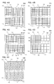
- FIG. 4A to 4E are conceptual diagrams illustrating the spatial arrangement of the magnetoresistive elements in the element array.
- 5A and 5B are enlarged views for explaining a tunnel magnetoresistive element constituting the magnetic sensor. It is a figure explaining the relationship between the voltage concerning a tunnel magnetoresistive element, and a sensitivity. It is a figure explaining the relationship between the insulating layer film thickness of a tunnel magnetoresistive element, and TMR ratio.
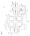
- the magnetic sensor 10 shown in FIG. 1 is a complex circuit, and detects a very small magnetic field intensity at room temperature or lower, such as a biomagnetic field.
- the magnetic sensor 10 includes a bridge circuit VC, a voltage control circuit CC, a correction circuit SC, and an output circuit OC.
- the voltage control circuit CC, the correction circuit SC, and the output circuit OC are a driving electric circuit 30.
- the bridge circuit VC has a Wheatstone bridge type circuit configuration and includes an element array 10a including a plurality of tunneling magnetoresistive elements (TMR elements) 20 and a fixed resistor 10b.
- the fixed resistor 10b is an element having a fixed resistance value, and has little temperature and other environmental fluctuations.
- the magnetic sensor 10 is composed of one element array 10a and three fixed resistors 10b, but may be composed of two or more element arrays 10a.
- the bridge circuit VC can be constituted by, for example, two element arrays 10a arranged in series and two fixed resistors 10b arranged in series.
- the bridge circuit VC can be configured with four element arrays 10a by adjusting the sensitivity direction of the element array 10a.
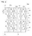
- the element array 10 a constituting the bridge circuit VC in the magnetic sensor 10 of FIG. 1 is configured by both a series connection and a parallel connection of a plurality of tunnel magnetoresistive elements 20.
- the some tunnel magnetoresistive element 20 can be combined suitably, the sensitivity of the magnetic sensor 10 can be improved, and noise can be reduced.
- the adjacent tunnel magnetoresistive elements 20 are arranged in the same direction and connected in series by the wiring 11 to form a magnetoresistive element group 20a.
- the element array 10a includes 20 or more and 10,000 or less tunnel magnetoresistive elements 20 connected in series.
- the number of tunnel magnetoresistive elements 20 By setting the number of tunnel magnetoresistive elements 20 to 20 or more, it is possible to effectively improve sensitivity and reduce noise with respect to detection of extremely weak magnetic fields.
- the cost can be reduced while avoiding an increase in size.
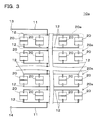
- the tunnel magnetoresistive elements 20 are connected in parallel to form a magnetoresistive element group 20a, and a plurality of parallel connected magnetoresistive element groups 20a are connected in series. Good.
- the wiring 11 can also be arranged in a zigzag shape. This increases the degree of freedom within the allowable space of the element array 10a.
- the tunnel magnetoresistive element 20 can be connected in series and in parallel even in a configuration in which the electrodes 13 and 14 are concentrated on one side.
- tunnel magnetoresistive element 20 is not limited to a rectangle, for example, as shown in FIG. 4E, an element array 10a in which circular tunnel magnetoresistive elements 20 are combined may be used.
- the above explanation is an example when the spatial arrangement of the tunnel magnetoresistive element 20 is considered as a plane.
- the number of arrayed silicon wafers in the height direction can be secured by stacking a plurality of deposited silicon wafers. It may be configured to.
- the element array 10 a is connected to the high potential side of the voltage control circuit 31 shown in FIG. 1 through one electrode 13 and connected to the output circuit OC on the detection side through the other electrode 14.
- the resistance value of the tunnel magnetoresistive element 20 changes due to the influence of the magnetic field.
- the potential of the electrode 14 of the element array 10a changes, and as a result, the output of the entire magnetic sensor 10 also changes.
- the magnetic field can be detected as will be described in detail later.
- a large number of magnetoresistive element groups 20a can secure current, and the detection output of the magnetic sensor 10 can be stabilized.
- the resistance value of the element array 10a is not less than 0.1 k ⁇ and not more than 10 k ⁇ .
- the voltage applied to the element array 10a is not less than 0.1V and not more than 20V. If the resistance value and voltage are within the above ranges, it is a relatively general range of the sensor circuit, and a general-purpose amplifier circuit, voltage source, etc. are utilized as components of the electric circuit 30 of the magnetic sensor 10. This makes it easy to detect signals with high accuracy with a simple circuit.
- each tunnel magnetoresistive element 20 includes a pinned magnetic layer 21, a free magnetic layer 22, and an insulating layer 23 provided between the pinned magnetic layer 21 and the free magnetic layer 22. And have. Electrodes 24 are provided at both ends of the tunnel magnetoresistive element 20, and the electrodes 24 are connected to the wiring 11 (or the wiring 12).
- the magnetization direction of the pinned magnetic layer 21 is fixed, and the magnetization direction of the free magnetic layer 22 changes under the influence of magnetic flux from the outside.
- the insulating layer 23 changes the tunnel current flowing from the pinned magnetic layer 21 to the free magnetic layer 22 according to the angle difference between the magnetization direction of the pinned magnetic layer 21 and the magnetization direction of the free magnetic layer 22. That is, the resistance value of the tunnel magnetoresistive element 20 changes according to the change of the magnetic flux passing through the tunnel magnetoresistive element 20.
- the plurality of tunnel magnetoresistive elements 20 constituting the same are arranged in the same direction, and the magnetization direction of the fixed magnetic layer 21 of the plurality of tunnel magnetoresistive elements 20 is substantially the same.
- the magnetization direction of the fixed magnetic layer 21 of the plurality of tunnel magnetoresistive elements 20 is substantially the same.
- the magnetization direction is within a range that does not hinder the measurement of biomagnetism. It only needs to have the same orientation.
- the free magnetic layer 22 in a state where the magnetic field of the plurality of tunneling magnetoresistive elements 20 is not applied.
- the directions of the magnetizations of these also substantially coincide with each other.
- the magnetization direction of the free magnetic layer 22 only needs to be aligned within a range that does not hinder biomagnetism measurement.
- the magnetization direction S of the pinned magnetic layer 21 of the tunnel magnetoresistive element 20 shown in FIGS. 5A and 5B is parallel to the + x direction.
- the magnetization direction F1 of the free magnetic layer 22 in a state where no magnetic field is applied to the tunnel magnetoresistive element 20 is parallel to a direction different from the magnetization direction S of the pinned magnetic layer 21, specifically, to the orthogonal + y direction. .
- the free magnetic layer 22 is magnetized along a specific direction.
- FIG. 5A when a magnetic field H is applied in the same direction as the pinned magnetic layer 21, the magnetization direction F 2 of the free magnetic layer 22 of the tunnel magnetoresistive element 20 is indicated by the arrow A that is the same direction as the pinned magnetic layer 21. Swing in the direction.
- FIG. 5B when a magnetic field H is applied in the opposite direction to the pinned magnetic layer 21, the magnetization direction F ⁇ b> 3 of the free magnetic layer 22 of the tunnel magnetoresistive element 20 is an arrow that is in the opposite direction to the pinned magnetic layer 21. Swings in direction B.
- the tunnel magnetoresistive element 20 when the magnetization direction of the free magnetic layer 22 swings in the same direction as the magnetization direction of the pinned magnetic layer 21, the tunnel current increases, the resistance value of the insulating layer 23 decreases, and the opposite direction When the voltage swings, the tunnel current decreases and the resistance value of the insulating layer 23 increases. Therefore, the resistance value of tunneling magneto-resistance element 20 shown in FIG. 5A decreases, and the resistance value of tunneling magneto-resistance element 20 shown in FIG. 5B increases.
- the resistance value of the tunnel magnetoresistive element 20 changes in a predetermined range according to the strength of the magnetic field H.
- the resistance of the entire element array 10a in which the tunnel magnetoresistive elements 20 are integrated in series changes, and the potential between the electrodes 13 and 14 of the element array 10a changes.
- the potential between the electrodes 13 and 14 of the element array 10a is detected as a potential difference of the bridge circuit VC in FIG. 1, and the output (specifically, the output voltage) of the magnetic sensor 10 is changed to obtain a magnetic detection signal.
- the pinned magnetic layer 21 is made of, for example, CoFeB, CoFe, or the like.
- the free magnetic layer 22 is made of, for example, NiFe, CoFe, CoNiFe, CoZrNb, or the like.
- each tunnel magnetoresistive element 20 (substantially the voltage applied to the insulating layer 23) is not less than 0.1 mV and not more than 50 mV. As already described, the tunnel magnetoresistive element 20 changes the tunnel resistance of the insulating layer 23 under the influence of the external magnetic field.
- each tunnel magnetoresistive element 20 (substantially the voltage applied to the insulating layer 23) is 50 mV or less, the sensitivity of each tunnel magnetoresistive element 20 is substantially improved, Noise generated in the tunnel magnetoresistive element 20 can be reduced.
- the voltage applied to the insulating layer 23 of each tunnel magnetoresistive element 20 is set to 0.1 mV or more, it is possible to prevent an excessive increase in the number of series or parallel numbers of the tunnel magnetoresistive elements 20, and tunnel magnetism. This also increases the reliability of the resistance element 20 such as the yield rate.
- FIG. 6 is a chart showing the relationship between the voltage applied to the tunnel magnetoresistive element 20 and the sensitivity.
- the horizontal axis represents the applied voltage or bias voltage (mV) to the tunnel magnetoresistive element 20, and the vertical axis represents the ratio between the detected potential difference (mV) and the strength of the external magnetic field ( ⁇ T).
- the detected potential difference (mV) is a potential difference obtained by looking at the potential difference generated on the bridge circuit when the tunnel magnetoresistive element 20 receives an external magnetic field and changes its resistance value through an amplifier having an appropriate amplification factor. is there.
- the amplification factor of the amplifier is set so as to obtain an easy-to-handle output (for example, an output of several hundred mV to 1V) according to the performance of the tunnel magnetoresistive element 20 and the detected magnetic field strength.
- an easy-to-handle output for example, an output of several hundred mV to 1V
- samples having different numbers of tunnel magnetoresistive elements 20 in series are plotted as samples.
- the sensitivity performance improves as the voltage applied to the insulating layer 23 is decreased. This is probably because the insulating layer 23 as a barrier layer is thin, so that a bias effect may be generated even with a small voltage (about several tens of mV).
- the voltage applied to the tunnel magnetoresistive element 20 (substantially the voltage applied to the insulating layer 23) is 0.5 mV or more and 20 mV or less. In this case, the sensitivity improvement and noise reduction of the tunnel magnetoresistive element 20 become more reliable, and the highly reliable tunnel magnetoresistive element 20 can be manufactured relatively easily.
- the resistance value per unit area of the insulating layer 23 is 1 ⁇ 10 3 ⁇ / ⁇ m 2 or more and 1 ⁇ 10 12 ⁇ / ⁇ m 2 or less.
- the resistance value is set to the lower limit of 1 ⁇ 10 3 ⁇ / ⁇ m 2 or more.
- the film thickness can be secured to some extent to suppress occurrence of a short circuit, and the resistance value is set to the upper limit of 1 ⁇ 10 12 ⁇ / ⁇ m 2 or less.
- the generation of the tunnel current can be secured and the sensitivity reduction of the tunnel magnetoresistive element 20 can be prevented.
- the film thickness of the insulating layer 23 is, for example, about 1.0 to 3.0 nm.
- the TMR ratio can be increased as the film thickness increases.
- the TMR ratio is defined as (R2 ⁇ R1) / R1 ⁇ 100 (%).
- the value R1 is a resistance value when the magnetization direction of the pinned magnetic layer 21 and the magnetization direction of the free magnetic layer 22 are the same direction (referred to as a parallel state)
- the value R2 is the magnetization value of the pinned magnetic layer 21.
- the direction of magnetization of the free magnetic layer 22 are opposite directions (referred to as an antiparallel state).
- FIG. 7 is a diagram illustrating the relationship between the thickness of the insulating layer 23 and the TMR ratio when the insulating layer 23 is formed of magnesium oxide (MgO).
- MgO magnesium oxide
- the area of the insulating layer 23 is 1 ⁇ m 2 or more and 1 mm 2 or less.
- the area of the insulating layer 23 is an area in a direction perpendicular to the film thickness direction of the insulating layer 23.
- the area of the insulating layer 23 is preferably 25 ⁇ m 2 or more and 0.04 mm 2 or less.
- the insulating layer 23 is made of a material having a coherent tunnel effect.
- the TMR ratio can be increased by the coherent tunnel effect, and the sensitivity of the tunnel magnetoresistive element 20 and the element array 10a can be increased.
- the insulating layer 23 is formed of any one of magnesium oxide, spinel, and aluminum oxide.
- the voltage applied to the bridge circuit VC or the voltage applied to the magnetic sensor 10 is constant and the number of tunnel magnetoresistive elements 20 in series is increased, the voltage applied to one tunnel magnetoresistive element 20 is increased in series. That means it gets smaller.
- the size S v of the 1 / f noise of tunneling magneto-resistance element 20 is given by the following representative formula (1).
- (alpha) is a coefficient
- V is the voltage (element voltage) of one tunnel magnetoresistive element 20
- A is an element area
- f is a frequency. That is, the voltage component of the noise generated in the single tunneling magneto-resistance element 20, when only the element voltage V is a variable, considered to be proportional to the square root That element voltage V of the noise magnitude S v.
- the noise reduction effect by effectively increasing the element area A by increasing the parallel number of the tunnel magnetoresistive elements 20 with a constant bridge voltage can be expected to be the same as the noise reduction by the series connection. From the above, the larger the number of series and parallel connections, the better the noise reduction effect can be expected (dispersion of device voltage and expansion of device area). desirable.
- the electric circuit 30 for driving the bridge circuit VC includes the voltage control circuit CC, the correction circuit SC, and the output circuit OC as already described.
- a voltage is applied to the bridge circuit VC by connecting the voltage control circuit CC of the electric circuit 30 and the correction circuit SC. That is, the electric circuit 30 applies a voltage to the element array 10a (and thus the plurality of tunneling magnetoresistive elements 20) and the fixed resistor 10b constituting the bridge circuit VC.
- the voltage control circuit CC of the electric circuit 30 has a power supply unit 31a and is a reference with respect to one end of a pair of series units D1 and D2 constituting a bridge circuit VC including one or more element arrays 10a. Apply voltage.
- the correction circuit SC includes a feedback unit 32 and a correction unit 33, and applies an offset voltage to the other end of one series unit D2 constituting the bridge circuit VC. That is, only the reference voltage output from the voltage control circuit CC is applied to one series part D1 of the bridge circuit VC, and the other series part D2 of the bridge circuit VC is output from the voltage control circuit CC. The reference voltage and the correction voltage output from the correction circuit SC are applied.
- the correction circuit SC applies a voltage signal obtained from the potential difference between the detection terminals P1 and P2 of the bridge circuit VC, that is, an offset voltage, to one end of the series part D2, so that the potential difference between the detection terminals P1 and P2 of the bridge circuit VC is obtained. Operates to counteract.
- the differential amplification signal from the amplification unit 34 of the output circuit OC described later is input to the feedback unit 32.
- the feedback unit 32 actually includes a low-pass filter or the like, and feeds back to the correction unit 33 a voltage signal composed of a low-frequency component obtained by removing a high-frequency component from a differential amplification signal corresponding to the potential difference between the detection terminals P1 and P2.
- the correction unit 33 Based on the voltage signal input from the feedback unit 32, the correction unit 33 cancels the potential difference between the detection terminals P1 and P2 with respect to the ground side (that is, the fixed resistor 10b) of the series unit D2 of the bridge circuit VC.
- Such a voltage signal that is, an offset voltage is applied.
- control is performed so that the voltage difference between the detection terminals P1 and P2 of the bridge circuit VC is equal to or less than a certain reference value (for example, 0 V) with respect to the DC component or the extremely low frequency component.
- a certain reference value for example, 0 V
- the amplification factor in the amplification unit 34 can be set high. Further, for example, it is possible to cancel the potential difference between the bridge circuits VC, which is caused by the environmental temperature or environmental disturbance and fluctuates irrespective of the magnetic field to be detected.
- the voltage difference between the detection terminals P1 and P2 of the bridge circuit VC is changed. Adjustment can be easily performed so that the average value becomes a target value (for example, 0 V).
- the output circuit OC has an amplifying unit 34 and a filter unit 35.
- the amplifying unit 34 amplifies an output signal, that is, a potential difference between the detection terminals P1 and P2 of the bridge circuit VC.
- a differential amplifier 34a configured by an operational amplifier or the like is used as the amplifying unit 34. That is, the voltage difference between the detection terminals P1 and P2 of the bridge circuit VC is extracted as an analog voltage amplification signal via the difference amplifier 34a.
- the filter unit 35 includes either a low-pass filter, a high-pass filter, or both a low-pass filter and a high-pass filter that selectively pass only a component corresponding to a magnetic signal in a predetermined band from the amplified signal from the amplification unit 34.
- a filter unit 35 for example, an active type band amplifier 35a or the like is used, but a passive type band filter can also be used.
- the voltage amplification signal from the differential amplifier 34a is input to the filter unit 35, and after removing an unnecessary frequency band signal, a signal value of a voltage narrowed to a frequency band corresponding to the magnetic field to be detected is output.
- the magnetic sensor in order to increase the signal strength, there are measures such as making the magnetic sensor have a structure that increases the tunnel magnetoresistance effect, or increasing the voltage applied to the magnetic sensor. In order to reduce the noise, there are measures such as integrating the tunnel magnetoresistive elements in the magnetic sensor or lowering the voltage applied to the magnetic sensor.
- the tunneling magnetoresistive effect as a magnetic sensor tends to decrease due to performance variations between elements and the inclusion of defective elements.
- the voltage applied to the magnetic sensor is a trade-off between sensitivity performance and noise performance, and it is difficult to make the magnetic sensor optimally configured.
- the magnetic sensor 10 is integrated with a plurality of tunnel magnetoresistive elements 20, and the voltage applied to each tunnel magnetoresistive element 20 is set to 1.0 mV or more and 50 mV or less,
- the magnetic sensor 10 has a structure that can secure high sensitivity performance while greatly reducing noise, and can have excellent magnetic resolution.
- Example 1 design values of the magnetic sensor 10 of Example 1 are shown.
- the magnetic sensor 10 according to the first embodiment is a high magnetic resolution type sensor.
- the magnetic sensor 10 of Example 1 has a relatively large noise reduction effect.
- Magnetic sensor resistance 1.04 k ⁇ Magnetic sensor area (approximate): 49.73 mm 2 Magnetic sensor width (as square): 7.05mm Bridge circuit voltage (voltage applied to magnetic sensor): 8V Number of TMR elements in series: 1110 Number of parallel TMR elements: 5 rows Insulating layer thickness: 1.35 nm Resistance value per unit area of insulating layer: 3 ⁇ 10 4 ⁇ / ⁇ m 2 TMR element dimensions (vertical): 80 ⁇ m TMR element dimensions (horizontal): 80 ⁇ m Area of TMR element (area of insulating layer): 6400 ⁇ m 2 Resistance of TMR element: 4.69 ⁇ Voltage applied to TMR element: 3.6 mV
- Example 2 design values of the magnetic sensor 10 of Example 2 are shown.
- the magnetic sensor 10 of Example 2 is a high spatial resolution type sensor.
- the tunnel magnetoresistive elements 20 are arranged at a high density, and the size is relatively small.
- Magnetic sensor resistance 1.42 k ⁇ Magnetic sensor area: (approximate) 2.28 mm 2 Magnetic sensor width: 1.51mm (as square)
- Bridge circuit voltage (voltage applied to magnetic sensor): 8V
- Number of TMR elements in series 340
- Number of TMR elements in parallel 12 rows
- Insulating layer thickness 1.2 nm Resistance value per unit area of insulating layer: 2 ⁇ 10 4 ⁇ / ⁇ m 2
- Example 3 design values of the magnetic sensor 10 of Example 3 are shown.
- the magnetic sensor 10 of Example 3 satisfies the effects of the present embodiment even when the insulating layer 23 is relatively thick.
- Magnetic sensor resistance value 1.11 k ⁇ Magnetic sensor area (approximate): 3.94 mm 2
- Bridge circuit voltage 0.5V
- Number of TMR elements in series 25
- Number of parallel TMR elements 5 rows
- Insulating layer thickness 2.2 nm
- Resistance value per unit area of insulating layer 5 ⁇ 10 6 ⁇ / ⁇ m 2
- TMR element size vertical
- TMR element dimensions 150 ⁇ m
- the magnetic sensor included in the sensor unit and the like of the second embodiment is an application of the magnetic sensor of the first embodiment, and matters not specifically described are the same as those of the first embodiment.
- the magnetic detection device 300 includes at least one sensor unit 200 and a control unit 40.
- the sensor unit 200 is connected to the control unit 40 via the wiring unit 15.
- the sensor unit 200 is formed by connecting the above-described plurality of magnetic sensors 10 (see FIG. 1) by connecting them in series.
- one magnetic sensor 10 is illustrated in a cylindrical shape.
- the magnetic detection device 300 in the magnetic detection device 300, four magnetic sensors 10 are arranged in a straight line and connected in series to form one sensor unit 200, and a plurality of sensor units 200 are arranged adjacently in parallel. ing.
- the magnetic sensors 10 may be connected only by parallel connection or by both serial connection and parallel connection.
- the control unit 40 includes a signal detection unit 41, a storage unit 42, an input / output unit 43, and a main control unit 44.
- the signal detection unit 41 in the control unit 40 receives the detection signal output from each sensor unit 200 under the control of the main control unit 44.
- the signal detection unit 41 for example, a magnetic signal in a predetermined band input and detected from each sensor unit 200 is changed into a form that can be easily processed.
- the magnetic signal from the sensor unit 200 is an analog signal and is converted into a digital signal by the signal detection unit 41 for processing by the main control unit 44.
- the storage unit 42 stores a predetermined program and data for operating the main control unit 44.
- the storage unit 42 stores the magnetic signal digitally converted by the signal detection unit 41 under the control of the main control unit 44.
- the magnetic signal obtained from each sensor unit 200 can be stored as detection data in association with each sensor unit 200, and such time-dependent detection data is sequentially recorded in time series.
- the storage unit 42 also stores the result of mapping the measured magnetic signal in accordance with an instruction from the main control unit 44 operating based on the program or an operator instruction via the input / output unit 43. be able to.
- the input / output unit 43 causes the main control unit 44 to start an operation according to a predetermined program in response to an operator instruction, or causes the signal detection unit 41 to read the detection result of the sensor unit 200 by the operation of the main control unit 44. It is stored in the storage unit 42.
- the input / output unit 43 operates under the control of the main control unit 44 and displays the magnetic measurement result obtained from the detection result of the sensor unit 200 on, for example, a display.
- the main control unit 44 controls the operations of the signal detection unit 41, the storage unit 42, and the input / output unit 43 in an integrated manner.
- the main control unit 44 can perform processing such as filtering and enhancement on the magnetic signal obtained through the signal detection unit 41. Further, the main control unit 44 can edit the magnetic signal obtained via the signal detection unit 41. Specifically, the magnetic signal data obtained from each sensor unit 200 is two-dimensionally mapped, or the change over time is converted into a video image, and the result is displayed on the input / output unit 43. it can.
- the sensitivity is improved and the noise is reduced.
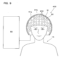
- the living body magnetic measurement device 400 includes a living body magnetic field detection unit 50 and a control unit 60.
- the biomagnetic field detection unit 50 is arranged under the influence of a magnetic field from a living body and extracts a weak magnetic field from the living body as a magnetic signal.
- the biomagnetic field detection unit 50 includes a large number of sensor units 200 similar to those shown in FIG. 8 (that is, a combination of a plurality of magnetic sensors 10 (see FIG. 1)). It has the structure which was arranged.
- the plurality of sensor units 200 can be configured such that their arrangement surfaces are curved along the surface of a living body that is a detection target. In the example of FIG.
- the sensor unit 200 includes, for example, a helmet-type magnetic shield device 51 that includes a shield part 51 a that covers the periphery and a main body 51 b that is disposed inside the shield part 51 a and supports a large number of sensor units 200. It is built in and curved along the head of the subject HS.
- the biomagnetic field detector 50 is mounted on the head of the subject HS and detects the biomagnetism of the subject HS.
- the control unit 60 performs signal processing on the output of the biomagnetic field detection unit 50.
- the control unit 60 performs the same operation as the control unit 40 of the magnetic detection device 300 described in the second embodiment.
- the magnetic measurement device 400 has the above-described magnetic sensor 10 and thus has an effect of improving biosensitivity and reducing noise. Since the magnetic sensor 10 is fine, if the magnetic sensors 10 are two-dimensionally or three-dimensionally arranged with high density, spatial resolution can be improved and high accuracy can be achieved.
- the weak magnetic field from a living body is, for example, about tens of pT due to the heart and about 100 pT due to brain function.
- the biosensitivity necessary for detecting this magnetic field will be described.
- the voltage applied to each element array 10a becomes 1V.
- a magnetic field of 1 pT 1,000 times 1fT
- a voltage difference of 1 mV is generated on the bridge circuit VC.
- the noise has a performance of about 1 ⁇ V
- a brain magnetic field of about 100 pT for example, can be detected with a good SN ratio.
- the biosensitivity when a signal is detected under the above conditions is 1 mV / 1 pT in voltage notation, and 0.1% / 1 pT in TMR ratio (ie, rate of change in resistance value) notation.
- the magnetic sensor according to the present invention is not limited to the above.
- the arrangement of the tunnel magnetoresistive elements 20 can be changed as appropriate according to the application.
- the magnetization direction of the pinned magnetic layer 21 of the tunnel magnetoresistive element 20 or the magnetization direction of the free magnetic layer 22 can be changed as appropriate.
- the amplification unit 34 and the filter unit 35 are provided in the electric circuit 30, but it is not necessary to provide them.
- the magnetic sensor 10 includes a plurality of element arrays 10a in which the magnetization direction of the fixed magnetic layer 21 or the magnetization direction of the free magnetic layer 22 is different, for example, with the element array 10a that is an integrated body as one unit. It is configured by combining.
- the magnetic detection device 300 is configured by the sensor unit 200, but may be configured by one magnetic sensor 10.
Landscapes
- Physics & Mathematics (AREA)
- Condensed Matter Physics & Semiconductors (AREA)
- General Physics & Mathematics (AREA)
- Measuring Magnetic Variables (AREA)
- Hall/Mr Elements (AREA)
Abstract
Description
以下、図面を参照しつつ、本発明に係る第1実施形態の磁気センサーについて説明する。


(実施例1)
以下、実施例1の磁気センサー10の設計値を示す。実施例1の磁気センサー10は、高磁気分解能タイプのセンサーである。実施例1の磁気センサー10は、ノイズ低減効果が比較的大きくなっている。
磁気センサー抵抗値:1.04kΩ
磁気センサー面積(概算):49.73mm2
磁気センサー幅(正方形として):7.05mm
ブリッジ回路電圧(磁気センサーにかかる電圧):8V
TMR素子直列数:1110個
TMR素子並列数:5列
絶縁層膜厚:1.35nm
絶縁層の単位面積あたりの抵抗値:3×10⁴Ω/μm2
TMR素子寸法(縦):80μm
TMR素子寸法(横):80μm
TMR素子の面積(絶縁層の面積):6400μm2
TMR素子の抵抗:4.69Ω
TMR素子にかかる電圧:3.6mV
以下、実施例2の磁気センサー10の設計値を示す。実施例2の磁気センサー10は、高空間分解能タイプのセンサーである。実施例2の磁気センサー10は、トンネル磁気抵抗素子20が高密度に配置され、サイズが比較的小さくなっている。
磁気センサー抵抗値:1.42kΩ
磁気センサー面積:(概算)2.28mm2
磁気センサー幅:(正方形として)1.51mm
ブリッジ回路電圧(磁気センサーにかかる電圧):8V
TMR素子直列数:340個
TMR素子並列数:12列
絶縁層膜厚:1.2nm
絶縁層の単位面積あたりの抵抗値:2×10⁴Ω/μm2
TMR素子寸法(縦):20μm
TMR素子寸法(横):20μm
TMR素子の面積(絶縁層の面積):400μm2
TMR素子の抵抗:50.00Ω
TMR素子にかかる電圧:11.8mV
以下、実施例3の磁気センサー10の設計値を示す。実施例3の磁気センサー10は、絶縁層23の膜厚が比較的厚くても本実施形態の効果を満たすものとなっている。
磁気センサー抵抗値:1.11kΩ
磁気センサー面積(概算):3.94mm2
磁気センサー幅(正方形として):1.98mm
ブリッジ回路電圧:0.5V
TMR素子直列数:25個
TMR素子並列数:5列
絶縁層膜厚:2.2nm
絶縁層の単位面積あたりの抵抗値:5×10⁶Ω/μm2
TMR素子寸法(縦):150μm
TMR素子寸法(横):150μm
TMR素子の面積(絶縁層の面積):22500μm2
TMR素子の抵抗:222.22Ω
TMR素子にかかる電圧:10.0mV
以下、第2実施形態に係るセンサーユニット及び磁気検出装置について説明する。なお、第2実施形態のセンサーユニット等に含まれる磁気センサーは第1実施形態の磁気センサーを応用したものであり、特に説明しない事項は第1実施形態と同様である。
以下、第3実施形態に係る磁気計測装置について説明する。なお、第3実施形態の磁気計測装置に含まれる磁気センサー及びセンサーユニットは第1及び第2実施形態の磁気センサー等を応用又は変形したものであり、特に説明しない事項は第1及び第2実施形態と同様である。
Claims (16)
- 固定磁性層と、自由磁性層と、前記固定磁性層及び前記自由磁性層間に設けられた絶縁層とをそれぞれ有し、外界磁場の影響で前記絶縁層のトンネル抵抗をそれぞれ変化させる複数のトンネル磁気抵抗素子を含む素子アレイと、
前記素子アレイを構成する前記複数のトンネル磁気抵抗素子に電圧を印加する電気回路とを備え、
各トンネル磁気抵抗素子に印加される電圧が、0.1mV以上50mV以下である、磁気センサー。 - 前記各トンネル磁気抵抗素子に印加される電圧が、0.5mV以上20mV以下である、請求項1に記載の磁気センサー。
- 前記素子アレイは、前記複数のトンネル磁気抵抗素子の、直列接続、並列接続、又は直列接続及び並列接続の両方によって構成されている、請求項1及び2のいずれか一項に記載の磁気センサー。
- 前記素子アレイは、直列接続された20個以上10000個以下の前記トンネル磁気抵抗素子を含む、請求項1~3のいずれか一項に記載の磁気センサー。
- 前記素子アレイの抵抗値は、0.1kΩ以上10kΩ以下である、請求項1~4のいずれか一項に記載の磁気センサー。
- 各トンネル磁気抵抗素子の前記絶縁層の単位面積あたりの抵抗値は、1×10³Ω/μm2以上1×1012Ω/μm2以下である、請求項1~5のいずれか一項に記載の磁気センサー。
- 前記絶縁層は、コヒーレントトンネル効果をもつ材料で形成されている、請求項1~6のいずれか一項に記載の磁気センサー。
- 前記絶縁層は、酸化マグネシウム、スピネル、及び酸化アルミニウムのいずれか1つで形成されている、請求項1~7のいずれか一項に記載の磁気センサー。
- 各トンネル磁気抵抗素子の前記絶縁層の面積は、1μm2以上1mm2以下である、請求項1~8のいずれか一項に記載の磁気センサー。
- 前記素子アレイに印加される電圧は、0.1V以上20V以下である、請求項1~9のいずれか一項に記載の磁気センサー。
- 前記電気回路は、前記素子アレイを1つ以上含むブリッジ回路を構成する一対の直列部に対して基準電圧を印加する電源部と、前記ブリッジ回路を構成する一方の直列部に対してオフセット電圧を印加する補正部と、前記ブリッジ回路の検出端子間の出力信号から得た信号を前記補正部にフィードバックするフィードバック部とを有する、請求項1~10のいずれか一項に記載の磁気センサー。
- 前記電気回路は、前記ブリッジ回路の検出端子間の出力信号を増幅する増幅部と、前記増幅部からの増幅信号から所定の帯域の磁気信号成分を通過させるローパスフィルター、ハイパスフィルター、又はローパスフィルター及びハイパスフィルターの両方を有するフィルター部とを備える、請求項1~11のいずれか一項に記載の磁気センサー。
- 請求項1~12のいずれか一項に記載の複数の磁気センサーを、直列接続、並列接続、又は直列接続及び並列接続の両方によって連結して一体化した、センサーユニット。
- 請求項1~12のいずれか一項に記載の少なくとも1つの磁気センサーと、前記少なくとも1つの磁気センサーからの検出出力を信号処理する制御部とを備える、磁気検出装置。
- 請求項1~12のいずれか一項に記載の複数の磁気センサーを有し生体からの磁場の影響下に配置される生体磁場検出部と、前記生体磁場検出部の出力を信号処理する制御部とを備える、生体用の磁気計測装置。
- 100pT以下の磁界を計測する、請求項15に記載の生体用の磁気計測装置。
Priority Applications (4)
| Application Number | Priority Date | Filing Date | Title |
|---|---|---|---|
| US16/065,539 US10830840B2 (en) | 2015-12-28 | 2016-12-28 | Magnetic sensor, sensor unit, magnetic detection device, and magnetic measurement device |
| EP16881813.6A EP3399324B1 (en) | 2015-12-28 | 2016-12-28 | Magnetic sensor, sensor unit, magnetic detection device, and magnetic measurement device |
| JP2017559234A JPWO2017115839A1 (ja) | 2015-12-28 | 2016-12-28 | 磁気センサー、センサーユニット、磁気検出装置、及び磁気計測装置 |
| CN201680076140.4A CN108431620B (zh) | 2015-12-28 | 2016-12-28 | 磁性传感器、传感器单元、磁性检测装置、以及磁性测量装置 |
Applications Claiming Priority (2)
| Application Number | Priority Date | Filing Date | Title |
|---|---|---|---|
| JP2015-256150 | 2015-12-28 | ||
| JP2015256150 | 2015-12-28 |
Publications (1)
| Publication Number | Publication Date |
|---|---|
| WO2017115839A1 true WO2017115839A1 (ja) | 2017-07-06 |
Family
ID=59224903
Family Applications (1)
| Application Number | Title | Priority Date | Filing Date |
|---|---|---|---|
| PCT/JP2016/089053 Ceased WO2017115839A1 (ja) | 2015-12-28 | 2016-12-28 | 磁気センサー、センサーユニット、磁気検出装置、及び磁気計測装置 |
Country Status (5)
| Country | Link |
|---|---|
| US (1) | US10830840B2 (ja) |
| EP (1) | EP3399324B1 (ja) |
| JP (1) | JPWO2017115839A1 (ja) |
| CN (1) | CN108431620B (ja) |
| WO (1) | WO2017115839A1 (ja) |
Cited By (5)
| Publication number | Priority date | Publication date | Assignee | Title |
|---|---|---|---|---|
| CN109009065A (zh) * | 2018-06-05 | 2018-12-18 | 上海理工大学 | 基于tmr弱磁传感器阵列的脑磁信息检测系统及方法 |
| CN111868541A (zh) * | 2018-05-18 | 2020-10-30 | 株式会社东海理化电机制作所 | 磁传感器装置 |
| JP2022021112A (ja) * | 2020-07-21 | 2022-02-02 | Tdk株式会社 | 磁気センサ |
| CN116424161A (zh) * | 2023-03-21 | 2023-07-14 | 国能新朔铁路有限责任公司 | 重载铁路钢轨电位和牵引回流的确定方法、装置及设备 |
| WO2024101254A1 (ja) * | 2022-11-09 | 2024-05-16 | ソニーセミコンダクタソリューションズ株式会社 | 磁気検出装置及びデコーディングシステム |
Families Citing this family (10)
| Publication number | Priority date | Publication date | Assignee | Title |
|---|---|---|---|---|
| JP6724459B2 (ja) * | 2016-03-23 | 2020-07-15 | Tdk株式会社 | 磁気センサ |
| US11908177B2 (en) * | 2019-05-29 | 2024-02-20 | Nec Corporation | Updated learning of feature extraction model that extracts moving image feature amount from moving image data and still image feature amount from still image data |
| US11169228B2 (en) * | 2019-08-27 | 2021-11-09 | Western Digital Technologies, Inc. | Magnetic sensor with serial resistor for asymmetric sensing field range |
| US11169226B2 (en) * | 2019-08-27 | 2021-11-09 | Western Digital Technologies, Inc. | Magnetic sensor bias point adjustment method |
| US11169227B2 (en) * | 2019-08-28 | 2021-11-09 | Western Digital Technologies, Inc. | Dual free layer TMR magnetic field sensor |
| CN111596239B (zh) * | 2020-06-15 | 2021-07-20 | 北京航空航天大学 | 一种单片集成三轴隧穿磁电阻的磁传感器及其制备方法 |
| CN115200751A (zh) * | 2022-06-29 | 2022-10-18 | 江苏多维科技有限公司 | 一种基于隧道磁阻效应的触觉传感器 |
| CN115980639B (zh) * | 2022-12-15 | 2024-01-23 | 江苏多维科技有限公司 | 一种磁阻传感器 |
| US20250076442A1 (en) * | 2023-08-31 | 2025-03-06 | Texas Instruments Incorporated | Anisotropic magnetoresistance sensor circuit with adjustable offset trim |
| EP4597121A1 (en) * | 2024-01-30 | 2025-08-06 | LEM International SA | Current transducer with tmr magnetic field sensor |
Citations (9)
| Publication number | Priority date | Publication date | Assignee | Title |
|---|---|---|---|---|
| JP2001093119A (ja) * | 1999-09-24 | 2001-04-06 | Hitachi Ltd | トンネル磁気抵抗効果型磁気ヘッド及びその製造方法 |
| JP2008170368A (ja) * | 2007-01-15 | 2008-07-24 | Mitsubishi Electric Corp | 磁界検出装置および磁界検出装置の製造方法 |
| JP2011103336A (ja) * | 2009-11-10 | 2011-05-26 | Denso Corp | 磁気抵抗効果素子およびそれを用いたセンサ |
| WO2012014415A1 (ja) * | 2010-07-29 | 2012-02-02 | 株式会社日立製作所 | 岩塩構造薄膜をシードとして用いた低抵抗かつ高効率のスピン注入素子 |
| WO2012032962A1 (ja) * | 2010-09-10 | 2012-03-15 | コニカミノルタオプト株式会社 | 生体磁気計測装置、生体磁気計測システム、及び、生体磁気計測方法 |
| JP2012152515A (ja) * | 2011-01-28 | 2012-08-16 | Konica Minolta Holdings Inc | 磁気センサおよびそれを用いる生体磁気計測装置 |
| JP2013175615A (ja) * | 2012-02-27 | 2013-09-05 | National Institute For Materials Science | 強磁性トンネル接合体とそれを用いた磁気抵抗効果素子及びスピントロニクスデバイス |
| JP2015125019A (ja) * | 2013-12-25 | 2015-07-06 | 株式会社東芝 | 電流センサ、電流測定モジュール及びスマートメータ |
| WO2015146656A1 (ja) * | 2014-03-28 | 2015-10-01 | コニカミノルタ株式会社 | 磁気センサー |
Family Cites Families (11)
| Publication number | Priority date | Publication date | Assignee | Title |
|---|---|---|---|---|
| JPH11112054A (ja) | 1997-10-01 | 1999-04-23 | Fujitsu Ltd | 磁気センサー及びこの磁気センサーを使用した装置 |
| JP3835445B2 (ja) | 2001-01-24 | 2006-10-18 | ヤマハ株式会社 | 磁気センサ |
| JP4100025B2 (ja) * | 2002-04-09 | 2008-06-11 | ソニー株式会社 | 磁気抵抗効果素子及び磁気メモリ装置 |
| JP4084089B2 (ja) * | 2002-05-30 | 2008-04-30 | 株式会社ルネサステクノロジ | 薄膜磁性体記憶装置 |
| JP4042478B2 (ja) * | 2002-06-19 | 2008-02-06 | ソニー株式会社 | 磁気抵抗効果素子及び磁気メモリ装置 |
| JP4576791B2 (ja) * | 2002-12-27 | 2010-11-10 | Tdk株式会社 | メモリ装置 |
| US20060092689A1 (en) * | 2004-11-04 | 2006-05-04 | Daniel Braun | Reference current source for current sense amplifier and programmable resistor configured with magnetic tunnel junction cells |
| JP2006269907A (ja) * | 2005-03-25 | 2006-10-05 | Tdk Corp | トンネル磁気抵抗効果素子の検査方法及び装置、トンネル磁気抵抗効果素子の製造方法、並びにトンネル磁気抵抗効果素子 |
| JP5279357B2 (ja) * | 2008-06-12 | 2013-09-04 | キヤノン株式会社 | 複合粒子、その製造方法、分散液、磁気バイオセンシング装置および磁気バイオセンシング方法 |
| JP5434494B2 (ja) | 2009-11-10 | 2014-03-05 | 株式会社リコー | 磁気センサ |
| JP5861703B2 (ja) | 2011-05-20 | 2016-02-16 | コニカミノルタ株式会社 | 磁気センサ及び生体磁気計測システム |
-
2016
- 2016-12-28 JP JP2017559234A patent/JPWO2017115839A1/ja active Pending
- 2016-12-28 WO PCT/JP2016/089053 patent/WO2017115839A1/ja not_active Ceased
- 2016-12-28 CN CN201680076140.4A patent/CN108431620B/zh active Active
- 2016-12-28 EP EP16881813.6A patent/EP3399324B1/en active Active
- 2016-12-28 US US16/065,539 patent/US10830840B2/en active Active
Patent Citations (9)
| Publication number | Priority date | Publication date | Assignee | Title |
|---|---|---|---|---|
| JP2001093119A (ja) * | 1999-09-24 | 2001-04-06 | Hitachi Ltd | トンネル磁気抵抗効果型磁気ヘッド及びその製造方法 |
| JP2008170368A (ja) * | 2007-01-15 | 2008-07-24 | Mitsubishi Electric Corp | 磁界検出装置および磁界検出装置の製造方法 |
| JP2011103336A (ja) * | 2009-11-10 | 2011-05-26 | Denso Corp | 磁気抵抗効果素子およびそれを用いたセンサ |
| WO2012014415A1 (ja) * | 2010-07-29 | 2012-02-02 | 株式会社日立製作所 | 岩塩構造薄膜をシードとして用いた低抵抗かつ高効率のスピン注入素子 |
| WO2012032962A1 (ja) * | 2010-09-10 | 2012-03-15 | コニカミノルタオプト株式会社 | 生体磁気計測装置、生体磁気計測システム、及び、生体磁気計測方法 |
| JP2012152515A (ja) * | 2011-01-28 | 2012-08-16 | Konica Minolta Holdings Inc | 磁気センサおよびそれを用いる生体磁気計測装置 |
| JP2013175615A (ja) * | 2012-02-27 | 2013-09-05 | National Institute For Materials Science | 強磁性トンネル接合体とそれを用いた磁気抵抗効果素子及びスピントロニクスデバイス |
| JP2015125019A (ja) * | 2013-12-25 | 2015-07-06 | 株式会社東芝 | 電流センサ、電流測定モジュール及びスマートメータ |
| WO2015146656A1 (ja) * | 2014-03-28 | 2015-10-01 | コニカミノルタ株式会社 | 磁気センサー |
Non-Patent Citations (1)
| Title |
|---|
| See also references of EP3399324A4 * |
Cited By (8)
| Publication number | Priority date | Publication date | Assignee | Title |
|---|---|---|---|---|
| CN111868541A (zh) * | 2018-05-18 | 2020-10-30 | 株式会社东海理化电机制作所 | 磁传感器装置 |
| CN111868541B (zh) * | 2018-05-18 | 2023-03-31 | 株式会社东海理化电机制作所 | 磁传感器装置 |
| CN109009065A (zh) * | 2018-06-05 | 2018-12-18 | 上海理工大学 | 基于tmr弱磁传感器阵列的脑磁信息检测系统及方法 |
| CN109009065B (zh) * | 2018-06-05 | 2021-11-19 | 上海理工大学 | 基于tmr弱磁传感器阵列的脑磁信息检测系统及方法 |
| JP2022021112A (ja) * | 2020-07-21 | 2022-02-02 | Tdk株式会社 | 磁気センサ |
| JP7173104B2 (ja) | 2020-07-21 | 2022-11-16 | Tdk株式会社 | 磁気センサ |
| WO2024101254A1 (ja) * | 2022-11-09 | 2024-05-16 | ソニーセミコンダクタソリューションズ株式会社 | 磁気検出装置及びデコーディングシステム |
| CN116424161A (zh) * | 2023-03-21 | 2023-07-14 | 国能新朔铁路有限责任公司 | 重载铁路钢轨电位和牵引回流的确定方法、装置及设备 |
Also Published As
| Publication number | Publication date |
|---|---|
| US20190018083A1 (en) | 2019-01-17 |
| JPWO2017115839A1 (ja) | 2018-11-29 |
| EP3399324A1 (en) | 2018-11-07 |
| EP3399324A4 (en) | 2019-01-23 |
| EP3399324B1 (en) | 2022-04-13 |
| US10830840B2 (en) | 2020-11-10 |
| CN108431620A (zh) | 2018-08-21 |
| CN108431620B (zh) | 2021-04-09 |
Similar Documents
| Publication | Publication Date | Title |
|---|---|---|
| CN108431620B (zh) | 磁性传感器、传感器单元、磁性检测装置、以及磁性测量装置 | |
| US11350840B2 (en) | Magnetic sensor, biological cell sensing device, and diagnostic device | |
| US8933696B2 (en) | Magnetic sensor and biomagnetism measurement system | |
| US10514430B2 (en) | Magnetic sensor utilizing magnetization reset for sense axis selection | |
| CN103188992B (zh) | 生物磁场测量装置、生物磁场测量系统、以及生物磁场测量方法 | |
| US20180081001A1 (en) | Magnetic Sensor, Magnetic Sensor Device, and Diagnostic Device | |
| JP2008516225A (ja) | 非線形磁界センサ及び電流センサ | |
| JP2013535674A5 (ja) | ||
| CN205809273U (zh) | 一种无需置位/复位装置的各向异性磁电阻amr传感器 | |
| US11474168B2 (en) | Magnetic sensor device | |
| JP2019132719A (ja) | 磁気検出装置 | |
| JP2022031282A (ja) | 磁気センサ、生体細胞検出装置及び診断装置 | |
| JP2017166921A (ja) | 磁気センサおよび磁気センサ装置 | |
| CN206649142U (zh) | 一种可提高信噪比的阵列式磁敏传感器 | |
| US11009569B2 (en) | Magnetic field sensing device | |
| US20230093647A1 (en) | Magnetic sensor | |
| JP7482046B2 (ja) | 磁気センサ及び検査装置 | |
| CN115840176A (zh) | 磁传感器 | |
| JP2019174438A (ja) | 磁気検出装置 | |
| CN118409253B (zh) | 反常霍尔效应传感器、装置及线性磁场传感器系统 | |
| JP2012088225A (ja) | 磁気検出装置 | |
| JP7414703B2 (ja) | 磁気センサ及び検査装置 | |
| CN115840166A (zh) | 磁传感器 | |
| CN115840167A (zh) | 磁传感器 | |
| JP6735603B2 (ja) | 生体情報検出装置 |
Legal Events
| Date | Code | Title | Description |
|---|---|---|---|
| 121 | Ep: the epo has been informed by wipo that ep was designated in this application |
Ref document number: 16881813 Country of ref document: EP Kind code of ref document: A1 |
|
| ENP | Entry into the national phase |
Ref document number: 2017559234 Country of ref document: JP Kind code of ref document: A |
|
| NENP | Non-entry into the national phase |
Ref country code: DE |
|
| WWE | Wipo information: entry into national phase |
Ref document number: 2016881813 Country of ref document: EP |
|
| ENP | Entry into the national phase |
Ref document number: 2016881813 Country of ref document: EP Effective date: 20180730 |