WO2017119357A1 - 光発電素子 - Google Patents
光発電素子 Download PDFInfo
- Publication number
- WO2017119357A1 WO2017119357A1 PCT/JP2016/088848 JP2016088848W WO2017119357A1 WO 2017119357 A1 WO2017119357 A1 WO 2017119357A1 JP 2016088848 W JP2016088848 W JP 2016088848W WO 2017119357 A1 WO2017119357 A1 WO 2017119357A1
- Authority
- WO
- WIPO (PCT)
- Prior art keywords
- photovoltaic
- layer
- silicon dioxide
- fine particles
- dioxide fine
- Prior art date
- Legal status (The legal status is an assumption and is not a legal conclusion. Google has not performed a legal analysis and makes no representation as to the accuracy of the status listed.)
- Ceased
Links
Images


Classifications
-
- H—ELECTRICITY
- H01—ELECTRIC ELEMENTS
- H01G—CAPACITORS; CAPACITORS, RECTIFIERS, DETECTORS, SWITCHING DEVICES, LIGHT-SENSITIVE OR TEMPERATURE-SENSITIVE DEVICES OF THE ELECTROLYTIC TYPE
- H01G9/00—Electrolytic capacitors, rectifiers, detectors, switching devices, light-sensitive or temperature-sensitive devices; Processes of their manufacture
- H01G9/20—Light-sensitive devices
- H01G9/2068—Panels or arrays of photoelectrochemical cells, e.g. photovoltaic modules based on photoelectrochemical cells
- H01G9/2072—Panels or arrays of photoelectrochemical cells, e.g. photovoltaic modules based on photoelectrochemical cells comprising two or more photoelectrodes sensible to different parts of the solar spectrum, e.g. tandem cells
-
- H—ELECTRICITY
- H01—ELECTRIC ELEMENTS
- H01G—CAPACITORS; CAPACITORS, RECTIFIERS, DETECTORS, SWITCHING DEVICES, LIGHT-SENSITIVE OR TEMPERATURE-SENSITIVE DEVICES OF THE ELECTROLYTIC TYPE
- H01G9/00—Electrolytic capacitors, rectifiers, detectors, switching devices, light-sensitive or temperature-sensitive devices; Processes of their manufacture
- H01G9/20—Light-sensitive devices
- H01G9/2004—Light-sensitive devices characterised by the electrolyte, e.g. comprising an organic electrolyte
- H01G9/2013—Light-sensitive devices characterised by the electrolyte, e.g. comprising an organic electrolyte the electrolyte comprising ionic liquids, e.g. alkyl imidazolium iodide
-
- H—ELECTRICITY
- H01—ELECTRIC ELEMENTS
- H01G—CAPACITORS; CAPACITORS, RECTIFIERS, DETECTORS, SWITCHING DEVICES, LIGHT-SENSITIVE OR TEMPERATURE-SENSITIVE DEVICES OF THE ELECTROLYTIC TYPE
- H01G9/00—Electrolytic capacitors, rectifiers, detectors, switching devices, light-sensitive or temperature-sensitive devices; Processes of their manufacture
- H01G9/20—Light-sensitive devices
- H01G9/2027—Light-sensitive devices comprising an oxide semiconductor electrode
-
- H—ELECTRICITY
- H01—ELECTRIC ELEMENTS
- H01G—CAPACITORS; CAPACITORS, RECTIFIERS, DETECTORS, SWITCHING DEVICES, LIGHT-SENSITIVE OR TEMPERATURE-SENSITIVE DEVICES OF THE ELECTROLYTIC TYPE
- H01G9/00—Electrolytic capacitors, rectifiers, detectors, switching devices, light-sensitive or temperature-sensitive devices; Processes of their manufacture
- H01G9/20—Light-sensitive devices
- H01G9/2059—Light-sensitive devices comprising an organic dye as the active light absorbing material, e.g. adsorbed on an electrode or dissolved in solution
-
- H—ELECTRICITY
- H01—ELECTRIC ELEMENTS
- H01M—PROCESSES OR MEANS, e.g. BATTERIES, FOR THE DIRECT CONVERSION OF CHEMICAL ENERGY INTO ELECTRICAL ENERGY
- H01M14/00—Electrochemical current or voltage generators not provided for in groups H01M6/00 - H01M12/00; Manufacture thereof
-
- H—ELECTRICITY
- H10—SEMICONDUCTOR DEVICES; ELECTRIC SOLID-STATE DEVICES NOT OTHERWISE PROVIDED FOR
- H10F—INORGANIC SEMICONDUCTOR DEVICES SENSITIVE TO INFRARED RADIATION, LIGHT, ELECTROMAGNETIC RADIATION OF SHORTER WAVELENGTH OR CORPUSCULAR RADIATION
- H10F10/00—Individual photovoltaic cells, e.g. solar cells
-
- Y—GENERAL TAGGING OF NEW TECHNOLOGICAL DEVELOPMENTS; GENERAL TAGGING OF CROSS-SECTIONAL TECHNOLOGIES SPANNING OVER SEVERAL SECTIONS OF THE IPC; TECHNICAL SUBJECTS COVERED BY FORMER USPC CROSS-REFERENCE ART COLLECTIONS [XRACs] AND DIGESTS
- Y02—TECHNOLOGIES OR APPLICATIONS FOR MITIGATION OR ADAPTATION AGAINST CLIMATE CHANGE
- Y02E—REDUCTION OF GREENHOUSE GAS [GHG] EMISSIONS, RELATED TO ENERGY GENERATION, TRANSMISSION OR DISTRIBUTION
- Y02E10/00—Energy generation through renewable energy sources
- Y02E10/50—Photovoltaic [PV] energy
- Y02E10/542—Dye sensitized solar cells
Definitions
- the present invention relates to a photovoltaic device.
- photovoltaic devices that convert light energy into electrical energy.
- These photovoltaic elements are roughly classified into those using a silicon-based material and those using a compound-based material as substances having a photovoltaic effect.
- Typical examples of silicon-based materials include single crystal silicon, polycrystalline silicon, heterojunction type, amorphous silicon, and thin film polycrystalline silicon.
- compounds using compound materials include III-V group compounds, CIS (using copper (Cu), indium (In), selenium (Se) as main components), CIGS (main components) Copper (Cu), indium (In), gallium (Ga), selenium (Se)), CdTe, organic thin film, dye-sensitized type, and the like.
- silicon dioxide which is an insulator, as a power generation material. This is based on the fact that the inventors of the present application have newly discovered that silicon dioxide itself has a photoelectrolysis effect and a photovoltaic effect.
- Patent Document 1 A tandem power generation element using two power generation layers of silicon dioxide (SiO 2 ) and titanium oxide (TiO 2 ) will be described as a conventional example with reference to FIG.
- 1 and 2 are glass substrates, and 3 and 4 are FTO (fluorine-doped tin oxide) layers.
- FTO fluorine-doped tin oxide
- a porous titanium dioxide layer 6 solidified by sintering is formed.
- the porous titanium dioxide layer 6 carries titania particles adsorbed with a ruthenium complex dye as a sensitizing dye.
- a platinum film 5 is formed on the FTO layer 4.
- a silicon dioxide layer 7 composed of silicon dioxide fine particles is formed on the platinum film 5 so that the thickness in the height direction is 0.15 to 0.20 mm. Furthermore, the distance between the titanium dioxide layer 6 and the silicon dioxide layer 7 in the height direction is 0.2 mm or more, and the electrolyte 9 is enclosed in the four sides surrounded by the sealing material 8.
- the thickness of the layer or film is expressed by the distance from the direction perpendicular to the surface of the photovoltaic element substrate. To do.
- the silicon dioxide layer 7 serving as a power generation layer was obtained by immersing particles such as glass containing silicon dioxide in a 5 to 10% hydrofluoric acid aqueous solution, drying after washing with water, and pulverizing the particles to 0.2 mm or less. It is composed of silicon dioxide fine particles.
- the silicon dioxide fine particles pulverized in this way may have a shape close to a sphere, but there are also non-spherical objects as shown in FIG.
- the individual silicon dioxide fine particles 10 have various shapes.
- the maximum elongation direction of each silicon dioxide fine particle 10 is a major axis L, and these average major axes are used for the photovoltaic layer and the first photovoltaic layer 17.
- the shape of silicon dioxide fine particles is indicated.
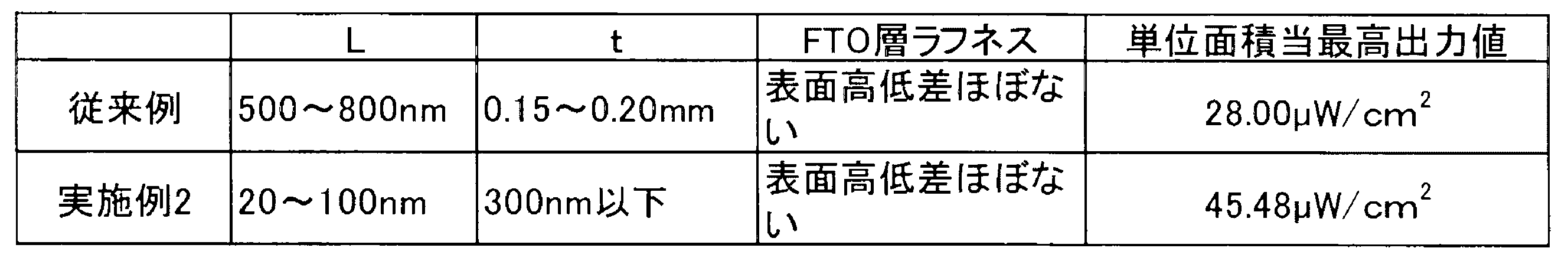
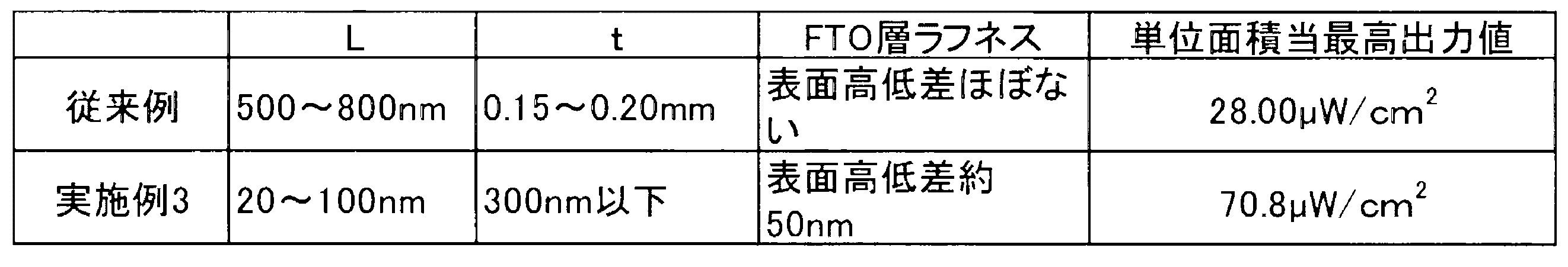
- a material having an average major axis L of 500 to 800 nm is used.
- the tandem photovoltaic device described here is characterized in that silicon dioxide is used as the photovoltaic layer. As shown in FIG. 9, it has been confirmed that silicon dioxide has a quantum efficiency higher than that of titanium dioxide in the ultraviolet region and absorbs light in the infrared region of 2500 nm or more. For this reason, compared with titanium dioxide, it has a photovoltaic effect in a wide wavelength region, and can realize extremely high power generation efficiency. With such a tandem photovoltaic device, the inventors of the present application have obtained a maximum output value of 28.00 ⁇ W / cm 2 per unit area at an illuminance of 1000 lux.
- Patent Document 1 and Patent Document 2 can be manufactured with a low-cost material compared to conventional solar cells, and the energy conversion efficiency is much higher than that of other photovoltaic elements. Very expensive. However, further improvements in energy conversion efficiency are required for photovoltaic devices.
- the photovoltaic layer of the photovoltaic element is composed of silicon dioxide fine particles having an average major axis of 100 nm or less.
- one of other typical photovoltaic elements is that the photovoltaic layer of the photovoltaic element is composed of silicon dioxide fine particles, and the thickness of the photovoltaic layer in the height direction is the average of the silicon dioxide fine particles. It is formed smaller than three times the major axis.
- the photovoltaic layer of the photovoltaic element is composed of silicon dioxide fine particles, and the silicon dioxide fine particles are formed as charge exchange layers having irregularities in the height direction. Is placed on top.
- corrugation of the height direction of a charge exchange layer is 50 nm or more, Preferably it is 100 nm or more.
- the photovoltaic device described above can greatly improve the power generation output per unit area as compared with a conventional photovoltaic device. Problems, configurations, and effects other than those described above will be clarified by the following embodiments.
- FIG. 1 is a cross-sectional view of a tandem photovoltaic device in Example 1.
- FIG. FIG. 2 is a cross-sectional view of a tandem photovoltaic device in Example 2.
- FIG. 3 is an enlarged view of a portion A in FIG. 4 is a cross-sectional view of a tandem photovoltaic device in Example 3.
- FIG. 5 is an enlarged view of a portion B in FIG.
- FIG. 6 is a schematic diagram showing the first conductive film in Example 3 in a bird's eye view.
- FIG. 7 is a cross-sectional view of a tandem photovoltaic device in a comparative example.
- FIG. 8 is a diagram showing an example of silicon dioxide fine particles.
- FIG. 9 is a measurement diagram of the quantum efficiency of a photovoltaic element including TiO 2 and a photovoltaic element including SiO 2 in the optical wavelength range.
- FIG. 1 is a cross-sectional view of a tandem photovoltaic device in Example 1
- FIG. 2 is a sectional view of a tandem photovoltaic device in Example 2
- FIG. 4 is a sectional view of a tandem photovoltaic device in Example 3.
- FIGS. 1, 2, and 4 since the following points are common to FIGS. 1, 2, and 4, they will be described with reference to FIG.
- the first substrate 12 and the second substrate 11 are tandem power generation elements using two photovoltaic layers, a first photovoltaic layer and a second photovoltaic layer.
- the second substrate on the light incident side is made of a transparent material, and preferably both are made of a transparent material.
- glass is generally used, but other than glass, resin such as plastic may be used.
- a transparent second conductive film 13 is formed on the second substrate.
- the second conductive film 13 is preferably FTO (fluorine-doped tin oxide), but may be, for example, indium-tin composite oxide (ITO) other than the FTO layer.
- FTO fluorine-doped tin oxide
- a second photovoltaic layer 16 is formed on the second conductive film 13.
- the second photovoltaic layer 16 is typically an oxide semiconductor layer, specifically, TiO 2 , SnO, ZnO, WO 3 , Nb 2 O 5 , In 2 O 3 , ZrO 2 , Ta 2.
- Oxide semiconductors such as O 5 and TiSrO 3 are preferable.
- a porous titanium dioxide layer solidified by sintering is more desirable.
- sulfide semiconductors such as CdS, ZnS, In 2 S, PbS, Mo 2 S, WS2, Sb 2 S3, Bi 2 S 3 , ZnCdS 2 , and CuS 2 may be used.
- metal chalcogenides such as CdSe, In 2 Se 2 , WSe 2 , PbSe, and CdTe are also applicable.
- elemental semiconductors such as GaAs, Si, Se, and InP may be used.
- a composite composed of two or more of the above-described substances such as a composite of SnO and ZnO and a composite of TiO 2 and Nb 2 O 5 can also be used.
- the kind of semiconductor is not limited to these, It can also use in mixture of 2 or more types.
- the layer thickness of the second photovoltaic layer 16 is preferably 3 to 30 ⁇ m in the height direction, and more preferably 6 to 20 ⁇ m.
- These second photovoltaic layers 16 can also carry a sensitizing dye.
- Various dyes can be applied as long as the dye supported on the second photovoltaic layer 16 exhibits a sensitizing action.
- N3 complex, N719 complex (N719 dye), Ru terpyridine complex (black dye), Ru diketonate Ru complexes such as complexes, organic dyes such as coumarin dyes, merocyanine dyes, and polyene dyes, metal porphyrin dyes, and phthalocyanine dyes are applicable.
- Ru complexes are preferable, and N719 dye and black dye are particularly preferable because they have a broad absorption spectrum in the visible light region.
- dyes may be used independently or can also be used in mixture of 2 or more types.
- a first conductive film (14 in FIGS. 1 and 2 and 22 in FIG. 4) is formed on the upper surface of the first substrate 12.
- the first conductive film is preferably FTO (fluorine-doped tin oxide), but may be, for example, indium-tin composite oxide (ITO) other than the FTO layer.
- FTO fluorine-doped tin oxide
- ITO indium-tin composite oxide
- a charge exchange layer (15 in FIGS. 1 and 2 and 23 in FIG. 4) is formed on the first conductive film.
- the charge exchange layer is preferably a platinum (Pt) film, but a carbon electrode, a conductive polymer, or the like can be used instead of the platinum (Pt) film.
- a first photovoltaic layer (21 in FIG. 1, 17 in FIG. 2, 24 in FIG. 4) is formed on the charge exchange layer.
- the first photovoltaic layer is formed on the charge exchange layer (15 in FIGS. 1 and 2; 23 in FIG. 4).
- the silicon dioxide fine particles 10 are dispersed as (21 in FIG. 1, 17 in FIG. 2, 24 in FIG. 4).
- the silicon dioxide fine particles 10 constituting the first photovoltaic layer are artificial quartz, fused silica glass, soda lime glass, alkali-free glass, Alternatively, glass particles made of borosilicate glass or the like are immersed in an aqueous solution of 5 to 10% hydrofluoric acid or hydrochloric acid, dried after washing with water, and then the major axis L of the particles is 20 to 100 nm. What was grind
- the electrolyte 19 is enclosed in the inside.
- the electrolyte 19 is used in a conventional dye-sensitized solar cell, and may be any of liquid, solid, solidified body, and room temperature molten salt.
- Examples of the electrolyte include a combination of metal iodide such as lithium iodide, sodium iodide, potassium iodide, and cesium iodide and iodine, and a fourth one such as tetraalkylammonium iodide, pyridinium iodide, and imidazolium iodide.
- metal iodide such as lithium iodide, sodium iodide, potassium iodide, and cesium iodide and iodine
- a fourth one such as tetraalkylammonium iodide, pyridinium iodide, and imidazolium iodide.
- the electrolyte When the electrolyte is an ionic liquid, it is not necessary to use a solvent.
- the electrolyte may be a gel electrolyte, a polymer electrolyte, or a solid electrolyte, and an organic charge transport material may be used instead of the electrolyte.
- Examples of the solvent when the electrolyte 19 is in the form of a solution include nitrile solvents such as acetonitrile, methoxyacetonitrile, and propionitrile, carbonate solvents such as ethylene carbonate, ether solvents, and the like.
- the electrolyte 19 used in Examples 1-3 specifically, 0.05 mol 0.1 mol, the I 2 and LiI, 4-tetra - butyl pyridine 0.5 mol, tetrabutylammonium iodide 0 .5 mol, added to acetonitrile solvent.
- the distance in the height direction between the first photovoltaic layer (21 in FIG. 1, 17 in FIG. 2, 24 in FIG. 4) and the second photovoltaic layer 16 is shorter. However, it is desirable to make it as short as possible because the movement of charges becomes easy.
- the thickness of the electrolyte portion 19 in the height direction, that is, the first photovoltaic layer (21 in FIG. 1, 17 in FIG. 2, 24 in FIG. 4) and the second light is 200 ⁇ m or less.
- the evaluation method of the maximum output value per unit area in this specification is as follows. Using a LED light (manufactured by Cosmo Techno Co., Ltd.), light is incident from the second substrate side, and light with a value of 1000 lux is irradiated to the photovoltaic device to be measured by a CEM illuminance meter DT-1309 did. Using a digital multimeter, the IV characteristics of the photovoltaic device to be measured were measured, and the values of short-circuit current, open-circuit voltage, and shape factor ff were obtained, and the maximum output value per unit area was derived.
- FIG. 1 is a diagram for explaining the first embodiment.
- the silicon dioxide fine particles 10 used for the first photovoltaic layer 21 have an average major axis L of 20 to 100 nm. These silicon dioxide fine particles 10 are dispersed so as to overlap on the flat first conductive film 14 (FTO layer) and the same flat charge exchange layer 15 (Pt layer) formed thereon, in the height direction.
- the first photovoltaic layer 21 having a thickness of 300 to 500 nm is formed.
- Other requirements and the like are as described as common items of the first to third embodiments.
- Example 1 the surface area of the silicon dioxide fine particles 10 in the first photovoltaic layer 21 is increased and the photovoltaic efficiency is increased by reducing the average major axis of the silicon dioxide fine particles 10 as compared with the conventional example. It is thought that.
- FIG. 2 is a diagram for explaining the second embodiment.
- the same materials and the like as in the first embodiment are used.
- the silicon dioxide fine particles 10 are formed on the flat first conductive film 14 and the same flat charge exchange layer 15 formed thereon so that the thickness in the height direction is 300 nm or less.
- a photovoltaic layer 17 is configured. That is, compared to Example 1, the thickness in the height direction of the first photovoltaic layer is reduced.
- FIG. 3 is an enlarged view of a portion A in FIG. 2.
- the silicon dioxide fine particles 10 constituting one photovoltaic layer 17 are dispersed in a state where there is little overlap between particles.
- Example 2 since the mobility of charges in the vicinity of the first photovoltaic layer 17 was improved by reducing the overlap of the silicon dioxide fine particles 10 in the first photovoltaic layer 17, the photovoltaic efficiency was increased. it is conceivable that. For this reason, in order to improve photovoltaic power generation efficiency, it is important not to spread the silicon dioxide fine particles 10 on the upper surface of the charge exchange layer 15 too much. That is, it can be confirmed that the amount of photovoltaic power generation is higher when the silicon dioxide fine particles 10 do not overlap each other and have a space.
- the thickness of the first photovoltaic layer 17 in the height direction is not more than three times the average major axis L of the silicon dioxide fine particles.
- the silicon dioxide fine particles 10 be disposed on the upper surface of the charge exchange layer 15 with a gap therebetween and dispersed. This is to prevent the conductivity between the charge exchange layer 15, the silicon dioxide fine particles 10 and the electrolyte 19 from being disturbed by arranging the silicon dioxide fine particles 10 in an overly dense manner.
- the charge exchange layer 15 and the silicon dioxide fine particles 10 and the electrolyte 19 are arranged with a margin, and the sum of the contact surface areas of the charge exchange layer 15 for performing charge exchange, the silicon dioxide fine particles 10 and the electrolyte 19 is the largest. It is desirable to be
- the first photovoltaic layer 17 has the silicon dioxide fine particles 10 to the extent that the charge exchange layer 15 can be seen from the gaps between the silicon dioxide fine particles 10 when the first substrate 12 is viewed from the second substrate 11 side.
- the amount of photovoltaic power generation can be increased by arranging.
- FIG. 4 is a diagram for explaining the third embodiment.
- the same materials as in the first and second embodiments are used.
- the first conductive film 22 (FTO layer) and the charge exchange layer 23 (Pt layer), which are the base on which the silicon dioxide fine particles 10 are disposed are not flat structures.
- the first conductive film 22 has irregularities (roughness, asperity) on the surface, and has a height difference of about 50 nm on the surface.
- the charge exchange layer 23 formed on the first conductive film 22 is also affected by the height difference of the first conductive film 22 and has irregularities on the surface.
- FIG. 5 is an enlarged view of part B in FIG.
- the silicon dioxide fine particles 10 constituting the first photovoltaic layer 24 are dispersed with little overlap on the first conductive film 22 having unevenness on the surface and the charge exchange layer 23 having the same unevenness formed thereon. is doing.
- the height difference of the irregularities on the surface of the first conductive film 22 is desirably 50 nm or more, and more desirably 100 nm or more. Further, the charge exchange layer 23 formed on the first conductive film 22 maintains the uneven shape on the surface of the first conductive film 22 without filling the unevenness on the surface of the first conductive film 22. It is desirable to be formed by.
- the arrangement of the silicon dioxide fine particles 10 dispersed on the charge exchange layer 23 formed on the first conductive film 22 is affected by the unevenness of the surfaces of the first conductive film 22 and the charge exchange layer 23 that are the underlying layers. receive. Combined with the uneven shape of the surface of the underlayer, the silicon dioxide fine particles 10 are arranged thinly dispersed. Thereby, it can be confirmed that the silicon dioxide fine particles 10 are not excessively overlapped and are disposed with an appropriate spatial margin, and the amount of photovoltaic power generation is increased.
- FIG. 6 is a schematic diagram showing the first conductive film 22 in a bird's eye view.
- the uneven shape on the surface of the first conductive film 22 not only the sharp shape as shown in FIG. 5 but also a structure 25 that is slightly rounded as shown in FIG. 6 exists. Also good. Furthermore, it is not necessary to have random unevenness as shown in FIGS. 5 and 6, and it may be an uneven shape in which cone shapes such as a three-dimensional cone, a triangular pyramid, and a quadrangular pyramid are regularly arranged.
- the present invention is not limited to the first to third embodiments, and various modifications can be made.
- the optimum average major axis of the silicon dioxide fine particles 10 can be changed according to the size distribution and shape distribution of the silicon dioxide fine particles 10 forming the first power generation layer.
- the optimum value of the thickness in the height direction of the first conductive film can also be changed according to the size distribution and shape distribution of the silicon dioxide fine particles 10.
- the height difference in the height direction of the unevenness of the first conductive film and / or the charge exchange layer, the shape of the unevenness, and the distribution of the unevenness in the direction parallel to the first substrate are the distribution of the size of the silicon dioxide fine particles 10.
- various optimum combinations are possible.
- other materials and configurations can be added, deleted, and replaced for a part of each embodiment.
Landscapes
- Engineering & Computer Science (AREA)
- Power Engineering (AREA)
- Microelectronics & Electronic Packaging (AREA)
- Chemical & Material Sciences (AREA)
- Chemical Kinetics & Catalysis (AREA)
- Electrochemistry (AREA)
- Life Sciences & Earth Sciences (AREA)
- Sustainable Development (AREA)
- Materials Engineering (AREA)
- General Chemical & Material Sciences (AREA)
- Photovoltaic Devices (AREA)
- Hybrid Cells (AREA)
Abstract
Description
図7を用いて、従来例として、二酸化ケイ素(SiO2)及び酸化チタン(TiO2)の二つの発電層を用いた、タンデム型発電素子を説明する。
光入射側のFTO層3の上には、焼結により固化された多孔質の二酸化チタン層6が形成されている。そして、多孔質の二酸化チタン層6には、ルテニウム錯体色素を吸着させたチタニア粒子を増感色素として担持させている。また、FTO層4の上には白金膜5が形成されている。
さらに、二酸化チタン層6と二酸化ケイ素層7の高さ方向の間隔は、0.2mm以上であり、四方を封止材8によって囲まれた中に電解質9が封入されている。
このように粉砕された二酸化ケイ素微粒子は、個々の形状は、球形に近いものもあるが図8に示すような非球体物も存在する。
上記した以外の課題、構成及び効果は、以下の実施形態により明らかにされる。
図1は、実施例1におけるタンデム型光発電素子の断面図、図2は、実施例2におけるタンデム型光発電素子の断面図、図4は、実施例3におけるタンデム型光発電素子の断面図であるが、以下の点は、図1、2、4において共通の事項であるので、代表的に図1を用いて説明する。
図1において、第一の基板12及び第二の基板11のうち、少なくとも光入射側となる第二の基板は透明材料で構成されており、好ましくは、双方とも透明材料で構成されている。透明材料としては、ガラスが一般的であるが、ガラス以外にもプラスチック等の樹脂でもよい。
第二の基板上には、透明な第二の導電膜13形成されている。第二の導電膜13は、好ましくはFTO(フッ素ドープ酸化錫)であるが、FTO層以外にも、例えば、インジウム-スズ複合酸化物(ITO)でもよい。
また、GaAs、Si、Se、InPなどの元素半導体などでもよい。
さらに、SnOとZnOとの複合体、TiO2とNb2O5の複合体などの、上述した物質の2種以上よりなる複合体を用いることもできる。
なお、半導体の種類はこれらに限定されるものでは無く、2種類以上混合して用いることもできる。
これらの第二の光発電層16の層厚は高さ方向で3~30μmであることが好ましく、より好ましくは6~20μmである。
また、これらの色素は単独で用いてもよいし、もしくは2種類以上を混合して用いることもできる。
第一の光発電層は、いずれも、実施例1~3のいずれの場合でも、電荷交換層(図1,2においては、15。図4においては23)の上に、第一の発電層 (図1においては21。図2においては、17。図4においては24)として、二酸化ケイ素微粒子10が分散されている。
実施例1~3においては、高さ方向の電解質19部分の厚み、すなわち第一の光発電層(図1においては21。図2においては、17。図4においては24)と第二の光発電層16との間の高さ方向の間隔は、200μm以下である。
LEDライト(株式会社コスモテクノ社製)を用いて、第二の基板側から光を入射させ、CEM社製照度計DT-1309で 1000luxの値となる光を測定対象となる光発電素子に照射した。デジタルマルチメーターを用いて、測定対象となる光発電素子のI-V特性を測定し、短絡電流、開放電圧、形状因子ffの値を得ると共に、単位面積当たりの最高出力値を導いた。
図1は実施例1を説明する図である。実施例1においては、第一の光発電層21に用いる二酸化ケイ素微粒子10として、平均長径Lが20~100nmのものを用いている。これらの二酸化ケイ素微粒子10が、平坦な第一の導電膜14(FTO層)とその上に形成された同じく平坦な電荷交換層15(Pt層)の上に重なり合うように分散され、高さ方向の厚さが300~500nmとなる第一の光発電層21を構成している。
他の要件等は、実施例1~3の共通事項として説明した通りである。

t:二酸化ケイ素層厚
図2は実施例2を説明する図である。実施例2においては、実施例1と同じ、材料等を用いている。しかし、二酸化ケイ素微粒子10を、平坦な第一の導電膜14とその上に形成された同じく平坦な電荷交換層15の上に、高さ方向の厚さが300nm以下となるように第一の光発電層17を構成している。
つまり、実施例1に比較して、第一の光発電層の高さ方向の厚みを小さくしている。
t:二酸化ケイ素層厚
このため、光発電効率を改善するためには、二酸化ケイ素微粒子10を電荷交換層15の上面に敷き詰め過ぎないことが重要である。つまり、二酸化ケイ素微粒子10が互いに重なり過ぎず、空間をもった状態である方が、光発電量が高くなることが確認できる。
図4は実施例3を説明する図である。実施例3においては、実施例1、2と同じ材料等を用いている。しかし、実施例3においては、二酸化ケイ素微粒子10を配置する下地となる、第一の導電膜22(FTO層)及び電荷交換層23(Pt層)が平坦な構造ではないものを採用している。図4に示すように、第一の導電膜22が表面に凹凸(roughness、asperity)を有しており、表面に約50nmの高低差を有している。
第一の導電膜22上に形成される電荷交換層23も、第一の導電膜22の高低差の影響を受け、表面に凹凸を有している。
t:二酸化ケイ素層厚
このような下地層の表面の凹凸の形状と相まって、二酸化ケイ素微粒子10は薄く分散して配置されることになる。これにより、二酸化ケイ素微粒子10は、過度に重ならず、適度な空間的な余裕を持って配置され、光発電量が高くなることが確認できる。
さらに、第一の導電膜及び/又は電荷交換層の凹凸の高さ方向の高低差や凹凸の形状、第一の基板と平行な方向における凹凸の分布は、二酸化ケイ素微粒子10の大きさの分布、形状の分布に応じて、様々な最適の組み合わせが可能である。
この他、各実施例の一部について他の材料や構成の追加、削除、置換をすることも可能であることは言うまでもない。
11・・・第二の基板
12・・・第一の基板
13・・・第二の導電膜
14・・・第一の導電膜
15・・・電荷交換層
16・・・第二の光発電層
17・・・第一の光発電層
18・・・封止材
19・・・電解質
21・・・第一の光発電層
22・・・第一の導電膜
23・・・電荷交換層
24・・・第一の光発電層
Claims (13)
- 第一の光発電層を有する光発電素子であって、
前記第一の光発電層が、平均長径が100nm以下の二酸化ケイ素微粒子によって構成されている光発電素子。 - 第一の光発電層を有する光発電素子であって、
前記第一の光発電層は、二酸化ケイ素微粒子によって構成されており、
前記第一の光発電層の高さ方向の厚さは、前記二酸化ケイ素微粒子の平均長径の3倍以下で形成されている光発電素子。 - 第一の光発電層を有する光発電素子であって、
前記第一の光発電層は、二酸化ケイ素微粒子によって構成されており、
前記二酸化ケイ素微粒子は、高さ方向に凹凸のある電荷交換層の上に配置されている光発電素子。 - 第一の光発電層を有する光発電素子であって、
前記第一の光発電層は、二酸化ケイ素微粒子によって構成されており、
前記二酸化ケイ素微粒子は、高さ方向に凹凸のある第一導電膜の上面に形成され、高さ方向に凹凸のある電荷交換層上に配置されている光発電素子。 - 請求項3において、
前記電荷交換層の高さ方向の凹凸は、50nm以上である光発電素子。 - 請求項4において、
前記第一導電膜の高さ方向の凹凸は、50nm以上である光発電素子。 - 第一の導電膜を一方の表面に有する第一の基板と第二の導電膜を一方の表面に有する第二の基板が、第一の導電膜及び第二の導電膜が互いに向かい合って配置されており、
前記第二の導電膜の上に、第二の光発電層が配置されており、
前記第一の導電膜の上に、電荷交換層が配置されており、
前記電荷交換層の上に、第一の光発電層が配置されており、
前記第二の光発電層と前記第一の光発電層と間に、電解液が配置されており、
前記第一の光発電層は、平均長径が100nm以下の二酸化ケイ素微粒子によって構成されている光発電素子。 - 請求項7において、
前記第一の光発電層は、高さ方向の厚さが、前記二酸化ケイ素微粒子の平均長径の3倍以下となるように、二酸化ケイ素微粒子が配置されている光発電素子。 - 請求項7において、
前記第一の光発電層は、第二の基板側から第一の基盤を見た場合に、二酸化ケイ素微粒子の隙間から、前記電荷交換層が見える程度に、前記二酸化ケイ素微粒子が配置された光発電素子。 - 請求項7から9のいずれか一項において、
前記電荷交換層、及び/又は、前記第一の導電膜は、高さ方向に50nm以上の凹凸を有する光発電素子。 - 請求項1から10のいずれか一項において、
前記二酸化ケイ素微粒子は、ハロゲン化水素酸に浸漬処理された二酸化ケイ素である光発電素子。 - 請求項7から11のいずれか一項において、
前記第二の発電層は、TiO2、SnO、ZnO、WO3、Nb2O5、In2O3、ZrO2、Ta2O5、TiSrO3から選ばれた物質である光発電素子。 - 請求項7から12のいずれか一項において、前記第二の発電層は、増感色素を担持させたものである光発電素子。
Priority Applications (12)
| Application Number | Priority Date | Filing Date | Title |
|---|---|---|---|
| AU2016385211A AU2016385211B2 (en) | 2016-01-06 | 2016-12-27 | Photovoltaic element |
| PL16883856T PL3401938T3 (pl) | 2016-01-06 | 2016-12-27 | Element fotowoltaiczny |
| EP20191884.4A EP3758032B1 (en) | 2016-01-06 | 2016-12-27 | Photovoltaic element |
| DK16883856.3T DK3401938T3 (da) | 2016-01-06 | 2016-12-27 | Fotovoltaisk element |
| RU2018127840A RU2703519C1 (ru) | 2016-01-06 | 2016-12-27 | Фотоэлектрический элемент |
| US16/067,988 US20190006121A1 (en) | 2016-01-06 | 2016-12-27 | Photovoltaic element |
| EP16883856.3A EP3401938B1 (en) | 2016-01-06 | 2016-12-27 | Photovoltaic element |
| CN201680077860.2A CN108475582B (zh) | 2016-01-06 | 2016-12-27 | 光发电元件 |
| ES16883856T ES2910044T3 (es) | 2016-01-06 | 2016-12-27 | Elemento fotovoltaico |
| PH12018501441A PH12018501441A1 (en) | 2016-01-06 | 2018-07-05 | Photovoltaic element |
| AU2019219769A AU2019219769B2 (en) | 2016-01-06 | 2019-08-21 | Photovoltaic element |
| US16/861,398 US20200279694A1 (en) | 2016-01-06 | 2020-04-29 | Photovoltaic element |
Applications Claiming Priority (2)
| Application Number | Priority Date | Filing Date | Title |
|---|---|---|---|
| JP2016-001278 | 2016-01-06 | ||
| JP2016001278A JP6773944B2 (ja) | 2016-01-06 | 2016-01-06 | 光発電素子 |
Related Child Applications (2)
| Application Number | Title | Priority Date | Filing Date |
|---|---|---|---|
| US16/067,988 A-371-Of-International US20190006121A1 (en) | 2016-01-06 | 2016-12-27 | Photovoltaic element |
| US16/861,398 Division US20200279694A1 (en) | 2016-01-06 | 2020-04-29 | Photovoltaic element |
Publications (1)
| Publication Number | Publication Date |
|---|---|
| WO2017119357A1 true WO2017119357A1 (ja) | 2017-07-13 |
Family
ID=59274092
Family Applications (1)
| Application Number | Title | Priority Date | Filing Date |
|---|---|---|---|
| PCT/JP2016/088848 Ceased WO2017119357A1 (ja) | 2016-01-06 | 2016-12-27 | 光発電素子 |
Country Status (13)
| Country | Link |
|---|---|
| US (2) | US20190006121A1 (ja) |
| EP (2) | EP3401938B1 (ja) |
| JP (1) | JP6773944B2 (ja) |
| CN (2) | CN108475582B (ja) |
| AU (2) | AU2016385211B2 (ja) |
| DK (2) | DK3758032T3 (ja) |
| ES (2) | ES3030687T3 (ja) |
| FI (1) | FI3758032T3 (ja) |
| PH (1) | PH12018501441A1 (ja) |
| PL (2) | PL3401938T3 (ja) |
| RU (1) | RU2703519C1 (ja) |
| TW (1) | TWI708274B (ja) |
| WO (1) | WO2017119357A1 (ja) |
Families Citing this family (2)
| Publication number | Priority date | Publication date | Assignee | Title |
|---|---|---|---|---|
| JP2019021767A (ja) * | 2017-07-18 | 2019-02-07 | 国際先端技術総合研究所株式会社 | 光発電素子及びその製造方法 |
| RU196426U1 (ru) * | 2019-12-27 | 2020-02-28 | федеральное государственное автономное образовательное учреждение высшего образования "Национальный исследовательский университет ИТМО" (Университет ИТМО) | Прозрачный гетеропереход на основе оксидов |
Citations (3)
| Publication number | Priority date | Publication date | Assignee | Title |
|---|---|---|---|---|
| WO2012124656A1 (ja) * | 2011-03-11 | 2012-09-20 | 国際先端技術総合研究所株式会社 | 2酸化ケイ素ソーラーセル |
| JP2012234693A (ja) * | 2011-04-28 | 2012-11-29 | International Frontier Technology Laboratory Inc | ソーラーセル |
| JP2013161775A (ja) * | 2012-02-09 | 2013-08-19 | Peccell Technologies Inc | 色素増感型光電変換素子およびそれを用いた色素増感型太陽電池の製造方法 |
Family Cites Families (26)
| Publication number | Priority date | Publication date | Assignee | Title |
|---|---|---|---|---|
| JPH11317538A (ja) * | 1998-02-17 | 1999-11-16 | Canon Inc | 光導電性薄膜および光起電力素子 |
| FR2800731B1 (fr) * | 1999-11-05 | 2002-01-18 | Saint Gobain Vitrage | Substrat transparent muni d'une couche en derive de silicium |
| EP1180774B1 (en) * | 2000-08-15 | 2006-10-11 | Fuji Photo Film Co., Ltd. | Photoelectric conversion device and method for producing same |
| JP2005111218A (ja) * | 2003-10-07 | 2005-04-28 | Rabaa:Kk | 衣類収納洗濯ネット |
| WO2005078853A1 (ja) * | 2004-02-13 | 2005-08-25 | Bridgestone Corporation | 色素増感型太陽電池 |
| JP4863662B2 (ja) * | 2005-07-06 | 2012-01-25 | シャープ株式会社 | 色素増感型太陽電池モジュールおよびその製造方法 |
| JP4856079B2 (ja) * | 2005-09-02 | 2012-01-18 | 京セラ株式会社 | 光電変換装置及びその製造方法並びに光発電装置 |
| WO2007043533A1 (ja) * | 2005-10-11 | 2007-04-19 | Kyocera Corporation | 光電変換装置及びその製造方法並びに光発電装置 |
| KR100728194B1 (ko) * | 2005-11-11 | 2007-06-13 | 삼성에스디아이 주식회사 | 염료 감응형 태양 전지 및 이의 제조 방법 |
| US7902072B2 (en) * | 2006-02-28 | 2011-03-08 | Fujifilm Corporation | Metal-polishing composition and chemical-mechanical polishing method |
| EP1936644A3 (en) * | 2006-12-22 | 2011-01-05 | Sony Deutschland Gmbh | A photovoltaic cell |
| JP2008257893A (ja) * | 2007-03-30 | 2008-10-23 | Dainippon Printing Co Ltd | 色素増感型太陽電池用基板の製造方法、色素増感型太陽電池の製造方法、および、これらによって製造された色素増感型太陽電池用基板および色素増感型太陽電池。 |
| CN102027556B (zh) * | 2008-04-18 | 2013-04-17 | Nlab太阳能股份公司 | 太阳能向电能转化的装置 |
| CN101620938B (zh) * | 2008-07-05 | 2011-12-14 | 比亚迪股份有限公司 | 一种半导体电极及制法和含有该半导体电极的太阳能电池 |
| WO2010046180A2 (en) * | 2008-10-22 | 2010-04-29 | Applied Materials Inc. - A Corporation Of The State Of Delaware | Semiconductor device and method of producing a semiconductor device |
| JP5422645B2 (ja) * | 2009-04-15 | 2014-02-19 | シャープ株式会社 | 色素増感太陽電池および色素増感太陽電池モジュール |
| CN101866963B (zh) * | 2009-07-20 | 2012-12-26 | 湖南共创光伏科技有限公司 | 高转化率硅基多结多叠层pin薄膜太阳能电池及其制造方法 |
| AU2010308884A1 (en) | 2009-10-21 | 2012-05-10 | International Frontier Technology Laboratory, Inc. | Photoelectrode material and photocell material |
| US9224892B2 (en) * | 2009-12-21 | 2015-12-29 | Ppg Industries Ohio, Inc. | Silicon thin film solar cell having improved haze and methods of making the same |
| KR101135476B1 (ko) * | 2010-11-16 | 2012-04-13 | 삼성에스디아이 주식회사 | 염료 감응 태양 전지 |
| JP5118233B2 (ja) * | 2011-06-08 | 2013-01-16 | シャープ株式会社 | 光電変換素子および光電変換素子モジュール |
| CN102543468A (zh) * | 2012-01-04 | 2012-07-04 | 复旦大学 | 以取向碳纳米管薄膜为对电极的染料敏化太阳能电池 |
| CN102751105B (zh) * | 2012-06-26 | 2015-07-15 | 北京交通大学 | 一种染料敏化太阳能电池光阳极的制备方法 |
| JP2014095099A (ja) * | 2012-11-07 | 2014-05-22 | Sumitomo Metal Mining Co Ltd | 透明導電膜積層体及びその製造方法、並びに薄膜太陽電池及びその製造方法 |
| JP6235235B2 (ja) * | 2013-05-10 | 2017-11-22 | 三愛工業株式会社 | 洗濯ネット袋 |
| JP6121971B2 (ja) * | 2014-10-17 | 2017-04-26 | 松本ナ−ス産業株式会社 | 洗濯用ネット |
-
2016
- 2016-01-06 JP JP2016001278A patent/JP6773944B2/ja active Active
- 2016-12-27 DK DK20191884.4T patent/DK3758032T3/da active
- 2016-12-27 ES ES20191884T patent/ES3030687T3/es active Active
- 2016-12-27 PL PL16883856T patent/PL3401938T3/pl unknown
- 2016-12-27 PL PL20191884.4T patent/PL3758032T3/pl unknown
- 2016-12-27 DK DK16883856.3T patent/DK3401938T3/da active
- 2016-12-27 AU AU2016385211A patent/AU2016385211B2/en active Active
- 2016-12-27 RU RU2018127840A patent/RU2703519C1/ru active
- 2016-12-27 ES ES16883856T patent/ES2910044T3/es active Active
- 2016-12-27 CN CN201680077860.2A patent/CN108475582B/zh active Active
- 2016-12-27 US US16/067,988 patent/US20190006121A1/en not_active Abandoned
- 2016-12-27 EP EP16883856.3A patent/EP3401938B1/en active Active
- 2016-12-27 EP EP20191884.4A patent/EP3758032B1/en active Active
- 2016-12-27 CN CN202010156599.3A patent/CN111508715A/zh active Pending
- 2016-12-27 FI FIEP20191884.4T patent/FI3758032T3/fi active
- 2016-12-27 WO PCT/JP2016/088848 patent/WO2017119357A1/ja not_active Ceased
- 2016-12-29 TW TW105143927A patent/TWI708274B/zh active
-
2018
- 2018-07-05 PH PH12018501441A patent/PH12018501441A1/en unknown
-
2019
- 2019-08-21 AU AU2019219769A patent/AU2019219769B2/en active Active
-
2020
- 2020-04-29 US US16/861,398 patent/US20200279694A1/en not_active Abandoned
Patent Citations (3)
| Publication number | Priority date | Publication date | Assignee | Title |
|---|---|---|---|---|
| WO2012124656A1 (ja) * | 2011-03-11 | 2012-09-20 | 国際先端技術総合研究所株式会社 | 2酸化ケイ素ソーラーセル |
| JP2012234693A (ja) * | 2011-04-28 | 2012-11-29 | International Frontier Technology Laboratory Inc | ソーラーセル |
| JP2013161775A (ja) * | 2012-02-09 | 2013-08-19 | Peccell Technologies Inc | 色素増感型光電変換素子およびそれを用いた色素増感型太陽電池の製造方法 |
Non-Patent Citations (1)
| Title |
|---|
| See also references of EP3401938A4 * |
Also Published As
| Publication number | Publication date |
|---|---|
| CN111508715A (zh) | 2020-08-07 |
| EP3758032A1 (en) | 2020-12-30 |
| PH12018501441A1 (en) | 2019-03-04 |
| AU2016385211B2 (en) | 2019-10-03 |
| AU2019219769B2 (en) | 2021-01-21 |
| CN108475582B (zh) | 2021-02-23 |
| PL3758032T3 (pl) | 2025-07-28 |
| US20190006121A1 (en) | 2019-01-03 |
| EP3401938B1 (en) | 2022-01-19 |
| DK3758032T3 (da) | 2025-05-19 |
| TW201801109A (zh) | 2018-01-01 |
| PL3401938T3 (pl) | 2022-05-23 |
| ES2910044T3 (es) | 2022-05-11 |
| AU2016385211A1 (en) | 2018-07-26 |
| EP3758032B1 (en) | 2025-05-14 |
| JP6773944B2 (ja) | 2020-10-21 |
| DK3401938T3 (da) | 2022-03-28 |
| EP3401938A4 (en) | 2020-01-08 |
| TWI708274B (zh) | 2020-10-21 |
| JP2017123392A (ja) | 2017-07-13 |
| RU2703519C1 (ru) | 2019-10-18 |
| FI3758032T3 (fi) | 2025-07-08 |
| EP3401938A1 (en) | 2018-11-14 |
| CN108475582A (zh) | 2018-08-31 |
| US20200279694A1 (en) | 2020-09-03 |
| ES3030687T3 (en) | 2025-07-01 |
| AU2019219769A1 (en) | 2019-09-05 |
Similar Documents
| Publication | Publication Date | Title |
|---|---|---|
| Bhandari et al. | Performance of WO3-incorporated carbon electrodes for ambient mesoscopic perovskite solar cells | |
| Kim et al. | Highly durable and efficient quantum dot-sensitized solar cells based on oligomer gel electrolytes | |
| JP6165054B2 (ja) | 光起電素子 | |
| Nguyen et al. | 3-D solar cells by electrochemical-deposited Se layer as extremely-thin absorber and hole conducting layer on nanocrystalline TiO2 electrode | |
| Li et al. | Preparation of SnS quantum dots for solar cells application by an in-situ solution chemical reaction process | |
| Bhambhani | Quantum dot-sensitized solar cells: a review | |
| AU2019219769B2 (en) | Photovoltaic element | |
| US20130042906A1 (en) | Quantum-dot sensitized solar cell | |
| US20110155233A1 (en) | Hybrid solar cells | |
| CN103426645B (zh) | 利用双面涂覆的金属基板的金属柔性染料敏化太阳能电池及其制造方法 | |
| KR101465360B1 (ko) | 태양전지용 광전극 및 이를 포함한 태양전지 | |
| JP6670430B2 (ja) | 光発電素子及び光発電素子の製造方法 | |
| JP5376850B2 (ja) | 広帯域波長領域の光電変換を可能にする太陽電池 | |
| HK40000196A (en) | Photovoltaic element | |
| JP7410520B2 (ja) | ハイブリッド強誘電性ディスコティック液晶太陽電池 | |
| Arof et al. | Plasmonic effect in photoelectrochemical cells | |
| Borysiewicz et al. | Dye aggregation influence on dye sensitized solar cell performance in nanocoral ZnO-based thin film cells sensitized with N-719 and rose bengal dyes | |
| TW201427049A (zh) | 具硫化鉛相對電極之量子點敏化太陽能電池及其製造方法 | |
| Musa et al. | Dye Sensitized Solar Cells Incorporated with Tio2-ZnO Nanoparticles | |
| TWM486145U (zh) | 染料敏化太陽能電池 | |
| CN102347144A (zh) | 具有针状电极的光化学太阳能电池及其制造方法 | |
| Kolay | Study of TiO2 Morphologies for CdS Quantum Dots Sensitized Solar Cells | |
| Pang et al. | Study on the origin of the open-circuit photovoltage enhancement in TiO2 nanotube-based dye sensitised solar cells |
Legal Events
| Date | Code | Title | Description |
|---|---|---|---|
| 121 | Ep: the epo has been informed by wipo that ep was designated in this application |
Ref document number: 16883856 Country of ref document: EP Kind code of ref document: A1 |
|
| WWE | Wipo information: entry into national phase |
Ref document number: 12018501441 Country of ref document: PH |
|
| NENP | Non-entry into the national phase |
Ref country code: DE |
|
| ENP | Entry into the national phase |
Ref document number: 2016385211 Country of ref document: AU Date of ref document: 20161227 Kind code of ref document: A |
|
| WWE | Wipo information: entry into national phase |
Ref document number: 2016883856 Country of ref document: EP |
|
| ENP | Entry into the national phase |
Ref document number: 2016883856 Country of ref document: EP Effective date: 20180806 |
|
| WWE | Wipo information: entry into national phase |
Ref document number: 12024551937 Country of ref document: PH |