WO2017122436A1 - 固体撮像装置 - Google Patents
固体撮像装置 Download PDFInfo
- Publication number
- WO2017122436A1 WO2017122436A1 PCT/JP2016/085074 JP2016085074W WO2017122436A1 WO 2017122436 A1 WO2017122436 A1 WO 2017122436A1 JP 2016085074 W JP2016085074 W JP 2016085074W WO 2017122436 A1 WO2017122436 A1 WO 2017122436A1
- Authority
- WO
- WIPO (PCT)
- Prior art keywords
- light receiving
- receiving unit
- deep
- shallow
- solid
- Prior art date
- Legal status (The legal status is an assumption and is not a legal conclusion. Google has not performed a legal analysis and makes no representation as to the accuracy of the status listed.)
- Ceased
Links
Images


Classifications
-
- H—ELECTRICITY
- H04—ELECTRIC COMMUNICATION TECHNIQUE
- H04N—PICTORIAL COMMUNICATION, e.g. TELEVISION
- H04N25/00—Circuitry of solid-state image sensors [SSIS]; Control thereof
- H04N25/60—Noise processing, e.g. detecting, correcting, reducing or removing noise
- H04N25/62—Detection or reduction of noise due to excess charges produced by the exposure, e.g. smear, blooming, ghost image, crosstalk or leakage between pixels
-
- H—ELECTRICITY
- H04—ELECTRIC COMMUNICATION TECHNIQUE
- H04N—PICTORIAL COMMUNICATION, e.g. TELEVISION
- H04N25/00—Circuitry of solid-state image sensors [SSIS]; Control thereof
- H04N25/70—SSIS architectures; Circuits associated therewith
-
- H—ELECTRICITY
- H04—ELECTRIC COMMUNICATION TECHNIQUE
- H04N—PICTORIAL COMMUNICATION, e.g. TELEVISION
- H04N25/00—Circuitry of solid-state image sensors [SSIS]; Control thereof
- H04N25/70—SSIS architectures; Circuits associated therewith
- H04N25/76—Addressed sensors, e.g. MOS or CMOS sensors
-
- H—ELECTRICITY
- H10—SEMICONDUCTOR DEVICES; ELECTRIC SOLID-STATE DEVICES NOT OTHERWISE PROVIDED FOR
- H10F—INORGANIC SEMICONDUCTOR DEVICES SENSITIVE TO INFRARED RADIATION, LIGHT, ELECTROMAGNETIC RADIATION OF SHORTER WAVELENGTH OR CORPUSCULAR RADIATION
- H10F30/00—Individual radiation-sensitive semiconductor devices in which radiation controls the flow of current through the devices, e.g. photodetectors
- H10F30/20—Individual radiation-sensitive semiconductor devices in which radiation controls the flow of current through the devices, e.g. photodetectors the devices having potential barriers, e.g. phototransistors
-
- H—ELECTRICITY
- H10—SEMICONDUCTOR DEVICES; ELECTRIC SOLID-STATE DEVICES NOT OTHERWISE PROVIDED FOR
- H10F—INORGANIC SEMICONDUCTOR DEVICES SENSITIVE TO INFRARED RADIATION, LIGHT, ELECTROMAGNETIC RADIATION OF SHORTER WAVELENGTH OR CORPUSCULAR RADIATION
- H10F39/00—Integrated devices, or assemblies of multiple devices, comprising at least one element covered by group H10F30/00, e.g. radiation detectors comprising photodiode arrays
- H10F39/10—Integrated devices
- H10F39/12—Image sensors
- H10F39/18—Complementary metal-oxide-semiconductor [CMOS] image sensors; Photodiode array image sensors
- H10F39/182—Colour image sensors
- H10F39/1825—Multicolour image sensors having stacked structure, e.g. NPN, NPNPN or multiple quantum well [MQW] structures
-
- H—ELECTRICITY
- H10—SEMICONDUCTOR DEVICES; ELECTRIC SOLID-STATE DEVICES NOT OTHERWISE PROVIDED FOR
- H10F—INORGANIC SEMICONDUCTOR DEVICES SENSITIVE TO INFRARED RADIATION, LIGHT, ELECTROMAGNETIC RADIATION OF SHORTER WAVELENGTH OR CORPUSCULAR RADIATION
- H10F39/00—Integrated devices, or assemblies of multiple devices, comprising at least one element covered by group H10F30/00, e.g. radiation detectors comprising photodiode arrays
- H10F39/10—Integrated devices
- H10F39/12—Image sensors
- H10F39/18—Complementary metal-oxide-semiconductor [CMOS] image sensors; Photodiode array image sensors
- H10F39/184—Infrared image sensors
- H10F39/1847—Multispectral infrared image sensors having a stacked structure, e.g. NPN, NPNPN or multiple quantum well [MQW] structures
-
- H—ELECTRICITY
- H10—SEMICONDUCTOR DEVICES; ELECTRIC SOLID-STATE DEVICES NOT OTHERWISE PROVIDED FOR
- H10F—INORGANIC SEMICONDUCTOR DEVICES SENSITIVE TO INFRARED RADIATION, LIGHT, ELECTROMAGNETIC RADIATION OF SHORTER WAVELENGTH OR CORPUSCULAR RADIATION
- H10F39/00—Integrated devices, or assemblies of multiple devices, comprising at least one element covered by group H10F30/00, e.g. radiation detectors comprising photodiode arrays
- H10F39/10—Integrated devices
- H10F39/12—Image sensors
- H10F39/18—Complementary metal-oxide-semiconductor [CMOS] image sensors; Photodiode array image sensors
- H10F39/186—Complementary metal-oxide-semiconductor [CMOS] image sensors; Photodiode array image sensors having arrangements for blooming suppression
- H10F39/1865—Overflow drain structures
-
- H—ELECTRICITY
- H10—SEMICONDUCTOR DEVICES; ELECTRIC SOLID-STATE DEVICES NOT OTHERWISE PROVIDED FOR
- H10F—INORGANIC SEMICONDUCTOR DEVICES SENSITIVE TO INFRARED RADIATION, LIGHT, ELECTROMAGNETIC RADIATION OF SHORTER WAVELENGTH OR CORPUSCULAR RADIATION
- H10F39/00—Integrated devices, or assemblies of multiple devices, comprising at least one element covered by group H10F30/00, e.g. radiation detectors comprising photodiode arrays
- H10F39/011—Manufacture or treatment of image sensors covered by group H10F39/12
Definitions
- the present invention relates to a solid-state imaging device used as a two-dimensional image sensor or the like.
- Patent Document 1 shows that a photodiode that performs photoelectric conversion of infrared light is extended to a lower portion of the photodiode that performs photoelectric conversion of visible light, thereby improving infrared sensitivity.
- the drain part for discharging excess charges generated in the visible light receiving part is provided on the substrate surface. It is necessary to form on the side. As a result, the light receiving portion becomes narrow, and the saturation output and sensitivity are lowered.
- an object of the present invention is to obtain a good image quality in which color mixing, saturation output, and sensitivity reduction are suppressed even when the infrared light receiving unit is extended under the visible light receiving unit.
- An imaging device is provided.
- the solid-state imaging device of the present disclosure has a plurality of pixels arranged two-dimensionally on a semiconductor substrate.
- Each of the plurality of pixels includes at least one shallow light receiving portion formed near the surface of the semiconductor substrate and at least one deep light receiving portion formed below the shallow light receiving portion.
- a part of the shallow light receiving part and the deep light receiving part are connected to form a second light receiving part, and the other shallow light receiving part constitutes the first light receiving part. Excess charge in the first light receiving part is discharged to the deep light receiving part.
- the solid-state imaging device of the present disclosure by discharging excess charge in the first light receiving unit to the deep light receiving unit, it is not necessary to provide a drain unit for discharging the excess charge on the substrate surface side. Yes. As a result, a good image can be obtained without narrowing the light receiving section and appropriately discharging excess charges to suppress color mixing.
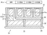
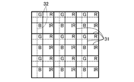
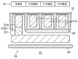
- FIG. 1 is a plan view schematically illustrating a two-dimensional array of pixels and light receiving units in an exemplary solid-state imaging device of the present disclosure.
- FIG. 2 is a diagram schematically showing a cross section taken along line II-II ′ of the solid-state imaging device of FIG.
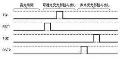
- FIG. 3 is an equivalent circuit diagram of an exemplary solid-state imaging device.
- FIG. 4 is a diagram illustrating an example of a driving method during imaging of the exemplary solid-state imaging device.
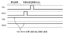
- FIG. 5 is a diagram illustrating an example of a more preferable driving method during imaging of the exemplary solid-state imaging device.
- FIG. 6 is a diagram illustrating an example of a more preferable driving method during imaging of the exemplary solid-state imaging device.
- FIG. 1 is a plan view schematically illustrating a two-dimensional array of pixels and light receiving units in an exemplary solid-state imaging device of the present disclosure.
- FIG. 2 is a diagram schematically showing a cross section taken along line II-II ′
- FIG. 7 is a diagram illustrating a modification example regarding the color filter of the solid-state imaging device of the present disclosure.
- FIG. 8 is a diagram illustrating a modification example regarding the color filter of the solid-state imaging device of the present disclosure.
- FIG. 9 is a diagram illustrating a modification example regarding the pixel arrangement in the solid-state imaging device of the present disclosure.
- FIG. 10 is a diagram illustrating a modification example of the solid-state imaging device of the present disclosure.
- FIG. 11 is a plan view schematically showing the arrangement of the light receiving unit and the readout circuit unit in the solid-state imaging device of the present disclosure.
- FIG. 12 is a plan view schematically showing that a conventional solid-state imaging device includes a drain portion in addition to a light receiving portion and a readout circuit portion.
- FIGS. 1 and 2 are schematic diagrams showing the configuration of an exemplary solid-state imaging device 50.
- FIG. FIG. 1 is a plan view showing an arrangement of pixels and light receiving portions of the solid-state imaging device 50
- FIG. 2 is a cross-sectional view showing a cross-sectional configuration taken along line II-II ′ of FIG.
- a plurality of pixels are two-dimensionally arranged on a semiconductor substrate such as silicon, and each pixel has red (R), green (G) and blue (B) visible light and infrared light.
- the light receiving units having color filters corresponding to the four colors (IR) are arranged in a 2 ⁇ 2 array.
- the color filters corresponding to R, G, and B transmit visible light and infrared light of each color, and the IR filter transmits only infrared light.
- the solid-state imaging device 50 includes a shallow light-receiving unit 11 (11 a and 11 b) formed in the vicinity of the surface of the semiconductor substrate 71, and a deep light-receiving unit 12 formed therebelow. .
- the deep layer light receiving unit 12 extends below the 2 ⁇ 2 four shallow layer light receiving units 11 included in one pixel and is connected to the shallow layer by the connection unit 21.
- the second light receiving unit 13 is configured by being connected to a part (11b) of the light receiving unit.
- An IR filter is provided above the shallow-layer light-receiving unit 11b that constitutes the second light-receiving unit 13.
- the other shallow light-receiving parts 11a that do not constitute the second light-receiving part 13 are each provided with one of the visible light filters, and constitute a first light-receiving part that receives light of the corresponding color.
- a part of the light can be absorbed if infrared light is incident.
- a part can be absorbed.
- a shallow horizontal separation part 31 is provided between the shallow light receiving parts 11.
- the shallow light receiving unit 11 is two-dimensionally arranged via the shallow horizontal separating unit 31.
- a deep horizontal separation portion 32 is provided between the deep light receiving portions 12.
- the deep light receiving unit 12 is two-dimensionally arranged via the deep horizontal separation unit 32.
- a vertical separation unit 33 is provided between the shallow light receiving unit 11 and the deep light receiving unit 12. The light receiving parts are separated from each other by these separating parts.
- a vertical overflow barrier 34 that separates the deep light-receiving part 12 from the semiconductor substrate 71 in the lower part is provided below the deep light-receiving part 12.
- the above shallow layer light receiving unit 11 (11a and 11b), deep layer light receiving unit 12, connection unit 21, shallow layer horizontal separation unit 31, deep layer horizontal separation unit 32, vertical separation unit 33, and vertical overflow barrier 34 are all, for example, It is formed by introducing impurities into the semiconductor substrate 71.
- the potential barrier of the vertical separation unit 33 is set to be smaller than the potential barrier of the shallow horizontal separation unit 31.
- the potential (potential) in the vertical separation unit 33 is made higher than the potential in the shallow horizontal separation unit 31.
- FIG. 11 and FIG. 12 shows a conventional solid-state imaging device in which a second light receiving unit is provided below the first light receiving unit, one light receiving unit 61, a readout circuit unit 62 for reading a signal from the light receiving unit 61, and a light receiving unit.
- 6 is a plan view schematically showing a relationship with a drain part 63 for discharging excess charges generated in the part 61.
- FIG. In the conventional solid-state imaging device, it is necessary to provide the drain part 63 on the surface side of the semiconductor substrate 71, and the area where the light receiving part 61 can be provided is reduced by the area occupied by the drain part 63. As a result, the saturation output is lowered, the light path is narrowed, the light that can be received is reduced, and the sensitivity is lowered.
- FIG. 11 includes one light receiving unit 61 and a readout circuit unit 62 for reading a signal from the light receiving unit 61
- the drain unit 63 includes the exemplary solid-state imaging device 50 of the present application. It is a top view which shows not. This is realized by eliminating the excessive charge in the shallow light-receiving part 11a of FIG. 2 to the deep light-receiving part 12, so that it is not necessary to provide the drain part 63 on the surface side of the semiconductor substrate 71. As a result, in the configuration of FIG. 12, the area of the light receiving unit 61 can be increased compared to the configuration of FIG. 11, and the sensitivity can be improved.
- the potential barriers of the vertical separation unit 33 and the vertical overflow barrier 34 of the solid-state imaging device 50 are both smaller than the potential barrier of the deep horizontal separation unit 32 (if the charge carriers are electrons, the potential is increased). May be. Thereby, when acquiring an infrared image, excess charges generated in the deep light receiving unit 12 are discharged to the shallow light receiving unit 11 a side or the semiconductor substrate 71 side below the vertical overflow barrier 34. That is, excessive charges leak out in the horizontal direction (to the adjacent deep light receiving unit 12) and color mixing is suppressed, and a good infrared image can be acquired. Also in this case, as shown in FIGS. 11 and 12, it is unnecessary to provide a drain portion for discharging excess charges on the surface side of the semiconductor substrate 71, and the effect of improving the saturation output and sensitivity can be obtained. can get.
- the potential barrier of the vertical overflow barrier 34 may be made smaller than the potential barrier of the vertical separation unit 33 (if the charge carriers are electrons, the potential is increased). In this case, excess charges generated in the deep light receiving unit 12 are discharged to the semiconductor substrate 71 below the vertical overflow barrier 34.
- FIG. 3 is an equivalent circuit diagram of the exemplary solid-state imaging device 50.
- the shallow light-receiving unit 11 a first light-receiving unit
- the second light-receiving unit 13 a vertical separation unit 33 that separates them
- the second light-receiving unit 13 and the semiconductor substrate therebelow are separated.
- a separating vertical overflow barrier 34 is shown.
- transfer gates TG1 and TG2 for reading signals from the shallow light receiving unit 11a and the second light receiving unit 13 and a readout circuit connected to them are shown.
- the shallow layer light receiving unit 11a or the second light receiving unit 13 When light enters the shallow layer light receiving unit 11a or the second light receiving unit 13, photoelectric conversion is performed, and signal electrons are generated and accumulated.
- the signal electrons are read out to an electronic voltage conversion circuit including a floating diffusion (FD) by controlling the voltage applied to the transfer gates TG1 and TG2, and output as a voltage signal SIG1 or SIG2.
- reset gates RST1 and RST2 for resetting the read electrons are mounted. By controlling these reset gates, the signal electrons are read out as a voltage signal, and then the signal electrons are discharged through the drain adjacent to the reset gate. Selection of a pixel from which a signal is read is performed by controlling the select transistor SEL1 or SEL2. Note that VDD is a power supply voltage.
- FIG. 4 shows an example of operation timings of TG1 and TG2 and RST1 and RST2 at the time of image acquisition regarding the solid-state imaging device 50 having the equivalent circuit of FIG.
- FIG. 5 shows a driving method for obtaining a better image when acquiring a visible light image.
- the transfer gate TG2 and the reset gate RST2 on the second light receiving unit side are set in a reading (open) state during the exposure time and the first light receiving unit reading period.
- excess charge discharged from the first light receiving part (shallow light receiving part 11a) to the second light receiving part (deep light receiving part 12) can be discharged through the transfer gate TG2.
- the backflow of excess charge from the second light receiving unit to the first light receiving unit does not occur, and a good visible image can be obtained more reliably by suppressing deterioration in image quality.
- FIG. 6 shows a driving method for obtaining a better image when acquiring an infrared image.
- the transfer gate TG1 and the reset gate RST1 of the first light receiving unit are set to a reading (open) state during the exposure time and the second light receiving unit reading period.
- the transfer gate TG1 and the reset gate RST1 of the first light receiving unit are set to a reading (open) state during the exposure time and the second light receiving unit reading period.
- each pixel has an array of 2 ⁇ 2 light receiving portions (shallow layer light receiving portions 11a and 11b) has been described, other arrangements such as 3 ⁇ 3 and 2 ⁇ 3 are also applicable. is there.
- a transparent filter is provided on the shallow light receiving part 11b constituting the second light receiving part 13 so that the sensitivity is not only in the infrared light but also in the visible light region. Is increasing.
- an IR cut filter 42 for blocking infrared light is provided on the first light receiving part (shallow light receiving part 11a) on which the RGB color filters 41 are provided, and the first light receiving part is provided. Infrared light is prevented from entering. Thereby, color reproducibility can be improved about a visible light image.
- the boundary is located at a thick line in FIG. 1, which is a plan view.
- the shallow horizontal separation part 31 and the deep horizontal separation part 32 overlap.
- the present invention is not limited to this.
- the deep horizontal separation part 32 is formed in a square lattice shape centered on the position of the shallow light receiving part 11 b constituting the second light receiving part 13.
- the boundary of the unit pixel including the RGB and IR light receiving portions in the shallow layer (indicated by a thick line) and the boundary of the deep light receiving portion 12 in the deep layer (indicated by the broken line) exist at different positions in the plan view.
- the deep horizontal separation part 32 can be omitted. As a result, the image quality of the infrared image may be deteriorated, but the manufacturing process of the solid-state imaging device can be simplified and the cost can be reduced. Such a configuration is also conceivable when priority is given to low cost.
- the present invention can also be applied to a global shutter type imaging apparatus in which a memory unit is arranged after the transfer gate.
- the transfer gate from the light receiving unit to the memory unit, the charge transfer from the memory unit to the electronic voltage conversion circuit unit, and the reset gate are all set to the open state, and an excess voltage is efficiently applied from the light receiving unit to the reset gate. Set to discharge. Thereby, it is possible to obtain a good image with no color mixture.
- the solid-state imaging device can obtain a good image by suppressing the occurrence of color mixture due to excess charge even when the infrared light pixel is extended below the visible light pixel. And is useful as a solid-state imaging device with no sensitivity reduction.
Landscapes
- Engineering & Computer Science (AREA)
- Multimedia (AREA)
- Signal Processing (AREA)
- Solid State Image Pick-Up Elements (AREA)
- Transforming Light Signals Into Electric Signals (AREA)
- Light Receiving Elements (AREA)
- Physics & Mathematics (AREA)
- Spectroscopy & Molecular Physics (AREA)
Abstract
Description
以上に説明した事項はいずれも例示であり、これらに限定されるものではない。以下に更に変形例を示すが、やはりこれらに限定されることは無い。
12 深層受光部
13 第2の受光部
21 接続部
31 浅層水平分離部
32 深層水平分離部
33 垂直分離部
34 垂直オーバーフローバリア
41、31a カラーフィルタ
42 IRカットフィルタ
50、51、52、53 固体撮像装置
61 受光部
62 読み出し回路部
63 ドレイン部
71 半導体基板
Claims (8)
- 半導体基板上に二次元配列された複数の画素を備え、
前記複数の画素は、それぞれ、前記半導体基板の表面近傍に形成された少なくとも一つの浅層受光部と、前記浅層受光部の下方に形成された少なくとも一つの深層受光部とを備え、
前記浅層受光部の一部と、前記深層受光部とが接続されて第2の受光部を構成すると共に、他の前記浅層受光部は第1の受光部を構成し、
前記第1の受光部における過剰電荷は、前記深層受光部に排出されることを特徴とする固体撮像装置。 - 請求項1の固体撮像装置において、
前記浅層受光部と前記深層受光部との間に設けられた垂直分離部におけるポテンシャル障壁は、前記複数の浅層受光部同士の間に設けられた浅層水平分離部におけるポテンシャル障壁よりも小さいことを特徴とする固体撮像装置。 - 請求項1又は2の固体撮像装置において、
前記第2の受光部における過剰電荷は、前記第1の受光部又は前記半導体基板に排出されることを特徴とする固体撮像装置。 - 請求項3の固体撮像装置において、
前記浅層受光部と前記深層受光部との間に設けられた垂直分離部におけるポテンシャル障壁、及び、前記深層受光部の下方に設けられた垂直オーバーフローバリアにおけるポテンシャル障壁は、前記深層受光部同士の間に設けられた深層水平分離部におけるポテンシャル障壁よりも小さいことを特徴とする固体撮像装置。 - 請求項1又は2の固体撮像装置において、
前記第2の受光部における過剰電荷は、前記半導体基板に排出されることを特徴とする固体撮像装置。 - 請求項5の固体撮像装置において、
前記深層受光部の下方に設けられた垂直オーバーフローバリアにおけるポテンシャル障壁は、前記浅層受光部と前記深層受光部との間に設けられた垂直分離部におけるポテンシャル障壁、及び、前記深層受光部同士の間に設けられた深層水平分離部におけるポテンシャル障壁よりも小さいことを特徴とする固体撮像装置。 - 請求項1~6のいずれか1つにおいて、
前記複数の画素は、それぞれ、前記第1の受光部から信号を転送するための第1の転送ゲートを更に備え、
前記第2の受光部を用いて撮像する際に、前記第1の転送ゲートを開放し、前記第1の受光部から前記第1の転送ゲートを通じて電荷を排出することを特徴とする固体撮像装置。 - 請求項1~7のいずれか1つにおいて、
前記複数の画素は、それぞれ、前記第2の受光部から信号を転送するための第2の転送ゲートを更に備え、
前記第1の受光部を用いて撮像する際に、前記第2の転送ゲートを開放し、前記第2の受光部から前記第2の転送ゲートを通じて電荷を排出することを特徴とする固体撮像装置。
Priority Applications (3)
| Application Number | Priority Date | Filing Date | Title |
|---|---|---|---|
| EP16885039.4A EP3404714B1 (en) | 2016-01-15 | 2016-11-25 | Solid-state image capture device |
| JP2017561532A JP6814748B2 (ja) | 2016-01-15 | 2016-11-25 | 固体撮像装置 |
| US16/033,478 US11289618B2 (en) | 2016-01-15 | 2018-07-12 | Solid-state imaging device |
Applications Claiming Priority (2)
| Application Number | Priority Date | Filing Date | Title |
|---|---|---|---|
| JP2016005977 | 2016-01-15 | ||
| JP2016-005977 | 2016-01-15 |
Related Child Applications (1)
| Application Number | Title | Priority Date | Filing Date |
|---|---|---|---|
| US16/033,478 Continuation US11289618B2 (en) | 2016-01-15 | 2018-07-12 | Solid-state imaging device |
Publications (1)
| Publication Number | Publication Date |
|---|---|
| WO2017122436A1 true WO2017122436A1 (ja) | 2017-07-20 |
Family
ID=59311164
Family Applications (1)
| Application Number | Title | Priority Date | Filing Date |
|---|---|---|---|
| PCT/JP2016/085074 Ceased WO2017122436A1 (ja) | 2016-01-15 | 2016-11-25 | 固体撮像装置 |
Country Status (4)
| Country | Link |
|---|---|
| US (1) | US11289618B2 (ja) |
| EP (1) | EP3404714B1 (ja) |
| JP (1) | JP6814748B2 (ja) |
| WO (1) | WO2017122436A1 (ja) |
Cited By (2)
| Publication number | Priority date | Publication date | Assignee | Title |
|---|---|---|---|---|
| WO2019180898A1 (ja) * | 2018-03-23 | 2019-09-26 | パナソニックIpマネジメント株式会社 | 固体撮像素子 |
| JP2020065026A (ja) * | 2018-10-19 | 2020-04-23 | キヤノン株式会社 | 光電変換装置 |
Families Citing this family (2)
| Publication number | Priority date | Publication date | Assignee | Title |
|---|---|---|---|---|
| JP2022115678A (ja) * | 2021-01-28 | 2022-08-09 | ソニーセミコンダクタソリューションズ株式会社 | 固体撮像装置及び電子機器 |
| WO2024086959A1 (en) * | 2022-10-24 | 2024-05-02 | Huawei Technologies Co., Ltd. | Stacked sensor for simultaneouly detecting visible light and infrared light |
Citations (10)
| Publication number | Priority date | Publication date | Assignee | Title |
|---|---|---|---|---|
| JPH0774340A (ja) * | 1993-09-01 | 1995-03-17 | Toshiba Corp | 固体撮像装置 |
| JP2001053264A (ja) * | 1999-08-09 | 2001-02-23 | Sony Corp | 固体撮像素子 |
| JP2006041866A (ja) * | 2004-07-27 | 2006-02-09 | Sony Corp | 固体撮像装置 |
| JP2008091781A (ja) * | 2006-10-04 | 2008-04-17 | Toshiba Corp | 増幅型固体撮像素子 |
| JP2008147471A (ja) * | 2006-12-12 | 2008-06-26 | Matsushita Electric Ind Co Ltd | 固体撮像装置 |
| JP2009272620A (ja) | 2008-05-09 | 2009-11-19 | Samsung Electronics Co Ltd | 積層型イメージセンサー |
| WO2010004683A1 (ja) * | 2008-07-11 | 2010-01-14 | パナソニック株式会社 | 固体撮像装置 |
| JP2010040840A (ja) * | 2008-08-06 | 2010-02-18 | Toshiba Corp | 固体撮像デバイス及びその製造方法 |
| WO2015037547A1 (ja) * | 2013-09-10 | 2015-03-19 | Sekine Hirokazu | 固体撮像装置 |
| US20160027837A1 (en) * | 2014-07-25 | 2016-01-28 | Omnivision Technologies, Inc. | Visible and infrared image sensor |
Family Cites Families (5)
| Publication number | Priority date | Publication date | Assignee | Title |
|---|---|---|---|---|
| US7755123B2 (en) * | 2007-08-24 | 2010-07-13 | Aptina Imaging Corporation | Apparatus, system, and method providing backside illuminated imaging device |
| JP5029624B2 (ja) * | 2009-01-15 | 2012-09-19 | ソニー株式会社 | 固体撮像装置及び電子機器 |
| US8492865B2 (en) * | 2009-09-24 | 2013-07-23 | Omnivision Technologies, Inc. | Image sensor with contact dummy pixels |
| JP2012124299A (ja) * | 2010-12-08 | 2012-06-28 | Toshiba Corp | 裏面照射型固体撮像装置及びその製造方法 |
| JP2013016729A (ja) * | 2011-07-06 | 2013-01-24 | Sony Corp | 固体撮像素子および電子機器 |
-
2016
- 2016-11-25 JP JP2017561532A patent/JP6814748B2/ja active Active
- 2016-11-25 WO PCT/JP2016/085074 patent/WO2017122436A1/ja not_active Ceased
- 2016-11-25 EP EP16885039.4A patent/EP3404714B1/en active Active
-
2018
- 2018-07-12 US US16/033,478 patent/US11289618B2/en active Active
Patent Citations (10)
| Publication number | Priority date | Publication date | Assignee | Title |
|---|---|---|---|---|
| JPH0774340A (ja) * | 1993-09-01 | 1995-03-17 | Toshiba Corp | 固体撮像装置 |
| JP2001053264A (ja) * | 1999-08-09 | 2001-02-23 | Sony Corp | 固体撮像素子 |
| JP2006041866A (ja) * | 2004-07-27 | 2006-02-09 | Sony Corp | 固体撮像装置 |
| JP2008091781A (ja) * | 2006-10-04 | 2008-04-17 | Toshiba Corp | 増幅型固体撮像素子 |
| JP2008147471A (ja) * | 2006-12-12 | 2008-06-26 | Matsushita Electric Ind Co Ltd | 固体撮像装置 |
| JP2009272620A (ja) | 2008-05-09 | 2009-11-19 | Samsung Electronics Co Ltd | 積層型イメージセンサー |
| WO2010004683A1 (ja) * | 2008-07-11 | 2010-01-14 | パナソニック株式会社 | 固体撮像装置 |
| JP2010040840A (ja) * | 2008-08-06 | 2010-02-18 | Toshiba Corp | 固体撮像デバイス及びその製造方法 |
| WO2015037547A1 (ja) * | 2013-09-10 | 2015-03-19 | Sekine Hirokazu | 固体撮像装置 |
| US20160027837A1 (en) * | 2014-07-25 | 2016-01-28 | Omnivision Technologies, Inc. | Visible and infrared image sensor |
Non-Patent Citations (1)
| Title |
|---|
| See also references of EP3404714A4 |
Cited By (3)
| Publication number | Priority date | Publication date | Assignee | Title |
|---|---|---|---|---|
| WO2019180898A1 (ja) * | 2018-03-23 | 2019-09-26 | パナソニックIpマネジメント株式会社 | 固体撮像素子 |
| JP2020065026A (ja) * | 2018-10-19 | 2020-04-23 | キヤノン株式会社 | 光電変換装置 |
| JP7271127B2 (ja) | 2018-10-19 | 2023-05-11 | キヤノン株式会社 | 光電変換装置 |
Also Published As
| Publication number | Publication date |
|---|---|
| EP3404714B1 (en) | 2020-01-01 |
| JP6814748B2 (ja) | 2021-01-20 |
| EP3404714A1 (en) | 2018-11-21 |
| EP3404714A4 (en) | 2018-12-12 |
| US20180323232A1 (en) | 2018-11-08 |
| JPWO2017122436A1 (ja) | 2018-11-01 |
| US11289618B2 (en) | 2022-03-29 |
Similar Documents
| Publication | Publication Date | Title |
|---|---|---|
| US10825847B2 (en) | Solid-state imaging element | |
| KR102430114B1 (ko) | 고체 촬상 소자 및 그 제조 방법 및 전자 기기 | |
| US8243176B2 (en) | Solid-state image sensor | |
| EP1819151B1 (en) | Solid-state imaging device, method for driving solid-state imaging device and camera | |
| JP4457325B2 (ja) | 固体撮像装置 | |
| US9143760B2 (en) | Solid-state imaging device | |
| CN112400231A (zh) | 固态摄像装置和电子设备 | |
| CN107408566B (zh) | 固态成像设备和电子装置 | |
| JP5629995B2 (ja) | 撮像素子および撮像装置 | |
| CN106688098B (zh) | 固态成像器件、成像装置以及电子设备 | |
| JP2018198272A5 (ja) | ||
| JP2012033583A (ja) | 固体撮像素子及びその製造方法、並びに撮像装置 | |
| JP2016001682A (ja) | 固体撮像装置およびその製造方法、並びに電子機器 | |
| KR101661764B1 (ko) | 고체 촬상 장치, 그 제조 방법, 및 전자기기 | |
| JP2012023137A (ja) | 固体撮像装置およびその製造方法 | |
| JP6814748B2 (ja) | 固体撮像装置 | |
| HK1209233A1 (en) | Image sensor and pixels including vertical overflow drain | |
| US12324266B2 (en) | Solid-state imaging device and electronic device | |
| JP2004335803A (ja) | Mos型固体撮像装置とその駆動方法 | |
| US20140285691A1 (en) | Solid state imaging device | |
| JP2017054951A (ja) | 固体撮像装置 | |
| TW202116058A (zh) | 固態攝像裝置及電子機器 | |
| JP4444990B2 (ja) | 固体撮像装置 | |
| JP4751690B2 (ja) | 固体撮像素子 | |
| JP2008042146A (ja) | 単板式固体撮像素子及びその製造方法並びにデジタルカメラ |
Legal Events
| Date | Code | Title | Description |
|---|---|---|---|
| 121 | Ep: the epo has been informed by wipo that ep was designated in this application |
Ref document number: 16885039 Country of ref document: EP Kind code of ref document: A1 |
|
| ENP | Entry into the national phase |
Ref document number: 2017561532 Country of ref document: JP Kind code of ref document: A |
|
| NENP | Non-entry into the national phase |
Ref country code: DE |
|
| WWE | Wipo information: entry into national phase |
Ref document number: 2016885039 Country of ref document: EP |
|
| ENP | Entry into the national phase |
Ref document number: 2016885039 Country of ref document: EP Effective date: 20180816 |