WO2017122781A1 - 給電制御装置 - Google Patents
給電制御装置 Download PDFInfo
- Publication number
- WO2017122781A1 WO2017122781A1 PCT/JP2017/001022 JP2017001022W WO2017122781A1 WO 2017122781 A1 WO2017122781 A1 WO 2017122781A1 JP 2017001022 W JP2017001022 W JP 2017001022W WO 2017122781 A1 WO2017122781 A1 WO 2017122781A1
- Authority
- WO
- WIPO (PCT)
- Prior art keywords
- voltage
- current
- switching element
- semiconductor switching
- pwm signal
- Prior art date
- Legal status (The legal status is an assumption and is not a legal conclusion. Google has not performed a legal analysis and makes no representation as to the accuracy of the status listed.)
- Ceased
Links
Images


Classifications
-
- H—ELECTRICITY
- H02—GENERATION; CONVERSION OR DISTRIBUTION OF ELECTRIC POWER
- H02H—EMERGENCY PROTECTIVE CIRCUIT ARRANGEMENTS
- H02H3/00—Emergency protective circuit arrangements for automatic disconnection directly responsive to an undesired change from normal electric working condition with or without subsequent reconnection ; integrated protection
- H02H3/08—Emergency protective circuit arrangements for automatic disconnection directly responsive to an undesired change from normal electric working condition with or without subsequent reconnection ; integrated protection responsive to excess current
- H02H3/087—Emergency protective circuit arrangements for automatic disconnection directly responsive to an undesired change from normal electric working condition with or without subsequent reconnection ; integrated protection responsive to excess current for DC applications
-
- H—ELECTRICITY
- H02—GENERATION; CONVERSION OR DISTRIBUTION OF ELECTRIC POWER
- H02H—EMERGENCY PROTECTIVE CIRCUIT ARRANGEMENTS
- H02H5/00—Emergency protective circuit arrangements for automatic disconnection directly responsive to an undesired change from normal non-electric working conditions with or without subsequent reconnection
- H02H5/04—Emergency protective circuit arrangements for automatic disconnection directly responsive to an undesired change from normal non-electric working conditions with or without subsequent reconnection responsive to abnormal temperature
-
- H—ELECTRICITY
- H02—GENERATION; CONVERSION OR DISTRIBUTION OF ELECTRIC POWER
- H02H—EMERGENCY PROTECTIVE CIRCUIT ARRANGEMENTS
- H02H6/00—Emergency protective circuit arrangements responsive to undesired changes from normal non-electric working conditions using simulators of the apparatus being protected, e.g. using thermal images
- H02H6/005—Emergency protective circuit arrangements responsive to undesired changes from normal non-electric working conditions using simulators of the apparatus being protected, e.g. using thermal images using digital thermal images
-
- H—ELECTRICITY
- H02—GENERATION; CONVERSION OR DISTRIBUTION OF ELECTRIC POWER
- H02M—APPARATUS FOR CONVERSION BETWEEN AC AND AC, BETWEEN AC AND DC, OR BETWEEN DC AND DC, AND FOR USE WITH MAINS OR SIMILAR POWER SUPPLY SYSTEMS; CONVERSION OF DC OR AC INPUT POWER INTO SURGE OUTPUT POWER; CONTROL OR REGULATION THEREOF
- H02M1/00—Details of apparatus for conversion
- H02M1/08—Circuits specially adapted for the generation of control voltages for semiconductor devices incorporated in static converters
-
- H—ELECTRICITY
- H02—GENERATION; CONVERSION OR DISTRIBUTION OF ELECTRIC POWER
- H02M—APPARATUS FOR CONVERSION BETWEEN AC AND AC, BETWEEN AC AND DC, OR BETWEEN DC AND DC, AND FOR USE WITH MAINS OR SIMILAR POWER SUPPLY SYSTEMS; CONVERSION OF DC OR AC INPUT POWER INTO SURGE OUTPUT POWER; CONTROL OR REGULATION THEREOF
- H02M1/00—Details of apparatus for conversion
- H02M1/32—Means for protecting converters other than automatic disconnection
-
- H—ELECTRICITY
- H02—GENERATION; CONVERSION OR DISTRIBUTION OF ELECTRIC POWER
- H02M—APPARATUS FOR CONVERSION BETWEEN AC AND AC, BETWEEN AC AND DC, OR BETWEEN DC AND DC, AND FOR USE WITH MAINS OR SIMILAR POWER SUPPLY SYSTEMS; CONVERSION OF DC OR AC INPUT POWER INTO SURGE OUTPUT POWER; CONTROL OR REGULATION THEREOF
- H02M3/00—Conversion of DC power input into DC power output
- H02M3/02—Conversion of DC power input into DC power output without intermediate conversion into AC
- H02M3/04—Conversion of DC power input into DC power output without intermediate conversion into AC by static converters
- H02M3/10—Conversion of DC power input into DC power output without intermediate conversion into AC by static converters using discharge tubes with control electrode or semiconductor devices with control electrode
- H02M3/145—Conversion of DC power input into DC power output without intermediate conversion into AC by static converters using discharge tubes with control electrode or semiconductor devices with control electrode using devices of a triode or transistor type requiring continuous application of a control signal
- H02M3/155—Conversion of DC power input into DC power output without intermediate conversion into AC by static converters using discharge tubes with control electrode or semiconductor devices with control electrode using devices of a triode or transistor type requiring continuous application of a control signal using semiconductor devices only
- H02M3/156—Conversion of DC power input into DC power output without intermediate conversion into AC by static converters using discharge tubes with control electrode or semiconductor devices with control electrode using devices of a triode or transistor type requiring continuous application of a control signal using semiconductor devices only with automatic control of output voltage or current, e.g. switching regulators
-
- H—ELECTRICITY
- H03—ELECTRONIC CIRCUITRY
- H03K—PULSE TECHNIQUE
- H03K17/00—Electronic switching or gating, i.e. not by contact-making and –breaking
- H03K17/08—Modifications for protecting switching circuit against overcurrent or overvoltage
- H03K17/082—Modifications for protecting switching circuit against overcurrent or overvoltage by feedback from the output to the control circuit
- H03K17/0822—Modifications for protecting switching circuit against overcurrent or overvoltage by feedback from the output to the control circuit in field-effect transistor switches
-
- H—ELECTRICITY
- H02—GENERATION; CONVERSION OR DISTRIBUTION OF ELECTRIC POWER
- H02H—EMERGENCY PROTECTIVE CIRCUIT ARRANGEMENTS
- H02H7/00—Emergency protective circuit arrangements specially adapted for specific types of electric machines or apparatus or for sectionalised protection of cable or line systems, and effecting automatic switching in the event of an undesired change from normal working conditions
- H02H7/08—Emergency protective circuit arrangements specially adapted for specific types of electric machines or apparatus or for sectionalised protection of cable or line systems, and effecting automatic switching in the event of an undesired change from normal working conditions for dynamo-electric motors
-
- H—ELECTRICITY
- H02—GENERATION; CONVERSION OR DISTRIBUTION OF ELECTRIC POWER
- H02H—EMERGENCY PROTECTIVE CIRCUIT ARRANGEMENTS
- H02H7/00—Emergency protective circuit arrangements specially adapted for specific types of electric machines or apparatus or for sectionalised protection of cable or line systems, and effecting automatic switching in the event of an undesired change from normal working conditions
- H02H7/10—Emergency protective circuit arrangements specially adapted for specific types of electric machines or apparatus or for sectionalised protection of cable or line systems, and effecting automatic switching in the event of an undesired change from normal working conditions for converters; for rectifiers
- H02H7/12—Emergency protective circuit arrangements specially adapted for specific types of electric machines or apparatus or for sectionalised protection of cable or line systems, and effecting automatic switching in the event of an undesired change from normal working conditions for converters; for rectifiers for static converters or rectifiers
- H02H7/1213—Emergency protective circuit arrangements specially adapted for specific types of electric machines or apparatus or for sectionalised protection of cable or line systems, and effecting automatic switching in the event of an undesired change from normal working conditions for converters; for rectifiers for static converters or rectifiers for DC-DC converters
-
- H—ELECTRICITY
- H02—GENERATION; CONVERSION OR DISTRIBUTION OF ELECTRIC POWER
- H02M—APPARATUS FOR CONVERSION BETWEEN AC AND AC, BETWEEN AC AND DC, OR BETWEEN DC AND DC, AND FOR USE WITH MAINS OR SIMILAR POWER SUPPLY SYSTEMS; CONVERSION OF DC OR AC INPUT POWER INTO SURGE OUTPUT POWER; CONTROL OR REGULATION THEREOF
- H02M1/00—Details of apparatus for conversion
- H02M1/0003—Details of control, feedback or regulation circuits
- H02M1/0009—Devices or circuits for detecting current in a converter
-
- H—ELECTRICITY
- H02—GENERATION; CONVERSION OR DISTRIBUTION OF ELECTRIC POWER
- H02M—APPARATUS FOR CONVERSION BETWEEN AC AND AC, BETWEEN AC AND DC, OR BETWEEN DC AND DC, AND FOR USE WITH MAINS OR SIMILAR POWER SUPPLY SYSTEMS; CONVERSION OF DC OR AC INPUT POWER INTO SURGE OUTPUT POWER; CONTROL OR REGULATION THEREOF
- H02M1/00—Details of apparatus for conversion
- H02M1/32—Means for protecting converters other than automatic disconnection
- H02M1/327—Means for protecting converters other than automatic disconnection against abnormal temperatures
-
- H—ELECTRICITY
- H03—ELECTRONIC CIRCUITRY
- H03K—PULSE TECHNIQUE
- H03K17/00—Electronic switching or gating, i.e. not by contact-making and –breaking
- H03K17/08—Modifications for protecting switching circuit against overcurrent or overvoltage
- H03K2017/0806—Modifications for protecting switching circuit against overcurrent or overvoltage against excessive temperature
Definitions
- the present invention relates to a power supply control device that controls power supply by switching a semiconductor switching element on or off.
- the vehicle is equipped with a power supply control device that supplies power of a predetermined voltage value from a battery to a load via a semiconductor switching element that is switched by PWM (Pulse Width Modulation) control.
- a microcomputer (hereinafter referred to as a microcomputer) acquires a voltage value of a battery, and calculates a duty ratio of PWM control based on the acquired voltage value and the predetermined voltage value.
- the microcomputer creates a PWM (Pulse Width Modulation) signal based on the calculated duty ratio, and outputs the created PWM signal.
- the drive circuit turns on or off the semiconductor switching element based on the PWM signal output from the microcomputer.
- the overcurrent self-protection circuit protects the semiconductor switching element by turning off the semiconductor switching element based on the current value of the current flowing through the semiconductor switching element.
- the microcomputer acquires the current value of the current flowing through the semiconductor switching element, and estimates the temperature of the electric wire through which the current flows together with the semiconductor switching element based on the acquired current value and the current passing time. . Based on the estimated temperature, the microcomputer turns off the semiconductor switching element to protect the electric wire.
- FIG. 1 is a characteristic diagram showing an example of an overcurrent protection characteristic of a conventional power supply control device and a smoke generation characteristic of an electric wire.
- the vertical axis represents the current flow value of the electric wire
- the horizontal axis represents time or continuous current flow time.
- time is shown on the horizontal axis.
- covering material of an electric wire smokes by overheating indicates the electric wire temperature at which smoking starts in the curve indicating the electric wire temperature when the current flows through the passage time.
- the curve D indicating the cutoff threshold value related to the temperature calculation is set slightly on the low temperature side (low current side, short time side) of the electric wire smoke generation characteristic curve C.
- the larger the flow current value the shorter the flow time for the electric wire to reach smoke generation.
- time for calculating the wire temperature is required.
- blocking threshold value by temperature calculation is not set in the area
- Patent Document 1 discloses that a sense MOSFET (Metal Oxide Semiconductor Field Field Effect Transistor) in an IPS (Intelligent Power Switch) outputs a sense current proportional to a load current, and the sense voltage is a current / voltage converted sense voltage value.
- An electric wire protection device acquired by a microcomputer is disclosed. The microcomputer periodically acquires the sense voltage value and calculates the wire temperature based on the acquired sense voltage value. Since the sense voltage rises when the energizing current increases due to a short of a wire harness, etc., the microcomputer determines that the wire is overheated before the calculated wire temperature rises and the wire reaches smoke. Then, the semiconductor switch element is turned off.
- the above-described conventional power supply control device controls power supply
- the threshold value E of the overcurrent self-protection circuit is set to a high value
- a region where the threshold value E exceeds the electric wire smoke generation characteristic C occurs in a region where the cutoff threshold value D (FIG. 1) is not set.
- the flowing current value may not exceed the threshold value E but may exceed the electric wire smoke generation characteristic C.
- the electric current smoke exceeds the electric wire smoke characteristic C and the electric wire cannot be protected without exceeding the threshold value E of the overcurrent self-protection circuit and the cutoff threshold value (not set) by the temperature calculation. There is.
- An object of the present invention is to provide a power supply control device capable of turning off an element.
- the power supply control device includes a semiconductor switching element that is switched by PWM control, a PWM signal output unit that outputs a PWM signal according to the PWM control, and a current related to a current that flows through the semiconductor switching element.
- a current circuit that outputs current, a filter circuit that converts the current output from the current circuit into a voltage, and filters the converted voltage, and the semiconductor switching element is turned off based on the voltage value of the filtered voltage.
- An overcurrent protection circuit that detects the voltage value of the voltage filtered by the filter circuit at a timing near the end of each pulse of the PWM signal, and the voltage value detected by the voltage detection unit,
- a temperature estimating unit for estimating a temperature of an electric wire through which a current flows together with the semiconductor switching element; and a temperature estimated by the temperature estimating unit. Based, characterized in that it comprises a wire protecting portion to turn off the semiconductor switching element.
- switching of the semiconductor switching element is performed by PWM control, and the PWM signal output unit outputs a PWM signal related to PWM control.
- the current circuit outputs a current related to the current flowing through the semiconductor switching element, and the filter circuit converts the current output from the current circuit into a voltage, and filters the converted voltage.
- the overcurrent protection circuit turns off the semiconductor switching element based on the voltage value of the voltage filtered by the filter circuit.
- the voltage detector detects the voltage value of the voltage filtered by the filter circuit at a timing near the end of each pulse of the PWM signal.
- a temperature estimation part estimates the temperature of the electric wire which an electric current flows with a semiconductor switching element based on the voltage value which the voltage detection part detected.
- the electric wire protection unit turns off the semiconductor switching element based on the temperature estimated by the temperature estimation unit.
- the power supply control device is characterized in that the PWM signal output unit is configured to output a PWM signal in which the end of each period coincides with the end of each pulse.
- the power supply control device is characterized in that the vicinity of the end of each pulse is a period from the end of the corresponding period to a time within 1% of the corresponding period.
- the vicinity of the end of each pulse of the PWM signal is a period from the time when the time within 1% of the corresponding period is traced back to the end.
- the semiconductor switching element when an inrush current flows, the semiconductor switching element is not turned off, and the semiconductor switching element can be turned off before reaching the current value at which the electric wire emits smoke.
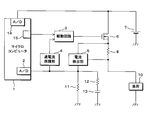
- FIG. 2 is a block diagram showing a schematic configuration of the embodiment of the power supply control device.
- the power supply control device includes a microcomputer 1, a drive circuit 3, an overcurrent protection unit 4, a current detection unit 5, a semiconductor switching element 6, a shunt resistor 8, resistors 11 and 12, and a capacitor 13.
- the semiconductor switching element 6 is an N-channel FET (Field Effect Transistor). With respect to the semiconductor switching element 6, the positive electrode of the battery 7 as a power source is connected to the drain, and the positive terminal of the load 10 is connected to the source through the shunt resistor 8. The negative terminal of the battery 7 and the negative terminal of the load 10 are grounded.
- the drive circuit 3 is connected to the gate of the semiconductor switching element 6, and the drive circuit 3 turns the semiconductor switching element 6 on or off based on the PWM signal given from the output terminal 15 of the microcomputer 1.
- the PWM signal is composed of a high level voltage and a low level voltage lower than the high level voltage. In the PWM signal, the high level voltage and the low level voltage are alternately repeated.
- the drive circuit 3 turns on the semiconductor switching element 6 when the PWM signal indicates a high level voltage, and turns off the semiconductor switching element 6 when the PWM signal indicates a low level voltage. Thus, switching of the semiconductor switching element 6 is performed by PWM control.
- the PWM control is performed according to the PWM signal.
- the drive circuit 3 increases the voltage of the gate of the semiconductor switching element 6 with reference to the ground potential. Thereby, in the semiconductor switching element 6, the gate voltage with reference to the source potential becomes a certain voltage or more, and the semiconductor switching element 6 is turned on. When the semiconductor switching element 6 is on, current flows from the positive terminal of the battery 7 in the order of the semiconductor switching element 6, the shunt resistor 8, and the load 10, and the battery 7 supplies power to the load 10 via the semiconductor switching element 6. Supply. In addition, the drive circuit 3 reduces the voltage of the gate of the semiconductor switching element 6 with reference to the ground potential. As a result, in the semiconductor switching element 6, the gate voltage relative to the source potential becomes less than a certain voltage, and the semiconductor switching element is turned off. When the semiconductor switching element 6 is off, no current flows between the drain and the source of the semiconductor switching element 6 and the power supply to the load 10 is stopped.
- Both terminals of the shunt resistor (current circuit) 8 are connected to the current detection unit (current circuit) 5 respectively.
- a shunt current whose current value is proportional to the current value of the current flowing through the shunt resistor 8 is output from the current detector 5.
- the current value of the shunt current is a predetermined fraction of the current value of the current flowing through the shunt resistor 8. Accordingly, the larger the current value of the current flowing through the semiconductor switching element 6 and the shunt resistor 8, the greater the current value of the shunt current.
- the shunt current output from the current detector 5 flows to the ground terminal through the resistor 11, and current / voltage conversion of the shunt current is performed.
- a low-pass filter in which a resistor 12 and a capacitor 13 are connected in series is connected to the resistor 11 in parallel.
- the resistor 11, the resistor 12, and the capacitor 13 constitute a filter circuit.
- the resistor 11 performs current / voltage conversion of the shunt current, and the converted voltage is filtered by the low-pass filter (12, 13).
- the voltage filtered by the low-pass filters (12, 13) is given to the overcurrent protection unit 4 and the microcomputer 1.
- the voltage value of the voltage filtered by the low-pass filter (12, 13) is larger as the current value of the shunt current is larger.
- the overcurrent protection unit (overcurrent protection circuit) 4 passes through the semiconductor switching element 6 through the drive circuit 3. Turn off to protect. At this time, the drive circuit 3 turns off the semiconductor switching element 6 regardless of the PWM signal output from the microcomputer 1. When the voltage value of the voltage filtered by the low-pass filter (12, 13) is equal to or lower than a predetermined voltage value, the drive circuit 3 turns on or off the semiconductor switching element 6 based on the PWM signal supplied from the output terminal 15 of the microcomputer 1. Turn off.
- the microcomputer 1 includes A / D (Analog / Digital) conversion units 14 and 2 that convert analog values into digital values, and an output terminal 15.
- the microcomputer 1 acquires the voltage value of the voltage filtered by the low-pass filter (12, 13) through the A / D converter 2 at a timing near the end of each pulse of the PWM signal output from the output terminal 15 (voltage detection). Part).
- the vicinity of the end of each pulse is preferably a period from the end of the corresponding period to the end of the time within 1% of the corresponding period. For example, when the period of the PWM signal is 100 ms, the vicinity of the pulse end is a period of 1 ms before the end of the pulse arrives. Note that a period before and after the end may be included in the vicinity of the end of each pulse.
- the microcomputer 1 estimates the wire temperature of the wire through which a current flows together with the semiconductor switching element 6 based on the voltage value acquired by the A / D conversion unit 2 (temperature estimation unit).
- a semiconductor switching element 6 and a shunt resistor 8 are provided in the middle of the electric wire.
- an estimation method for estimating the electric wire temperature for example, an estimation method performed by the electric wire protection device for a vehicle described in Patent Document 1 can be used.
- the microcomputer 1 When the estimated electric wire temperature exceeds a predetermined temperature, the microcomputer 1 turns off the semiconductor switching element 6 through the output terminal 15 and the drive circuit 3 (electric wire protection unit). At this time, the microcomputer 1 turns off the semiconductor switching element 6 by switching the voltage indicated by the PWM signal to the low level voltage. Thereafter, the microcomputer 1 maintains the voltage indicated by the PWM signal at a low level voltage.
- the microcomputer 1 acquires the voltage value (hereinafter referred to as a power supply voltage value) of the battery 7 as a power source through the A / D conversion unit 14.
- the microcomputer 1 calculates the duty ratio of the PWM signal based on the acquired power supply voltage value and a predetermined voltage value to be applied to the load 10.
- the microcomputer 1 calculates the duty ratio by, for example, a calculation formula, (predetermined voltage value / power supply voltage value) ⁇ 100%.
- the microcomputer 1 outputs a PWM signal based on the calculated duty ratio from the output terminal 15 and gives it to the drive circuit 3. At this time, the duty ratio of the PWM signal matches the duty ratio calculated by the microcomputer 1.
- the duty ratio indicates a ratio of a period during which the PWM signal indicates a high level voltage in one cycle.
- the microcomputer 1 outputs from the output terminal 15 a PWM signal in which the end of each cycle coincides with the end of each pulse. That is, in the PWM signal, the duty ratio is adjusted by adjusting the time point when the low level voltage is switched to the high level voltage, and the switching from the high level voltage to the low level voltage is periodically performed.
- the drive circuit 3 switches the semiconductor switching element 6 on or off based on the PWM signal given from the microcomputer 1 as described above. Therefore, with respect to switching of the semiconductor switching element 6, the duty ratio is adjusted by adjusting the switching point from OFF to ON, and switching from ON to OFF is performed periodically.
- the microcomputer 1 acquires the voltage value of the battery 7 through the A / D conversion unit 14. Next, the microcomputer 1 calculates the duty ratio of the PWM signal based on the acquired power supply voltage value and the predetermined voltage value, and outputs the PWM signal based on the calculated duty ratio from the output terminal 15. The drive circuit 3 turns on or off the semiconductor switching element 6 based on the PWM signal given from the microcomputer 1.
- the current detection unit 5 outputs a shunt current whose current value is proportional to the current value of the current passed through the semiconductor switching element 6 and applied to the load 10.
- the output shunt current is converted into a voltage by the resistor 11. .
- the voltage converted by the resistor 11 is filtered by the low-pass filter (12, 13).
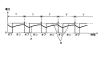
- FIG. 3 is a waveform diagram showing an example of a voltage waveform of a voltage obtained by converting the shunt current output from the current detection unit 5 by the resistor 11.
- A is an example of a voltage waveform of the voltage filtered by the low-pass filter (12, 13)
- B is a voltage when the low-pass filter (12, 13) does not exist and the filtering is not performed. It is an example of a waveform.
- the overcurrent protection unit 4 passes the semiconductor switching element 6 through the drive circuit 3. Turn off. At this time, the drive circuit 3 turns off the semiconductor switching element 6 regardless of the PWM signal.
- the low-pass filters (12, 13) filter the voltage converted by the resistor 11. For this reason, when an inrush current flows through the load 10, the peak voltage of the voltage converted by the resistor 11 is suppressed. As a result, it is possible to prevent the semiconductor switching element 6 from being turned off when an inrush current flows.
- the voltage value of the voltage filtered by the low-pass filter (12, 13) is expressed by the product of the current value of the shunt current output from the current detector 5 and the resistance value between both ends of the resistor 11. Is done.
- the resistance value between both ends of the resistor 11 increases as the electric power stored in the capacitor 13 increases.
- the resistance value between both ends of the resistor 11 is substantially the same as the resistance value of the parallel circuit in which the resistors 11 and 12 are connected in parallel, and is the smallest.
- the resistance value across the resistor 11 substantially matches the resistance value of the resistor 11. The biggest.
- the capacitor 13 When the semiconductor switching element 6 is on, the capacitor 13 is charged. When the semiconductor switching element 6 is off, a current flows from the capacitor 13 in the order of the resistors 12 and 11, and the capacitor 13 is discharged. At the time when the semiconductor switching element 6 is turned on to turn on the load 10, since the semiconductor switching element 6 is off for a long time, the power stored in the capacitor 13 is very small. For this reason, the resistance value between both ends of the resistor 11 is very small. As a result, the current value of the shunt current necessary for the voltage value of the voltage filtered by the low-pass filter (12, 13) to become a predetermined voltage value is large.
- the current value of the shunt current output from the current detector 5 is proportional to the current value of the current flowing through the shunt resistor 8. Therefore, in order to start the load 10, when the semiconductor switching element 6 is turned on from off, the upper limit value related to the current value of the current that can flow through the semiconductor switching element 6 is large.
- the waveform shape of the PWM signal output from the microcomputer 1 substantially matches the shape of the waveform B shown in FIG.
- the microcomputer 1 acquires the voltage value of the voltage filtered by the low-pass filter (12, 13) through the A / D conversion unit 2 at a timing near the end of each pulse of the PWM signal.
- the vicinity of the end of each pulse is, for example, the period from the time point that is within 1% of the period T from the end point to the end point.
- the timing in the vicinity of the end of each pulse coincides with the timing indicated by the arrow in FIG.
- the end of each period T and the end of each pulse coincide with each other as described above.
- the microcomputer 1 acquires the voltage value of the voltage filtered by the low-pass filter (12, 13) at the timing near the end of each pulse of the PWM signal. For this reason, the microcomputer 1 can acquire the substantially maximum value of the voltage value of the voltage filtered by the low-pass filter (12, 13). This maximum value indicates a current value larger than the actual current value (average current value) of the current flowing through the electric wire.
- the microcomputer 1 estimates the wire temperature of the wire through which a current flows together with the semiconductor switching element 6 based on the voltage value acquired by the A / D conversion unit 2.
- the microcomputer 1 turns off the semiconductor switching element 6 through the output terminal 15 when the estimated wire temperature exceeds a predetermined temperature.
- the microcomputer 1 turns off the semiconductor switching element 6 by switching the voltage indicated by the PWM signal to the low level voltage.
- the semiconductor switching element is used before the wire smokes. 6 can be reliably turned off.
- the microcomputer 1 may acquire a voltage value indicating a current value smaller than the average current value. For this reason, it is necessary to determine the minimum duty ratio that can be used for the time constant of the low-pass filter and the period T of the PWM signal that are set in advance.
- FIG. 4 is a characteristic diagram showing an example of overcurrent protection characteristics and electric wire smoke generation characteristics of the power supply control device.
- the vertical axis represents the current flow value of the electric wire
- the horizontal axis represents time or continuous current flow time.
- time is shown on the horizontal axis.
- covering material of an electric wire smokes by overheating indicates the electric wire temperature at which smoking starts in the curve indicating the electric wire temperature when the current flows through the passage time.
- the curve D indicating the cutoff threshold value via the microcomputer 1 based on the temperature calculation is set to a slightly low temperature side (low current side, short time side) of the wire smoke characteristic curve C.
- the larger the flow current value the shorter the flow time for the electric wire to reach smoke generation.
- this power supply control device requires time for calculating the wire temperature.
- blocking threshold value by temperature calculation is not set in the area
- the threshold value (predetermined voltage value) G of the overcurrent protection unit 4 is set as a current value slightly lower than the cutoff threshold value related to the temperature calculation of the microcomputer 1 when the conduction time is 10 milliseconds.
- the threshold G of the overcurrent protection unit 4 is constant, but the peak voltage of the inrush current is suppressed by the low-pass filter (CR filter) (12, 13) so as not to exceed the electric wire smoke generation characteristic C.
- the threshold G of the overcurrent protection unit 4 is substantially increased by the amount of voltage suppressed by the low-pass filter (12, 13). Note that an inrush current that does not suppress the peak voltage flows through the semiconductor switching element 6.
- the threshold G of the overcurrent protection unit 4 does not exceed the electric wire smoke generation characteristic C in the region where the cutoff threshold D is not set. Accordingly, even in this region, the current value can exceed the threshold value G before reaching the wire smoke characteristics C regardless of the current flow time. Therefore, in this power supply control device, the semiconductor switching element 6 and the electric wire can be protected without leakage from the load current F including the inrush current.
Landscapes
- Engineering & Computer Science (AREA)
- Power Engineering (AREA)
- Emergency Protection Circuit Devices (AREA)
- Protection Of Static Devices (AREA)
- Dc-Dc Converters (AREA)
- Control Of Electrical Variables (AREA)
Abstract
Description
また、マイコンは、半導体スイッチング素子を通流する電流の電流値を取得し、取得した電流値と、電流の通流時間とに基づき、半導体スイッチング素子と共に電流が通流する電線の温度を推定する。マイコンは、推定した温度に基づき、半導体スイッチング素子をオフにして、電線を保護する。
この場合、電線発煙特性Cに示すように、通流電流値が大きい程、電線が発煙に到る通流時間は短い。また、電線温度を演算するための時間が必要である。このため、温度演算による遮断閾値を示す曲線Dは、通流時間が例えば10ミリ秒以下である領域では設定されていない。
ところが、過電流自己保護回路の閾値Eを高い値に設定した場合、遮断閾値D(図1)が設定されていない領域で、閾値Eが電線発煙特性Cを超える領域が生じる。この領域では、通流電流値が、閾値Eを超えないが電線発煙特性Cを超える可能性がある。この場合、通流電流値が、過電流自己保護回路の閾値Eも温度演算による遮断閾値(不設定)も超えることなく、電線発煙特性Cを超えて電線が発煙し、電線を保護できないという問題がある。
電圧検出部は、PWM信号の各パルスの終端近傍のタイミングで、フィルタ回路が濾波した電圧の電圧値を検出する。温度推定部は、電圧検出部が検出した電圧値に基づき、半導体スイッチング素子と共に電流が通流する電線の温度を推定する。電線保護部は、温度推定部が推定した温度に基づき、半導体スイッチング素子をオフにする。
図2は、給電制御装置の実施の形態の概略構成を示すブロック図である。
この給電制御装置は、マイコン1、駆動回路3、過電流保護部4、電流検出部5、半導体スイッチング素子6、分流抵抗8、抵抗11,12及びコンデンサ13を備えている。
半導体スイッチング素子6は、Nチャネル型のFET(Field Effect Transistor)である。半導体スイッチング素子6について、ドレインに電源であるバッテリ7のプラス極が接続され、ソースに分流抵抗8を通じて負荷10のプラス端子が接続されている。バッテリ7のマイナス端子と、負荷10のマイナス端子とは接地されている。
また、駆動回路3は、接地電位を基準とした半導体スイッチング素子6のゲートの電圧を低下させる。これにより、半導体スイッチング素子6において、ソースの電位を基準としたゲートの電圧が一定電圧未満となり、半導体スイッチング素子はオフとなる。半導体スイッチング素子6がオフである場合、半導体スイッチング素子6のドレイン及びソース間に電流は流れず、負荷10への給電が停止する。
抵抗11が分流電流の電流/電圧変換を行い、変換した電圧はローパスフィルタ(12,13)によって濾波される。ローパスフィルタ(12,13)が濾波した電圧は、過電流保護部4及びマイコン1に与えられる。ローパスフィルタ(12,13)が濾波した電圧の電圧値は、分流電流の電流値が大きい程、大きい。
マイコン1は、電源であるバッテリ7の電圧値(以下、電源電圧値と記載する)を、A/D変換部14を通じて取得する。マイコン1は、取得した電源電圧値と、負荷10に印加すべき所定電圧値とに基づき、PWM信号のデューティ比を算出する。マイコン1は、デューティ比を、例えば、算出式、(所定電圧値/電源電圧値)×100%により算出する。
駆動回路3は、マイコン1から与えられたPWM信号に基づき、前述したように、半導体スイッチング素子6をオン又はオフに切替える。従って、半導体スイッチング素子6のスイッチングについては、オフからオンへの切替え時点を調整することによってデューティ比が調整され、オンからオフへの切替えは周期的に行われる。
マイコン1は、A/D変換部14を通じて、バッテリ7の電圧値を取得する。次に、マイコン1は、取得した電源電圧値と所定電圧値とに基づき、PWM信号のデューティ比を算出し、算出したデューティ比に基づくPWM信号を出力端子15から出力する。
駆動回路3は、マイコン1から与えられたPWM信号に基づき、半導体スイッチング素子6をオン又はオフにする。
図3は、電流検出部5が出力した分流電流が、抵抗11により変換された電圧の電圧波形の例を示す波形図である。ここで、Aは、ローパスフィルタ(12,13)により濾波された電圧の電圧波形の例であり、Bは、ローパスフィルタ(12,13)が存在せず、濾波が行われなかった場合の電圧波形の例である。
ここで、前述したように、電線を流れる電流の実電流値(平均電流値)よりも大きい電流値を示す電圧値に基づき、電線温度を推定するので、電線が発煙する前に、半導体スイッチング素子6を確実にオフにすることができる。
また、この給電制御装置では、電線温度を演算するための時間が必要である。このため、温度演算による遮断閾値を示す曲線Dは、通流時間が例えば10ミリ秒以下である領域では設定されていない。
また、過電流保護部4の閾値(所定電圧値)Gは、通流時間が10ミリ秒である場合におけるマイコン1の温度演算に係る遮断閾値より少し低い電流値として定めてられている。
以上により、遮断閾値Dが設定されていない領域で、過電流保護部4の閾値Gが電線発煙特性Cを超えることがない。従って、この領域でも、通流電流値は電線発煙特性Cに達する前に、通流時間に関係なく閾値Gを超えることができる。従って、この給電制御装置では、突入電流を含む負荷電流Fから漏れなく、半導体スイッチング素子6及び電線を保護することができる。
2 A/D変換部(電圧検出部)
3 駆動回路
4 過電流保護部(過電流保護回路)
5 電流検出部(電流回路)
6 半導体スイッチング素子
7 バッテリ
8 分流抵抗(電流回路)
10 負荷
11,12 抵抗(フィルタ回路)
13 コンデンサ(フィルタ回路)
14 A/D変換部
15 出力端子
Claims (3)
- PWM制御によりスイッチングが行われる半導体スイッチング素子と、
前記PWM制御に係るPWM信号を出力するPWM信号出力部と、
前記半導体スイッチング素子に通流する電流に関連する電流を出力する電流回路と、
該電流回路が出力した電流を電圧に変換し、変換した電圧を濾波するフィルタ回路と、
該フィルタ回路が濾波した電圧の電圧値に基づき、前記半導体スイッチング素子をオフにする過電流保護回路と、
前記PWM信号の各パルスの終端近傍のタイミングで、前記フィルタ回路が濾波した電圧の電圧値を検出する電圧検出部と、
該電圧検出部が検出した電圧値に基づき、前記半導体スイッチング素子と共に電流が通流する電線の温度を推定する温度推定部と、
該温度推定部が推定した温度に基づき、前記半導体スイッチング素子をオフにする電線保護部と
を備えることを特徴とする給電制御装置。 - 前記PWM信号出力部は、各周期の終端と各パルスの終端とが一致するPWM信号を出力するように構成してあること
を特徴とする請求項1に記載の給電制御装置。 - 前記各パルスの終端近傍は、該終端から、対応する周期の1%以内の時間を遡った時点から、該終端までの期間であること
を特徴とする請求項1又は2に記載の給電制御装置。
Priority Applications (4)
| Application Number | Priority Date | Filing Date | Title |
|---|---|---|---|
| EP17738533.3A EP3404790B1 (en) | 2016-01-15 | 2017-01-13 | Power supply control device |
| JP2017561184A JP6402833B2 (ja) | 2016-01-15 | 2017-01-13 | 給電制御装置 |
| CN201780005244.0A CN108475912B (zh) | 2016-01-15 | 2017-01-13 | 供电控制装置 |
| US16/063,820 US10998712B2 (en) | 2016-01-15 | 2017-01-13 | Power supply control apparatus having a wire protection unit |
Applications Claiming Priority (2)
| Application Number | Priority Date | Filing Date | Title |
|---|---|---|---|
| JP2016006371 | 2016-01-15 | ||
| JP2016-006371 | 2016-01-15 |
Publications (1)
| Publication Number | Publication Date |
|---|---|
| WO2017122781A1 true WO2017122781A1 (ja) | 2017-07-20 |
Family
ID=59311275
Family Applications (1)
| Application Number | Title | Priority Date | Filing Date |
|---|---|---|---|
| PCT/JP2017/001022 Ceased WO2017122781A1 (ja) | 2016-01-15 | 2017-01-13 | 給電制御装置 |
Country Status (5)
| Country | Link |
|---|---|
| US (1) | US10998712B2 (ja) |
| EP (1) | EP3404790B1 (ja) |
| JP (1) | JP6402833B2 (ja) |
| CN (1) | CN108475912B (ja) |
| WO (1) | WO2017122781A1 (ja) |
Cited By (3)
| Publication number | Priority date | Publication date | Assignee | Title |
|---|---|---|---|---|
| JP2022189584A (ja) * | 2021-06-11 | 2022-12-22 | 矢崎総業株式会社 | 電流検出装置及び電源装置 |
| JP2023144662A (ja) * | 2022-03-28 | 2023-10-11 | 古河電気工業株式会社 | 保護装置 |
| JP2023147410A (ja) * | 2022-03-30 | 2023-10-13 | 古河電気工業株式会社 | 保護装置 |
Families Citing this family (11)
| Publication number | Priority date | Publication date | Assignee | Title |
|---|---|---|---|---|
| JP6790350B2 (ja) * | 2015-12-03 | 2020-11-25 | 株式会社オートネットワーク技術研究所 | 給電制御装置 |
| JP6323485B2 (ja) * | 2016-03-24 | 2018-05-16 | 株式会社オートネットワーク技術研究所 | 給電制御装置 |
| JP6882023B2 (ja) * | 2017-03-13 | 2021-06-02 | 矢崎総業株式会社 | 電線保護装置 |
| JP6760215B2 (ja) * | 2017-06-22 | 2020-09-23 | 株式会社オートネットワーク技術研究所 | 電圧検出器及び信号出力装置 |
| JP6755399B2 (ja) * | 2017-07-03 | 2020-09-16 | 三菱電機株式会社 | 半導体スイッチング素子の短絡保護回路 |
| CN113491047A (zh) * | 2019-01-24 | 2021-10-08 | 西门子股份公司 | 电网上的负载区的运行 |
| JP7124730B2 (ja) * | 2019-01-29 | 2022-08-24 | 株式会社オートネットワーク技術研究所 | 給電制御装置及び給電制御方法 |
| JP7127736B2 (ja) | 2019-04-26 | 2022-08-30 | 株式会社オートネットワーク技術研究所 | 電流検出装置及び給電制御装置 |
| CN110543206A (zh) * | 2019-08-28 | 2019-12-06 | 歌尔股份有限公司 | 电流电压调节方法、装置、设备及存储介质 |
| JP7301243B2 (ja) * | 2020-12-24 | 2023-06-30 | 三菱電機株式会社 | ゲート駆動回路及び電力変換装置 |
| CN115776095A (zh) * | 2021-09-09 | 2023-03-10 | 施耐德电器工业公司 | 电机热过载保护方法 |
Citations (2)
| Publication number | Priority date | Publication date | Assignee | Title |
|---|---|---|---|---|
| JP2012054804A (ja) * | 2010-09-02 | 2012-03-15 | Yazaki Corp | 負荷駆動回路の保護装置 |
| JP2013229965A (ja) * | 2012-04-24 | 2013-11-07 | Yazaki Corp | 通電回路の保護装置 |
Family Cites Families (20)
| Publication number | Priority date | Publication date | Assignee | Title |
|---|---|---|---|---|
| US6011416A (en) * | 1997-02-19 | 2000-01-04 | Harness System Technologies Research Ltd. | Switch circuit having excess-current detection function |
| JP5323451B2 (ja) * | 2007-11-16 | 2013-10-23 | 古河電気工業株式会社 | 電源供給装置及び電源供給方法 |
| JP4624400B2 (ja) | 2007-11-19 | 2011-02-02 | 株式会社オートネットワーク技術研究所 | 車両用の電線保護方法および電線保護装置 |
| ITMI20082356A1 (it) * | 2008-12-30 | 2010-06-30 | St Microelectronics Srl | Controllo di un sistema a commutazione risonante con monitoraggio della corrente di lavoro in una finestra di osservazione |
| US8044644B2 (en) * | 2009-04-03 | 2011-10-25 | Texas Instruments Incorporated | Symmetric sample and hold over-current sensing method and apparatus |
| JP5660358B2 (ja) * | 2009-09-25 | 2015-01-28 | 株式会社オートネットワーク技術研究所 | 電力供給制御装置 |
| JP5482055B2 (ja) * | 2009-09-25 | 2014-04-23 | 株式会社オートネットワーク技術研究所 | 電力供給制御装置 |
| JP5097229B2 (ja) * | 2010-03-01 | 2012-12-12 | 矢崎総業株式会社 | 過熱保護装置 |
| JP2011258623A (ja) * | 2010-06-07 | 2011-12-22 | Toshiba Corp | パワー半導体システム |
| CN201717818U (zh) * | 2010-06-09 | 2011-01-19 | 深圳市特尔佳科技股份有限公司 | 一种电涡流缓速器驱动控制器 |
| JP5639868B2 (ja) * | 2010-12-06 | 2014-12-10 | 矢崎総業株式会社 | 負荷回路の保護装置 |
| CN202261152U (zh) * | 2011-09-30 | 2012-05-30 | 衡阳中微科技开发有限公司 | 采用脉冲宽度调制技术的永磁发电机调压器 |
| JP2013128343A (ja) * | 2011-12-16 | 2013-06-27 | Auto Network Gijutsu Kenkyusho:Kk | 過電流保護回路 |
| US8780590B2 (en) * | 2012-05-03 | 2014-07-15 | Hong Kong Applied Science & Technology Research Institute Company, Ltd. | Output current estimation for an isolated flyback converter with variable switching frequency control and duty cycle adjustment for both PWM and PFM modes |
| TWI493844B (zh) * | 2012-11-29 | 2015-07-21 | Power Forest Technology | 電源轉換器控制電路 |
| CN106797117B (zh) * | 2014-10-30 | 2019-06-18 | 矢崎总业株式会社 | 车用电源控制装置及其控制方法 |
| JP6472076B2 (ja) * | 2015-03-06 | 2019-02-20 | Fdk株式会社 | 負荷電流制御装置 |
| JP6790350B2 (ja) * | 2015-12-03 | 2020-11-25 | 株式会社オートネットワーク技術研究所 | 給電制御装置 |
| US10298251B2 (en) * | 2016-04-08 | 2019-05-21 | Infineon Technologies Ag | Electronic switching and protection circuit |
| DE102017106896B4 (de) * | 2017-03-30 | 2023-02-02 | Infineon Technologies Ag | Elektronischer Schalter für elektronische Sicherung |
-
2017
- 2017-01-13 WO PCT/JP2017/001022 patent/WO2017122781A1/ja not_active Ceased
- 2017-01-13 JP JP2017561184A patent/JP6402833B2/ja active Active
- 2017-01-13 EP EP17738533.3A patent/EP3404790B1/en active Active
- 2017-01-13 CN CN201780005244.0A patent/CN108475912B/zh active Active
- 2017-01-13 US US16/063,820 patent/US10998712B2/en active Active
Patent Citations (2)
| Publication number | Priority date | Publication date | Assignee | Title |
|---|---|---|---|---|
| JP2012054804A (ja) * | 2010-09-02 | 2012-03-15 | Yazaki Corp | 負荷駆動回路の保護装置 |
| JP2013229965A (ja) * | 2012-04-24 | 2013-11-07 | Yazaki Corp | 通電回路の保護装置 |
Cited By (7)
| Publication number | Priority date | Publication date | Assignee | Title |
|---|---|---|---|---|
| JP2022189584A (ja) * | 2021-06-11 | 2022-12-22 | 矢崎総業株式会社 | 電流検出装置及び電源装置 |
| JP7425020B2 (ja) | 2021-06-11 | 2024-01-30 | 矢崎総業株式会社 | 電流検出装置及び電源装置 |
| US12074428B2 (en) | 2021-06-11 | 2024-08-27 | Yazaki Corporation | Current detecting device and power supply device |
| JP2023144662A (ja) * | 2022-03-28 | 2023-10-11 | 古河電気工業株式会社 | 保護装置 |
| JP7788908B2 (ja) | 2022-03-28 | 2025-12-19 | 古河電気工業株式会社 | 保護装置 |
| JP2023147410A (ja) * | 2022-03-30 | 2023-10-13 | 古河電気工業株式会社 | 保護装置 |
| JP7822223B2 (ja) | 2022-03-30 | 2026-03-02 | 古河電気工業株式会社 | 保護装置 |
Also Published As
| Publication number | Publication date |
|---|---|
| CN108475912A (zh) | 2018-08-31 |
| JP6402833B2 (ja) | 2018-10-10 |
| JPWO2017122781A1 (ja) | 2018-05-31 |
| US10998712B2 (en) | 2021-05-04 |
| US20190260200A1 (en) | 2019-08-22 |
| EP3404790A1 (en) | 2018-11-21 |
| CN108475912B (zh) | 2019-10-29 |
| EP3404790B1 (en) | 2021-07-14 |
| EP3404790A4 (en) | 2019-01-23 |
Similar Documents
| Publication | Publication Date | Title |
|---|---|---|
| JP6402833B2 (ja) | 給電制御装置 | |
| US10720768B2 (en) | Electronic circuit breaker | |
| JP6514324B2 (ja) | 電子回路遮断器 | |
| US9705394B2 (en) | Overcurrent protection power supply apparatus | |
| US9941782B2 (en) | Power supply device and method for limiting an output current of a power supply device | |
| JP6790350B2 (ja) | 給電制御装置 | |
| JP4158754B2 (ja) | 過電流検知方法および検知回路 | |
| JP6698631B2 (ja) | 電力変換装置およびその制御方法 | |
| KR102418750B1 (ko) | 전기 어플라이언스,특히 전기 자동차의 배터리 충전을 위한 배터리 충전기의 전력 공급 스테이지 | |
| JP2007159159A (ja) | 半導体素子の保護装置 | |
| US10176950B2 (en) | Latching relay drive circuit | |
| JP2013128343A (ja) | 過電流保護回路 | |
| US10468969B2 (en) | Electronic circuit and method for operating an electronic circuit | |
| JP5715363B2 (ja) | 誘導性負荷駆動装置 | |
| KR102295580B1 (ko) | 차량용 dc모터의 과전류 감지 제어장치 및 제어방법 | |
| JP7396240B2 (ja) | 過電流保護回路 | |
| JP5097229B2 (ja) | 過熱保護装置 | |
| US8411396B2 (en) | Preventing metal oxide varistor (MOV) from releasing smoke, smell, and/or sound | |
| JP5034750B2 (ja) | 電源制御回路 | |
| JP2010278866A (ja) | 半導体素子の保護装置 | |
| JP6323389B2 (ja) | Dc/dcコンバータ | |
| JP3586402B2 (ja) | バッテリ充電器 | |
| KR20210097806A (ko) | 전류 제한 디바이스를 포함하는 스위치 시스템 | |
| US12447840B2 (en) | Charging voltage converter on a vehicle, having reverse current blocking device | |
| JP2500064B2 (ja) | 比例弁駆動装置 |
Legal Events
| Date | Code | Title | Description |
|---|---|---|---|
| 121 | Ep: the epo has been informed by wipo that ep was designated in this application |
Ref document number: 17738533 Country of ref document: EP Kind code of ref document: A1 |
|
| ENP | Entry into the national phase |
Ref document number: 2017561184 Country of ref document: JP Kind code of ref document: A |
|
| NENP | Non-entry into the national phase |
Ref country code: DE |
|
| WWE | Wipo information: entry into national phase |
Ref document number: 2017738533 Country of ref document: EP |
|
| ENP | Entry into the national phase |
Ref document number: 2017738533 Country of ref document: EP Effective date: 20180816 |