WO2017125992A1 - 光学素子並びにそれを用いた表示装置及び受光装置 - Google Patents
光学素子並びにそれを用いた表示装置及び受光装置 Download PDFInfo
- Publication number
- WO2017125992A1 WO2017125992A1 PCT/JP2016/051210 JP2016051210W WO2017125992A1 WO 2017125992 A1 WO2017125992 A1 WO 2017125992A1 JP 2016051210 W JP2016051210 W JP 2016051210W WO 2017125992 A1 WO2017125992 A1 WO 2017125992A1
- Authority
- WO
- WIPO (PCT)
- Prior art keywords
- light
- sub
- substrate
- beam splitter
- image display
- Prior art date
- Legal status (The legal status is an assumption and is not a legal conclusion. Google has not performed a legal analysis and makes no representation as to the accuracy of the status listed.)
- Ceased
Links
Images






Classifications
-
- G—PHYSICS
- G02—OPTICS
- G02B—OPTICAL ELEMENTS, SYSTEMS OR APPARATUS
- G02B27/00—Optical systems or apparatus not provided for by any of the groups G02B1/00 - G02B26/00, G02B30/00
- G02B27/0081—Optical systems or apparatus not provided for by any of the groups G02B1/00 - G02B26/00, G02B30/00 with means for altering, e.g. enlarging, the entrance or exit pupil
-
- G—PHYSICS
- G02—OPTICS
- G02B—OPTICAL ELEMENTS, SYSTEMS OR APPARATUS
- G02B17/00—Systems with reflecting surfaces, with or without refracting elements
- G02B17/08—Catadioptric systems
-
- G—PHYSICS
- G02—OPTICS
- G02B—OPTICAL ELEMENTS, SYSTEMS OR APPARATUS
- G02B27/00—Optical systems or apparatus not provided for by any of the groups G02B1/00 - G02B26/00, G02B30/00
- G02B27/01—Head-up displays
- G02B27/017—Head mounted
- G02B27/0172—Head mounted characterised by optical features
-
- G—PHYSICS
- G02—OPTICS
- G02B—OPTICAL ELEMENTS, SYSTEMS OR APPARATUS
- G02B27/00—Optical systems or apparatus not provided for by any of the groups G02B1/00 - G02B26/00, G02B30/00
- G02B27/02—Viewing or reading apparatus
-
- G—PHYSICS
- G02—OPTICS
- G02B—OPTICAL ELEMENTS, SYSTEMS OR APPARATUS
- G02B6/00—Light guides; Structural details of arrangements comprising light guides and other optical elements, e.g. couplings
-
- G—PHYSICS
- G02—OPTICS
- G02B—OPTICAL ELEMENTS, SYSTEMS OR APPARATUS
- G02B6/00—Light guides; Structural details of arrangements comprising light guides and other optical elements, e.g. couplings
- G02B6/0001—Light guides; Structural details of arrangements comprising light guides and other optical elements, e.g. couplings specially adapted for lighting devices or systems
- G02B6/0011—Light guides; Structural details of arrangements comprising light guides and other optical elements, e.g. couplings specially adapted for lighting devices or systems the light guides being planar or of plate-like form
- G02B6/0033—Means for improving the coupling-out of light from the light guide
- G02B6/005—Means for improving the coupling-out of light from the light guide provided by one optical element, or plurality thereof, placed on the light output side of the light guide
- G02B6/0055—Reflecting element, sheet or layer
-
- G—PHYSICS
- G02—OPTICS
- G02C—SPECTACLES; SUNGLASSES OR GOGGLES INSOFAR AS THEY HAVE THE SAME FEATURES AS SPECTACLES; CONTACT LENSES
- G02C7/00—Optical parts
-
- G—PHYSICS
- G02—OPTICS
- G02C—SPECTACLES; SUNGLASSES OR GOGGLES INSOFAR AS THEY HAVE THE SAME FEATURES AS SPECTACLES; CONTACT LENSES
- G02C7/00—Optical parts
- G02C7/02—Lenses; Lens systems ; Methods of designing lenses
- G02C7/08—Auxiliary lenses; Arrangements for varying focal length
- G02C7/086—Auxiliary lenses located directly on a main spectacle lens or in the immediate vicinity of main spectacles
-
- H—ELECTRICITY
- H04—ELECTRIC COMMUNICATION TECHNIQUE
- H04N—PICTORIAL COMMUNICATION, e.g. TELEVISION
- H04N5/00—Details of television systems
- H04N5/64—Constructional details of receivers, e.g. cabinets or dust covers
-
- G—PHYSICS
- G02—OPTICS
- G02B—OPTICAL ELEMENTS, SYSTEMS OR APPARATUS
- G02B27/00—Optical systems or apparatus not provided for by any of the groups G02B1/00 - G02B26/00, G02B30/00
- G02B27/01—Head-up displays
- G02B27/017—Head mounted
- G02B2027/0178—Eyeglass type
Definitions
- the optical element of the present invention since light is branched / expanded by the sub beam splitter surface, it is possible to prevent the occurrence of a region (missing) where there is no light beam propagating inside the main substrate.
- the sub beam splitter surface may be disposed so that light is not reflected twice or more by the reflecting surface. According to the display device of the present invention, since the substrate having a certain thickness or more is disposed in front of the reflecting surface, the light beam reflected twice or more on the reflecting surface is eliminated, and the generation of stray light can be prevented.
- the display device of the present invention may include the optical element as described above and an emission optical system that emits light. According to the display device of the present invention, a region where no light beam exists (missing) does not occur, and the emission mechanism can be reduced in size and weight.
- the display device of the present invention when the light travels in the setting direction, there is light that does not pass through the main beam splitter surface and passes through the sub-substrate, so that the amount of light emitted to the outside from the first main beam splitter surface close to the incident position The difference from the amount of light emitted to the outside from the N-th main beam splitter surface far from the incident position becomes small, and the brightness (light amount) can be made uniform.
- the light receiving device of the present invention may include the optical element as described above and a light receiving optical system for detecting light.
- a region that falls out of the light beam (light beam that cannot receive light) is generated.
- the total luminous flux reaching the main beam splitter surface can be received. Therefore, according to the light receiving device of the present invention, sensing can be performed in any region in the light beam.
- the predetermined region where the sub beam splitter surface 230 is disposed is a position where the image display light L is reflected by the reflecting surface 212, reflected by the front surface 210a, and not reflected by the reflecting surface 212 again.
- the image display light L that is reflected twice or more by the reflection surface 212 is eliminated, and stray light is prevented from being generated.
- FIG. 10 is a diagram showing a schematic configuration of the light receiving device of the present invention and an optical path in the XY plane.
- the light receiving device 401 includes a light receiving unit (light receiving optical system) 440 that receives light and a light guide unit (optical element) 100 that guides light from the outside to the light receiving unit 440 while reflecting the light from the inside.
- the front surface 10a and the rear surface 10b travel in the ⁇ X direction (setting direction) while reflecting light alternately a plurality of times.
- the traveling light reaches the sub-beam splitter surface 30 (front surface 10a), and the sub-beam splitter surface 30 (front surface 10a) reflects the set ratio of the luminous flux of the incident light and reflects the light. Transmits a set ratio of luminous flux. That is, when the light reaches the sub-beam splitter surface 30 (front surface 10a), the light flux of the set ratio travels inside the main substrate 10, and the light flux of the set ratio enters the sub-substrate 20 inside. proceed.
- the sub beam splitter surface 30 is arranged between the front surface 10a of the main substrate 10 and the rear surface 20b of the sub substrate 20, but the main substrate 10 and the sub substrate 20 are arranged. It is good also as a structure which is arrange
- FIG. FIG. 11 is a diagram showing a schematic configuration of a light guide unit (optical element) of the present invention.
- the image display light L from the emission unit 40 is configured to enter the main substrate 10 from the right surface 10c.
- the image display light L enters the sub substrate from the right surface of the sub substrate. It is good also as a structure. In this case, since it is possible to avoid concentrating complicated processing on one substrate, productivity is improved. Further, when the width of the transmissive liquid crystal display 41 is reduced, it is not necessary to increase the number of main beam splitter surfaces inside the main substrate in order to cope with the range of movement of the observer in the X direction. Good.
- FIG. 12 is a diagram showing a schematic configuration of the light guide unit (optical element) of the present invention.
Landscapes
- Physics & Mathematics (AREA)
- General Physics & Mathematics (AREA)
- Optics & Photonics (AREA)
- Health & Medical Sciences (AREA)
- Ophthalmology & Optometry (AREA)
- General Health & Medical Sciences (AREA)
- Engineering & Computer Science (AREA)
- Multimedia (AREA)
- Signal Processing (AREA)
- Optical Elements Other Than Lenses (AREA)
Abstract
Description
なお、眼鏡型ディスプレイ101は右眼用であり、遠視状態の右眼Eの中心に原点を有したXYZ座標系を定義する。Y方向は観察者の前方であり、Z方向は観察者の上方であり、X方向(設定方向)は観察者の左方である。
光学系42は、表示領域の画像表示光Lを透過させるものである。そして、光学系42は、透過型液晶表示器41の前方に距離をあけて配置されている。これにより、光学系42は、表示領域の画像表示光Lを透過させながら、観察対象の虚像を形成する。
さらに、第二ビームスプリッタ面11bを透過した画像表示光Lは、第三ビームスプリッタ面11cに到達する。そこで、第三ビームスプリッタ面11cは、入射した画像表示光Lの光束の所定割合を反射させるとともに、画像表示光Lの光束の所定割合を透過させる。つまり、画像表示光Lcの光束を観察者の眼Eに向かって導く。
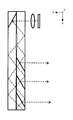
ここで、図6は、図4の眼鏡型ディスプレイ101のXY平面における光束の伝搬範囲を示す図であって、図中の符号Aは、光束の抜けを示している。
また、特開2011-164545号公報には、第一出射ユニットからの画像表示光を導くための第一ライトガイドと、第二出射ユニットからの画像表示光を導くための第二ライトガイドとを備える表示装置が開示されているが、2個の出射ユニットとを備えるので、大型化して重くなるという問題点がある。さらに、国際公開番号WO2011/24291には、前面と後面と上面と下面との4面で画像表示光を反射させて第二ライトガイドに導くための第一ライトガイドと、第一ライトガイドからの画像表示光を導くための第二ライトガイドとを備える表示装置が開示されているが、大型化して重くなるという問題点がある。
また、本発明の光学素子において、光が、前記主基板の前面及び後面並びに前記副基板の前面及び後面以外の面から入射するか、或いは、出射するようにしてもよい。
本発明の光学素子によれば、光が、主基板や副基板の内部に入射する位置や、主基板や副基板の内部から出射する位置の自由度を上げることができる。
本発明の表示装置によれば、反射面の前に一定以上の厚さの基板が配置されているため、反射面で2回以上反射する光束がなくなり、迷光の発生を防ぐことができる。
本発明の表示装置によれば、光束が存在しない領域(抜け)が発生せず、出射機構を小型化かつ軽量化することができる。
また、光が設定方向へ進行する際に、主ビームスプリッタ面を透過せず副基板内部を通過する光が存在するため、入射位置に近い第一主ビームスプリッタ面から外部に出射される光量と、入射位置から遠い位置の第N主ビームスプリッタ面から外部に出射される光量との差が小さくなり、明るさ(光量)を均一化することができる。
本発明の受光装置によれば、図4に示すような光学部品を受光装置に用いると、光束中に抜ける領域(受光不可となる光束)が発生してしまうが、本発明の受光装置によれば、主ビームスプリッタ面に到達した全光束を受光することができる。よって、本発明の受光装置によれば、センシング対象が光束中のどの領域に存在してもセンシングできる。
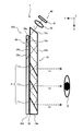
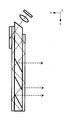
図1は本発明の眼鏡型ディスプレイ(表示装置)の概略構成及びXY平面における光路を示す図であり、図2は図1における光束の伝搬範囲を示す図である。なお、上述した眼鏡型ディスプレイ101と同様のものについては、同じ符号を付している。
眼鏡型ディスプレイ1は、眼鏡と似た外観をしており、画像表示光Lを出射する出射ユニット40と、出射ユニット40からの画像表示光Lを内部で反射させながら観察者の眼Eに導くライトガイドユニット(光学素子)100と、出射ユニット40とライトガイドユニット100とが取り付けられるフレーム部Fとを備える。
前面20aと後面20bとはX方向(設定方向)と平行になっている。つまり、前面10aと後面10bと前面20aと後面20bとはX方向(設定方向)と平行になっている。
そして、前面20aと後面20bとの間隔は、主基板10内部で伝搬する光束の抜けが発生しないように、設計者が計算式やシミュレーションソフト等を用いて主基板10内部に進行する画像表示光Lの光路と副基板20内部に進行する画像表示光Lの光路との差(ずれ)を考慮して決定した所定距離(厚さ)となっている。
上記副ビームスプリッタ面において光が反射及び透過する設定割合としては、主基板10内部で伝搬する光束の抜けを解消した範囲の明るさが、他の範囲の明るさとより均一になるように、設計者が計算式やシミュレーションソフト等を用いて設定した割合となっており、20%以上80%以下であることが好ましく、例えば50%等となる。
なお、副ビームスプリッタ面30は、主基板10と副基板20とを異なる屈折率の材料の組み合わせにより発生する反射を用いて形成してもよいし、主基板10と副基板20との間を接着剤や空気や油等の媒体で充填し、その媒体の屈折率と主基板10、副基板20の屈折率との差により生じる反射を利用して形成してもよい。
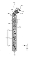
図8は本発明の眼鏡型ディスプレイ(表示装置)の概略構成及びXY平面における光路を示す図であり、図9は図8における光束の伝搬範囲を示す図である。なお、上述した眼鏡型ディスプレイ1と同様のものについては、同じ符号を付している。
眼鏡型ディスプレイ201は、眼鏡と似た外観をしており、画像表示光Lを出射する出射ユニット240と、出射ユニット240からの画像表示光Lを内部で反射させながら観察者の眼Eに導くライトガイドユニット(光学素子)200と、出射ユニット240とライトガイドユニット200とが取り付けられるフレーム部Fとを備える。
そして、副ビームスプリッタ面230は、例えば、主基板210の前面210aの所定領域上に光学コートにより形成されており、主基板210の前面210aと副基板20の後面20bとが直接接合されることで、主基板210の前面210aの所定領域と副基板20の後面20bの所定領域との間に配置されている。
なお、反射面212で1回反射した画像表示光Lは、前面20aまたは副ビームスプリッタ面230で反射した後に、再度、反射面212に入射しないよう、副基板20の厚さや、副ビームスプリッタ面230の領域を設定している。
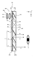
図10は本発明の受光装置の概略構成及びXY平面における光路を示す図である。なお、上述した眼鏡型ディスプレイ101と同様のものについては、同じ符号を付している。
受光装置401は、光を受光する受光ユニット(受光光学系)440と、外部からの光を内部で反射させながら受光ユニット440に導くライトガイドユニット(光学素子)100とを備える。
その後、主基板10内部を進行したり副基板20内部を進行したりした光が右面10cに到達する。そこで、右面10cから出射された光が受光ユニット440に導かれる。
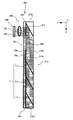
(1)上述した眼鏡型ディスプレイ1において、副ビームスプリッタ面30は、主基板10の前面10aと副基板20の後面20bとの間に配置される構成としたが、主基板10と副基板20の位置を入れ替えて、主基板10の後面10bと副基板20の前面20aとの間に配置されるような構成としてもよい。図11は、本発明のライトガイドユニット(光学素子)の概略構成を示す図である。
光が副ビームスプリッタ面によって分岐・拡大されるため、同光路長で光束が合成されて干渉縞が発生する場合があるが、このようなライトガイドユニットによれば、光路ずれや、光束の可干渉距離を超える光路長差を形成することができ、その結果、干渉縞が発生することを防止することができる。
10 主基板
11 主ビームスプリッタ面
20 副基板
30 副ビームスプリッタ面
40 出射ユニット
100 ライトガイドユニット(光学素子)
L 画像表示光
E 観察者の眼
Claims (6)
- 前面及び後面が設定方向と平行となり、光透過性材料で作製された主基板を備え、
前記主基板の内部には、前記設定方向に対して斜めに形成された少なくとも1個の主ビームスプリッタ面を有する光学素子であって、
前面及び後面が設定方向と平行となり、光透過性材料で作製された副基板を備え、
少なくとも1個の副基板の前面又は後面と、前記主基板の後面又は前面との間に、副ビームスプリッタ面が配置されていることを特徴とする光学素子。 - 光が、前記主基板の前面及び後面並びに前記副基板の前面及び後面以外の面から入射するか、或いは、出射することを特徴とする請求項1に記載の光学素子。
- 前記主基板又は前記副基板の内部には、反射面が形成されており、
光が、前記主基板の前面及び後面並びに前記副基板の前面及び後面の内の少なくとも1面から入射して前記反射面に到達するか、或いは、前記反射面に到達した後、前記主基板の前面及び後面並びに前記副基板の前面及び後面の内の少なくとも1面から出射することを特徴とする請求項1に記載の光学素子。 - 光が、前記反射面で2回以上反射しないように、前記副ビームスプリッタ面が配置されていることを特徴とする請求項3に記載の光学素子。
- 請求項2又は請求項3に記載の光学素子と、
光を出射する出射光学系とを備えることを特徴とする表示装置。 - 請求項2又は請求項3に記載の光学素子と、
光を検出する受光光学系とを備えることを特徴とする受光装置。
Priority Applications (5)
| Application Number | Priority Date | Filing Date | Title |
|---|---|---|---|
| JP2017562168A JP6562088B2 (ja) | 2016-01-18 | 2016-01-18 | 光学素子並びにそれを用いた表示装置及び受光装置 |
| US15/767,000 US11262564B2 (en) | 2016-01-18 | 2016-01-18 | Optical element, display device using same, and photoreceptor device |
| PCT/JP2016/051210 WO2017125992A1 (ja) | 2016-01-18 | 2016-01-18 | 光学素子並びにそれを用いた表示装置及び受光装置 |
| EP16886235.7A EP3407116B1 (en) | 2016-01-18 | 2016-01-18 | Optical element, display device using same, and photoreceptor device |
| TW106100380A TWI631368B (zh) | 2016-01-18 | 2017-01-06 | 光學元件以及使用該元件的顯示裝置和受光裝置 |
Applications Claiming Priority (1)
| Application Number | Priority Date | Filing Date | Title |
|---|---|---|---|
| PCT/JP2016/051210 WO2017125992A1 (ja) | 2016-01-18 | 2016-01-18 | 光学素子並びにそれを用いた表示装置及び受光装置 |
Publications (1)
| Publication Number | Publication Date |
|---|---|
| WO2017125992A1 true WO2017125992A1 (ja) | 2017-07-27 |
Family
ID=59361781
Family Applications (1)
| Application Number | Title | Priority Date | Filing Date |
|---|---|---|---|
| PCT/JP2016/051210 Ceased WO2017125992A1 (ja) | 2016-01-18 | 2016-01-18 | 光学素子並びにそれを用いた表示装置及び受光装置 |
Country Status (5)
| Country | Link |
|---|---|
| US (1) | US11262564B2 (ja) |
| EP (1) | EP3407116B1 (ja) |
| JP (1) | JP6562088B2 (ja) |
| TW (1) | TWI631368B (ja) |
| WO (1) | WO2017125992A1 (ja) |
Cited By (9)
| Publication number | Priority date | Publication date | Assignee | Title |
|---|---|---|---|---|
| WO2020049574A1 (en) | 2018-09-06 | 2020-03-12 | Lumus Ltd. | Near-eye display with laser diode illumination |
| JP2020536269A (ja) * | 2017-09-28 | 2020-12-10 | マジック リープ, インコーポレイテッドMagic Leap,Inc. | 光学結像システムの接眼レンズからの迷光放出を低減させる方法および装置 |
| EP3822694A4 (en) * | 2018-07-10 | 2021-06-23 | Shimadzu Corporation | IMAGE DISPLAY DEVICE |
| JP2021113929A (ja) * | 2020-01-20 | 2021-08-05 | 株式会社リコー | 導光部材および虚像表示装置 |
| JPWO2021157044A1 (ja) * | 2020-02-07 | 2021-08-12 | ||
| JP2021149008A (ja) * | 2020-03-19 | 2021-09-27 | 株式会社リコー | 導光体および虚像表示装置 |
| JP2022039935A (ja) * | 2020-08-28 | 2022-03-10 | 中強光電股▲ふん▼有限公司 | 光導波路、光導波路の製造方法及びヘッドマウント表示装置 |
| JP2022546979A (ja) * | 2019-09-16 | 2022-11-10 | ルーマス リミテッド | ビーム増倍を有する画像表示システム |
| US12449582B2 (en) | 2020-01-20 | 2025-10-21 | Ricoh Company, Ltd. | Light guide and virtual-image display device |
Families Citing this family (11)
| Publication number | Priority date | Publication date | Assignee | Title |
|---|---|---|---|---|
| IL237337B (en) * | 2015-02-19 | 2020-03-31 | Amitai Yaakov | A compact head-up display system with a uniform image |
| KR102655450B1 (ko) | 2017-02-22 | 2024-04-05 | 루머스 리미티드 | 광 가이드 광학 어셈블리 |
| US11415812B2 (en) | 2018-06-26 | 2022-08-16 | Lumus Ltd. | Compact collimating optical device and system |
| JP7398131B2 (ja) | 2019-03-12 | 2023-12-14 | ルムス エルティーディー. | 画像プロジェクタ |
| CN114080558B (zh) | 2019-07-04 | 2024-06-11 | 鲁姆斯有限公司 | 具有对称光束倍增的图像波导 |
| KR102893003B1 (ko) | 2019-09-16 | 2025-11-27 | 루머스 리미티드 | 헤드 마운트 디스플레이용 컴팩트 프로젝터 |
| EP4022380A4 (en) | 2019-12-05 | 2022-10-26 | Lumus Ltd. | LIGHT GUIDE OPTICAL ELEMENT USING COMPLEMENTARY COATED PARTIAL REFLECTORS, AND LIGHT GUIDE OPTICAL ELEMENT HAVING REDUCED LIGHT DIFFUSION |
| US12124037B2 (en) | 2020-05-24 | 2024-10-22 | Lumus Ltd. | Compound light-guide optical elements |
| US11886008B2 (en) | 2021-08-23 | 2024-01-30 | Lumus Ltd. | Methods of fabrication of compound light-guide optical elements having embedded coupling-in reflectors |
| JP2025526202A (ja) | 2022-08-18 | 2025-08-12 | ルムス エルティーディー. | 偏光カタディオプトリックコリメータを備えた画像プロジェクタ |
| WO2026104994A1 (en) * | 2024-11-12 | 2026-05-21 | 3M Innovative Properties Company | Optical system, optical waveguide, and light extracting mirror |
Citations (4)
| Publication number | Priority date | Publication date | Assignee | Title |
|---|---|---|---|---|
| JP2002162598A (ja) * | 2000-11-28 | 2002-06-07 | Olympus Optical Co Ltd | 観察光学系および撮像光学系 |
| JP2011186332A (ja) * | 2010-03-10 | 2011-09-22 | Shimadzu Corp | 表示装置 |
| JP2012058404A (ja) * | 2010-09-07 | 2012-03-22 | Shimadzu Corp | 光学部品及びそれを用いた表示装置 |
| JP2015096883A (ja) * | 2013-11-15 | 2015-05-21 | セイコーエプソン株式会社 | 光学素子および画像表示装置並びにこれらの製造方法 |
Family Cites Families (10)
| Publication number | Priority date | Publication date | Assignee | Title |
|---|---|---|---|---|
| EP1748305A4 (en) * | 2004-05-17 | 2009-01-14 | Nikon Corp | OPTICAL ELEMENT, COMBINER OPTICAL SYSTEM, AND IMAGE DISPLAY UNIT |
| IL173715A0 (en) * | 2006-02-14 | 2007-03-08 | Lumus Ltd | Substrate-guided imaging lens |
| US7589901B2 (en) * | 2007-07-10 | 2009-09-15 | Microvision, Inc. | Substrate-guided relays for use with scanned beam light sources |
| WO2011024291A1 (ja) | 2009-08-28 | 2011-03-03 | 株式会社島津製作所 | 表示装置 |
| JP5240214B2 (ja) | 2010-02-15 | 2013-07-17 | 株式会社島津製作所 | 表示装置 |
| JP5901192B2 (ja) * | 2011-09-13 | 2016-04-06 | オリンパス株式会社 | 光学機構 |
| US20130108229A1 (en) * | 2011-10-28 | 2013-05-02 | Google Inc. | Heads-up display including ambient light control |
| US9519092B1 (en) * | 2012-03-21 | 2016-12-13 | Google Inc. | Display method |
| IL237337B (en) * | 2015-02-19 | 2020-03-31 | Amitai Yaakov | A compact head-up display system with a uniform image |
| CN107924061B (zh) * | 2015-09-02 | 2020-11-17 | 索尼公司 | 光学装置及其制造方法和显示装置 |
-
2016
- 2016-01-18 WO PCT/JP2016/051210 patent/WO2017125992A1/ja not_active Ceased
- 2016-01-18 JP JP2017562168A patent/JP6562088B2/ja active Active
- 2016-01-18 US US15/767,000 patent/US11262564B2/en active Active
- 2016-01-18 EP EP16886235.7A patent/EP3407116B1/en active Active
-
2017
- 2017-01-06 TW TW106100380A patent/TWI631368B/zh not_active IP Right Cessation
Patent Citations (4)
| Publication number | Priority date | Publication date | Assignee | Title |
|---|---|---|---|---|
| JP2002162598A (ja) * | 2000-11-28 | 2002-06-07 | Olympus Optical Co Ltd | 観察光学系および撮像光学系 |
| JP2011186332A (ja) * | 2010-03-10 | 2011-09-22 | Shimadzu Corp | 表示装置 |
| JP2012058404A (ja) * | 2010-09-07 | 2012-03-22 | Shimadzu Corp | 光学部品及びそれを用いた表示装置 |
| JP2015096883A (ja) * | 2013-11-15 | 2015-05-21 | セイコーエプソン株式会社 | 光学素子および画像表示装置並びにこれらの製造方法 |
Non-Patent Citations (1)
| Title |
|---|
| See also references of EP3407116A4 * |
Cited By (22)
| Publication number | Priority date | Publication date | Assignee | Title |
|---|---|---|---|---|
| US12025802B2 (en) | 2017-09-28 | 2024-07-02 | Magic Leap, Inc. | Methods and apparatuses for reducing stray light emission from an eyepiece of an optical imaging system |
| JP2022093475A (ja) * | 2017-09-28 | 2022-06-23 | マジック リープ, インコーポレイテッド | 光学結像システムの接眼レンズからの迷光放出を低減させる方法および装置 |
| JP2020536269A (ja) * | 2017-09-28 | 2020-12-10 | マジック リープ, インコーポレイテッドMagic Leap,Inc. | 光学結像システムの接眼レンズからの迷光放出を低減させる方法および装置 |
| JP7296505B2 (ja) | 2017-09-28 | 2023-06-22 | マジック リープ, インコーポレイテッド | 光学結像システムの接眼レンズからの迷光放出を低減させる方法および装置 |
| JP7064581B2 (ja) | 2017-09-28 | 2022-05-10 | マジック リープ, インコーポレイテッド | 光学結像システムの接眼レンズからの迷光放出を低減させる方法および装置 |
| EP3822694A4 (en) * | 2018-07-10 | 2021-06-23 | Shimadzu Corporation | IMAGE DISPLAY DEVICE |
| EP3688517A4 (en) * | 2018-09-06 | 2021-03-03 | Lumus Ltd. | EYE DISPLAY WITH LASER DIODE ILLUMINATION |
| WO2020049574A1 (en) | 2018-09-06 | 2020-03-12 | Lumus Ltd. | Near-eye display with laser diode illumination |
| CN111149042A (zh) * | 2018-09-06 | 2020-05-12 | 鲁姆斯有限公司 | 具有激光二极管照明的近眼显示器 |
| JP2025067942A (ja) * | 2019-09-16 | 2025-04-24 | ルーマス リミテッド | ビーム増倍を有する画像表示システム |
| JP7638538B2 (ja) | 2019-09-16 | 2025-03-04 | ルーマス リミテッド | ビーム増倍を有する画像表示システム |
| JP7873514B2 (ja) | 2019-09-16 | 2026-06-12 | ルーマス リミテッド | ビーム増倍を有する画像表示システム |
| JP2022546979A (ja) * | 2019-09-16 | 2022-11-10 | ルーマス リミテッド | ビーム増倍を有する画像表示システム |
| JP2021113929A (ja) * | 2020-01-20 | 2021-08-05 | 株式会社リコー | 導光部材および虚像表示装置 |
| JP7380240B2 (ja) | 2020-01-20 | 2023-11-15 | 株式会社リコー | 導光部材および虚像表示装置 |
| US12449582B2 (en) | 2020-01-20 | 2025-10-21 | Ricoh Company, Ltd. | Light guide and virtual-image display device |
| JP7424396B2 (ja) | 2020-02-07 | 2024-01-30 | 株式会社島津製作所 | 表示装置及び該表示装置で用いる光学素子 |
| WO2021157044A1 (ja) * | 2020-02-07 | 2021-08-12 | 株式会社島津製作所 | 表示装置及び該表示装置で用いる光学素子 |
| JPWO2021157044A1 (ja) * | 2020-02-07 | 2021-08-12 | ||
| JP2021149008A (ja) * | 2020-03-19 | 2021-09-27 | 株式会社リコー | 導光体および虚像表示装置 |
| JP2022039935A (ja) * | 2020-08-28 | 2022-03-10 | 中強光電股▲ふん▼有限公司 | 光導波路、光導波路の製造方法及びヘッドマウント表示装置 |
| JP7666092B2 (ja) | 2020-08-28 | 2025-04-22 | 中強光電股▲ふん▼有限公司 | 光導波路、光導波路の製造方法及びヘッドマウント表示装置 |
Also Published As
| Publication number | Publication date |
|---|---|
| EP3407116A1 (en) | 2018-11-28 |
| TWI631368B (zh) | 2018-08-01 |
| EP3407116B1 (en) | 2025-06-25 |
| TW201743103A (zh) | 2017-12-16 |
| JPWO2017125992A1 (ja) | 2018-05-31 |
| US11262564B2 (en) | 2022-03-01 |
| US20180307014A1 (en) | 2018-10-25 |
| EP3407116A4 (en) | 2019-09-25 |
| JP6562088B2 (ja) | 2019-08-21 |
Similar Documents
| Publication | Publication Date | Title |
|---|---|---|
| JP6562088B2 (ja) | 光学素子並びにそれを用いた表示装置及び受光装置 | |
| US11054566B2 (en) | Display waveguide with a high-index layer | |
| US11143866B2 (en) | Waveguide including volume Bragg gratings | |
| JP6522158B2 (ja) | 積層された光導波路を有するニアアイディスプレイ | |
| JP5471986B2 (ja) | 光学部品及びそれを用いた表示装置 | |
| US10146054B2 (en) | Adding prescriptive correction to eyepieces for see-through head wearable displays | |
| US9465215B2 (en) | Lightguide with multiple in-coupling holograms for head wearable display | |
| US9274338B2 (en) | Increasing field of view of reflective waveguide | |
| CN104536088B (zh) | 齿形镶嵌平面波导光学器件 | |
| US20200117005A1 (en) | Waveguide for conveying multiple portions of field of view | |
| US10761332B2 (en) | Light-guiding device and display device | |
| EP4094116B1 (en) | Light guide and virtual-image display device | |
| JP2014224891A (ja) | 光学素子および表示装置 | |
| US11774753B1 (en) | Cascaded pupil-replicating waveguides | |
| US10890770B2 (en) | Waveguide having partial reflector | |
| JP2011186332A (ja) | 表示装置 | |
| JP2014222260A (ja) | 光学素子、表示装置、および光学素子の製造方法 | |
| JP5861332B2 (ja) | 表示装置 | |
| WO2023097806A1 (zh) | 光学模组和电子设备 | |
| JP7380240B2 (ja) | 導光部材および虚像表示装置 |
Legal Events
| Date | Code | Title | Description |
|---|---|---|---|
| 121 | Ep: the epo has been informed by wipo that ep was designated in this application |
Ref document number: 16886235 Country of ref document: EP Kind code of ref document: A1 |
|
| ENP | Entry into the national phase |
Ref document number: 2017562168 Country of ref document: JP Kind code of ref document: A |
|
| WWE | Wipo information: entry into national phase |
Ref document number: 15767000 Country of ref document: US |
|
| NENP | Non-entry into the national phase |
Ref country code: DE |
|
| WWE | Wipo information: entry into national phase |
Ref document number: 2016886235 Country of ref document: EP |
|
| ENP | Entry into the national phase |
Ref document number: 2016886235 Country of ref document: EP Effective date: 20180820 |
|
| WWG | Wipo information: grant in national office |
Ref document number: 2016886235 Country of ref document: EP |