WO2017126653A1 - Corps lié ainsi que procédé de fabrication de celui-ci, substrat pour module de puissance ainsi que procédé de fabrication de celui-ci, et module de puissance - Google Patents
Corps lié ainsi que procédé de fabrication de celui-ci, substrat pour module de puissance ainsi que procédé de fabrication de celui-ci, et module de puissance Download PDFInfo
- Publication number
- WO2017126653A1 WO2017126653A1 PCT/JP2017/001922 JP2017001922W WO2017126653A1 WO 2017126653 A1 WO2017126653 A1 WO 2017126653A1 JP 2017001922 W JP2017001922 W JP 2017001922W WO 2017126653 A1 WO2017126653 A1 WO 2017126653A1
- Authority
- WO
- WIPO (PCT)
- Prior art keywords
- ceramic substrate
- power module
- substrate
- ceramic
- circuit layer
- Prior art date
- Legal status (The legal status is an assumption and is not a legal conclusion. Google has not performed a legal analysis and makes no representation as to the accuracy of the status listed.)
- Ceased
Links
Images


Classifications
-
- H—ELECTRICITY
- H10—SEMICONDUCTOR DEVICES; ELECTRIC SOLID-STATE DEVICES NOT OTHERWISE PROVIDED FOR
- H10W—GENERIC PACKAGES, INTERCONNECTIONS, CONNECTORS OR OTHER CONSTRUCTIONAL DETAILS OF DEVICES COVERED BY CLASS H10
- H10W20/00—Interconnections in chips, wafers or substrates
- H10W20/40—Interconnections external to wafers or substrates, e.g. back-end-of-line [BEOL] metallisations or vias connecting to gate electrodes
- H10W20/41—Interconnections external to wafers or substrates, e.g. back-end-of-line [BEOL] metallisations or vias connecting to gate electrodes characterised by their conductive parts
- H10W20/44—Conductive materials thereof
- H10W20/4403—Conductive materials thereof based on metals, e.g. alloys, metal silicides
- H10W20/4421—Conductive materials thereof based on metals, e.g. alloys, metal silicides the principal metal being copper
-
- H—ELECTRICITY
- H10—SEMICONDUCTOR DEVICES; ELECTRIC SOLID-STATE DEVICES NOT OTHERWISE PROVIDED FOR
- H10W—GENERIC PACKAGES, INTERCONNECTIONS, CONNECTORS OR OTHER CONSTRUCTIONAL DETAILS OF DEVICES COVERED BY CLASS H10
- H10W40/00—Arrangements for thermal protection or thermal control
- H10W40/20—Arrangements for cooling
- H10W40/25—Arrangements for cooling characterised by their materials
- H10W40/255—Arrangements for cooling characterised by their materials having a laminate or multilayered structure, e.g. direct bond copper [DBC] ceramic substrates
-
- B—PERFORMING OPERATIONS; TRANSPORTING
- B23—MACHINE TOOLS; METAL-WORKING NOT OTHERWISE PROVIDED FOR
- B23K—SOLDERING OR UNSOLDERING; WELDING; CLADDING OR PLATING BY SOLDERING OR WELDING; CUTTING BY APPLYING HEAT LOCALLY, e.g. FLAME CUTTING; WORKING BY LASER BEAM
- B23K1/00—Soldering, e.g. brazing, or unsoldering
- B23K1/008—Soldering within a furnace
-
- B—PERFORMING OPERATIONS; TRANSPORTING
- B23—MACHINE TOOLS; METAL-WORKING NOT OTHERWISE PROVIDED FOR
- B23K—SOLDERING OR UNSOLDERING; WELDING; CLADDING OR PLATING BY SOLDERING OR WELDING; CUTTING BY APPLYING HEAT LOCALLY, e.g. FLAME CUTTING; WORKING BY LASER BEAM
- B23K35/00—Rods, electrodes, materials, or media, for use in soldering, welding, or cutting
- B23K35/02—Rods, electrodes, materials, or media, for use in soldering, welding, or cutting characterised by mechanical features, e.g. shape
- B23K35/0222—Rods, electrodes, materials, or media, for use in soldering, welding, or cutting characterised by mechanical features, e.g. shape for use in soldering or brazing
- B23K35/0233—Sheets or foils
- B23K35/0238—Sheets or foils layered
-
- B—PERFORMING OPERATIONS; TRANSPORTING
- B23—MACHINE TOOLS; METAL-WORKING NOT OTHERWISE PROVIDED FOR
- B23K—SOLDERING OR UNSOLDERING; WELDING; CLADDING OR PLATING BY SOLDERING OR WELDING; CUTTING BY APPLYING HEAT LOCALLY, e.g. FLAME CUTTING; WORKING BY LASER BEAM
- B23K35/00—Rods, electrodes, materials, or media, for use in soldering, welding, or cutting
- B23K35/22—Rods, electrodes, materials, or media, for use in soldering, welding, or cutting characterised by the composition or nature of the material
- B23K35/24—Selection of soldering or welding materials proper
- B23K35/26—Selection of soldering or welding materials proper with the principal constituent melting at less than 400°C
- B23K35/262—Sn as the principal constituent
-
- B—PERFORMING OPERATIONS; TRANSPORTING
- B23—MACHINE TOOLS; METAL-WORKING NOT OTHERWISE PROVIDED FOR
- B23K—SOLDERING OR UNSOLDERING; WELDING; CLADDING OR PLATING BY SOLDERING OR WELDING; CUTTING BY APPLYING HEAT LOCALLY, e.g. FLAME CUTTING; WORKING BY LASER BEAM
- B23K35/00—Rods, electrodes, materials, or media, for use in soldering, welding, or cutting
- B23K35/22—Rods, electrodes, materials, or media, for use in soldering, welding, or cutting characterised by the composition or nature of the material
- B23K35/24—Selection of soldering or welding materials proper
- B23K35/30—Selection of soldering or welding materials proper with the principal constituent melting at less than 1550°C
- B23K35/302—Cu as the principal constituent
-
- C—CHEMISTRY; METALLURGY
- C04—CEMENTS; CONCRETE; ARTIFICIAL STONE; CERAMICS; REFRACTORIES
- C04B—LIME, MAGNESIA; SLAG; CEMENTS; COMPOSITIONS THEREOF, e.g. MORTARS, CONCRETE OR LIKE BUILDING MATERIALS; ARTIFICIAL STONE; CERAMICS; REFRACTORIES; TREATMENT OF NATURAL STONE
- C04B35/00—Shaped ceramic products characterised by their composition; Ceramics compositions; Processing powders of inorganic compounds preparatory to the manufacturing of ceramic products
- C04B35/515—Shaped ceramic products characterised by their composition; Ceramics compositions; Processing powders of inorganic compounds preparatory to the manufacturing of ceramic products based on non-oxide ceramics
- C04B35/58—Shaped ceramic products characterised by their composition; Ceramics compositions; Processing powders of inorganic compounds preparatory to the manufacturing of ceramic products based on non-oxide ceramics based on borides, nitrides, i.e. nitrides, oxynitrides, carbonitrides or oxycarbonitrides or silicides
- C04B35/581—Shaped ceramic products characterised by their composition; Ceramics compositions; Processing powders of inorganic compounds preparatory to the manufacturing of ceramic products based on non-oxide ceramics based on borides, nitrides, i.e. nitrides, oxynitrides, carbonitrides or oxycarbonitrides or silicides based on aluminium nitride
-
- C—CHEMISTRY; METALLURGY
- C04—CEMENTS; CONCRETE; ARTIFICIAL STONE; CERAMICS; REFRACTORIES
- C04B—LIME, MAGNESIA; SLAG; CEMENTS; COMPOSITIONS THEREOF, e.g. MORTARS, CONCRETE OR LIKE BUILDING MATERIALS; ARTIFICIAL STONE; CERAMICS; REFRACTORIES; TREATMENT OF NATURAL STONE
- C04B35/00—Shaped ceramic products characterised by their composition; Ceramics compositions; Processing powders of inorganic compounds preparatory to the manufacturing of ceramic products
- C04B35/622—Forming processes; Processing powders of inorganic compounds preparatory to the manufacturing of ceramic products
- C04B35/64—Burning or sintering processes
- C04B35/645—Pressure sintering
-
- C—CHEMISTRY; METALLURGY
- C04—CEMENTS; CONCRETE; ARTIFICIAL STONE; CERAMICS; REFRACTORIES
- C04B—LIME, MAGNESIA; SLAG; CEMENTS; COMPOSITIONS THEREOF, e.g. MORTARS, CONCRETE OR LIKE BUILDING MATERIALS; ARTIFICIAL STONE; CERAMICS; REFRACTORIES; TREATMENT OF NATURAL STONE
- C04B37/00—Joining burned ceramic articles with other burned ceramic articles or other articles by heating
- C04B37/02—Joining burned ceramic articles with other burned ceramic articles or other articles by heating with metallic articles
- C04B37/023—Joining burned ceramic articles with other burned ceramic articles or other articles by heating with metallic articles characterised by the interlayer used
- C04B37/026—Joining burned ceramic articles with other burned ceramic articles or other articles by heating with metallic articles characterised by the interlayer used consisting of metals or metal salts
-
- C—CHEMISTRY; METALLURGY
- C22—METALLURGY; FERROUS OR NON-FERROUS ALLOYS; TREATMENT OF ALLOYS OR NON-FERROUS METALS
- C22C—ALLOYS
- C22C9/00—Alloys based on copper
- C22C9/02—Alloys based on copper with tin as the next major constituent
-
- H—ELECTRICITY
- H10—SEMICONDUCTOR DEVICES; ELECTRIC SOLID-STATE DEVICES NOT OTHERWISE PROVIDED FOR
- H10W—GENERIC PACKAGES, INTERCONNECTIONS, CONNECTORS OR OTHER CONSTRUCTIONAL DETAILS OF DEVICES COVERED BY CLASS H10
- H10W40/00—Arrangements for thermal protection or thermal control
- H10W40/01—Manufacture or treatment
- H10W40/03—Manufacture or treatment of arrangements for cooling
- H10W40/037—Assembling together parts thereof
-
- H—ELECTRICITY
- H10—SEMICONDUCTOR DEVICES; ELECTRIC SOLID-STATE DEVICES NOT OTHERWISE PROVIDED FOR
- H10W—GENERIC PACKAGES, INTERCONNECTIONS, CONNECTORS OR OTHER CONSTRUCTIONAL DETAILS OF DEVICES COVERED BY CLASS H10
- H10W40/00—Arrangements for thermal protection or thermal control
- H10W40/20—Arrangements for cooling
- H10W40/25—Arrangements for cooling characterised by their materials
- H10W40/258—Metallic materials
-
- H—ELECTRICITY
- H10—SEMICONDUCTOR DEVICES; ELECTRIC SOLID-STATE DEVICES NOT OTHERWISE PROVIDED FOR
- H10W—GENERIC PACKAGES, INTERCONNECTIONS, CONNECTORS OR OTHER CONSTRUCTIONAL DETAILS OF DEVICES COVERED BY CLASS H10
- H10W40/00—Arrangements for thermal protection or thermal control
- H10W40/20—Arrangements for cooling
- H10W40/25—Arrangements for cooling characterised by their materials
- H10W40/259—Ceramics or glasses
-
- H—ELECTRICITY
- H10—SEMICONDUCTOR DEVICES; ELECTRIC SOLID-STATE DEVICES NOT OTHERWISE PROVIDED FOR
- H10W—GENERIC PACKAGES, INTERCONNECTIONS, CONNECTORS OR OTHER CONSTRUCTIONAL DETAILS OF DEVICES COVERED BY CLASS H10
- H10W70/00—Package substrates; Interposers; Redistribution layers [RDL]
- H10W70/01—Manufacture or treatment
- H10W70/02—Manufacture or treatment of conductive package substrates serving as an interconnection, e.g. of metal plates
-
- H—ELECTRICITY
- H10—SEMICONDUCTOR DEVICES; ELECTRIC SOLID-STATE DEVICES NOT OTHERWISE PROVIDED FOR
- H10W—GENERIC PACKAGES, INTERCONNECTIONS, CONNECTORS OR OTHER CONSTRUCTIONAL DETAILS OF DEVICES COVERED BY CLASS H10
- H10W70/00—Package substrates; Interposers; Redistribution layers [RDL]
- H10W70/60—Insulating or insulated package substrates; Interposers; Redistribution layers
- H10W70/67—Insulating or insulated package substrates; Interposers; Redistribution layers characterised by their insulating layers or insulating parts
- H10W70/68—Shapes or dispositions thereof
- H10W70/6875—Shapes or dispositions thereof being on a metallic substrate, e.g. insulated metal substrates [IMS]
-
- B—PERFORMING OPERATIONS; TRANSPORTING
- B23—MACHINE TOOLS; METAL-WORKING NOT OTHERWISE PROVIDED FOR
- B23K—SOLDERING OR UNSOLDERING; WELDING; CLADDING OR PLATING BY SOLDERING OR WELDING; CUTTING BY APPLYING HEAT LOCALLY, e.g. FLAME CUTTING; WORKING BY LASER BEAM
- B23K2101/00—Articles made by soldering, welding or cutting
- B23K2101/36—Electric or electronic devices
- B23K2101/40—Semiconductor devices
-
- B—PERFORMING OPERATIONS; TRANSPORTING
- B23—MACHINE TOOLS; METAL-WORKING NOT OTHERWISE PROVIDED FOR
- B23K—SOLDERING OR UNSOLDERING; WELDING; CLADDING OR PLATING BY SOLDERING OR WELDING; CUTTING BY APPLYING HEAT LOCALLY, e.g. FLAME CUTTING; WORKING BY LASER BEAM
- B23K2103/00—Materials to be soldered, welded or cut
- B23K2103/16—Composite materials
- B23K2103/166—Multilayered materials
- B23K2103/172—Multilayered materials wherein at least one of the layers is non-metallic
-
- B—PERFORMING OPERATIONS; TRANSPORTING
- B23—MACHINE TOOLS; METAL-WORKING NOT OTHERWISE PROVIDED FOR
- B23K—SOLDERING OR UNSOLDERING; WELDING; CLADDING OR PLATING BY SOLDERING OR WELDING; CUTTING BY APPLYING HEAT LOCALLY, e.g. FLAME CUTTING; WORKING BY LASER BEAM
- B23K35/00—Rods, electrodes, materials, or media, for use in soldering, welding, or cutting
- B23K35/22—Rods, electrodes, materials, or media, for use in soldering, welding, or cutting characterised by the composition or nature of the material
- B23K35/24—Selection of soldering or welding materials proper
- B23K35/30—Selection of soldering or welding materials proper with the principal constituent melting at less than 1550°C
- B23K35/3006—Ag as the principal constituent
-
- C—CHEMISTRY; METALLURGY
- C04—CEMENTS; CONCRETE; ARTIFICIAL STONE; CERAMICS; REFRACTORIES
- C04B—LIME, MAGNESIA; SLAG; CEMENTS; COMPOSITIONS THEREOF, e.g. MORTARS, CONCRETE OR LIKE BUILDING MATERIALS; ARTIFICIAL STONE; CERAMICS; REFRACTORIES; TREATMENT OF NATURAL STONE
- C04B2235/00—Aspects relating to ceramic starting mixtures or sintered ceramic products
- C04B2235/02—Composition of constituents of the starting material or of secondary phases of the final product
- C04B2235/30—Constituents and secondary phases not being of a fibrous nature
- C04B2235/32—Metal oxides, mixed metal oxides, or oxide-forming salts thereof, e.g. carbonates, nitrates, (oxy)hydroxides, chlorides
- C04B2235/3231—Refractory metal oxides, their mixed metal oxides, or oxide-forming salts thereof
- C04B2235/3244—Zirconium oxides, zirconates, hafnium oxides, hafnates, or oxide-forming salts thereof
-
- C—CHEMISTRY; METALLURGY
- C04—CEMENTS; CONCRETE; ARTIFICIAL STONE; CERAMICS; REFRACTORIES
- C04B—LIME, MAGNESIA; SLAG; CEMENTS; COMPOSITIONS THEREOF, e.g. MORTARS, CONCRETE OR LIKE BUILDING MATERIALS; ARTIFICIAL STONE; CERAMICS; REFRACTORIES; TREATMENT OF NATURAL STONE
- C04B2235/00—Aspects relating to ceramic starting mixtures or sintered ceramic products
- C04B2235/65—Aspects relating to heat treatments of ceramic bodies such as green ceramics or pre-sintered ceramics, e.g. burning, sintering or melting processes
- C04B2235/656—Aspects relating to heat treatments of ceramic bodies such as green ceramics or pre-sintered ceramics, e.g. burning, sintering or melting processes characterised by specific heating conditions during heat treatment
- C04B2235/6562—Heating rate
-
- C—CHEMISTRY; METALLURGY
- C04—CEMENTS; CONCRETE; ARTIFICIAL STONE; CERAMICS; REFRACTORIES
- C04B—LIME, MAGNESIA; SLAG; CEMENTS; COMPOSITIONS THEREOF, e.g. MORTARS, CONCRETE OR LIKE BUILDING MATERIALS; ARTIFICIAL STONE; CERAMICS; REFRACTORIES; TREATMENT OF NATURAL STONE
- C04B2235/00—Aspects relating to ceramic starting mixtures or sintered ceramic products
- C04B2235/65—Aspects relating to heat treatments of ceramic bodies such as green ceramics or pre-sintered ceramics, e.g. burning, sintering or melting processes
- C04B2235/656—Aspects relating to heat treatments of ceramic bodies such as green ceramics or pre-sintered ceramics, e.g. burning, sintering or melting processes characterised by specific heating conditions during heat treatment
- C04B2235/6567—Treatment time
-
- C—CHEMISTRY; METALLURGY
- C04—CEMENTS; CONCRETE; ARTIFICIAL STONE; CERAMICS; REFRACTORIES
- C04B—LIME, MAGNESIA; SLAG; CEMENTS; COMPOSITIONS THEREOF, e.g. MORTARS, CONCRETE OR LIKE BUILDING MATERIALS; ARTIFICIAL STONE; CERAMICS; REFRACTORIES; TREATMENT OF NATURAL STONE
- C04B2237/00—Aspects relating to ceramic laminates or to joining of ceramic articles with other articles by heating
- C04B2237/02—Aspects relating to interlayers, e.g. used to join ceramic articles with other articles by heating
- C04B2237/12—Metallic interlayers
- C04B2237/121—Metallic interlayers based on aluminium
-
- C—CHEMISTRY; METALLURGY
- C04—CEMENTS; CONCRETE; ARTIFICIAL STONE; CERAMICS; REFRACTORIES
- C04B—LIME, MAGNESIA; SLAG; CEMENTS; COMPOSITIONS THEREOF, e.g. MORTARS, CONCRETE OR LIKE BUILDING MATERIALS; ARTIFICIAL STONE; CERAMICS; REFRACTORIES; TREATMENT OF NATURAL STONE
- C04B2237/00—Aspects relating to ceramic laminates or to joining of ceramic articles with other articles by heating
- C04B2237/02—Aspects relating to interlayers, e.g. used to join ceramic articles with other articles by heating
- C04B2237/12—Metallic interlayers
- C04B2237/122—Metallic interlayers based on refractory metals
-
- C—CHEMISTRY; METALLURGY
- C04—CEMENTS; CONCRETE; ARTIFICIAL STONE; CERAMICS; REFRACTORIES
- C04B—LIME, MAGNESIA; SLAG; CEMENTS; COMPOSITIONS THEREOF, e.g. MORTARS, CONCRETE OR LIKE BUILDING MATERIALS; ARTIFICIAL STONE; CERAMICS; REFRACTORIES; TREATMENT OF NATURAL STONE
- C04B2237/00—Aspects relating to ceramic laminates or to joining of ceramic articles with other articles by heating
- C04B2237/02—Aspects relating to interlayers, e.g. used to join ceramic articles with other articles by heating
- C04B2237/12—Metallic interlayers
- C04B2237/124—Metallic interlayers based on copper
-
- C—CHEMISTRY; METALLURGY
- C04—CEMENTS; CONCRETE; ARTIFICIAL STONE; CERAMICS; REFRACTORIES
- C04B—LIME, MAGNESIA; SLAG; CEMENTS; COMPOSITIONS THEREOF, e.g. MORTARS, CONCRETE OR LIKE BUILDING MATERIALS; ARTIFICIAL STONE; CERAMICS; REFRACTORIES; TREATMENT OF NATURAL STONE
- C04B2237/00—Aspects relating to ceramic laminates or to joining of ceramic articles with other articles by heating
- C04B2237/02—Aspects relating to interlayers, e.g. used to join ceramic articles with other articles by heating
- C04B2237/12—Metallic interlayers
- C04B2237/126—Metallic interlayers wherein the active component for bonding is not the largest fraction of the interlayer
- C04B2237/127—The active component for bonding being a refractory metal
-
- C—CHEMISTRY; METALLURGY
- C04—CEMENTS; CONCRETE; ARTIFICIAL STONE; CERAMICS; REFRACTORIES
- C04B—LIME, MAGNESIA; SLAG; CEMENTS; COMPOSITIONS THEREOF, e.g. MORTARS, CONCRETE OR LIKE BUILDING MATERIALS; ARTIFICIAL STONE; CERAMICS; REFRACTORIES; TREATMENT OF NATURAL STONE
- C04B2237/00—Aspects relating to ceramic laminates or to joining of ceramic articles with other articles by heating
- C04B2237/02—Aspects relating to interlayers, e.g. used to join ceramic articles with other articles by heating
- C04B2237/12—Metallic interlayers
- C04B2237/126—Metallic interlayers wherein the active component for bonding is not the largest fraction of the interlayer
- C04B2237/128—The active component for bonding being silicon
-
- C—CHEMISTRY; METALLURGY
- C04—CEMENTS; CONCRETE; ARTIFICIAL STONE; CERAMICS; REFRACTORIES
- C04B—LIME, MAGNESIA; SLAG; CEMENTS; COMPOSITIONS THEREOF, e.g. MORTARS, CONCRETE OR LIKE BUILDING MATERIALS; ARTIFICIAL STONE; CERAMICS; REFRACTORIES; TREATMENT OF NATURAL STONE
- C04B2237/00—Aspects relating to ceramic laminates or to joining of ceramic articles with other articles by heating
- C04B2237/30—Composition of layers of ceramic laminates or of ceramic or metallic articles to be joined by heating, e.g. Si substrates
- C04B2237/32—Ceramic
- C04B2237/36—Non-oxidic
- C04B2237/366—Aluminium nitride
-
- C—CHEMISTRY; METALLURGY
- C04—CEMENTS; CONCRETE; ARTIFICIAL STONE; CERAMICS; REFRACTORIES
- C04B—LIME, MAGNESIA; SLAG; CEMENTS; COMPOSITIONS THEREOF, e.g. MORTARS, CONCRETE OR LIKE BUILDING MATERIALS; ARTIFICIAL STONE; CERAMICS; REFRACTORIES; TREATMENT OF NATURAL STONE
- C04B2237/00—Aspects relating to ceramic laminates or to joining of ceramic articles with other articles by heating
- C04B2237/30—Composition of layers of ceramic laminates or of ceramic or metallic articles to be joined by heating, e.g. Si substrates
- C04B2237/40—Metallic
- C04B2237/402—Aluminium
-
- C—CHEMISTRY; METALLURGY
- C04—CEMENTS; CONCRETE; ARTIFICIAL STONE; CERAMICS; REFRACTORIES
- C04B—LIME, MAGNESIA; SLAG; CEMENTS; COMPOSITIONS THEREOF, e.g. MORTARS, CONCRETE OR LIKE BUILDING MATERIALS; ARTIFICIAL STONE; CERAMICS; REFRACTORIES; TREATMENT OF NATURAL STONE
- C04B2237/00—Aspects relating to ceramic laminates or to joining of ceramic articles with other articles by heating
- C04B2237/30—Composition of layers of ceramic laminates or of ceramic or metallic articles to be joined by heating, e.g. Si substrates
- C04B2237/40—Metallic
- C04B2237/407—Copper
-
- C—CHEMISTRY; METALLURGY
- C04—CEMENTS; CONCRETE; ARTIFICIAL STONE; CERAMICS; REFRACTORIES
- C04B—LIME, MAGNESIA; SLAG; CEMENTS; COMPOSITIONS THEREOF, e.g. MORTARS, CONCRETE OR LIKE BUILDING MATERIALS; ARTIFICIAL STONE; CERAMICS; REFRACTORIES; TREATMENT OF NATURAL STONE
- C04B2237/00—Aspects relating to ceramic laminates or to joining of ceramic articles with other articles by heating
- C04B2237/50—Processing aspects relating to ceramic laminates or to the joining of ceramic articles with other articles by heating
- C04B2237/70—Forming laminates or joined articles comprising layers of a specific, unusual thickness
- C04B2237/704—Forming laminates or joined articles comprising layers of a specific, unusual thickness of one or more of the ceramic layers or articles
-
- C—CHEMISTRY; METALLURGY
- C04—CEMENTS; CONCRETE; ARTIFICIAL STONE; CERAMICS; REFRACTORIES
- C04B—LIME, MAGNESIA; SLAG; CEMENTS; COMPOSITIONS THEREOF, e.g. MORTARS, CONCRETE OR LIKE BUILDING MATERIALS; ARTIFICIAL STONE; CERAMICS; REFRACTORIES; TREATMENT OF NATURAL STONE
- C04B2237/00—Aspects relating to ceramic laminates or to joining of ceramic articles with other articles by heating
- C04B2237/50—Processing aspects relating to ceramic laminates or to the joining of ceramic articles with other articles by heating
- C04B2237/70—Forming laminates or joined articles comprising layers of a specific, unusual thickness
- C04B2237/706—Forming laminates or joined articles comprising layers of a specific, unusual thickness of one or more of the metallic layers or articles
-
- C—CHEMISTRY; METALLURGY
- C04—CEMENTS; CONCRETE; ARTIFICIAL STONE; CERAMICS; REFRACTORIES
- C04B—LIME, MAGNESIA; SLAG; CEMENTS; COMPOSITIONS THEREOF, e.g. MORTARS, CONCRETE OR LIKE BUILDING MATERIALS; ARTIFICIAL STONE; CERAMICS; REFRACTORIES; TREATMENT OF NATURAL STONE
- C04B2237/00—Aspects relating to ceramic laminates or to joining of ceramic articles with other articles by heating
- C04B2237/50—Processing aspects relating to ceramic laminates or to the joining of ceramic articles with other articles by heating
- C04B2237/72—Forming laminates or joined articles comprising at least two interlayers directly next to each other
-
- C—CHEMISTRY; METALLURGY
- C04—CEMENTS; CONCRETE; ARTIFICIAL STONE; CERAMICS; REFRACTORIES
- C04B—LIME, MAGNESIA; SLAG; CEMENTS; COMPOSITIONS THEREOF, e.g. MORTARS, CONCRETE OR LIKE BUILDING MATERIALS; ARTIFICIAL STONE; CERAMICS; REFRACTORIES; TREATMENT OF NATURAL STONE
- C04B2237/00—Aspects relating to ceramic laminates or to joining of ceramic articles with other articles by heating
- C04B2237/50—Processing aspects relating to ceramic laminates or to the joining of ceramic articles with other articles by heating
- C04B2237/74—Forming laminates or joined articles comprising at least two different interlayers separated by a substrate
-
- H—ELECTRICITY
- H10—SEMICONDUCTOR DEVICES; ELECTRIC SOLID-STATE DEVICES NOT OTHERWISE PROVIDED FOR
- H10W—GENERIC PACKAGES, INTERCONNECTIONS, CONNECTORS OR OTHER CONSTRUCTIONAL DETAILS OF DEVICES COVERED BY CLASS H10
- H10W70/00—Package substrates; Interposers; Redistribution layers [RDL]
- H10W70/60—Insulating or insulated package substrates; Interposers; Redistribution layers
- H10W70/67—Insulating or insulated package substrates; Interposers; Redistribution layers characterised by their insulating layers or insulating parts
- H10W70/69—Insulating materials thereof
- H10W70/692—Ceramics or glasses
-
- H—ELECTRICITY
- H10—SEMICONDUCTOR DEVICES; ELECTRIC SOLID-STATE DEVICES NOT OTHERWISE PROVIDED FOR
- H10W—GENERIC PACKAGES, INTERCONNECTIONS, CONNECTORS OR OTHER CONSTRUCTIONAL DETAILS OF DEVICES COVERED BY CLASS H10
- H10W72/00—Interconnections or connectors in packages
- H10W72/071—Connecting or disconnecting
- H10W72/073—Connecting or disconnecting of die-attach connectors
- H10W72/07331—Connecting techniques
- H10W72/07336—Soldering or alloying
-
- H—ELECTRICITY
- H10—SEMICONDUCTOR DEVICES; ELECTRIC SOLID-STATE DEVICES NOT OTHERWISE PROVIDED FOR
- H10W—GENERIC PACKAGES, INTERCONNECTIONS, CONNECTORS OR OTHER CONSTRUCTIONAL DETAILS OF DEVICES COVERED BY CLASS H10
- H10W72/00—Interconnections or connectors in packages
- H10W72/30—Die-attach connectors
- H10W72/351—Materials of die-attach connectors
- H10W72/352—Materials of die-attach connectors comprising metals or metalloids, e.g. solders
-
- H—ELECTRICITY
- H10—SEMICONDUCTOR DEVICES; ELECTRIC SOLID-STATE DEVICES NOT OTHERWISE PROVIDED FOR
- H10W—GENERIC PACKAGES, INTERCONNECTIONS, CONNECTORS OR OTHER CONSTRUCTIONAL DETAILS OF DEVICES COVERED BY CLASS H10
- H10W72/00—Interconnections or connectors in packages
- H10W72/90—Bond pads, in general
- H10W72/951—Materials of bond pads
- H10W72/952—Materials of bond pads comprising metals or metalloids, e.g. PbSn, Ag or Cu
-
- H—ELECTRICITY
- H10—SEMICONDUCTOR DEVICES; ELECTRIC SOLID-STATE DEVICES NOT OTHERWISE PROVIDED FOR
- H10W—GENERIC PACKAGES, INTERCONNECTIONS, CONNECTORS OR OTHER CONSTRUCTIONAL DETAILS OF DEVICES COVERED BY CLASS H10
- H10W90/00—Package configurations
- H10W90/701—Package configurations characterised by the relative positions of pads or connectors relative to package parts
- H10W90/731—Package configurations characterised by the relative positions of pads or connectors relative to package parts of die-attach connectors
- H10W90/734—Package configurations characterised by the relative positions of pads or connectors relative to package parts of die-attach connectors between a chip and a stacked insulating package substrate, interposer or RDL
Definitions
- the present invention relates to a joined body in which a ceramic member and a Cu member are joined, a power module substrate in which a Cu plate made of Cu or a Cu alloy is joined to a ceramic substrate, a power module including the power module substrate, and a joining
- the present invention relates to a body manufacturing method and a power module substrate manufacturing method.
- Semiconductor devices such as LEDs and power modules have a structure in which a semiconductor element is bonded on a circuit layer made of a conductive material.
- a power semiconductor element for high power control used for controlling an electric vehicle such as wind power generation or an electric vehicle
- a large amount of heat is generated. Therefore, as a substrate on which the power semiconductor element is mounted, for example, AlN (aluminum nitride) 2.
- a power module substrate in which a metal plate having excellent conductivity is bonded as a circuit layer to one surface of a ceramic substrate made of has been widely used.
- a metal plate may be joined as a metal layer to the other surface of the ceramic substrate.
- the power module substrate shown in Patent Document 1 has a structure in which a circuit layer is formed by bonding a Cu plate (Cu member) to one surface of a ceramic substrate (ceramic member).
- a Cu plate is disposed on one surface of a ceramic substrate with a Cu—Mg—Ti brazing material interposed therebetween, and heat treatment is performed to bond the Cu plate.
- an intermetallic compound containing Cu, Mg, or Ti is present in the vicinity of the ceramic substrate. It is formed.
- the intermetallic compound formed in the vicinity of the ceramic substrate is hard, the thermal stress generated in the ceramic substrate when a thermal cycle is applied to the power module substrate increases, and cracks are likely to occur in the ceramic substrate. there were.
- the bonding rate between the ceramic substrate and the circuit layer may be reduced, and it may not be possible to bond well. there were.
- Patent Documents 2 to 4 propose a power module substrate in which a ceramic substrate and a circuit layer are bonded using a Cu—P brazing material and an active element.
- P in the Cu-P brazing filler metal reacts with the active element to form a Cu layer on the ceramic substrate side, and between the hard metal in the vicinity of the ceramic substrate.
- the compound layer is not disposed. Thereby, it is possible to reduce the thermal stress generated in the ceramic substrate when a cooling cycle is applied, and to suppress the generation of cracks in the ceramic substrate.
- the present invention has been made in view of the above-described circumstances, and suppresses the occurrence of partial discharge even when a ceramic member and a Cu member are bonded well and a cooling cycle reaching a relatively high temperature is applied. It is an object of the present invention to provide a bonded body, a power module substrate comprising the bonded body, a power module, a method for manufacturing the bonded body, and a method for manufacturing the power module substrate.
- the ceramic substrate and the Cu plate are In some cases, a brittle Cu 3 P phase may be formed in the bonding layer formed between them, and when a cooling cycle reaching a relatively high temperature is applied, cracks are generated in the brittle Cu 3 P phase, and voids are formed. It was found that partial discharge is likely to occur due to the formation. Further, when the thermal cycle is loaded, cracks occur in the Cu 3 P phase, Cu 3 gaps between the P phase and the Cu-Sn layer in the bonding layer is formed, partial discharge and tends to occur Knowledge was also obtained.
- the Cu—Sn layer means that when a Cu—P brazing material containing Sn is used, P contained in the Cu—P based brazing material reacts with other elements (for example, Ti of Ti material). It is a layer formed by being consumed.
- the joined body according to one aspect of the present invention is a joined body of a ceramic member made of ceramics and a Cu member made of Cu or Cu alloy, In the bonding layer formed between the ceramic member and the Cu member, the area ratio of the Cu 3 P phase in the region from the bonding surface of the ceramic member to the Cu member side up to 50 ⁇ m is 15% or less. It is characterized by that.
- the joined body which is one aspect of the present invention, in the joining layer formed between the ceramic member and the Cu member, Cu 3 in a region from the joining surface of the ceramic member to the Cu member side up to 50 ⁇ m. Since the area ratio of the P phase is limited to 15% or less, the occurrence of partial discharge due to the Cu 3 P phase is suppressed even when a cooling cycle that reaches a relatively high temperature is loaded. Is possible.
- a power module substrate includes the above-described joined body, the ceramic substrate including the ceramic member, and the circuit layer including the Cu member formed on one surface of the ceramic substrate. And a bonding layer formed between the ceramic substrate and the circuit layer, the area ratio of the Cu 3 P phase in the region from the bonding surface of the ceramic substrate to the circuit layer side up to 50 ⁇ m is 15% or less. It is characterized by having.
- the power module substrate which is an aspect of the present invention, in the bonding layer formed between the ceramic substrate and the circuit layer, in the region of 50 ⁇ m from the bonding surface of the ceramic substrate to the circuit layer side. Since the area ratio of the Cu 3 P phase is 15% or less, even when a cooling cycle that reaches a relatively high temperature is loaded, partial discharge caused by the Cu 3 P phase is caused on the circuit layer side. Generation can be suppressed and reliability is excellent.
- a metal layer made of Al or an Al alloy may be formed on the other surface of the ceramic substrate.
- the metal layer made of Al or Al alloy having relatively small deformation resistance is formed on the other surface of the ceramic substrate, the metal layer is preferentially applied when stress is applied to the power module substrate. The stress acting on the ceramic substrate can be reduced and cracking of the ceramic substrate can be suppressed.
- a power module substrate includes the above-described joined body, the ceramic substrate including the ceramic member, a circuit layer formed on one surface of the ceramic substrate, and the ceramic substrate. And a metal layer made of the Cu member formed on the other surface, wherein a bonding layer formed between the ceramic substrate and the metal layer has a thickness of 50 ⁇ m from the bonding surface of the ceramic substrate to the metal layer side. It is characterized in that the area ratio of the Cu 3 P phase in the region up to 15% or less.
- the power module substrate which is an aspect of the present invention, in the bonding layer formed between the ceramic substrate and the metal layer, in the region from the bonding surface of the ceramic substrate to the metal layer side up to 50 ⁇ m. Since the area ratio of the Cu 3 P phase is 15% or less, even when a cooling cycle that reaches a relatively high temperature is applied, partial discharge caused by the Cu 3 P phase on the metal layer side is performed. Occurrence can be suppressed.
- a power module according to an aspect of the present invention includes the above-described power module substrate and a semiconductor element mounted on the circuit layer of the power module substrate. According to the power module having this configuration, since the power module substrate is provided in which the occurrence of partial discharge is suppressed, the power module has excellent reliability even in a usage environment in which a cooling cycle that reaches a relatively high temperature is loaded. .
- a method of manufacturing a joined body according to one aspect of the present invention is a method of manufacturing a joined body of a ceramic member made of ceramics and a Cu member made of Cu or a Cu alloy, and comprising a Cu—P brazing material and a Ti material.
- the Cu—P is added so that the atomic ratio [Ti / P] of P and Ti interposed between the ceramic member and the Cu member is in the range of 0.1 to 0.8.
- a brazing filler metal and the Ti material are disposed, and in the heat treatment step, a temperature rising rate is set in a range of 5 ° C./min to 30 ° C./min.
- the ceramic member is interposed between the Cu member and the Cu member.
- the Cu—P brazing material and the Ti material are arranged so that the atomic ratio [Ti / P] of intervening P and Ti is in the range of 0.1 to 0.8.
- the amount of Ti that reacts with P is secured, and the formation of the Cu 3 P phase can be suppressed.
- the atomic ratio [Ti / P] of P and Ti is less than 0.1, the amount of Ti that reacts with P decreases, so that the formation of a Cu 3 P phase cannot be suppressed.
- the heating rate in the heat treatment step of generating a liquid phase by heating at a temperature equal to or higher than the melting start temperature of the Cu—P brazing filler metal is 5 ° C./min or higher, Ti reacts with elements other than P. Consumption is suppressed, P reacts with Ti, and formation of a Cu 3 P phase can be suppressed.
- the temperature increase rate in the heat treatment process is 30 ° C./min or less, diffusion of Ti into the liquid phase does not occur faster than necessary, and the liquid phase becomes difficult to solidify, thereby suppressing the formation of Cu 3 P phase. can do.
- a method for manufacturing a power module substrate according to an aspect of the present invention is a method for manufacturing a power module substrate in which a circuit layer made of Cu or a Cu alloy is disposed on one surface of a ceramic substrate, the ceramic substrate And the circuit layer are bonded by the above-described manufacturing method of the bonded body.
- a power module substrate having this configuration formation of a brittle Cu 3 P phase between the ceramic substrate and the circuit layer is suppressed. Therefore, even when a cooling cycle that reaches a relatively high temperature is loaded, a power module substrate capable of suppressing the occurrence of partial discharge can be manufactured.
- a circuit layer is disposed on one surface of the ceramic substrate, and a metal layer made of Cu or a Cu alloy is disposed on the other surface of the ceramic substrate.
- a power module substrate having this configuration formation of a brittle Cu 3 P phase between the ceramic substrate and the metal layer is suppressed. Therefore, even when a cooling cycle that reaches a relatively high temperature is loaded, a power module substrate capable of suppressing the occurrence of partial discharge can be manufactured.
- a circuit layer made of Cu or a Cu alloy is disposed on one surface of a ceramic substrate, and the other surface of the ceramic substrate is made of Al or an Al alloy.
- the method for manufacturing a power module substrate having this configuration formation of a brittle Cu 3 P phase between the ceramic substrate and the circuit layer is suppressed. Therefore, manufacturing a power module substrate capable of suppressing the occurrence of partial discharge caused by the Cu 3 P phase on the circuit layer side even when a cooling cycle reaching a relatively high temperature is applied. Can do.
- the circuit layer made of Cu or Cu alloy and the ceramic substrate can be bonded at a relatively low temperature, the circuit layer made of Cu or Cu alloy, the ceramic substrate, and the metal layer made of Al or Al alloy are bonded simultaneously. It is also possible to do.
- the ceramic member and the Cu member are bonded satisfactorily, and a bonded body capable of suppressing the occurrence of partial discharge even when a cooling cycle reaching a relatively high temperature is applied, from the bonded body It is possible to provide a power module substrate, a power module, a method for manufacturing the joined body, and a method for manufacturing the power module substrate.
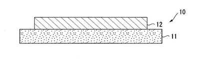
- the joined body according to the present embodiment is a power module substrate 10 in which a ceramic substrate 11 that is a ceramic member and a Cu plate 22 (circuit layer 12) that is a Cu member are joined.
- the power module 1 provided with the board
- the power module 1 includes a power module substrate 10 on which a circuit layer 12 is disposed, and a semiconductor element 3 bonded to one surface (the upper surface in FIG. 1) of the circuit layer 12 via a solder layer 2. ing.
- the power module substrate 10 includes a ceramic substrate 11 and a circuit layer 12 disposed on one surface (the upper surface in FIG. 2) of the ceramic substrate 11.
- the ceramic substrate 11 is made of ceramics such as AlN (aluminum nitride), Si 3 N 4 (silicon nitride), and Al 2 O 3 (alumina) having high insulating properties. In this embodiment, it is comprised with AlN (aluminum nitride) excellent in heat dissipation. Further, the thickness of the ceramic substrate 11 is set within a range of 0.2 to 1.5 mm, and in this embodiment is set to 0.635 mm.
- the circuit layer 12 is formed by bonding a conductive metal plate of Cu or Cu alloy to one surface of the ceramic substrate 11.
- the circuit layer 12 is formed by laminating a Cu-P brazing material 24, a Ti material 25, and a Cu plate 22 made of oxygen-free copper on one surface of the ceramic substrate 11, and heat-treating the ceramic substrate 11. It is formed by joining the Cu plate 22 (see FIG. 5).
- a Cu—P—Sn—Ni brazing material is used as the Cu—P brazing material 24.
- the ceramic substrate 11 side has a structure in which Sn is dissolved in Cu. Note that the thickness of the circuit layer 12 is set within a range of 0.1 mm or more and 1.0 mm or less, and is set to 0.2 mm in the present embodiment.
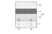
- FIG. 3 is a schematic cross-sectional explanatory view of the bonding layer 18 formed between the ceramic substrate 11 and the circuit layer 12.
- a Cu—Sn layer 14 is formed in the vicinity of the bonding surface of the ceramic substrate 11 in the bonding layer 18 between the ceramic substrate 11 and the circuit layer 12, and the Ti—Sn layer 14 has a Ti— A Ti-containing layer 15 containing is formed.
- the Cu—Sn layer 14 is a layer in which Sn is dissolved in Cu.
- the Cu—Sn layer 14 is a layer formed when P contained in the Cu—P brazing material 24 reacts with Ti of the Ti material 25 and is consumed.
- Examples of the Ti-containing layer 15 include a P—Ti intermetallic compound layer, a Ti layer, and a Cu—Ti intermetallic compound layer. The configuration of the Ti-containing layer 15 varies depending on the amount of Ti in the Ti material 25, bonding conditions, and the like.
- a Cu 3 P phase 16 is dispersed in the Cu—Sn layer 14, and this Cu 3 P phase 16 does not react with Ti of the Ti material 25 and remains in the Cu—P-based brazing material 24.
- P is produced by reacting with Cu.
- the semiconductor element 3 is made of a semiconductor material such as Si.
- the semiconductor element 3 and the circuit layer 12 are joined via the solder layer 2.
- the solder layer 2 is made of, for example, a Sn—Ag, Sn—In, or Sn—Ag—Cu solder material.
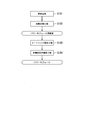
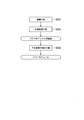
- a Cu—P brazing material 24, a Ti material 25, and a Cu plate 22 to be the circuit layer 12 are sequentially laminated on one surface of the ceramic substrate 11 (the upper surface in FIG. 5) ( Lamination process S01).
- this stacking step S01 Cu and Cu are interposed so that the atomic ratio [Ti / P] of P and Ti interposed between the ceramic substrate 11 and the Cu plate 22 is in the range of 0.1 to 0.8.
- -P-type brazing material 24 and Ti material 25 are arranged.
- the atomic ratio [Ti / P] of P and Ti interposed between the ceramic substrate 11 and the Cu plate 22 is less than 0.1, the amount of Ti that reacts with P becomes insufficient, and Cu A large amount of 3 P phase 16 is formed, and there is a possibility that the area ratio of the Cu 3 P phase in the region from the bonding surface of the ceramic substrate 11 to the circuit layer 12 side up to 50 ⁇ m cannot be made 15% or less.
- the atomic ratio [Ti / P] of P and Ti interposed between the ceramic substrate 11 and the Cu plate 22 exceeds 0.8, the liquid phase of the brazing material generated when heated is Ti Therefore, the melting point of the liquid phase rises and solidification easily proceeds.
- the atomic ratio [Ti / P] of P and Ti interposed between the ceramic substrate 11 and the Cu plate 22 is in the range of 0.1 to 0.8. It is set.
- the lower limit of the atomic ratio [Ti / P] of P and Ti interposed between the ceramic substrate 11 and the Cu plate 22 is 0.15 or more. It is preferable to set it to 0.2 or more.
- the upper limit of the atomic ratio [Ti / P] of P and Ti interposed between the ceramic substrate 11 and the Cu plate 22 is set to 0.7 or less. It is preferable to set it to 0.6 or less.
- the Ti material 25 is preferably formed by vapor deposition or sputtering when the thickness is from 0.1 ⁇ m to less than 1 ⁇ m, and a foil material is preferably used when the thickness is from 1 ⁇ m to 5 ⁇ m.
- the lower limit of the thickness of the Ti material 25 is preferably 0.2 ⁇ m or more, and more preferably 0.4 ⁇ m or more.
- the upper limit of the thickness of the Ti material 25 is preferably 3 ⁇ m or less, and more preferably 1.5 ⁇ m or less.
- the pressure in the vacuum heating furnace is in the range of 10 ⁇ 6 Pa to 10 ⁇ 3 Pa
- the heating temperature is in the range of 600 ° C. to 650 ° C.
- the heating time is 30 minutes or more. It is set within the range of 240 minutes or less.
- the rate of temperature increase up to the above heating temperature is in the range of 5 ° C./min to 30 ° C./min.
- the rate of temperature rise to the above heating temperature is set within a range of 5 ° C./min to 30 ° C./min.
- the lower limit of the heating rate up to the heating temperature is preferably 7 ° C./min or more, and more preferably 10 ° C./min or more. preferable.
- the upper limit of the heating rate to the heating temperature described above and below 25 ° C. / min further be 20 ° C. / min or less preferable.
- the Cu—P brazing material 24 is melted to form a liquid phase, the Ti material 25 is dissolved in the liquid phase, and the liquid phase is solidified. And are joined. At this time, P contained in the Cu—P brazing material 24 is bonded to Ti of the Ti material 25, and the Cu—Sn layer 14 is formed on the bonding surface side of the ceramic substrate 11. As a result, the circuit layer 12 is formed on one surface of the ceramic substrate 11, and the power module substrate 10 according to this embodiment is manufactured.
- the semiconductor element 3 is bonded to the upper surface of the circuit layer 12 of the power module substrate 10 via a solder material (semiconductor element bonding step S03). In this way, the power module 1 according to this embodiment is manufactured.
- the circuit layer extends from the bonding surface of the ceramic substrate 11. Since the area ratio of the Cu 3 P phase 16 in the region up to 50 ⁇ m toward the 12 side is set to 15% or less, the area occupied by the brittle Cu 3 P phase 16 in the bonding layer 18 is small. Even when a cooling cycle that reaches a high temperature is applied, the occurrence of partial discharge due to the Cu 3 P phase 16 on the circuit layer 12 side can be suppressed. Therefore, the power module substrate 10 according to the present embodiment is excellent in reliability when used in a high temperature environment.
- the ceramic substrate 11 and the Cu plate 22 are laminated in the laminating step S01 in which the ceramic substrate 11 and the Cu plate 22 that becomes the circuit layer 12 are laminated via the Cu—P brazing material 24 and the Ti material 25.
- the Cu—P brazing material 24 and the Ti material 25 are arranged so that the atomic ratio [Ti / P] of P and Ti intervening in between is 0.1 to 0.8. Therefore, the amount of Ti that reacts with P is secured, and unreacted P is reduced, so that formation of the Cu 3 P phase 16 can be suppressed. Therefore, the occurrence of partial discharge can be suppressed.
- the temperature increase rate to the heating temperature in the heat treatment step S02 is set to 5 ° C./min or more and 30 ° C./min or less, formation of the Cu 3 P phase 16 can be suppressed. Therefore, the occurrence of partial discharge can be suppressed.
- the pressure applied is 1 kgf / cm 2 or more, so that the liquid phase of the ceramic substrate 11 and the Cu—P brazing material 24 can be brought into close contact, and the ceramic substrate 11 and the Cu— -The Sn layer 14 can be bonded well. Moreover, since the pressurized pressure is set to 35 kgf / cm 2 or less, the occurrence of cracks in the ceramic substrate 11 can be suppressed.
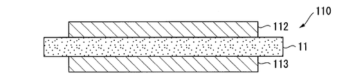
- FIG. 6 shows a power module 101 including the power module substrate 110 according to the second embodiment.
- the power module 101 includes a power module substrate 110 on which a circuit layer 112 and a metal layer 113 are disposed, and a semiconductor element bonded to one surface (upper surface in FIG. 6) of the circuit layer 112 via a solder layer 2. 3 and a heat sink 130 disposed on the other side of the metal layer 113 (lower side in FIG. 6).
- the power module substrate 110 includes a ceramic substrate 11, a circuit layer 112 disposed on one surface of the ceramic substrate 11 (upper surface in FIG. 7), and the other surface of the ceramic substrate 11. And a metal layer 113 disposed on the lower surface in FIG.
- the ceramic substrate 11 is made of AlN (aluminum nitride) with excellent heat dissipation.
- the circuit layer 112 is formed by sequentially laminating a Cu—P brazing material 124, a Ti material 25, and a Cu plate 122 made of oxygen-free copper on one surface of the ceramic substrate 11, and heat-treating them. It is formed by bonding a Cu plate 122 to the ceramic substrate 11 (see FIG. 10). Note that the thickness of the circuit layer 112 is set within a range of 0.1 mm or more and 1.0 mm or less, and is set to 0.2 mm in the present embodiment.
- the metal layer 113 is formed by bonding a Cu or Cu alloy metal plate to the other surface of the ceramic substrate 11 via a Cu—P brazing material 124.
- the metal layer 113 is formed by laminating a Cu-P brazing material 124, a Ti material 25, and a Cu plate 123 made of oxygen-free copper on the other surface of the ceramic substrate 11, and heat-treating it. It is formed by bonding a Cu plate 123 (see FIG. 10).
- the thickness of the metal layer 113 is set within a range of 0.1 mm or more and 1.0 mm or less, and is set to 0.15 mm in the present embodiment.
- a Cu—P—Sn—Ni brazing material is specifically used as the Cu—P brazing material 124.
- FIG. 8 is a schematic cross-sectional explanatory view of the bonding layer 118 between the ceramic substrate 11 and the circuit layer 112 and the metal layer 113.
- a Cu—Sn layer 14 is formed in the vicinity of the bonding surface of the ceramic substrate 11, and the circuit layer 112 side of this Cu—Sn layer 14 is formed.
- a Ti-containing layer 15 containing Ti is formed on the metal layer 113 side.
- the Cu 3 P phase 16 is dispersed in the Cu—Sn layer 14. In this Cu 3 P phase 16, the remaining P reacts with Cu without reacting with Ti of the Ti material 25. Generated by.
- the bonding surface of the ceramic substrate 11 is up to 50 ⁇ m from the bonding surface to the circuit layer 112 and the metal layer 113 side.
- the area ratio of the Cu 3 P phase in the region is 15% or less.
- the heat sink 130 dissipates heat from the power module substrate 110 described above.
- the heat sink 130 is made of Cu or Cu alloy, and in this embodiment is made of oxygen-free copper.
- the heat sink 130 is provided with a flow path 131 through which a cooling fluid flows.
- the heat sink 130 and the metal layer 113 are joined by a solder layer 132 made of a solder material.
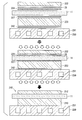
- a Cu—P brazing material 124, a Ti material 25, and a Cu plate 122 to be the circuit layer 112 are sequentially laminated on one surface (the upper surface in FIG. 10) of the ceramic substrate 11.
- the Cu—P brazing material 124, the Ti material 25, and the Cu plate 123 to be the metal layer 113 are sequentially laminated on the other surface (the lower surface in FIG. 10) of the ceramic substrate 11 (lamination step S101).
- the atomic ratio [Ti / P] of P and Ti interposed between the ceramic substrate 11 and the Cu plates 122 and 123 is in the range of 0.1 to 0.8.
- the Cu—P brazing material 124 and the Ti material 25 are disposed. Specifically, in consideration of the P content of the Cu—P brazing material 124 and the purity of the Ti material 25, by adjusting the thickness of the Cu—P brazing material 124 and the thickness of the Ti material 25, The atomic ratio [Ti / P] of P and Ti interposed between the ceramic substrate 11 and the Cu plate 22 is adjusted.
- the Cu plate 122, the Ti material 25, the Cu—P based brazing material 124, the ceramic substrate 11, the Cu—P based brazing material 124, the Ti material 25, and the Cu plate 123 are pressurized (pressure 1 kgf / In a state where it is not lower than cm 2 and not higher than 35 kgf / cm 2, it is placed in a vacuum heating furnace and heated to a temperature equal to or higher than the melting start temperature of the Cu—P brazing filler metal 124 (heat treatment step S102).
- the rate of temperature rise up to the above heating temperature is in the range of 5 ° C./min to 30 ° C./min.
- the Cu—P brazing material 124 melts to form a liquid phase, the Ti material 25 dissolves in this liquid phase, and the liquid phase solidifies, whereby the ceramic substrate 11 and the Cu plate 122 The ceramic substrate 11 and the Cu plate 123 are joined. At this time, P contained in the Cu—P based brazing material 124 is bonded to Ti of the Ti material 25, and the Cu—Sn layer 14 is formed on the ceramic substrate 11 side.
- the circuit layer 112 is formed on one surface of the ceramic substrate 11 and the metal layer 113 is formed on the other surface, and the power module substrate 110 according to this embodiment is manufactured.
- the heat sink 130 is bonded to the lower surface of the metal layer 113 of the power module substrate 110 via a solder material (heat sink bonding step S103).
- the semiconductor element 3 is bonded to the upper surface of the circuit layer 112 of the power module substrate 110 via a solder material (semiconductor element bonding step S104). In this way, the power module 101 according to this embodiment is manufactured.
- the ceramics in the bonding interface between the ceramic substrate 11 and the circuit layer 112 and in the bonding layer 118 between the ceramic substrate 11 and the metal layer 113 Since the area ratio of the Cu 3 P phase 16 in the region from the bonding surface of the substrate 11 to the circuit layer 112 side and the metal layer 113 side to 50 ⁇ m is 15% or less, the brittle Cu 3 P phase 16 in the bonding layer 118 is obtained. Even when a cooling cycle that reaches a relatively high temperature such as 200 ° C. or higher is loaded, the occurrence of partial discharge can be suppressed.
- the circuit layer 112 is bonded to one surface of the ceramic substrate 11 and the metal layer 113 is bonded to the other surface at the same time.
- the manufacturing process can be simplified and the manufacturing cost can be reduced.
- FIG. 11 shows a power module 201 including a power module substrate 210 according to the third embodiment.
- This power module 201 includes a power module substrate 210 on which a circuit layer 212 and a metal layer 213 are disposed, and a semiconductor element bonded to one surface (upper surface in FIG. 11) of the circuit layer 212 via a solder layer 2. 3 and a heat sink 230 bonded to the other side (lower side in FIG. 11) of the power module substrate 210.
- the power module substrate 210 includes a ceramic substrate 11, a circuit layer 212 disposed on one surface (the upper surface in FIG. 12) of the ceramic substrate 11, and the other surface of the ceramic substrate 11. And a metal layer 213 disposed on the lower surface in FIG.
- the ceramic substrate 11 is made of AlN (aluminum nitride) having excellent heat dissipation.
- the circuit layer 212 is obtained by laminating a Cu-P brazing material 224, a Ti material 25, and a Cu plate 222 made of oxygen-free copper on one surface of the ceramic substrate 11, and heat-treating the ceramic layer. It is formed by bonding a Cu plate 222 to the substrate 11 (see FIG. 15).
- the thickness of the circuit layer 212 is set within a range of 0.1 mm or more and 1.0 mm or less, and is set to 0.2 mm in the present embodiment.
- a Cu—P—Sn—Ni brazing material is specifically used as the Cu—P brazing material 224.
- FIG. 13 is a schematic cross-sectional explanatory view of the bonding layer 218 between the ceramic substrate 11 and the circuit layer 212.
- a Cu—Sn layer 14 is formed in the vicinity of the bonding surface of the ceramic substrate 11 in the bonding layer 218 between the ceramic substrate 11 and the circuit layer 212, and the Ti—Sn layer 14 has a Ti— A Ti-containing layer 15 containing is formed.
- the Cu 3 P phase 16 is dispersed in the Cu—Sn layer 14.
- the Cu 3 P phase 16 is generated by reacting P remaining without reacting with Ti of the Ti material 25 with Cu.
- the Cu 3 P phase 16 in the bonding layer 218 formed between the ceramic substrate 11 and the circuit layer 212 in the bonding layer 218 formed between the ceramic substrate 11 and the circuit layer 212, the Cu 3 P phase 16 in the region from the bonding surface of the ceramic substrate 11 to the circuit layer 212 side up to 50 ⁇ m.
- the area ratio is 15% or less.
- the metal layer 213 is formed by bonding an Al plate made of Al or an Al alloy to the other surface of the ceramic substrate 11.
- the metal layer 213 is formed by bonding an Al plate 223 having a purity of 99.99 mass% or more to the other surface of the ceramic substrate 11 (see FIG. 15).
- the Al plate 223 is bonded using a bonding material 227 made of an Al—Si brazing material.
- the thickness of the metal layer 213 is set within a range of 0.1 mm to 3.0 mm, and is set to 2.1 mm in the present embodiment.
- the heat sink 230 is made of Al or an Al alloy, and is made of A6063 (Al alloy) in the present embodiment.
- the heat sink 230 is provided with a flow path 231 through which a cooling fluid flows.
- the heat sink 230 and the metal layer 213 are bonded together by a bonding material 242 made of an Al—Si brazing material.
- a method for manufacturing the power module 201 according to the present embodiment will be described with reference to the flowchart of FIG. 14 and FIG.
- a Cu—P brazing material 224, a Ti material 25, and a Cu plate 222 to be a circuit layer 212 are sequentially laminated on one surface (the upper surface in FIG. 15) of the ceramic substrate 11.
- an Al plate 223 to be the metal layer 213 is sequentially laminated on the other surface (the lower surface in FIG. 15) of the ceramic substrate 11 with a bonding material 227 interposed therebetween.
- a heat sink 230 is laminated below the Al plate 223 via the bonding material 242 (lamination step S201).
- the Cu and Ti atomic ratio [Ti / P] interposed between the ceramic substrate 11 and the Cu plate 222 is within a range of 0.1 to 0.8.
- a P-type brazing material 224 and a Ti material 25 are disposed. Specifically, in consideration of the P content of the Cu—P brazing material 224 and the purity of the Ti material 25, by adjusting the thickness of the Cu—P brazing material 224 and the thickness of the Ti material 25, The atomic ratio [Ti / P] of P and Ti interposed between the ceramic substrate 11 and the Cu plate 222 is adjusted.
- the ceramic substrate 11, the Cu—P brazing material 224, the Ti material 25 and the Cu plate 222, the bonding material 227, the Al plate 223, the bonding material 242, and the heat sink 230 are pressurized in the stacking direction (pressure 1 to 35 kgf / pressure). cm 2 ), it is charged into a vacuum heating furnace and heated (heat treatment step S202).
- the pressure in the vacuum heating furnace is in the range of 10 ⁇ 6 Pa to 10 ⁇ 3 Pa
- the heating temperature is in the range of 600 ° C. to 650 ° C.
- the heating time is 30 minutes or more. It is set within the range of 240 minutes or less.
- the rate of temperature increase up to the above heating temperature is in the range of 5 ° C./min to 30 ° C./min.
- the Cu—P brazing material 224 is melted to form a liquid phase, the Ti material 25 is dissolved in the liquid phase, and the liquid phase is solidified, whereby the ceramic substrate 11 and the Cu plate 222 are formed. Are joined. At this time, P contained in the Cu—P based brazing material 224 is bonded to Ti of the Ti material 25, and the Cu—Sn layer 14 is formed on the ceramic substrate 11 side.
- the bonding material 227 is melted to form a liquid phase, and the liquid phase is solidified, whereby the ceramic substrate 11 and the Al plate 223 are bonded via the bonding material 227.
- the bonding material 242 is melted to form a liquid phase, and the liquid phase is solidified, whereby the Al plate 223 and the heat sink 230 are bonded via the bonding material 242.
- the power module substrate 210 and the power module substrate with a heat sink according to the present embodiment are manufactured.
- the semiconductor element 3 is bonded to the upper surface of the circuit layer 212 of the power module substrate 210 via a solder material (semiconductor element bonding step S203). In this way, the power module 201 according to this embodiment is manufactured.
- the power module substrate 210 according to the present embodiment configured as described above has the same effects as the power module substrate 10 described in the first embodiment. Further, in the power module substrate 210 according to the present embodiment, the metal layer 213 formed by bonding the Al plate 223 to the other surface of the ceramic substrate 11 is formed. It can be efficiently dissipated through the layer 213. Further, since Al has a relatively low deformation resistance, the thermal stress generated between the power module substrate 210 and the heat sink 230 is absorbed by the metal layer 213 when a cooling cycle is applied, and the ceramic substrate 11 is not cracked. Occurrence can be suppressed.
- the ceramic substrate 11 and the Cu plate 222 can be bonded at a relatively low temperature.
- the metal layer 213 made of the plate 223 can be bonded at the same time, so that the manufacturing process can be simplified and the manufacturing cost can be reduced.
- the power module is configured by mounting a semiconductor element on an insulating circuit board.
- the present invention is not limited to this.
- an LED module may be configured by mounting LED elements on a circuit layer of an insulated circuit board, or a thermoelectric module may be configured by mounting thermoelectric elements on a circuit layer of an insulated circuit board.
- the case where the circuit layer is bonded to one surface of the ceramic substrate and the metal layer is simultaneously bonded to the other surface has been described. However, the circuit layer and the metal layer are separately provided. You may join.
- the case where the circuit layer, the metal layer, and the heat sink are simultaneously bonded has been described. However, the circuit layer and the metal layer may be bonded to the ceramic substrate, and then the metal layer and the heat sink may be bonded. good.
- the case where the metal layer is bonded to the other surface of the ceramic substrate via the Al—Si brazing material has been described, but the bonding is performed by a transient liquid phase bonding method (TLP), Ag paste, or the like. May be.
- TLP transient liquid phase bonding method
- the heat sink provided with the flow path has been described in the second embodiment and the third embodiment, a plate-like thing called a heat radiating plate or a pin-like fin may be used.
- the power module substrate and the heat sink may be fixed by screwing or the like via grease.
- the heat sink may not be bonded to the other surface side of the power module substrate.
- a Ti foil may be used, or the Ti material may be formed by vapor deposition or sputtering.
- a Cu member / Ti clad material in which Ti is disposed on one surface of the Cu member can be used.
- a Ti material / brazing material clad material in which a Cu—P brazing material is disposed on one surface of the Ti material, and a Cu member / Ti material laminated in the order of a Cu member, a Ti material, and a Cu—P based brazing material. / Brazer cladding can be used.
- the Cu—P brazing material has been described as using a Cu—P—Sn—Ni brazing material, but other Cu—P brazing materials such as a Cu—P brazing material may be used. Good.
- a Cu—P brazing material suitable for the method for producing a joined body of the present invention will be described in detail.
- the content of P in the Cu—P brazing material is preferably 3 mass% or more and 10 mass% or less.
- P is an element having an effect of lowering the melting start temperature of the brazing material. Moreover, this P prevents oxidation of the brazing filler metal by covering the surface of the brazing filler metal with the P oxide generated by oxidation of P, and the surface of the molten brazing filler metal has good fluidity. It is an element having an effect of improving the wettability of the brazing material by covering. If the P content is less than 3 mass%, the effect of lowering the melting start temperature of the brazing material cannot be sufficiently obtained, the melting start temperature of the brazing material is increased, or the fluidity of the brazing material is insufficient.
- the bondability with the layer may decrease.
- the P content exceeds 10 mass%, a large amount of brittle intermetallic compounds are formed, and the bonding properties and bonding reliability between the ceramic substrate and the circuit layer may be reduced.
- the content of P contained in the Cu—P brazing material is preferably in the range of 3 mass% to 10 mass%.
- the Cu—P brazing material may contain Sn in an amount of 0.5 mass% to 25 mass%.
- Sn is an element having an effect of lowering the melting point of the brazing material.
- the Sn content is 0.5 mass% or more, the melting point of the brazing material can be reliably lowered. Further, when the Sn content is 25 mass% or less, the low temperature embrittlement of the brazing material can be suppressed, and the bonding reliability between the ceramic substrate and the circuit layer can be improved.
- the content is preferably in the range of 0.5 mass% to 25 mass%.
- the Cu—P brazing material may contain 2 mass% or more and 20 mass% or less of any one or more of Ni, Cr, Fe, and Mn.
- Ni, Cr, Fe, and Mn are elements having an effect of suppressing the formation of an intermetallic compound containing P at the interface between the ceramic substrate and the brazing material.
- the content of one or more of Ni, Cr, Fe, and Mn is 2 mass% or more, the formation of intermetallic compounds containing P at the bonding interface between the ceramic substrate and the brazing material is suppressed. This improves the bonding reliability between the ceramic substrate and the circuit layer.
- the content of any one or more of Ni, Cr, Fe, and Mn is 20 mass% or less, an increase in the melting start temperature of the brazing material is suppressed, and the fluidity of the brazing material is lowered. This can suppress this and improve the bondability between the ceramic substrate and the circuit layer.
- the content should be in the range of 2 mass% to 20 mass%. Is preferred.
- Example 1 Below, the result of the confirmation experiment (Example 1) conducted in order to confirm the effect of this invention is demonstrated.
- a Cu plate (37 mm ⁇ 37 mm ⁇ 0.2 mmt) made of Cu—P brazing material, Ti material and oxygen-free copper shown in Table 1 Laminate sequentially.
- the Cu—P-based brazing material and the Ti material were arranged so that the atomic ratio [Ti / P] of P and Ti interposed between the ceramic substrate and the Cu plate was the value shown in Table 1.
- the ceramic substrate used in this example was a ceramic substrate of ZrO 2 was added to sinter 10 mass% of AlN as 100 mass%.
- the ceramic substrate is heated by being charged in a vacuum heating furnace in a state of being pressurized at a pressure of 15 kgf / cm 2 in the laminating direction and heated at a temperature equal to or higher than the melting start temperature of the Cu—P brazing filler metal.
- a Cu plate was bonded to one surface to form a circuit layer.
- the heating temperature in this heat treatment step, the holding time at the heating temperature, and the rate of temperature rise to the heating temperature were carried out under the conditions shown in Table 1.
- the area ratio of the Cu 3 P phase in the vicinity of the ceramic substrate and the partial discharge characteristics in the bonding layer between the ceramic substrate and the circuit layer were evaluated.
- the obtained power module substrate was loaded with 100 cycles of a cooling cycle of 5 minutes at 200 ° C. and 5 minutes at ⁇ 40 ° C. Thereafter, a probe is applied to the surface of the circuit layer of the power module substrate and the side of the ceramic substrate where the circuit layer is not formed, immersed in 3M Fluorinert, and the measurement voltage is measured under the conditions specified in the international standard IEC61287. Was set to 3.3 kV, and the partial discharge characteristics were evaluated. Table 1 shows the measurement voltage evaluation results.
- Comparative Example 1-1 the atomic ratio [Ti / P] of P and Ti intervening between the ceramic substrate and the Cu plate is less than 0.1, and up to 50 ⁇ m from the bonding surface of the ceramic substrate to the Cu plate side. Since the area ratio of the Cu 3 P phase in the region exceeded 15%, the partial discharge characteristics were insufficient. In Comparative Example 1-2, the atomic ratio [Ti / P] of P and Ti interposed between the ceramic substrate and the Cu plate exceeded 0.8, and the partial discharge characteristics were insufficient.
- the rate of temperature increase to the heating temperature in the heat treatment step is less than 5 ° C./min, and the area of the Cu 3 P phase in the region from the bonding surface of the ceramic substrate to the Cu plate side to 50 ⁇ m. Since the rate exceeded 15%, the partial discharge characteristics were insufficient. In Comparative Example 1-4, the rate of temperature rise to the heating temperature in the heat treatment process exceeded 30 ° C./min, and the partial discharge characteristics were insufficient.
- Examples 1-1 to 1-8 of the present invention all had excellent partial discharge characteristics. According to Example 1, it was confirmed that partial discharge characteristics can be improved when a Cu plate is bonded to one surface of a ceramic substrate.
- Example 2 Next, the result of a confirmation experiment (Example 2) conducted to confirm the effect of the present invention will be described.
- a Cu plate (37 mm ⁇ 37 mm ⁇ 0) made of Cu—P brazing material, Ti material and oxygen-free copper shown in Table 2 .2 mmt) in order.
- the Cu—P based brazing material and the Ti material were arranged so that the atomic ratio [Ti / P] of P and Ti interposed between the ceramic substrate and the Cu plate was the numerical value shown in Table 2.
- the ceramic substrate used in this example was a ceramic substrate of ZrO 2 was added to sinter 10 mass% of AlN as 100 mass%.
- the ceramic substrate is heated by being charged in a vacuum heating furnace in a state of being pressurized at a pressure of 15 kgf / cm 2 in the laminating direction and heated at a temperature equal to or higher than the melting start temperature of the Cu—P brazing filler metal.
- a Cu plate was bonded to one surface and the other surface to form a circuit layer and a metal layer.
- the heating temperature in this heat treatment step, the holding time at the heating temperature, and the rate of temperature increase up to the heating temperature were carried out under the conditions shown in Table 2.
- Example 2 For the power module substrate obtained as described above, as in Example 1, the area ratio of the Cu 3 P phase in the vicinity of the ceramic substrate in the bonding layer between the ceramic substrate and the circuit layer, and the portion The discharge characteristics were evaluated. In evaluating the partial discharge characteristics, the probe was applied to the surface of the circuit layer and the metal layer. The evaluation results are shown in Table 2.
- Comparative Example 2-1 the atomic ratio [Ti / P] of P and Ti interposed between the ceramic substrate and the Cu plate is less than 0.1, and the distance from the bonding surface of the ceramic substrate to the Cu plate is up to 50 ⁇ m. Since the area ratio of the Cu 3 P phase in the region exceeded 15%, the partial discharge characteristics were insufficient. In Comparative Example 2-2, the atomic ratio [Ti / P] of P and Ti interposed between the ceramic substrate and the Cu plate exceeded 0.8, and the partial discharge characteristics were insufficient.
- the rate of temperature increase to the heating temperature in the heat treatment step is less than 5 ° C./min, and the area of the Cu 3 P phase in the region from the bonding surface of the ceramic substrate to the Cu plate side to 50 ⁇ m. Since the rate exceeded 15%, the partial discharge characteristics were insufficient. In Comparative Example 2-4, the rate of temperature rise to the heating temperature in the heat treatment process exceeded 30 ° C./min, and the partial discharge characteristics were insufficient.
- Examples 2-1 to 2-8 of the present invention were all excellent in partial discharge characteristics. According to Example 2, it was confirmed that partial discharge characteristics can be improved even when Cu plates are bonded to both surfaces of a ceramic substrate.
- Example 3 Next, the results of a confirmation experiment (Example 3) conducted to confirm the effect of the present invention will be described.
- the Al plate (37 mm ⁇ 37 mm ⁇ 2.1 mmt) made of Al having a purity of 99.99 mass% was laminated on the other surface of the ceramic substrate through an Al—Si brazing filler metal.
- the Cu—P-based brazing material and the Ti material were arranged so that the atomic ratio [Ti / P] of P and Ti interposed between the ceramic substrate and the Cu plate was the value shown in Table 3.
- the ceramic substrate used in this example was a ceramic substrate of ZrO 2 was added to sinter 10 mass% of AlN as 100 mass%.
- the pressure is 15 kgf / cm 2 in the laminating direction and charged in a vacuum heating furnace, the pressure is 10 ⁇ 6 Pa or more and 10 ⁇ 3 Pa or less, and the Cu—P brazing material is melted.
- a Cu plate was bonded to one surface of the ceramic substrate to form a circuit layer, and an Al plate was bonded to the other surface of the ceramic substrate to form a metal layer.
- the heating temperature in this heat treatment process, the holding time at the heating temperature, and the rate of temperature increase up to the heating temperature were carried out under the conditions shown in Table 3.
- Example 2 For the power module substrate obtained as described above, as in Example 1, the area ratio of the Cu 3 P phase in the vicinity of the ceramic substrate in the bonding layer between the ceramic substrate and the circuit layer, and the portion The discharge characteristics were evaluated. In evaluating the partial discharge characteristics, the probe was applied to the surface of the circuit layer and the metal layer. The evaluation results are shown in Table 3.
- Comparative Example 3-1 the atomic ratio [Ti / P] of P and Ti interposed between the ceramic substrate and the Cu plate is less than 0.1, and the distance from the bonding surface of the ceramic substrate to the Cu plate side is 50 ⁇ m. Since the area ratio of the Cu 3 P phase in the region exceeded 15%, the partial discharge characteristics were insufficient. In Comparative Example 3-2, the atomic ratio [Ti / P] of P and Ti interposed between the ceramic substrate and the Cu plate exceeded 0.8, and the partial discharge characteristics were insufficient.
- the rate of temperature increase to the heating temperature in the heat treatment step is less than 5 ° C./min, and the area of the Cu 3 P phase in the region from the bonding surface of the ceramic substrate to the Cu plate side to 50 ⁇ m. Since the rate exceeded 15%, the partial discharge characteristics were insufficient. In Comparative Example 3-4, the rate of temperature increase to the heating temperature in the heat treatment process exceeded 30 ° C./min, and the partial discharge characteristics were insufficient.
- Examples 3-1 to 3-8 of the present invention were all excellent in partial discharge characteristics.
- This Example 3 confirms that partial discharge characteristics can be improved even when a Cu plate is bonded to one surface of a ceramic substrate and an Al plate is bonded to the other surface of the ceramic substrate. It was.
- Example 4 Next, the results of a confirmation experiment (Example 4) conducted to confirm the effect of the present invention will be described.
- a ceramic substrate made of AlN 40 mm ⁇ 40 mm ⁇ 1.0 mmt
- a Cu plate 37 mm ⁇ 37 mm ⁇ 0
- the Cu—P-based brazing material and the Ti material were arranged so that the atomic ratio [Ti / P] of P and Ti interposed between the ceramic substrate and the Cu plate was the value shown in Table 4.
- the ceramic substrate used in this example was a ceramic substrate of ZrO 2 was added to sinter 10 mass% of AlN as 100 mass%.
- the ceramic substrate is heated by being charged in a vacuum heating furnace in a state of being pressurized at a pressure of 15 kgf / cm 2 in the laminating direction and heated at a temperature equal to or higher than the melting start temperature of the Cu—P brazing filler metal.
- a Cu plate was bonded to one surface and the other surface to form a circuit layer and a metal layer.
- the heating temperature in this heat treatment process, the holding time at the heating temperature, and the rate of temperature increase up to the heating temperature were carried out under the conditions shown in Table 4.
- the area ratio of the Cu 3 P phase in the vicinity of the ceramic substrate in the bonding layer between the ceramic substrate and the circuit layer was evaluated in the same manner as in Example 1.
- partial discharge characteristics first, 200 cycles of a cooling cycle of 15 minutes at 150 ° C. and 15 minutes at ⁇ 50 ° C. were loaded on the obtained power module substrate. After that, the probe is applied to the circuit layer surface and the metal layer surface of the power module substrate, immersed in Fluorinert, the discharge charge amount is set to 5.1 kV under the conditions specified in the international standard IEC61287, The discharge characteristics were evaluated. That is, in Example 4, the partial discharge characteristics at the time of high voltage load were evaluated. The evaluation results are shown in Table 4.
- Comparative Example 4-1 the atomic ratio [Ti / P] of P and Ti interposed between the ceramic substrate and the Cu plate is less than 0.1, and the distance from the bonding surface of the ceramic substrate to the Cu plate is up to 50 ⁇ m. Since the area ratio of the Cu 3 P phase in the region exceeded 15%, the partial discharge characteristics were insufficient. In Comparative Example 4-2, the atomic ratio [Ti / P] of P and Ti interposed between the ceramic substrate and the Cu plate exceeded 0.8, and the partial discharge characteristics were insufficient.
- the rate of temperature increase to the heating temperature in the heat treatment step is less than 5 ° C./min, and the area of the Cu 3 P phase in the region from the bonding surface of the ceramic substrate to the Cu plate side to 50 ⁇ m. Since the rate exceeded 15%, the partial discharge characteristics were insufficient. In Comparative Example 4-4, the rate of temperature rise to the heating temperature in the heat treatment process exceeded 30 ° C./min, and the partial discharge characteristics were insufficient.
- Examples 4-1 to 4-8 of the present invention were all excellent in partial discharge characteristics. According to Example 4, it was confirmed that sufficient partial discharge characteristics could be obtained even when the measurement voltage was set as high as 5.1 Kv.
- Example 5 Next, the results of a confirmation experiment (Example 5) conducted to confirm the effect of the present invention will be described.
- a Cu plate made of Cu—P brazing material, Ti material and oxygen-free copper shown in Table 5 37 mm ⁇ 37 mm ⁇ 0.2 mmt.
- the Cu—P-based brazing material and the Ti material were arranged so that the atomic ratio [Ti / P] of P and Ti interposed between the ceramic substrate and the Cu plate was the value shown in Table 5. .
- the ceramic substrate is heated by being charged in a vacuum heating furnace in a state of being pressurized at a pressure of 15 kgf / cm 2 in the laminating direction and heated at a temperature equal to or higher than the melting start temperature of the Cu—P brazing filler metal.
- a Cu plate was bonded to one surface and the other surface to form a circuit layer and a metal layer.
- the heating temperature in this heat treatment process, the holding time at the heating temperature, and the rate of temperature increase up to the heating temperature were carried out under the conditions shown in Table 5.
- Example 2 For the power module substrate obtained as described above, as in Example 1, the area ratio of the Cu 3 P phase in the vicinity of the ceramic substrate in the bonding layer between the ceramic substrate and the circuit layer, and the portion The discharge characteristics were evaluated. In evaluating the partial discharge characteristics, the probe was applied to the surface of the circuit layer and the metal layer. The evaluation results are shown in Table 5.
- Comparative Example 5-1 the atomic ratio [Ti / P] of P and Ti interposed between the ceramic substrate and the Cu plate is less than 0.1, and the distance from the bonding surface of the ceramic substrate to the Cu plate side is up to 50 ⁇ m. Since the area ratio of the Cu 3 P phase in the region exceeded 15%, the partial discharge characteristics were insufficient. In Comparative Example 5-2, the atomic ratio [Ti / P] of P and Ti interposed between the ceramic substrate and the Cu plate exceeded 0.8, and the partial discharge characteristics were insufficient.
- the rate of temperature rise to the heating temperature in the heat treatment step is less than 5 ° C./min, and the area of the Cu 3 P phase in the region from the bonding surface of the ceramic substrate to the Cu plate side to 50 ⁇ m. Since the rate exceeded 15%, the partial discharge characteristics were insufficient. In Comparative Example 5-4, the rate of temperature rise to the heating temperature in the heat treatment process exceeded 30 ° C./min, and the partial discharge characteristics were insufficient.
- Examples 5-1 to 5-8 of the present invention were all excellent in partial discharge characteristics. According to Example 5, it was confirmed that partial discharge characteristics can be improved even when Cu plates are bonded to both surfaces of a ceramic substrate made of Si 3 N 4 .
- the power module substrate comprising the joined body, the power module, the method for producing the joined body, and the method for producing the power module substrate, the ceramic member and the Cu member are satisfactorily joined.
- a cooling cycle that reaches a relatively high temperature is loaded, it is possible to suppress the occurrence of partial discharge.
Landscapes
- Engineering & Computer Science (AREA)
- Chemical & Material Sciences (AREA)
- Ceramic Engineering (AREA)
- Mechanical Engineering (AREA)
- Materials Engineering (AREA)
- Organic Chemistry (AREA)
- Manufacturing & Machinery (AREA)
- Structural Engineering (AREA)
- Metallurgy (AREA)
- Inorganic Chemistry (AREA)
- Cooling Or The Like Of Semiconductors Or Solid State Devices (AREA)
- Ceramic Products (AREA)
Abstract
Priority Applications (5)
| Application Number | Priority Date | Filing Date | Title |
|---|---|---|---|
| EP17741530.4A EP3407381B1 (fr) | 2016-01-22 | 2017-01-20 | Corps lié ainsi que procédé de fabrication de celui-ci, substrat pour module de puissance ainsi que procédé de fabrication de celui-ci, et module de puissance |
| US16/070,339 US11393738B2 (en) | 2016-01-22 | 2017-01-20 | Bonded body, power module substrate, power module, method for manufacturing bonded body, and method for manufacturing power module substrate |
| CN201780015338.6A CN108701659B (zh) | 2016-01-22 | 2017-01-20 | 接合体、功率模块用基板、功率模块、接合体的制造方法及功率模块用基板的制造方法 |
| KR1020187023510A KR102524698B1 (ko) | 2016-01-22 | 2017-01-20 | 접합체, 파워 모듈용 기판, 파워 모듈, 접합체의 제조 방법 및 파워 모듈용 기판의 제조 방법 |
| US17/742,044 US12199006B2 (en) | 2016-01-22 | 2022-05-11 | Bonded body, power module substrate, power module, method for manufacturing bonded body, and method for manufacturing power module substrate |
Applications Claiming Priority (4)
| Application Number | Priority Date | Filing Date | Title |
|---|---|---|---|
| JP2016-010676 | 2016-01-22 | ||
| JP2016010676 | 2016-01-22 | ||
| JP2017-000417 | 2017-01-05 | ||
| JP2017000417A JP2017135374A (ja) | 2016-01-22 | 2017-01-05 | 接合体、パワーモジュール用基板、パワーモジュール、接合体の製造方法及びパワーモジュール用基板の製造方法 |
Related Child Applications (2)
| Application Number | Title | Priority Date | Filing Date |
|---|---|---|---|
| US16/070,339 A-371-Of-International US11393738B2 (en) | 2016-01-22 | 2017-01-20 | Bonded body, power module substrate, power module, method for manufacturing bonded body, and method for manufacturing power module substrate |
| US17/742,044 Division US12199006B2 (en) | 2016-01-22 | 2022-05-11 | Bonded body, power module substrate, power module, method for manufacturing bonded body, and method for manufacturing power module substrate |
Publications (1)
| Publication Number | Publication Date |
|---|---|
| WO2017126653A1 true WO2017126653A1 (fr) | 2017-07-27 |
Family
ID=59362046
Family Applications (1)
| Application Number | Title | Priority Date | Filing Date |
|---|---|---|---|
| PCT/JP2017/001922 Ceased WO2017126653A1 (fr) | 2016-01-22 | 2017-01-20 | Corps lié ainsi que procédé de fabrication de celui-ci, substrat pour module de puissance ainsi que procédé de fabrication de celui-ci, et module de puissance |
Country Status (4)
| Country | Link |
|---|---|
| US (1) | US12199006B2 (fr) |
| EP (1) | EP3407381B1 (fr) |
| CN (1) | CN108701659B (fr) |
| WO (1) | WO2017126653A1 (fr) |
Cited By (1)
| Publication number | Priority date | Publication date | Assignee | Title |
|---|---|---|---|---|
| DE102019126954A1 (de) * | 2019-10-08 | 2021-04-08 | Rogers Germany Gmbh | Verfahren zur Herstellung eines Metall-Keramik-Substrats, Lötsystem und Metall-Keramik-Substrat, hergestellt mit einem solchen Verfahren |
Families Citing this family (1)
| Publication number | Priority date | Publication date | Assignee | Title |
|---|---|---|---|---|
| DE102019135099A1 (de) * | 2019-12-19 | 2021-06-24 | Rogers Germany Gmbh | Verfahren zur Herstellung eines Metall-Keramik-Substrats und Metall-Keramik-Substrat, hergestellt mit einem solchen Verfahren |
Citations (5)
| Publication number | Priority date | Publication date | Assignee | Title |
|---|---|---|---|---|
| JP2008181940A (ja) * | 2007-01-23 | 2008-08-07 | Mitsubishi Materials Corp | パワーモジュール用基板の製造方法およびパワーモジュール用基板並びにパワーモジュール |
| JP4375730B2 (ja) | 2004-04-23 | 2009-12-02 | 本田技研工業株式会社 | 銅とセラミックス又は炭素基銅複合材料との接合用ろう材及び同接合方法 |
| JP2015043392A (ja) | 2013-08-26 | 2015-03-05 | 三菱マテリアル株式会社 | 接合体及びパワーモジュール用基板 |
| JP2015043393A (ja) | 2013-08-26 | 2015-03-05 | 三菱マテリアル株式会社 | 接合体の製造方法及びパワーモジュール用基板の製造方法 |
| JP2015065423A (ja) | 2013-08-26 | 2015-04-09 | 三菱マテリアル株式会社 | 接合体及びパワーモジュール用基板 |
Family Cites Families (11)
| Publication number | Priority date | Publication date | Assignee | Title |
|---|---|---|---|---|
| EP0480038B1 (fr) | 1990-04-16 | 1997-07-09 | Denki Kagaku Kogyo Kabushiki Kaisha | Carte a circuits en ceramique |
| JP4077888B2 (ja) * | 1995-07-21 | 2008-04-23 | 株式会社東芝 | セラミックス回路基板 |
| US6033787A (en) | 1996-08-22 | 2000-03-07 | Mitsubishi Materials Corporation | Ceramic circuit board with heat sink |
| JP3682552B2 (ja) | 1997-03-12 | 2005-08-10 | 同和鉱業株式会社 | 金属−セラミックス複合基板の製造方法 |
| CA2410636A1 (fr) * | 2000-05-24 | 2001-11-29 | Stephen F. Corbin | Soudures et brasures a point de fusion variable |
| JP2003101184A (ja) | 2001-09-27 | 2003-04-04 | Kyocera Corp | セラミック回路基板およびその製造方法 |
| JP5492191B2 (ja) | 2009-03-30 | 2014-05-14 | 株式会社トクヤマ | メタライズド基板を製造する方法、メタライズド基板 |
| WO2013002407A1 (fr) | 2011-06-30 | 2013-01-03 | 日立金属株式会社 | Métal d'apport de brasage, pâte métallique d'apport de brasage, substrat pour circuit céramique, substrat pour circuit maître céramique, et module d'alimentation à semi-conducteurs |
| EP2811513B1 (fr) * | 2012-02-01 | 2019-12-18 | Mitsubishi Materials Corporation | Procédé de fabrication de substrat pour modules de courant |
| JP6565527B2 (ja) | 2014-09-30 | 2019-08-28 | 三菱マテリアル株式会社 | Ag下地層付パワーモジュール用基板及びパワーモジュール |
| US10307861B2 (en) * | 2014-12-27 | 2019-06-04 | Cooler Master Corp. | Bonded aluminum-dissimilar metal structure and method of making same |
-
2017
- 2017-01-20 WO PCT/JP2017/001922 patent/WO2017126653A1/fr not_active Ceased
- 2017-01-20 EP EP17741530.4A patent/EP3407381B1/fr active Active
- 2017-01-20 CN CN201780015338.6A patent/CN108701659B/zh active Active
-
2022
- 2022-05-11 US US17/742,044 patent/US12199006B2/en active Active
Patent Citations (5)
| Publication number | Priority date | Publication date | Assignee | Title |
|---|---|---|---|---|
| JP4375730B2 (ja) | 2004-04-23 | 2009-12-02 | 本田技研工業株式会社 | 銅とセラミックス又は炭素基銅複合材料との接合用ろう材及び同接合方法 |
| JP2008181940A (ja) * | 2007-01-23 | 2008-08-07 | Mitsubishi Materials Corp | パワーモジュール用基板の製造方法およびパワーモジュール用基板並びにパワーモジュール |
| JP2015043392A (ja) | 2013-08-26 | 2015-03-05 | 三菱マテリアル株式会社 | 接合体及びパワーモジュール用基板 |
| JP2015043393A (ja) | 2013-08-26 | 2015-03-05 | 三菱マテリアル株式会社 | 接合体の製造方法及びパワーモジュール用基板の製造方法 |
| JP2015065423A (ja) | 2013-08-26 | 2015-04-09 | 三菱マテリアル株式会社 | 接合体及びパワーモジュール用基板 |
Non-Patent Citations (1)
| Title |
|---|
| See also references of EP3407381A4 |
Cited By (4)
| Publication number | Priority date | Publication date | Assignee | Title |
|---|---|---|---|---|
| DE102019126954A1 (de) * | 2019-10-08 | 2021-04-08 | Rogers Germany Gmbh | Verfahren zur Herstellung eines Metall-Keramik-Substrats, Lötsystem und Metall-Keramik-Substrat, hergestellt mit einem solchen Verfahren |
| WO2021069320A1 (fr) | 2019-10-08 | 2021-04-15 | Rogers Germany Gmbh | Procédé de fabrication d'un substrat métal-céramique, système de brasure et substrat métal-céramique produit par un tel procédé |
| DE202020005466U1 (de) | 2019-10-08 | 2021-06-09 | Rogers Germany Gmbh | Lötsystem und Metall-Keramik-Substrat, hergestellt mit einem solchen Verfahren |
| DE102019126954B4 (de) | 2019-10-08 | 2024-12-05 | Rogers Germany Gmbh | Verfahren zur Herstellung eines Metall-Keramik-Substrats, Lötsystem und Metall-Keramik-Substrat, hergestellt mit einem solchen Verfahren |
Also Published As
| Publication number | Publication date |
|---|---|
| CN108701659B (zh) | 2022-05-13 |
| CN108701659A (zh) | 2018-10-23 |
| US20220278019A1 (en) | 2022-09-01 |
| US12199006B2 (en) | 2025-01-14 |
| EP3407381A1 (fr) | 2018-11-28 |
| EP3407381A4 (fr) | 2019-08-21 |
| EP3407381B1 (fr) | 2022-02-23 |
Similar Documents
| Publication | Publication Date | Title |
|---|---|---|
| JP6079505B2 (ja) | 接合体及びパワーモジュール用基板 | |
| JP6111764B2 (ja) | パワーモジュール用基板の製造方法 | |
| JP5614485B2 (ja) | ヒートシンク付パワーモジュール用基板、ヒートシンク付パワーモジュール、及びヒートシンク付パワーモジュール用基板の製造方法 | |
| JP6127833B2 (ja) | 接合体の製造方法及びパワーモジュール用基板の製造方法 | |
| KR102422064B1 (ko) | 접합체, 히트 싱크가 부착된 파워 모듈용 기판, 히트 싱크, 및 접합체의 제조 방법, 히트 싱크가 부착된 파워 모듈용 기판의 제조 방법, 히트 싱크의 제조 방법 | |
| KR102300413B1 (ko) | 접합체, 파워 모듈용 기판, 파워 모듈 및 접합체의 제조 방법 | |
| JP6687109B2 (ja) | パワーモジュール用基板 | |
| JP5720839B2 (ja) | 接合体及びパワーモジュール用基板 | |
| JP2014060216A (ja) | ヒートシンク付パワーモジュール用基板、ヒートシンク付パワーモジュール、及びヒートシンク付パワーモジュール用基板の製造方法 | |
| KR102524698B1 (ko) | 접합체, 파워 모듈용 기판, 파워 모듈, 접합체의 제조 방법 및 파워 모듈용 기판의 제조 방법 | |
| JP6819299B2 (ja) | 接合体、パワーモジュール用基板、接合体の製造方法及びパワーモジュール用基板の製造方法 | |
| US12199006B2 (en) | Bonded body, power module substrate, power module, method for manufacturing bonded body, and method for manufacturing power module substrate | |
| JP6323103B2 (ja) | パワーモジュール用基板及びヒートシンク付パワーモジュール用基板 | |
| JP4635715B2 (ja) | はんだ合金およびそれを用いた半導体装置 | |
| CN109075135B (zh) | 接合体、功率模块用基板、接合体的制造方法及功率模块用基板的制造方法 | |
| WO2016167217A1 (fr) | Corps lié, substrat pour module d'alimentation pourvu d'un dissipateur thermique, dissipateur thermique, procédé de fabrication de corps lié, procédé de fabrication de substrat pour module d'alimentation pourvu d'un dissipateur thermique, et procédé de fabrication de dissipateur thermique |
Legal Events
| Date | Code | Title | Description |
|---|---|---|---|
| 121 | Ep: the epo has been informed by wipo that ep was designated in this application |
Ref document number: 17741530 Country of ref document: EP Kind code of ref document: A1 |
|
| NENP | Non-entry into the national phase |
Ref country code: DE |
|
| ENP | Entry into the national phase |
Ref document number: 20187023510 Country of ref document: KR Kind code of ref document: A |
|
| WWE | Wipo information: entry into national phase |
Ref document number: 1020187023510 Country of ref document: KR |
|
| WWE | Wipo information: entry into national phase |
Ref document number: 2017741530 Country of ref document: EP |
|
| ENP | Entry into the national phase |
Ref document number: 2017741530 Country of ref document: EP Effective date: 20180822 |