WO2017130420A1 - 半導体モジュール - Google Patents
半導体モジュール Download PDFInfo
- Publication number
- WO2017130420A1 WO2017130420A1 PCT/JP2016/052842 JP2016052842W WO2017130420A1 WO 2017130420 A1 WO2017130420 A1 WO 2017130420A1 JP 2016052842 W JP2016052842 W JP 2016052842W WO 2017130420 A1 WO2017130420 A1 WO 2017130420A1
- Authority
- WO
- WIPO (PCT)
- Prior art keywords
- semiconductor module
- power device
- electrode
- conductor layer
- substrate
- Prior art date
- Legal status (The legal status is an assumption and is not a legal conclusion. Google has not performed a legal analysis and makes no representation as to the accuracy of the status listed.)
- Ceased
Links
Images


Classifications
-
- H—ELECTRICITY
- H10—SEMICONDUCTOR DEVICES; ELECTRIC SOLID-STATE DEVICES NOT OTHERWISE PROVIDED FOR
- H10W—GENERIC PACKAGES, INTERCONNECTIONS, CONNECTORS OR OTHER CONSTRUCTIONAL DETAILS OF DEVICES COVERED BY CLASS H10
- H10W90/00—Package configurations
-
- H—ELECTRICITY
- H10—SEMICONDUCTOR DEVICES; ELECTRIC SOLID-STATE DEVICES NOT OTHERWISE PROVIDED FOR
- H10W—GENERIC PACKAGES, INTERCONNECTIONS, CONNECTORS OR OTHER CONSTRUCTIONAL DETAILS OF DEVICES COVERED BY CLASS H10
- H10W40/00—Arrangements for thermal protection or thermal control
- H10W40/20—Arrangements for cooling
- H10W40/22—Arrangements for cooling characterised by their shape, e.g. having conical or cylindrical projections
-
- H—ELECTRICITY
- H10—SEMICONDUCTOR DEVICES; ELECTRIC SOLID-STATE DEVICES NOT OTHERWISE PROVIDED FOR
- H10W—GENERIC PACKAGES, INTERCONNECTIONS, CONNECTORS OR OTHER CONSTRUCTIONAL DETAILS OF DEVICES COVERED BY CLASS H10
- H10W40/00—Arrangements for thermal protection or thermal control
- H10W40/20—Arrangements for cooling
- H10W40/25—Arrangements for cooling characterised by their materials
- H10W40/255—Arrangements for cooling characterised by their materials having a laminate or multilayered structure, e.g. direct bond copper [DBC] ceramic substrates
-
- H—ELECTRICITY
- H10—SEMICONDUCTOR DEVICES; ELECTRIC SOLID-STATE DEVICES NOT OTHERWISE PROVIDED FOR
- H10W—GENERIC PACKAGES, INTERCONNECTIONS, CONNECTORS OR OTHER CONSTRUCTIONAL DETAILS OF DEVICES COVERED BY CLASS H10
- H10W40/00—Arrangements for thermal protection or thermal control
- H10W40/70—Fillings or auxiliary members in containers or in encapsulations for thermal protection or control
- H10W40/77—Auxiliary members characterised by their shape
- H10W40/778—Auxiliary members characterised by their shape in encapsulations
-
- H—ELECTRICITY
- H10—SEMICONDUCTOR DEVICES; ELECTRIC SOLID-STATE DEVICES NOT OTHERWISE PROVIDED FOR
- H10W—GENERIC PACKAGES, INTERCONNECTIONS, CONNECTORS OR OTHER CONSTRUCTIONAL DETAILS OF DEVICES COVERED BY CLASS H10
- H10W42/00—Arrangements for protection of devices
- H10W42/60—Arrangements for protection of devices protecting against electrostatic charges or discharges, e.g. Faraday shields
-
- H—ELECTRICITY
- H10—SEMICONDUCTOR DEVICES; ELECTRIC SOLID-STATE DEVICES NOT OTHERWISE PROVIDED FOR
- H10W—GENERIC PACKAGES, INTERCONNECTIONS, CONNECTORS OR OTHER CONSTRUCTIONAL DETAILS OF DEVICES COVERED BY CLASS H10
- H10W70/00—Package substrates; Interposers; Redistribution layers [RDL]
- H10W70/60—Insulating or insulated package substrates; Interposers; Redistribution layers
- H10W70/62—Insulating or insulated package substrates; Interposers; Redistribution layers characterised by their interconnections
- H10W70/63—Vias, e.g. via plugs
- H10W70/635—Through-vias
-
- H—ELECTRICITY
- H10—SEMICONDUCTOR DEVICES; ELECTRIC SOLID-STATE DEVICES NOT OTHERWISE PROVIDED FOR
- H10W—GENERIC PACKAGES, INTERCONNECTIONS, CONNECTORS OR OTHER CONSTRUCTIONAL DETAILS OF DEVICES COVERED BY CLASS H10
- H10W72/00—Interconnections or connectors in packages
-
- H—ELECTRICITY
- H10—SEMICONDUCTOR DEVICES; ELECTRIC SOLID-STATE DEVICES NOT OTHERWISE PROVIDED FOR
- H10W—GENERIC PACKAGES, INTERCONNECTIONS, CONNECTORS OR OTHER CONSTRUCTIONAL DETAILS OF DEVICES COVERED BY CLASS H10
- H10W74/00—Encapsulations, e.g. protective coatings
- H10W74/10—Encapsulations, e.g. protective coatings characterised by their shape or disposition
- H10W74/111—Encapsulations, e.g. protective coatings characterised by their shape or disposition the semiconductor body being completely enclosed
- H10W74/114—Encapsulations, e.g. protective coatings characterised by their shape or disposition the semiconductor body being completely enclosed by a substrate and the encapsulations
-
- H—ELECTRICITY
- H10—SEMICONDUCTOR DEVICES; ELECTRIC SOLID-STATE DEVICES NOT OTHERWISE PROVIDED FOR
- H10W—GENERIC PACKAGES, INTERCONNECTIONS, CONNECTORS OR OTHER CONSTRUCTIONAL DETAILS OF DEVICES COVERED BY CLASS H10
- H10W74/00—Encapsulations, e.g. protective coatings
- H10W74/10—Encapsulations, e.g. protective coatings characterised by their shape or disposition
- H10W74/111—Encapsulations, e.g. protective coatings characterised by their shape or disposition the semiconductor body being completely enclosed
- H10W74/121—Encapsulations, e.g. protective coatings characterised by their shape or disposition the semiconductor body being completely enclosed by multiple encapsulations, e.g. by a thin protective coating and a thick encapsulation
-
- H—ELECTRICITY
- H10—SEMICONDUCTOR DEVICES; ELECTRIC SOLID-STATE DEVICES NOT OTHERWISE PROVIDED FOR
- H10W—GENERIC PACKAGES, INTERCONNECTIONS, CONNECTORS OR OTHER CONSTRUCTIONAL DETAILS OF DEVICES COVERED BY CLASS H10
- H10W74/00—Encapsulations, e.g. protective coatings
- H10W74/40—Encapsulations, e.g. protective coatings characterised by their materials
-
- H—ELECTRICITY
- H10—SEMICONDUCTOR DEVICES; ELECTRIC SOLID-STATE DEVICES NOT OTHERWISE PROVIDED FOR
- H10W—GENERIC PACKAGES, INTERCONNECTIONS, CONNECTORS OR OTHER CONSTRUCTIONAL DETAILS OF DEVICES COVERED BY CLASS H10
- H10W76/00—Containers; Fillings or auxiliary members therefor; Seals
- H10W76/10—Containers or parts thereof
- H10W76/12—Containers or parts thereof characterised by their shape
- H10W76/15—Containers comprising an insulating or insulated base
-
- H—ELECTRICITY
- H10—SEMICONDUCTOR DEVICES; ELECTRIC SOLID-STATE DEVICES NOT OTHERWISE PROVIDED FOR
- H10W—GENERIC PACKAGES, INTERCONNECTIONS, CONNECTORS OR OTHER CONSTRUCTIONAL DETAILS OF DEVICES COVERED BY CLASS H10
- H10W76/00—Containers; Fillings or auxiliary members therefor; Seals
- H10W76/40—Fillings or auxiliary members in containers, e.g. centering rings
- H10W76/42—Fillings
- H10W76/47—Solid or gel fillings
-
- H—ELECTRICITY
- H10—SEMICONDUCTOR DEVICES; ELECTRIC SOLID-STATE DEVICES NOT OTHERWISE PROVIDED FOR
- H10W—GENERIC PACKAGES, INTERCONNECTIONS, CONNECTORS OR OTHER CONSTRUCTIONAL DETAILS OF DEVICES COVERED BY CLASS H10
- H10W76/00—Containers; Fillings or auxiliary members therefor; Seals
- H10W76/60—Seals
-
- H—ELECTRICITY
- H10—SEMICONDUCTOR DEVICES; ELECTRIC SOLID-STATE DEVICES NOT OTHERWISE PROVIDED FOR
- H10W—GENERIC PACKAGES, INTERCONNECTIONS, CONNECTORS OR OTHER CONSTRUCTIONAL DETAILS OF DEVICES COVERED BY CLASS H10
- H10W90/00—Package configurations
- H10W90/401—Package configurations characterised by multiple insulating or insulated package substrates, interposers or RDLs
-
- H—ELECTRICITY
- H10—SEMICONDUCTOR DEVICES; ELECTRIC SOLID-STATE DEVICES NOT OTHERWISE PROVIDED FOR
- H10W—GENERIC PACKAGES, INTERCONNECTIONS, CONNECTORS OR OTHER CONSTRUCTIONAL DETAILS OF DEVICES COVERED BY CLASS H10
- H10W72/00—Interconnections or connectors in packages
- H10W72/071—Connecting or disconnecting
- H10W72/073—Connecting or disconnecting of die-attach connectors
- H10W72/07331—Connecting techniques
- H10W72/07336—Soldering or alloying
-
- H—ELECTRICITY
- H10—SEMICONDUCTOR DEVICES; ELECTRIC SOLID-STATE DEVICES NOT OTHERWISE PROVIDED FOR
- H10W—GENERIC PACKAGES, INTERCONNECTIONS, CONNECTORS OR OTHER CONSTRUCTIONAL DETAILS OF DEVICES COVERED BY CLASS H10
- H10W72/00—Interconnections or connectors in packages
- H10W72/071—Connecting or disconnecting
- H10W72/073—Connecting or disconnecting of die-attach connectors
- H10W72/07351—Connecting or disconnecting of die-attach connectors characterised by changes in properties of the die-attach connectors during connecting
- H10W72/07354—Connecting or disconnecting of die-attach connectors characterised by changes in properties of the die-attach connectors during connecting changes in dispositions
-
- H—ELECTRICITY
- H10—SEMICONDUCTOR DEVICES; ELECTRIC SOLID-STATE DEVICES NOT OTHERWISE PROVIDED FOR
- H10W—GENERIC PACKAGES, INTERCONNECTIONS, CONNECTORS OR OTHER CONSTRUCTIONAL DETAILS OF DEVICES COVERED BY CLASS H10
- H10W72/00—Interconnections or connectors in packages
- H10W72/30—Die-attach connectors
- H10W72/341—Dispositions of die-attach connectors, e.g. layouts
- H10W72/347—Dispositions of multiple die-attach connectors
-
- H—ELECTRICITY
- H10—SEMICONDUCTOR DEVICES; ELECTRIC SOLID-STATE DEVICES NOT OTHERWISE PROVIDED FOR
- H10W—GENERIC PACKAGES, INTERCONNECTIONS, CONNECTORS OR OTHER CONSTRUCTIONAL DETAILS OF DEVICES COVERED BY CLASS H10
- H10W72/00—Interconnections or connectors in packages
- H10W72/30—Die-attach connectors
- H10W72/351—Materials of die-attach connectors
- H10W72/352—Materials of die-attach connectors comprising metals or metalloids, e.g. solders
-
- H—ELECTRICITY
- H10—SEMICONDUCTOR DEVICES; ELECTRIC SOLID-STATE DEVICES NOT OTHERWISE PROVIDED FOR
- H10W—GENERIC PACKAGES, INTERCONNECTIONS, CONNECTORS OR OTHER CONSTRUCTIONAL DETAILS OF DEVICES COVERED BY CLASS H10
- H10W72/00—Interconnections or connectors in packages
- H10W72/30—Die-attach connectors
- H10W72/381—Auxiliary members
-
- H—ELECTRICITY
- H10—SEMICONDUCTOR DEVICES; ELECTRIC SOLID-STATE DEVICES NOT OTHERWISE PROVIDED FOR
- H10W—GENERIC PACKAGES, INTERCONNECTIONS, CONNECTORS OR OTHER CONSTRUCTIONAL DETAILS OF DEVICES COVERED BY CLASS H10
- H10W72/00—Interconnections or connectors in packages
- H10W72/50—Bond wires
- H10W72/541—Dispositions of bond wires
- H10W72/5445—Dispositions of bond wires being orthogonal to a side surface of the chip, e.g. parallel arrangements
-
- H—ELECTRICITY
- H10—SEMICONDUCTOR DEVICES; ELECTRIC SOLID-STATE DEVICES NOT OTHERWISE PROVIDED FOR
- H10W—GENERIC PACKAGES, INTERCONNECTIONS, CONNECTORS OR OTHER CONSTRUCTIONAL DETAILS OF DEVICES COVERED BY CLASS H10
- H10W72/00—Interconnections or connectors in packages
- H10W72/50—Bond wires
- H10W72/551—Materials of bond wires
- H10W72/552—Materials of bond wires comprising metals or metalloids, e.g. silver
-
- H—ELECTRICITY
- H10—SEMICONDUCTOR DEVICES; ELECTRIC SOLID-STATE DEVICES NOT OTHERWISE PROVIDED FOR
- H10W—GENERIC PACKAGES, INTERCONNECTIONS, CONNECTORS OR OTHER CONSTRUCTIONAL DETAILS OF DEVICES COVERED BY CLASS H10
- H10W72/00—Interconnections or connectors in packages
- H10W72/50—Bond wires
- H10W72/59—Bond pads specially adapted therefor
-
- H—ELECTRICITY
- H10—SEMICONDUCTOR DEVICES; ELECTRIC SOLID-STATE DEVICES NOT OTHERWISE PROVIDED FOR
- H10W—GENERIC PACKAGES, INTERCONNECTIONS, CONNECTORS OR OTHER CONSTRUCTIONAL DETAILS OF DEVICES COVERED BY CLASS H10
- H10W72/00—Interconnections or connectors in packages
- H10W72/60—Strap connectors, e.g. thick copper clips for grounding of power devices
- H10W72/641—Dispositions of strap connectors
- H10W72/646—Dispositions of strap connectors the connected ends being on auxiliary connecting means on bond pads, e.g. on a bump connector
-
- H—ELECTRICITY
- H10—SEMICONDUCTOR DEVICES; ELECTRIC SOLID-STATE DEVICES NOT OTHERWISE PROVIDED FOR
- H10W—GENERIC PACKAGES, INTERCONNECTIONS, CONNECTORS OR OTHER CONSTRUCTIONAL DETAILS OF DEVICES COVERED BY CLASS H10
- H10W72/00—Interconnections or connectors in packages
- H10W72/851—Dispositions of multiple connectors or interconnections
- H10W72/853—On the same surface
- H10W72/865—Die-attach connectors and bond wires
-
- H—ELECTRICITY
- H10—SEMICONDUCTOR DEVICES; ELECTRIC SOLID-STATE DEVICES NOT OTHERWISE PROVIDED FOR
- H10W—GENERIC PACKAGES, INTERCONNECTIONS, CONNECTORS OR OTHER CONSTRUCTIONAL DETAILS OF DEVICES COVERED BY CLASS H10
- H10W72/00—Interconnections or connectors in packages
- H10W72/851—Dispositions of multiple connectors or interconnections
- H10W72/853—On the same surface
- H10W72/871—Bond wires and strap connectors
-
- H—ELECTRICITY
- H10—SEMICONDUCTOR DEVICES; ELECTRIC SOLID-STATE DEVICES NOT OTHERWISE PROVIDED FOR
- H10W—GENERIC PACKAGES, INTERCONNECTIONS, CONNECTORS OR OTHER CONSTRUCTIONAL DETAILS OF DEVICES COVERED BY CLASS H10
- H10W72/00—Interconnections or connectors in packages
- H10W72/851—Dispositions of multiple connectors or interconnections
- H10W72/874—On different surfaces
- H10W72/884—Die-attach connectors and bond wires
-
- H—ELECTRICITY
- H10—SEMICONDUCTOR DEVICES; ELECTRIC SOLID-STATE DEVICES NOT OTHERWISE PROVIDED FOR
- H10W—GENERIC PACKAGES, INTERCONNECTIONS, CONNECTORS OR OTHER CONSTRUCTIONAL DETAILS OF DEVICES COVERED BY CLASS H10
- H10W72/00—Interconnections or connectors in packages
- H10W72/851—Dispositions of multiple connectors or interconnections
- H10W72/874—On different surfaces
- H10W72/886—Die-attach connectors and strap connectors
-
- H—ELECTRICITY
- H10—SEMICONDUCTOR DEVICES; ELECTRIC SOLID-STATE DEVICES NOT OTHERWISE PROVIDED FOR
- H10W—GENERIC PACKAGES, INTERCONNECTIONS, CONNECTORS OR OTHER CONSTRUCTIONAL DETAILS OF DEVICES COVERED BY CLASS H10
- H10W72/00—Interconnections or connectors in packages
- H10W72/90—Bond pads, in general
- H10W72/921—Structures or relative sizes of bond pads
- H10W72/926—Multiple bond pads having different sizes
-
- H—ELECTRICITY
- H10—SEMICONDUCTOR DEVICES; ELECTRIC SOLID-STATE DEVICES NOT OTHERWISE PROVIDED FOR
- H10W—GENERIC PACKAGES, INTERCONNECTIONS, CONNECTORS OR OTHER CONSTRUCTIONAL DETAILS OF DEVICES COVERED BY CLASS H10
- H10W72/00—Interconnections or connectors in packages
- H10W72/90—Bond pads, in general
- H10W72/931—Shapes of bond pads
- H10W72/932—Plan-view shape, i.e. in top view
-
- H—ELECTRICITY
- H10—SEMICONDUCTOR DEVICES; ELECTRIC SOLID-STATE DEVICES NOT OTHERWISE PROVIDED FOR
- H10W—GENERIC PACKAGES, INTERCONNECTIONS, CONNECTORS OR OTHER CONSTRUCTIONAL DETAILS OF DEVICES COVERED BY CLASS H10
- H10W72/00—Interconnections or connectors in packages
- H10W72/90—Bond pads, in general
- H10W72/941—Dispositions of bond pads
- H10W72/944—Dispositions of multiple bond pads
-
- H—ELECTRICITY
- H10—SEMICONDUCTOR DEVICES; ELECTRIC SOLID-STATE DEVICES NOT OTHERWISE PROVIDED FOR
- H10W—GENERIC PACKAGES, INTERCONNECTIONS, CONNECTORS OR OTHER CONSTRUCTIONAL DETAILS OF DEVICES COVERED BY CLASS H10
- H10W74/00—Encapsulations, e.g. protective coatings
-
- H—ELECTRICITY
- H10—SEMICONDUCTOR DEVICES; ELECTRIC SOLID-STATE DEVICES NOT OTHERWISE PROVIDED FOR
- H10W—GENERIC PACKAGES, INTERCONNECTIONS, CONNECTORS OR OTHER CONSTRUCTIONAL DETAILS OF DEVICES COVERED BY CLASS H10
- H10W74/00—Encapsulations, e.g. protective coatings
- H10W74/10—Encapsulations, e.g. protective coatings characterised by their shape or disposition
-
- H—ELECTRICITY
- H10—SEMICONDUCTOR DEVICES; ELECTRIC SOLID-STATE DEVICES NOT OTHERWISE PROVIDED FOR
- H10W—GENERIC PACKAGES, INTERCONNECTIONS, CONNECTORS OR OTHER CONSTRUCTIONAL DETAILS OF DEVICES COVERED BY CLASS H10
- H10W76/00—Containers; Fillings or auxiliary members therefor; Seals
- H10W76/10—Containers or parts thereof
- H10W76/12—Containers or parts thereof characterised by their shape
- H10W76/13—Containers comprising a conductive base serving as an interconnection
- H10W76/138—Containers comprising a conductive base serving as an interconnection having another interconnection being formed by a cover plate parallel to the conductive base, e.g. sandwich type
-
- H—ELECTRICITY
- H10—SEMICONDUCTOR DEVICES; ELECTRIC SOLID-STATE DEVICES NOT OTHERWISE PROVIDED FOR
- H10W—GENERIC PACKAGES, INTERCONNECTIONS, CONNECTORS OR OTHER CONSTRUCTIONAL DETAILS OF DEVICES COVERED BY CLASS H10
- H10W90/00—Package configurations
- H10W90/20—Configurations of stacked chips
-
- H—ELECTRICITY
- H10—SEMICONDUCTOR DEVICES; ELECTRIC SOLID-STATE DEVICES NOT OTHERWISE PROVIDED FOR
- H10W—GENERIC PACKAGES, INTERCONNECTIONS, CONNECTORS OR OTHER CONSTRUCTIONAL DETAILS OF DEVICES COVERED BY CLASS H10
- H10W90/00—Package configurations
- H10W90/701—Package configurations characterised by the relative positions of pads or connectors relative to package parts
- H10W90/731—Package configurations characterised by the relative positions of pads or connectors relative to package parts of die-attach connectors
- H10W90/732—Package configurations characterised by the relative positions of pads or connectors relative to package parts of die-attach connectors between stacked chips
-
- H—ELECTRICITY
- H10—SEMICONDUCTOR DEVICES; ELECTRIC SOLID-STATE DEVICES NOT OTHERWISE PROVIDED FOR
- H10W—GENERIC PACKAGES, INTERCONNECTIONS, CONNECTORS OR OTHER CONSTRUCTIONAL DETAILS OF DEVICES COVERED BY CLASS H10
- H10W90/00—Package configurations
- H10W90/701—Package configurations characterised by the relative positions of pads or connectors relative to package parts
- H10W90/731—Package configurations characterised by the relative positions of pads or connectors relative to package parts of die-attach connectors
- H10W90/734—Package configurations characterised by the relative positions of pads or connectors relative to package parts of die-attach connectors between a chip and a stacked insulating package substrate, interposer or RDL
-
- H—ELECTRICITY
- H10—SEMICONDUCTOR DEVICES; ELECTRIC SOLID-STATE DEVICES NOT OTHERWISE PROVIDED FOR
- H10W—GENERIC PACKAGES, INTERCONNECTIONS, CONNECTORS OR OTHER CONSTRUCTIONAL DETAILS OF DEVICES COVERED BY CLASS H10
- H10W90/00—Package configurations
- H10W90/701—Package configurations characterised by the relative positions of pads or connectors relative to package parts
- H10W90/731—Package configurations characterised by the relative positions of pads or connectors relative to package parts of die-attach connectors
- H10W90/736—Package configurations characterised by the relative positions of pads or connectors relative to package parts of die-attach connectors between a chip and a stacked lead frame, conducting package substrate or heat sink
-
- H—ELECTRICITY
- H10—SEMICONDUCTOR DEVICES; ELECTRIC SOLID-STATE DEVICES NOT OTHERWISE PROVIDED FOR
- H10W—GENERIC PACKAGES, INTERCONNECTIONS, CONNECTORS OR OTHER CONSTRUCTIONAL DETAILS OF DEVICES COVERED BY CLASS H10
- H10W90/00—Package configurations
- H10W90/701—Package configurations characterised by the relative positions of pads or connectors relative to package parts
- H10W90/751—Package configurations characterised by the relative positions of pads or connectors relative to package parts of bond wires
- H10W90/753—Package configurations characterised by the relative positions of pads or connectors relative to package parts of bond wires between laterally-adjacent chips
-
- H—ELECTRICITY
- H10—SEMICONDUCTOR DEVICES; ELECTRIC SOLID-STATE DEVICES NOT OTHERWISE PROVIDED FOR
- H10W—GENERIC PACKAGES, INTERCONNECTIONS, CONNECTORS OR OTHER CONSTRUCTIONAL DETAILS OF DEVICES COVERED BY CLASS H10
- H10W90/00—Package configurations
- H10W90/701—Package configurations characterised by the relative positions of pads or connectors relative to package parts
- H10W90/761—Package configurations characterised by the relative positions of pads or connectors relative to package parts of strap connectors
- H10W90/764—Package configurations characterised by the relative positions of pads or connectors relative to package parts of strap connectors between a chip and a stacked insulating package substrate, interposer or RDL
Definitions
- the present invention relates to a semiconductor module.
- Patent Document 1 a semiconductor module including a substrate and a semiconductor element is known (see, for example, Patent Document 1).
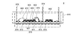
- the conventional semiconductor module 8 includes an insulating substrate 811, a conductor layer 812 provided on one surface of the insulating substrate 811, and other conductors provided at positions separated from the conductor layer 812.
- a substrate 810 having conductor layers 813 and 814, a first electrode 821 on one surface (the lower surface in FIG. 12), and two second electrodes 822 and 823 on the other surface (the upper surface in FIG. 12).
- one second electrode 822 is electrically connected to the terminal 874 through the wire 870 and another conductor layer 813, and the other second electrode 823. Is electrically connected to a terminal 876 through a wire 872.
- the conventional semiconductor module 8 includes the resin portion 860 formed by arranging the resin in the bowl-shaped space formed by the substrate 810 and the wall portion 816, the semiconductor module 8 has a shock resistance.
- the inventors of the present invention have conceived a semiconductor module capable of easily forming a structure for resin sealing, and have already filed an application as PCT / JP2015 / 051655 (hereinafter referred to as a prior application). .
- the semiconductor module 9 includes a first substrate 910 having a first conductive layer 912 provided on at least one surface of the first insulating substrate 911 and the first insulating substrate 911.
- a device portion (semiconductor element) 920 having a first electrode 921 on one side and a second electrode 922 on the other side, the first electrode 921 being joined to the first conductor layer 912;
- a second insulating layer 932 provided on at least one surface of the second insulating substrate 931 and the second insulating substrate 931, and the second conductive layer 932 is joined to the second electrode 922, and a planar surface
- the surrounding wall 934 is formed at a position surrounding the bonding portion 933 with the upper end surface protruding from the bonding surface between the bonding portion 933 and the second electrode 922, and the first wall via the surrounding wall portion 934 is provided.
- the substrate 910 It includes a second substrate 930, is defined by the surrounding wall portion 934, and a
- the device portion 920 is disposed so that the entire device portion 920 is located inside the region defined by the surrounding wall portion 934 in plan view.
- the second conductor layer 932 is positioned so as to surround the bonding portion 933 in plan view, and the upper end surface is above the bonding surface between the bonding portion 933 and the second electrode 922. Since it has the surrounding wall part 934 formed in the protruding state, there is no need to separately prepare a member for forming a structure for resin sealing (for example, the wall part 816 in the conventional semiconductor module 8), A structure for resin sealing can be easily formed.
- the second electrode 922 of the device portion 920 is joined to the second conductor layer 932, and therefore the second conductor layer 932 is electrically connected to the external connection terminal.
- the semiconductor module 9 according to the prior application is a semiconductor module having higher reliability than the conventional one.
- the semiconductor module 9 according to the prior application is a semiconductor module having higher heat dissipation than before.
- the control IC has a fine structure. It is preferable to connect the output terminal of the control IC and the gate electrode via a connecting member (for example, a wire or the like) having a small length.
- the joint portion 933 of the second substrate 930 and the second electrode 922 of the device portion 920 are joined (that is, the second substrate 930 is disposed on the device portion 920). Furthermore, since the device portion 920 is disposed so that the entire device portion 920 is located inside the region defined by the surrounding wall portion 934 in plan view, the power device portion (power When a semiconductor device is used, there is a problem that the gate electrode of the power device portion and the output terminal of the control IC cannot be connected with a connection member (wire or the like) having a small diameter.
- An object of the present invention is to provide a semiconductor module capable of controlling a power device unit with a control IC by connecting the output terminal of the IC with a connecting member having a small diameter.
- a semiconductor module of the present invention includes a first substrate having a first insulating substrate and a first conductor layer provided on at least one surface of the first insulating substrate, and a first electrode on one surface. And having a second electrode and a gate electrode on the other surface, wherein the first electrode is joined to the first conductor layer, a second insulating substrate, and a second insulating substrate.
- a second conductor layer provided on at least one surface, wherein the second conductor layer is joined to the second electrode, and the upper end surface is located at a position surrounding the joined portion in plan view; And a second substrate that is in contact with the first substrate through the surrounding wall portion, and the surrounding wall portion includes a surrounding wall portion that is formed in a state protruding from the bonding surface between the first electrode and the second electrode. And is sandwiched between the first insulating substrate and the second insulating substrate.
- An inner resin portion made of resin disposed in a space, a control IC disposed at a position separated from the power device portion, and the second substrate and the control IC on one side of the first substrate.
- At least an outer resin portion made of a resin arranged so as to cover the power device portion, wherein the power device portion is positioned so that the gate electrode is located outside a region defined by the surrounding wall portion in a plan view. It is arranged, and the gate electrode is electrically connected to the output terminal of the control IC through a predetermined connecting member.
- the surrounding wall portion formed at a position surrounding the joint portion is not only the case where the surrounding wall portion is formed around the joint portion, The case where the surrounding wall portion is formed only in a part of the periphery of the joint portion is also included.
- “at least covering the second substrate and the control IC” means not only the case where only the second substrate and the control IC are covered, but also the gate of the power device section in addition to the second substrate and the control IC. This includes the case of covering the electrode, a part of the first insulating substrate, a part of each conductor layer, and / or a connection member.
- the surrounding wall portion is formed only in a predetermined portion of the position surrounding the joint portion in plan view.
- the power device portion includes one semiconductor element, and the semiconductor element has a first electrode on one surface and a second electrode and a gate electrode on the other surface. It is preferable to have.
- the power device unit has a structure in which a plurality of semiconductor elements are stacked, and at least two of the plurality of semiconductor elements are on one side.
- a first electrode, and a second electrode and a gate electrode on the other surface, and the at least two semiconductor elements are positioned so as not to overlap each other in plan view. It is preferable that semiconductor elements are stacked.
- the power device section has a structure in which a plurality of semiconductor elements are stacked, and at least one of the plurality of semiconductor elements has a first surface on one surface. It is preferable to have an electrode and have the second electrode and the gate electrode on the other surface.
- the surrounding wall portion is formed in a state of being continuous with the joint portion, and the first substrate is the first conductor layer on one surface of the first insulating substrate.
- a groove for engaging with the surrounding wall is formed in the third conductor layer.
- the surrounding wall portion is formed in a state of being separated from the joint portion.
- the first substrate is joined to the surrounding wall portion at a position spaced from the first conductor layer on one surface of the first insulating substrate.
- the third conductor layer further includes a groove portion for engaging with the surrounding wall portion.
- a power device portion mounting conductor layer is provided on the other surface of the second substrate, and the power device portion mounting conductor layer includes a second power. It is preferable that the device part is arranged.
- the second power device portion has a first electrode electrically connected to the power device portion mounting conductor layer on one surface, and the second insulation.
- the conductive substrate has a hole provided at a position corresponding to the joint, a second connecting member is disposed inside the hole of the second insulating substrate, and the first power device unit includes the first connecting member. It is preferable that the electrode is electrically connected to the second electrode of the power device unit via the second connection member.
- the joining portion and the surrounding wall portion are formed from one copper layer.
- the semiconductor module of the present invention since the power device portion is arranged so that the gate electrode is located outside the region defined by the surrounding wall portion in plan view, the second portion is mostly on the power device portion. Even when the substrate is provided, the gate electrode of the power device unit and the output terminal of the control IC can be connected by a joining member (wire or the like) having a small diameter. As a result, the semiconductor module of the present invention becomes a semiconductor module capable of controlling the power device unit with the control IC.
- the second conductor layer has the surrounding wall portion formed at a position surrounding the joint portion in a plan view, so that heat is generated when an excessive load is applied to the power device portion. Even if the inner resin portion ignites, the surrounding wall portion can serve as a fire barrier to prevent the surrounding fire from spreading.
- the second conductor layer has the surrounding wall portion formed at a position surrounding the joint portion in plan view, so that the power device portion is shielded from the outside by the surrounding wall portion. Therefore, it is possible to prevent the power device unit from oscillating due to noise from the outside of the power device unit.
- the semiconductor module of the present invention is a semiconductor module with less defects due to oscillation.
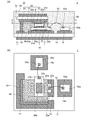
- FIG. 1 is a diagram illustrating a semiconductor module 1 according to a first embodiment.
- 1A is a cross-sectional view of the semiconductor module 1
- FIG. 1B is a plan cross-sectional view taken along line AA of FIG. 1A.
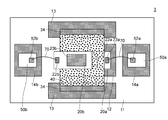
- FIG. 3 is a view for explaining a second substrate 30.
- 2A is a plan view of the second substrate 30, and
- FIG. 2B is a cross-sectional view taken along the line BB of FIG. 2A.
- FIG. 6 is a diagram illustrating a semiconductor module 2 according to a second embodiment.
- 3A is a cross-sectional view of the semiconductor module 2
- FIG. 3B is a CC cross-sectional view of FIG. 3A.
- 7 is a cross-sectional view showing a semiconductor module 2a according to Modification 1.
- FIG. 1A is a cross-sectional view of the semiconductor module 1
- FIG. 1B is a plan cross-sectional view taken along line AA of FIG. 1A.
- FIG. 6 is a plan sectional view showing a semiconductor module 3 according to a third embodiment.
- FIG. 6 is a diagram illustrating a semiconductor module 4 according to a fourth embodiment.
- 6A is a cross-sectional view of the semiconductor module 4
- FIG. 6B is a DD cross-sectional view of FIG. 6A.
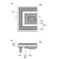
- FIG. 6 is a cross-sectional view showing a semiconductor module 5 according to a fifth embodiment. It is a figure shown in order to demonstrate the 2nd board
- FIG. 8A is a plan view of the second substrate 30a
- FIG. 8B is an EE cross-sectional view of FIG. 8A.
- FIG. 9 is a cross-sectional view showing a semiconductor module 6 according to a sixth embodiment.
- FIG. 10 is a cross-sectional view showing a semiconductor module 6a according to Modification 2.
- FIG. 10 is a plan sectional view showing a semiconductor module 7 according to Modification 3.
- FIG. It is sectional drawing which shows the conventional semiconductor module 8.
- Reference numeral 815 denotes a heat dissipating conductor layer of the substrate 810.
- Reference numeral 913 indicates a third conductor layer
- reference numeral 915 indicates a heat dissipation conductor layer of the first substrate 910
- reference numeral 916 indicates a groove
- reference numeral 935 indicates a heat dissipation conductor layer of the second substrate 930.
- Reference numeral 937 indicates a flat portion
- reference numeral S indicates solder.
- the semiconductor module 1 according to Embodiment 1 includes a first substrate 10, a power device unit, a second substrate 30, an inner resin unit 40, A control IC 50, an outer resin part 60, and a wire (connection member) 70 are provided.
- the first substrate 10 is a first insulating substrate 11, a first conductor layer 12 provided on one surface of the first insulating substrate 11, and a position that is separated from the first conductor layer 12.
- a third conductor layer 13 joined to the wall 34, a fourth conductor layer 14 provided with a control IC 50 at a position separated from the first conductor layer 12 and the third conductor layer 13,
- This is a mounting substrate having a heat dissipating conductor layer 15 provided on the other surface of the first insulating substrate 11.
- the first insulating substrate 11 is made of ceramics (for example, alumina), and the first conductor layer 12, the third conductor layer 13, the fourth conductor layer 14, and the heat dissipation conductor layer 15. Is made of metal (for example, copper).
- the first substrate 10 is a DCB substrate (Direct Copper Bonding substrate) in which the first insulating substrate 11 and each conductor layer are bonded by eutectic bonding. By setting it as such a structure, it becomes a semiconductor module which has high heat dissipation.
- the third conductor layer 13 is formed with a groove 16 for engaging with an enclosure wall 34 described later.
- the groove portion 16 is formed by etching the third conductor layer. Note that the third conductor layer 13 can be connected to the outside by being partially not covered with resin or being electrically connected to a terminal for external connection.
- the power device section is composed of one semiconductor element 20, has a first electrode 21 on one side (lower side in FIG. 1), and a second electrode 22 and a gate electrode 23 on the other side (upper side in FIG. 1). Have The power device portion is arranged such that the gate electrode 23 is located outside the region defined by the surrounding wall portion 34 in plan view.
- the semiconductor element 20 is a three-terminal semiconductor element (for example, IGBT).
- the gate electrode 23 is electrically connected to the output terminal 52 of the control IC 50 through a wire 70 described later.
- the first electrode 21 is joined to the first conductor layer 12, and the second electrode 22 is joined to a joint portion 33 of the second substrate 30 described later via a joining material S (for example, solder).
- the second substrate 30 includes a second insulating substrate 31, a second conductor layer 32 provided on one surface of the second insulating substrate 31, and the second insulating substrate 31. It has a heat radiating conductor layer 35 provided on the other surface, and the second conductor layer 32 is joined to the second electrode 22, and the upper end surface is joined to the joint portion 33 in plan view. 33 and the surrounding wall part 34 and the flat part 37 which were formed in the state which protruded from the joining surface of the 2nd electrode 22, and the 3rd conductor layer 13 of the 1st board
- the second insulating substrate 31 is made of ceramics (for example, alumina), and the second conductor layer 32 and the heat radiating conductor layer 35 are made of metal (for example, copper).
- the second substrate 30 is a DCB substrate in which the second insulating substrate 31 and each conductor layer are bonded by eutectic bonding.
- the joint portion 33 and the surrounding wall portion 34 are formed by etching one copper layer. By setting it as such a structure, the junction part 33 and the surrounding wall part 34 can be formed accurately.
- the surrounding wall portion 34 is formed only at a position that surrounds 3 ⁇ 4 of the entire circumference of the joint portion 33 in a position surrounding the joint portion 33 in plan view (see FIG. 1B). That is, the shape of the surrounding wall portion 34 is a “U” shape in plan view.
- the surrounding wall portion 34 is formed in a state of being continuous with the joint portion 33 through the flat portion 37 of the second conductor layer 32.
- the surrounding wall portion 34 is engaged with the groove portion 16 of the third conductor layer 13 of the first substrate 10 and is bonded via a bonding material (for example, solder). Accordingly, the third conductor layer 13 is electrically connected to the second electrode 22 through the surrounding wall portion 34 and the joint portion 33.
- the length from the boundary surface between the second insulating substrate 31 and the second conductor layer 32 to the upper end surface of the surrounding wall portion 34 is, for example, in the range of 0.2 to 1.0 mm.
- the thickness of the joint portion 33 is, for example, in the range of 0.15 to 0.5 mm.
- the inner resin portion 40 is made of resin disposed in “a space defined by the surrounding wall portion 34 and sandwiched between the first insulating substrate 11 and the second insulating substrate 31”.
- An appropriate resin for example, epoxy resin
- the inner resin portion 40 is located through a space sandwiched between the first insulating substrate 11 and the second insulating substrate 31 at a position where the surrounding wall portion 34 is not formed in a position surrounding the joint portion 33 in plan view. The resin is injected.
- the control IC 50 controls driving of the power device unit by controlling on / off of the gate electrode 23 of the power device unit.
- the control IC 50 is arranged via a fourth conductor layer 14 and a bonding material (for example, solder) at a position separated from the power device unit.
- the control IC 50 has a predetermined output terminal 52, and the output terminal 52 and the gate electrode 23 are electrically connected via a wire 70.
- the outer resin part 60 is made of resin arranged on one surface side of the first substrate 10 so as to cover the gate electrode 23 of the power device part, the second substrate 30 and the control IC 50.
- the resin constituting the outer resin part 60 the same resin as that of the inner resin part 40 is used, but a different resin can also be used.
- connection member 70 an appropriate wire can be used as long as the wire has a small diameter.
- a gold wire can be used as the wire (connection member) 70.
- the power device portion is arranged so that the gate electrode 23 is located outside the region defined by the surrounding wall portion 34 in plan view. Therefore, even when the second substrate 30 is provided on most of the power device section, the gate electrode 23 of the power device section and the output terminal 52 of the control IC 50 are connected by the wire 70 having a small diameter. Can do.
- the semiconductor module 1 according to the first embodiment is a semiconductor module in which the power device unit can be controlled by the control IC 50.
- the second conductor layer 32 has the surrounding wall portion 34 formed at a position surrounding the joint portion 33 in a plan view, so that an excessive load is applied to the power device portion. Even when the inner resin portion 40 is ignited by the heat generated when the fire is applied, it is possible to prevent the surrounding fire from spreading by the surrounding wall portion 34 serving as a fire barrier.
- the semiconductor module 1 according to the first embodiment since the second conductor layer 32 includes the surrounding wall portion 34 having the above-described configuration, the power device portion can be shielded from the outside by the surrounding wall portion 34. Therefore, it is possible to prevent the power device unit from oscillating due to noise from the outside of the power device unit. As a result, the semiconductor module 1 according to the first embodiment is a semiconductor module with few problems due to oscillation.
- the surrounding wall portion 34 is formed only in a predetermined portion of the position surrounding the joint portion 33 in plan view, and thus forms the inner resin portion 40.
- a space sandwiched between the first insulating substrate 11 and the second insulating substrate 31 at a position where the surrounding wall portion 34 is not formed in a position surrounding the joint portion 33 in plan view Resin can be injected.
- the power device unit includes the single semiconductor element 20, the semiconductor element 20 has the first electrode 21 on one surface, and the second surface has the first electrode 21. Since it has the two electrodes 22 and the gate electrode 23, it becomes a semiconductor module with a simple wiring design.
- the surrounding wall portion 34 is formed in a state of being continuous with the joint portion 33, and the first substrate 10 is connected to the first conductor layer 12 on one surface of the second insulating substrate 31.
- the third conductor layer 13 is further joined to the surrounding wall portion 34 at a spaced position, and the third conductor layer 13 is electrically connected to the second electrode 22 via the joining portion 33 and the surrounding wall portion 34. It is connected.
- the second electrode 22 of the power device portion can be electrically connected to the outside via the joint portion 33, the surrounding wall portion 34, and the third conductor layer 13.
- junction part 33, the surrounding wall part 34, and the 3rd conductor layer 13 have a cross-sectional area larger than a wire and resistance is low, it is hard to produce a malfunction when a big electric current is sent through a semiconductor module, and much higher reliability. It becomes a semiconductor module having properties.
- the semiconductor module 1 since it has the above-described configuration, the heat generated in the power device portion is radiated to the outside via the joint portion 33, the surrounding wall portion 34, and the third conductor layer 13. Thus, a semiconductor module having even higher heat dissipation can be obtained.
- the third conductor layer 13 is formed with the groove 16 for engaging with the surrounding wall portion 34.
- the surrounding wall portion 34 of the second substrate 30 can be easily positioned by being fitted into the groove portion 16 of the third conductor layer.
- the joint portion 33 and the surrounding wall portion 34 are formed from one copper layer, a joint material (for example, solder) is used in the manufacturing process of the semiconductor module. Even when it is put in a high-temperature furnace to melt it, the length of the surrounding wall 34 hardly changes. Accordingly, since the load of the second substrate 30 is distributed to the surrounding wall portion 34, the load of the second substrate 30 does not concentrate on the power device portion. As a result, the power device part is less likely to be broken in the manufacturing process of the semiconductor module, so that not only the semiconductor module with a high yield is obtained, but also when it is put in a high temperature furnace to melt the bonding material (for example, solder). The thickness of the bonding material can be prevented from changing, and a highly reliable semiconductor module can be obtained.
- a joint material for example, solder
- the joint portion 33 and the surrounding wall portion 34 are formed from one copper layer, the surrounding wall portion 34 is not inclined, In the manufacturing process of the semiconductor module, the second substrate 30 can be accurately positioned without the second substrate 30 rotating in the ⁇ direction in plan view.
- the semiconductor module 2 according to the second embodiment basically has the same configuration as the semiconductor module 1 according to the first embodiment, but the configuration of the power device unit is different from that of the semiconductor module 1 according to the first embodiment. That is, in the semiconductor module 2 according to the second embodiment, the power device unit has a structure in which two semiconductor elements 20a and 20b are stacked as shown in FIG.
- Both of the two semiconductor elements 20a and 20b have the first electrodes 21a and 21b on one side, and the second electrodes 22a and 22b and the gate electrodes 23a and 23b on the other side.
- the two semiconductor elements 20a and 20b are stacked so that the gate electrodes 23a and 23b of the two semiconductor elements 20a and 20b are positioned so as not to overlap each other in plan view. That is, the two semiconductor elements 20a and 20b are stacked while being shifted from each other by an angle of 90 °.
- the gate electrodes 23a and 23b are connected to output terminals 52a and 52b of separate control ICs 50a and 50b, respectively.
- the surrounding wall portion 34 is formed only at a position surrounding the entire circumference of the joint portion 33 in a position surrounding the joint portion 33 in a plan view (see FIG. 3B). That is, the shape of the surrounding wall portion 34a is an “L” shape in plan view.
- the semiconductor module 2 according to the second embodiment is different from the semiconductor module 1 according to the first embodiment in the configuration of the power device unit. Since the power device portion is arranged so that the gate electrodes 23a and 23b are located outside the region defined by the surrounding wall portion 34 in the view, the second substrate 30 is provided on the majority of the power device portion. Even if it exists, the gate electrodes 23a and 23b of a power device part and the output terminals 52a and 52b of control IC50a, 50b can be connected with the wire 70 with a small diameter. As a result, the semiconductor module 2 according to the second embodiment is a semiconductor module in which the power device unit can be controlled by the control ICs 50a and 50b.
- the power device unit has a structure in which the two semiconductor elements 20a and 20b are stacked. Therefore, the two semiconductor elements 20a and 20b are connected to the first insulating substrate 11. Occupied area can be made narrower than the case where they are arranged side by side. As a result, the semiconductor module satisfies the demand for product miniaturization.
- the two semiconductor elements 20a and 20b are stacked so that the gate electrodes 23a and 23b of the two semiconductor elements 20a and 20b are positioned so as not to overlap each other in plan view. Therefore, the gate electrodes 23a, 23b and the output terminals 52a, 52b of the control ICs 50a, 50b can be connected via the wires 70 without being obstructed by the semiconductor elements or the surrounding wall 34.
- the semiconductor elements 20a and 20b can be controlled by the control ICs 50a and 50b. As a result, it becomes a semiconductor module capable of controlling each semiconductor element while satisfying the demand for product miniaturization.
- the semiconductor module 2 according to the second embodiment has the same configuration as that of the semiconductor module 1 according to the first embodiment except for the configuration of the power device unit. Of which, it has a corresponding effect.
- the semiconductor module 2a according to the modification 1 basically has the same configuration as that of the semiconductor module 2 according to the second embodiment, but the configuration of the power device unit is different from that of the semiconductor module 1 according to the first embodiment. That is, in the semiconductor module 2a according to the first modification, the power device unit has a structure in which the two-terminal semiconductor element 20c is stacked on the three-terminal semiconductor element 20a as shown in FIG.
- the two-terminal semiconductor element 20c has a first electrode 21c formed on one side (lower side) electrically connected to the second electrode 22a of the three-terminal semiconductor element 20a.
- the second electrode 22c formed on the other surface (upper side surface) is electrically connected to the joint portion 33.
- the semiconductor module 2a according to the modification 1 is different from the semiconductor module 2 according to the second embodiment in the configuration of the power device unit, but is similar to the semiconductor module 2 according to the second embodiment. Since the power device portion is arranged so that the gate electrode 23a is located outside the region defined by the surrounding wall portion 34 when viewed, the second substrate 30 is provided on a large portion of the power device portion. In addition, the gate electrode 23a of the power device section and the output terminal 52 of the control IC 50 can be connected by a wire 70 having a small diameter. As a result, the semiconductor module 2a according to the first modification is a semiconductor module that can control the power device unit with the control IC 50.
- the semiconductor module 3 according to the third embodiment basically has the same configuration as the semiconductor module 2 according to the second embodiment, but the configuration of the power device unit is different from that of the semiconductor module 2 according to the second embodiment. That is, in the semiconductor module 3 according to the third embodiment, the power device unit has a structure in which the two semiconductor elements 20a and 20b are stacked in a state of being shifted by 180 ° as shown in FIG.
- the surrounding wall portion 34 is formed only at a predetermined position (a position where two straight straight lines are parallel to each other) among positions surrounding the joint portion 33 in plan view.
- the configuration of the power device unit is different from that in the semiconductor module 2 according to the second embodiment, but as in the case of the semiconductor module 2 according to the second embodiment, Since the power device portion is arranged so that the gate electrodes 23a and 23b are located outside the region defined by the surrounding wall portion 34 in the view, the second substrate 30 is provided on the majority of the power device portion. Even if it exists, the gate electrodes 23a and 23b of a power device part and the output terminals 52a and 52b of control IC50a, 50b can be connected with the wire 70 with a small diameter. As a result, the semiconductor module 3 according to the third embodiment is a semiconductor module in which the power device unit can be controlled by the control ICs 50a and 50b.
- the power device unit has a structure in which the two semiconductor elements 20a and 20b are stacked in a state of being shifted by 180 °, and thus the gate electrode 23a and the gate electrode 23b The interval can be increased, and the possibility of discharge between the gate electrodes can be reliably prevented.
- the power device unit has a structure in which the two semiconductor elements 20a and 20b are stacked in a state of being shifted by 180 °. can do.
- the semiconductor module 3 according to the third embodiment has the same configuration as that of the semiconductor module 2 according to the second embodiment except for the configuration of the power device unit, the effects of the semiconductor module 2 according to the second embodiment are obtained. Of which, it has a corresponding effect.
- the semiconductor module 4 according to the fourth embodiment basically has the same configuration as that of the semiconductor module 2a according to the first modification, but the second electrode of the semiconductor element on the first substrate side and the semiconductor element on the second substrate side. This is different from the semiconductor module 2a according to Modification 1 in that the first electrode is connected to the first electrode via a connection member. That is, in the semiconductor module 4 according to the fourth embodiment, as shown in FIG. 6, the second electrode 22a of the semiconductor element 20a on the first substrate side and the first electrode 21c of the semiconductor element 20c on the second substrate side are connected. They are connected via a child (connection member) 80.
- the connector 80 is formed by bending a metal plate and has a larger cross-sectional area and lower resistance than a wire.
- the connector 80 is a fifth conductor layer provided on one surface of the first insulating substrate 11 at a position separated from the first conductor layer 12, the third conductor layer 13, and the fourth conductor layer 14. 17 is connected.
- the semiconductor module 4 according to the fourth embodiment is such that the second electrode of the semiconductor element on the first substrate side and the first electrode of the semiconductor element on the second substrate side are connected via the connection member.
- the gate electrode 23 is located outside the region defined by the surrounding wall portion 34 in plan view, as in the case of the semiconductor module 2a according to the first modification. Since the power device portion is arranged as described above, the gate electrode 23 of the power device portion and the output terminal 52 of the control IC 50 are connected to each other even if the second substrate 30 is provided on a large portion of the power device portion. It can be connected with a small wire 70.
- the semiconductor module 4 according to the fourth embodiment is a semiconductor module capable of controlling the power device unit with the control IC 50.
- the connector 80 has a cross-sectional area larger than that of the wire and has a low resistance. Therefore, the semiconductor module 4 is less prone to malfunction when a large current is passed through the semiconductor module.
- the semiconductor module 4 according to the fourth embodiment has points other than the point that the second electrode of the semiconductor element on the first substrate side and the first electrode of the semiconductor element on the second substrate side are connected via the connection member. Has the same configuration as that of the semiconductor module 2a according to the first modification, and therefore has a corresponding effect among the effects of the semiconductor module 2a according to the first modification.
- the semiconductor module 5 according to the fifth embodiment basically has the same configuration as the semiconductor module 1 according to the first embodiment, but the configuration of the second conductor layer is the same as that of the semiconductor module 1 according to the first embodiment. Different. That is, in the second conductor layer 32a in the semiconductor module 5 according to the fifth embodiment, as shown in FIGS. 7 and 8, the surrounding wall portion 34a is formed in a state of being separated from the joint portion 33a.
- the first substrate 10 further includes a third conductor layer 13 joined to the surrounding wall portion 34a at a position separated from the first conductor layer 12 on one surface of the first insulating substrate 11, and the third conductor
- the layer 13 is formed with a groove 16 for engaging with the surrounding wall 34a.
- the semiconductor module 5 according to the fifth embodiment is different from the semiconductor module 1 according to the first embodiment in the configuration of the second conductor layer, but is similar to the semiconductor module 1 according to the first embodiment. Since the power device portion is arranged so that the gate electrode 23 is located outside the region defined by the surrounding wall portion 34 in plan view, the second substrate 30 is provided on a large portion of the power device portion. Even if it exists, the gate electrode 23 of a power device part and the output terminal 52 of control IC50 can be connected with the wire 70 with a small diameter. As a result, the semiconductor module 5 according to the fifth embodiment is a semiconductor module capable of controlling the power device unit with the control IC 50.
- the surrounding wall portion 34a is formed in a state of being separated from the joint portion 33a, and therefore, with other conductor layers and semiconductor elements via the surrounding wall portion 34a. It is possible to prevent a short circuit and a semiconductor module that is difficult to be destroyed.
- the semiconductor module 5 according to the fifth embodiment has the same configuration as the semiconductor module 1 according to the first embodiment except for the configuration of the second conductor layer, the semiconductor module 1 according to the first embodiment has the same configuration. It has a corresponding effect among the effects.
- the semiconductor module 6 according to the sixth embodiment basically has the same configuration as that of the semiconductor module 1 according to the first embodiment, but is implemented in that the power device unit is also arranged on the other surface side of the second substrate. This is different from the case of the semiconductor module 1 according to the first embodiment. That is, in the semiconductor module 6 according to the sixth embodiment, as shown in FIG. 9, the power device portion mounting conductor layer 35a is provided on the other surface side of the second substrate 30, and the power device portion mounting is performed. The second power device portion is disposed on the conductive layer 35a.
- the second power device section is composed of one semiconductor element 20d, has a first electrode 21d on one surface, and has a second electrode 22d and a gate electrode 23d on the other surface.
- the first electrode 21d is connected to a conductor layer (not shown) provided on one surface of the first substrate 10 by a connecting member (not shown), and the second electrode 22d is for mounting the power device portion.
- the gate electrode 23d is electrically connected to a control IC 50d (separate from the control IC 50) via a wire 70.
- the gate electrode 23d is electrically connected to the conductor layer 35a.
- the power device portion mounting conductor layer 35 a is insulated by the second conductor layer 32 and the second insulating substrate 31.
- the semiconductor module 6 according to the sixth embodiment is different from the semiconductor module 1 according to the first embodiment in that the power device is also arranged on the other surface side of the second substrate.
- the power device portion is arranged so that the gate electrode 23 is located outside the region defined by the surrounding wall portion 34 in plan view. Even when the second substrate 30 is provided in the portion, the gate electrode 23 of the power device unit and the output terminal 52 of the control IC 50 can be connected by the wire 70 having a small diameter.
- the semiconductor module 4 according to the fourth embodiment is a semiconductor module capable of controlling the power device unit with the control IC 50.
- the power device portion mounting conductor layer 35 a is provided on the other surface side of the second substrate 30, and the power device portion mounting conductor layer 35 a Since the second power device portion (semiconductor element 20d) is arranged, the occupation area may be made narrower than the case where the two semiconductor elements 20a and 20d are arranged side by side on one surface of the first insulating substrate 11. it can. As a result, the semiconductor module satisfies the demand for product miniaturization.
- the semiconductor module 6 according to the sixth embodiment has the same configuration as the semiconductor module 1 according to the first embodiment except that the power device unit is also arranged on the other surface side of the second substrate.
- the semiconductor module 1 according to the first embodiment has a corresponding effect among the effects of the semiconductor module 1.
- the semiconductor module 6a according to the modification 2 has basically the same configuration as the semiconductor module 6 according to the sixth embodiment, but the power device unit mounting conductor layer 35a is electrically connected to the second conductor layer 32. It is different from the semiconductor module 6 according to the sixth embodiment in that it is connected. That is, in the semiconductor module 6a according to the modified example 2, the second insulating substrate 31 is provided with a hole at a position corresponding to the joint portion 33 as shown in FIG. A connection member 82 is disposed on the inner side, and the power device portion mounting conductor layer 35 a is electrically connected to the second conductor layer 32 via the connection member 82.
- the connecting member 82 is obtained by punching and bending a metal plate.
- the semiconductor module 6a according to the modification 2 is the case of the semiconductor module 6 according to the sixth embodiment in that the power device portion mounting conductor layer 35a is electrically connected to the second conductor layer 32.
- the power device unit is arranged so that the gate electrode 23a is located outside the region defined by the surrounding wall unit 34 in plan view. Therefore, even when the second substrate 30 is provided on most of the power device portion, the gate electrode 23a of the power device portion and the output terminal 52 of the control IC 50 can be connected by the wire 70 having a small diameter.
- the semiconductor module 6a according to the modification 2 is a semiconductor module in which the power device unit can be controlled by the control IC 50.
- the power device unit has a structure in which two semiconductor elements are stacked, but the present invention is not limited to this.
- the power device unit may have a structure in which three or more semiconductor elements are stacked (see the semiconductor module 7 according to the third modification, FIG. 11).
- the two semiconductor elements are stacked in a state shifted by 90 °
- the two semiconductor elements are stacked in a state shifted by 180 °. It is not limited to.
- two or more semiconductor elements may be stacked in a state of being shifted by 45 ° (for example, the semiconductor module 7 according to Modification 3; see FIG. 11), or may be stacked in a state of being shifted at other angles. Also good.
- the first substrate is a DCB substrate, but the present invention is not limited to this.
- the first substrate may be a general printed board or an aluminum board.
- the second substrate is a DCB substrate, but the present invention is not limited to this.
- the second substrate may be a general printed board or an aluminum board.
- the heat dissipating conductor layer is provided on the other side of the first substrate and the other side of the second substrate.
- a conductor layer for mounting electronic components may be provided on at least one of the other surface side of the first substrate and the other surface side of the second substrate, or the conductor layer itself may not be provided.
- heat radiation fins may be disposed on the heat radiation conductor layer 15 (or on the heat radiation conductor layer 35).
- the joint portion and the surrounding wall portion are formed by etching one conductor layer, but the present invention is not limited to this.
- the joining portion and the surrounding wall portion may be formed separately, and the joining portion and the surrounding wall portion may be formed by joining them to the second substrate.
- the third conductor layer is formed with a groove for engaging with the surrounding wall, but the present invention is not limited to this.
- the groove portion may not be formed in the third conductor layer.
- the second power device unit includes one semiconductor element 20d, but the present invention is not limited to this.
- the second power device unit may have a structure in which a plurality of semiconductor elements are stacked.
Landscapes
- Cooling Or The Like Of Semiconductors Or Solid State Devices (AREA)
- Chemical & Material Sciences (AREA)
- Engineering & Computer Science (AREA)
- Structures Or Materials For Encapsulating Or Coating Semiconductor Devices Or Solid State Devices (AREA)
- Ceramic Engineering (AREA)
- Dispersion Chemistry (AREA)
- Microelectronics & Electronic Packaging (AREA)
- Wire Bonding (AREA)
- Inverter Devices (AREA)
Abstract
本発明の半導体モジュール1は、第1絶縁性基板11及び第1導電体層12を有する第1基板10と、第1電極21、第2電極22及びゲート電極23を有するパワーデバイス部と、第2絶縁性基板31及び第2導電体層32を有し、第2導電体層32が、接合部33及び平面視において接合部33を取り囲む位置に形成された囲繞壁部34を有する第2基板30と、内側樹脂部40と、制御IC50と、外側樹脂部60とを備え、平面視において囲繞壁部34によって画定された領域の外側にゲート電極23が位置するようにパワーデバイス部が配置され、ゲート電極23が、接続部材70を介して制御IC50の出力端子52と電気的に接続されている。 本発明のパワー半導体装置によれば、パワーデバイス部上の大部分に第2基板が配置されている場合であっても制御ICでパワーデバイス部を制御可能な半導体モジュールを提供することができる。
Description
本発明は、半導体モジュールに関する。
従来、基板と半導体素子とを備える半導体モジュールが知られている(例えば、特許文献1参照。)。
従来の半導体モジュール8は、図12に示すように、絶縁性基板811、絶縁性基板811の一方面に設けられた導電体層812及び導電体層812とは離間した位置に設けられた他の導電体層813,814を有する基板810と、一方面(図12の下側の面)に第1電極821を有し他方面(図12の上側の面)に2つの第2電極822,823を有し、第1電極821が導電体層812に接合されたデバイス部(半導体素子)820と、絶縁性基板811の外周に沿って形成された壁部816と、絶縁性基板811と壁部816とで構成される升状の空間に樹脂を配置することにより形成された樹脂部860と、樹脂部860の上面に配置された樹脂製の蓋部862と、一方端が他の導電体層813,814と電気的に接続され、かつ、当該一方端から樹脂部860及び蓋部862を介して外部(鉛直上方)に向かって延出された外部接続用の端子874,876とを備える。
半導体素子820の2つの第2電極822,823のうち、一方の第2電極822は、ワイヤ870及び他の導電体層813を介して端子874と電気的に接続され、他方の第2電極823は、ワイヤ872を介して端子876と電気的に接続されている。
従来の半導体モジュール8は、基板810と壁部816とで構成される升状の空間に樹脂を配置することにより形成された樹脂部860を備えるため、耐衝撃性を有する半導体モジュールとなる。
ところで、近年、半導体モジュールの技術の分野においては、樹脂封止するための構造を容易に形成することができる半導体モジュールが求められている。
そこで、本発明の発明者らは、樹脂封止するための構造を容易に形成することができる半導体モジュールを想到し、PCT/JP2015/051655(以下、先願という。)として既に出願している。
先願に係る半導体モジュール9は、図13に示すように、第1絶縁性基板911及び第1絶縁性基板911の少なくとも一方面に設けられた第1導電体層912を有する第1基板910と、一方面に第1電極921を有し、かつ、他方面に第2電極922を有し、第1電極921が第1導電体層912に接合されたデバイス部(半導体素子)920と、第2絶縁性基板931及び第2絶縁性基板931の少なくとも一方面に設けられた第2導電体層932を有し、第2導電体層932が、第2電極922と接合する接合部933及び平面視において接合部933を取り囲む位置に上端面が接合部933と第2電極922との接合面よりも突出した状態で形成された囲繞壁部934を有し、囲繞壁部934を介して第1基板910と接している第2基板930と、囲繞壁部934によって画定され、かつ、第1絶縁性基板911及び第2絶縁性基板931に挟まれた空間に配置された樹脂からなる樹脂部940とを備える。
先願に係る半導体モジュール9においては、平面視において囲繞壁部934によって画定された領域の内側にデバイス部920全体が位置するようにデバイス部920が配置されている。
先願に係る半導体モジュール9によれば、第2導電体層932が平面視において接合部933を取り囲む位置に、かつ、上端面が接合部933と第2電極922との接合面よりも上に突出した状態で形成されている囲繞壁部934を有するため、樹脂封止するための構造を形成するための部材(例えば、従来の半導体モジュール8における壁部816)を別途準備する必要がなく、樹脂封止するための構造を容易に形成することができる。
また、先願に係る半導体モジュール9によれば、デバイス部920の第2電極922が第2導電体層932に接合されているため、第2導電体層932を外部接続用の端子と電気的に接続することにより、ワイヤよりも断面積が大きく抵抗が低い第2導電体層932を介してデバイス部920の第2電極922と外部接続用の端子とを電気的に接続することができる。従って、半導体モジュールに大電流を流したときに不具合が生じ難く、先願に係る半導体モジュール9は、従来よりも高い信頼性を有する半導体モジュールとなる。
また、先願に係る半導体モジュール9によれば、デバイス部920の第2電極922が、第2絶縁性基板931の一方面に設けられた第2導電体層932に接合されているため、デバイス部920で発生した熱を第1導電体層912及び第1絶縁性基板911を介して外部へ放熱するのに加えて、第2導電体層932及び第2絶縁性基板931を介して外部へ放熱することができる。従って、先願に係る半導体モジュール9は、従来よりも高い放熱性を有する半導体モジュールとなる。
ところで、このような半導体モジュールにおいて、デバイス部としてゲート電極を有するパワーデバイス部(パワー半導体素子)を用い、当該パワーデバイス部を制御ICで制御する場合、制御ICは微細な構造を有するため、径が小さい接続部材(例えばワイヤ等)を介して制御ICの出力端子とゲート電極とを接続することが好ましい。
しかしながら、先願に係る半導体モジュール9においては、第2基板930の接合部933とデバイス部920の第2電極922とが接合され(すなわち、デバイス部920の上に第2基板930が配置され)、さらには、平面視において囲繞壁部934によって画定された領域の内側にデバイス部920全体が位置するようにデバイス部920が配置されているため、デバイス部としてゲート電極を有するパワーデバイス部(パワー半導体素子)を用いた場合には、パワーデバイス部のゲート電極と制御ICの出力端子とを径が小さい接続部材(ワイヤ等)で接続することができない、という問題がある。
そこで、本発明は、上記した問題を解決するためになされたものであり、パワーデバイス部上の大部分に第2基板が配置されている場合であっても、パワーデバイス部のゲート電極と制御ICの出力端子とを径が小さい接続部材で接続することにより制御ICでパワーデバイス部を制御可能な半導体モジュールを提供することを目的とする。
[1]本発明の半導体モジュールは、第1絶縁性基板及び前記第1絶縁性基板の少なくとも一方面に設けられた第1導電体層を有する第1基板と、一方面に第1電極を有し、かつ、他方面に第2電極及びゲート電極を有し、前記第1電極が前記第1導電体層に接合されたパワーデバイス部と、第2絶縁性基板及び前記第2絶縁性基板の少なくとも一方面に設けられた第2導電体層を有し、前記第2導電体層が、前記第2電極と接合する接合部及び平面視において前記接合部を取り囲む位置に上端面が前記接合部と前記第2電極との接合面よりも突出した状態で形成された囲繞壁部を有し、前記囲繞壁部を介して前記第1基板と接している第2基板と、前記囲繞壁部によって画定され、かつ、前記第1絶縁性基板及び前記第2絶縁性基板に挟まれた空間に配置された樹脂からなる内側樹脂部と、前記パワーデバイス部とは離間した位置に配置された制御ICと、前記第1基板の一方面側に、前記第2基板及び前記制御ICを少なくとも覆うように配置された樹脂からなる外側樹脂部とを備える半導体モジュールであって、平面視において前記囲繞壁部によって画定された領域の外側に前記ゲート電極が位置するように前記パワーデバイス部が配置され、前記ゲート電極が、所定の接続部材を介して前記制御ICの出力端子と電気的に接続されていることを特徴とする。
なお、本明細書中、「接合部を取り囲む位置に・・・形成された囲繞壁部」とは、接合部の周囲のうちの全周に囲繞壁部が形成されている場合のみならず、接合部の周囲のうちの一部のみに囲繞壁部が形成されている場合も含む。また、本明細書中、「第2基板及び制御ICを少なくとも覆う」とは、第2基板及び制御ICのみを覆う場合だけでなく、第2基板及び制御ICの他に、パワーデバイス部のゲート電極、第1絶縁性基板の一部、各導電体層の一部及び(又は)接続部材等を覆う場合も含む。
[2]本発明の半導体モジュールにおいては、前記囲繞壁部は、平面視において前記接合部を取り囲む位置のうちの所定の部分のみに形成されていることが好ましい。
[3]本発明の半導体モジュールにおいては、前記パワーデバイス部は、1つの半導体素子からなり、前記半導体素子は、一方面に第1電極を有し、かつ、他方面に第2電極及びゲート電極を有することが好ましい。
[4]本発明の半導体モジュールにおいては、前記パワーデバイス部は、複数の半導体素子が積層された構造を有し、前記複数の半導体素子のうちの少なくとも2つの半導体素子はいずれも、一方面に第1電極を有し、かつ、他方面に第2電極及びゲート電極を有し、前記少なくとも2つの半導体素子のそれぞれの前記ゲート電極が平面視において重ならない位置に位置するように前記少なくとも2つの半導体素子が積層されていることが好ましい。
[5]本発明の半導体モジュールにおいては、前記パワーデバイス部は、複数の半導体素子が積層された構造を有し、前記複数の半導体素子のうちの少なくとも一つの半導体素子は、一方面に第1電極を有し、かつ、他方面に第2電極及びゲート電極を有することが好ましい。
[6]本発明の半導体モジュールにおいては、前記囲繞壁部は、前記接合部と連続した状態で形成され、前記第1基板は、前記第1絶縁性基板の一方面における前記第1導電体層と離間した位置で前記囲繞壁部と接合される第3導電体層をさらに有し、前記第3導電体層は、前記囲繞壁部及び前記接合部を介して前記第2電極と電気的に接続されていることが好ましい。
[7]本発明の半導体モジュールにおいては、前記第3導電体層には、前記囲繞壁部と係合するための溝部が形成されていることが好ましい。
[8]本発明の半導体モジュールにおいては、前記囲繞壁部は、前記接合部と離間した状態で形成されていることが好ましい。
[9]本発明の半導体モジュールにおいては、前記第1基板は、前記第1絶縁性基板の一方面における前記第1導電体層と離間した位置で前記囲繞壁部と接合される第3導電体層をさらに有し、前記第3導電体層は、前記囲繞壁部と係合するための溝部が形成されていることが好ましい。
[10]本発明の半導体モジュールにおいては、前記第2基板の他方面には、パワーデバイス部搭載用導電体層が設けられており、前記パワーデバイス部搭載用導電体層には、第2パワーデバイス部が配置されていることが好ましい。
[11]本発明の半導体モジュールにおいては、前記第2パワーデバイス部は、一方面に前記パワーデバイス部搭載用導電体層と電気的に接続されている第1電極を有し、前記第2絶縁性基板が、前記接合部に対応する位置に設けられた孔を有し、前記第2絶縁性基板の孔の内側には第2接続部材が配置され、前記第2パワーデバイス部の前記第1電極は、当該第2接続部材を介して前記パワーデバイス部の前記第2電極と電気的に接続されていることが好ましい。
[12]本発明の半導体モジュールにおいては、前記接合部及び前記囲繞壁部は、1の銅層から形成されたものであることが好ましい。
本発明の半導体モジュールによれば、平面視において囲繞壁部によって画定された領域の外側にゲート電極が位置するようにパワーデバイス部が配置されているため、パワーデバイス部上の大部分に第2基板を備える場合であっても、パワーデバイス部のゲート電極と制御ICの出力端子とを径の小さい接合部材(ワイヤ等)で接続することができる。その結果、本発明の半導体モジュールは、制御ICでパワーデバイス部を制御可能な半導体モジュールとなる。
また、本発明の半導体モジュールによれば、第2導電体層が、平面視において接合部を取り囲む位置に形成された囲繞壁部を有するため、パワーデバイス部に過大な負荷をかけたときの発熱によって内側樹脂部が発火した場合であっても、囲繞壁部が防火壁の役割を果たすことにより周囲への延焼を防ぐことができる。
また、本発明の半導体モジュールによれば、第2導電体層が、平面視において接合部を取り囲む位置に形成された囲繞壁部を有するため、パワーデバイス部を外部から囲繞壁部で遮蔽することができ、パワーデバイス部の外部からのノイズによってパワーデバイス部に発振が起こることを防ぐことができ、その結果、本発明の半導体モジュールは、発振による不具合が少ない半導体モジュールとなる。
以下、本発明の半導体モジュールについて、図に示す実施形態に基づいて説明する。
[実施形態1]
1.実施形態1に係る半導体モジュール1の構成
実施形態1に係る半導体モジュール1は、図1に示すように、第1基板10と、パワーデバイス部と、第2基板30と、内側樹脂部40と、制御IC50と、外側樹脂部60と、ワイヤ(接続部材)70とを備える
1.実施形態1に係る半導体モジュール1の構成
実施形態1に係る半導体モジュール1は、図1に示すように、第1基板10と、パワーデバイス部と、第2基板30と、内側樹脂部40と、制御IC50と、外側樹脂部60と、ワイヤ(接続部材)70とを備える
第1基板10は、第1絶縁性基板11と、第1絶縁性基板11の一方面に設けられた第1導電体層12と、第1導電体層12と離間した位置で、後述する囲繞壁部34と接合される第3導電体層13と、第1導電体層12及び第3導電体層13とは離間した位置に設けられ制御IC50が配置される第4導電体層14と、第1絶縁性基板11の他方面に設けられた放熱用導電体層15とを有する実装基板である。
第1基板10において、第1絶縁性基板11は、セラミックス(例えば、アルミナ)からなり、第1導電体層12、第3導電体層13、第4導電体層14及び放熱用導電体層15は、金属(例えば銅)からなる。第1基板10は、第1絶縁性基板11と各導電体層が共晶接合によって接合されているDCB基板(Direct Cupper Bonding基板)である。このような構成とすることにより、高い放熱性を有する半導体モジュールとなる。
第3導電体層13には、後述する囲繞壁部34と係合するための溝部16が形成されている。溝部16は第3導電体層をエッチングすることにより形成されたものである。なお、第3導電体層13は、一部が樹脂に覆われていないことにより、又は外部接続用の端子と電気的に接続されていることにより、外部との接続が可能となっている。
パワーデバイス部は、1つの半導体素子20からなり、一方面(図1の下側)に第1電極21を有し、かつ、他方面(図1の上側)に第2電極22及びゲート電極23を有する。パワーデバイス部は、平面視において囲繞壁部34によって画定された領域の外側にゲート電極23が位置するように配置されている。半導体素子20は、3端子の半導体素子(例えば、IGBT)である。
ゲート電極23は、後述するワイヤ70を介して制御IC50の出力端子52と電気的に接続されている。第1電極21は第1導電体層12と、第2電極22は後述する第2基板30の接合部33と、それぞれ接合材S(例えば、はんだ)を介して接合されている。
第2基板30は、図1及び図2に示すように、第2絶縁性基板31、第2絶縁性基板31の一方面に設けられた第2導電体層32及び第2絶縁性基板31の他方面に設けられた放熱用導電体層35を有し、第2導電体層32が、第2電極22と接合する接合部33、平面視において接合部33を取り囲む位置に上端面が接合部33と第2電極22との接合面よりも突出した状態で形成された囲繞壁部34及び平坦部37を有し、囲繞壁部34を介して第1基板10の第3導電体層13と接している。
第2基板30において、第2絶縁性基板31は、セラミックス(例えば、アルミナ)からなり、第2導電体層32及び放熱用導電体層35は、金属(例えば銅)からなる。第2基板30は、第2絶縁性基板31と各導電体層が共晶接合によって接合されているDCB基板である。なお、接合部33及び囲繞壁部34は、1の銅層をエッチングすることによって形成されたものである。このような構成とすることにより、接合部33及び囲繞壁部34を精度よく形成することができる。
囲繞壁部34は、平面視において接合部33を取り囲む位置のうちの接合部33の全周の3/4にわたって取り囲む位置にのみ形成されている(図1(b)参照。)。すなわち、囲繞壁部34の形状は、平面視において「コ」の字形状をしている。
囲繞壁部34は、第2導電体層32の平坦部37を介して接合部33と連続した状態で形成されている。囲繞壁部34は、第1基板10の第3導電体層13の溝部16に係合されており、接合材(例えばはんだ)を介して接合されている。これにより、第3導電体層13は、囲繞壁部34及び接合部33を介して第2電極22と電気的に接続されている。第2電極22と
第2絶縁性基板31と第2導電体層32との境界面から囲繞壁部34の上端面までの長さは例えば、0.2~1.0mmの範囲内にある。接合部33の厚みは、例えば0.15~0.5mmの範囲内にある。
内側樹脂部40は、図1に示すように、「囲繞壁部34によって画定され、かつ、第1絶縁性基板11及び第2絶縁性基板31に挟まれた空間」に配置された樹脂からなる。内側樹脂部40を構成する樹脂は、適宜の樹脂(例えば、エポキシ樹脂)を用いることができる。内側樹脂部40は、平面視において接合部33を取り囲む位置のうちの囲繞壁部34が形成されていない位置において第1絶縁性基板11と第2絶縁性基板31とで挟まれた空間を介して樹脂が注入されてなる。
制御IC50は、パワーデバイス部のゲート電極23のオンオフを制御することによりパワーデバイス部の駆動を制御する。制御IC50は、パワーデバイス部とは離間した位置において第4導電体層14と接合材(例えばはんだ)を介して配置されている。制御IC50は、所定の出力端子52を有し、当該出力端子52とゲート電極23とがワイヤ70を介して電気的に接続されている。
外側樹脂部60は、第1基板10の一方面側に、パワーデバイス部のゲート電極23、第2基板30及び制御IC50覆うように配置された樹脂からなる。外側樹脂部60を構成する樹脂は、内側樹脂部40の樹脂と同じ樹脂を用いるが異なる樹脂を用いることもできる。
ワイヤ(接続部材)70としては、径が細いワイヤであれば適宜のワイヤを用いることができ、例えば金線ワイヤを用いることができる。
2.実施形態1に係る半導体モジュール1の効果
実施形態1に係る半導体モジュール1によれば、平面視において囲繞壁部34によって画定された領域の外側にゲート電極23が位置するようにパワーデバイス部が配置されているため、パワーデバイス部上の大部分に第2基板30を備える場合であっても、パワーデバイス部のゲート電極23と制御IC50の出力端子52とを径の小さいワイヤ70で接続することができる。その結果、実施形態1に係る半導体モジュール1は、制御IC50でパワーデバイス部を制御可能な半導体モジュールとなる。
実施形態1に係る半導体モジュール1によれば、平面視において囲繞壁部34によって画定された領域の外側にゲート電極23が位置するようにパワーデバイス部が配置されているため、パワーデバイス部上の大部分に第2基板30を備える場合であっても、パワーデバイス部のゲート電極23と制御IC50の出力端子52とを径の小さいワイヤ70で接続することができる。その結果、実施形態1に係る半導体モジュール1は、制御IC50でパワーデバイス部を制御可能な半導体モジュールとなる。
また、実施形態1に係る半導体モジュール1によれば、第2導電体層32が、平面視において接合部33を取り囲む位置に形成された囲繞壁部34を有するため、パワーデバイス部に過大な負荷をかけたときの発熱によって内側樹脂部40が発火した場合であっても、囲繞壁部34が防火壁の役割を果たすことにより周囲への延焼を防ぐことができる。
また、実施形態1に係る半導体モジュール1によれば、第2導電体層32が、上記した構成を有する囲繞壁部34を有するため、パワーデバイス部を外部から囲繞壁部34で遮蔽することができ、パワーデバイス部の外部からのノイズによってパワーデバイス部に発振が起こることを防ぐことができ、その結果、実施形態1に係る半導体モジュール1は、発振による不具合が少ない半導体モジュールとなる。
また、実施形態1に係る半導体モジュール1によれば、囲繞壁部34は、平面視において接合部33を取り囲む位置のうちの所定の部分のみに形成されているため、内側樹脂部40を形成する際に、「平面視において接合部33を取り囲む位置のうちの囲繞壁部34が形成されていない位置において第1絶縁性基板11と第2絶縁性基板31とで挟まれた空間」を介して樹脂を注入することができる。
また、実施形態1に係る半導体モジュール1によれば、パワーデバイス部は、1つの半導体素子20からなり、当該半導体素子20は、一方面に第1電極21を有し、かつ、他方面に第2電極22及びゲート電極23を有するため、配線設計が簡便な半導体モジュールとなる。
実施形態1に係る半導体モジュール1において、囲繞壁部34は、接合部33と連続した状態で形成され、第1基板10は、第2絶縁性基板31の一方面における第1導電体層12と離間した位置で囲繞壁部34と接合される第3導電体層13をさらに有し、第3導電体層13は、接合部33及び囲繞壁部34を介して第2電極22と電気的に接続されている。
このような構成とすることにより、パワーデバイス部の第2電極22が、接合部33、囲繞壁部34及び第3導電体層13を介して外部と電気的に接続することができる。そして、接合部33、囲繞壁部34及び第3導電体層13はいずれもワイヤよりも断面積が大きく抵抗が低いため半導体モジュールに大電流を流したときに不具合が生じ難く、より一層高い信頼性を有する半導体モジュールとなる。
このような構成とすることにより、パワーデバイス部の第2電極22が、接合部33、囲繞壁部34及び第3導電体層13を介して外部と電気的に接続することができる。そして、接合部33、囲繞壁部34及び第3導電体層13はいずれもワイヤよりも断面積が大きく抵抗が低いため半導体モジュールに大電流を流したときに不具合が生じ難く、より一層高い信頼性を有する半導体モジュールとなる。
また、実施形態1に係る半導体モジュール1によれば、上記した構成を有するため、パワーデバイス部で発生した熱を接合部33、囲繞壁部34及び第3導電体層13を介して外部へ放熱することができ、より一層高い放熱性を有する半導体モジュールとなる。
また、実施形態1に係る半導体モジュール1によれば、第3導電体層13には、囲繞壁部34と係合するための溝部16が形成されているため、半導体モジュールの製造過程において、第1基板10上に第2基板30を搭載する際に、第2基板30の囲繞壁部34を第3導電体層の溝部16へはめ込むことで容易に位置決めすることができる。
また、実施形態1に係る半導体モジュール1によれば、接合部33及び囲繞壁部34は、1の銅層から形成されたものであるため、半導体モジュールの製造過程において、接合材(例えばはんだ)を溶融するために高温炉に入れたときであっても、囲繞壁部34の長さはほとんど変化しない。従って、第2基板30の荷重が囲繞壁部34に分散されるため、第2基板30の荷重がパワーデバイス部に集中することがない。その結果、半導体モジュールの製造過程においてパワーデバイス部が壊れにくくなるため、歩留りが高い半導体モジュールとなるだけでなく、接合材(例えばはんだ)を溶融するために高温炉に入れたときであっても、接合材の厚みが変化してしまうことを防ぐことができ、信頼性が高い半導体モジュールとなる。
また、実施形態1に係る半導体モジュール1によれば、接合部33及び囲繞壁部34は、1の銅層から形成されたものであるため、囲繞壁部34が傾いたりすることもないため、半導体モジュールの製造過程において、第2基板30が平面視においてθ方向に回転してしまうこともなく、第2基板30を正確に位置決めすることができる。
[実施形態2]
実施形態2に係る半導体モジュール2は、基本的には実施形態1に係る半導体モジュール1と同様の構成を有するが、パワーデバイス部の構成が実施形態1に係る半導体モジュール1の場合とは異なる。すなわち、実施形態2に係る半導体モジュール2において、パワーデバイス部は、図3に示すように、2つの半導体素子20a、20bが積層された構造を有する。
実施形態2に係る半導体モジュール2は、基本的には実施形態1に係る半導体モジュール1と同様の構成を有するが、パワーデバイス部の構成が実施形態1に係る半導体モジュール1の場合とは異なる。すなわち、実施形態2に係る半導体モジュール2において、パワーデバイス部は、図3に示すように、2つの半導体素子20a、20bが積層された構造を有する。
2つの半導体素子20a、20bはいずれも、一方面に第1電極21a、21bを有し、かつ、他方面に第2電極22a、22b及びゲート電極23a、23bを有する。2つの半導体素子20a、20bのそれぞれのゲート電極23a、23bが平面視において重ならない位置に位置するように2つの半導体素子20a、20bが積層されている。すなわち、2つの半導体素子20a、20bは互いに90°の角度でずらされた状態で積層されている。
各ゲート電極23a、23bは、別々の制御IC50a、50bの出力端子52a、52bとそれぞれ接続されている。
囲繞壁部34は、平面視において接合部33を取り囲む位置のうちの接合部33の全周の1/2の範囲にわたって取り囲む位置にのみ形成されている(図3(b)参照。)。すなわち、囲繞壁部34aの形状は、平面視において「L」の字形状をしている。
このように、実施形態2に係る半導体モジュール2は、パワーデバイス部の構成が実施形態1に係る半導体モジュール1の場合とは異なるが、実施形態1に係る半導体モジュール1の場合と同様に、平面視において囲繞壁部34によって画定された領域の外側にゲート電極23a、23bが位置するようにパワーデバイス部が配置されているため、パワーデバイス部上の大部分に第2基板30を備える場合であっても、パワーデバイス部のゲート電極23a、23bと制御IC50a、50bの出力端子52a、52bとを径の小さいワイヤ70で接続することができる。その結果、実施形態2に係る半導体モジュール2は、制御IC50a、50bでパワーデバイス部を制御可能な半導体モジュールとなる。
また、実施形態2に係る半導体モジュール2によれば、パワーデバイス部は、2つの半導体素子20a、20bが積層された構造を有することから、2つの半導体素子20a、20bを第1絶縁性基板11の一方面に並べて配置した場合よりも占有面積を狭くすることができる。その結果、製品の小型化の要請を満たす半導体モジュールとなる。
また、実施形態2に係る半導体モジュール2によれば、2つの半導体素子20a、20bのそれぞれのゲート電極23a、23bが平面視において重ならない位置に位置するように2つの半導体素子20a、20bが積層されているため、各ゲート電極23a、23bと制御IC50a、50bの出力端子52a、52bとを、互いの半導体素子や囲繞壁部34に邪魔されることなくワイヤ70を介して接続することができ、制御IC50a、50bで各半導体素子20a、20bを制御することができる。その結果、製品の小型化の要請を満たしつつ、各半導体素子を制御可能な半導体モジュールとなる。
なお、実施形態2に係る半導体モジュール2は、パワーデバイス部の構成以外の点においては実施形態1に係る半導体モジュール1と同様の構成を有するため、実施形態1に係る半導体モジュール1が有する効果のうち該当する効果を有する。
[変形例1]
変形例1に係る半導体モジュール2aは、基本的には実施形態2に係る半導体モジュール2と同様の構成を有するが、パワーデバイス部の構成が実施形態1に係る半導体モジュール1の場合とは異なる。すなわち、変形例1に係る半導体モジュール2aにおいて、パワーデバイス部は、図4に示すように、3端子の半導体素子20a上に2端子の半導体素子20cが積層された構造を有する。
変形例1に係る半導体モジュール2aは、基本的には実施形態2に係る半導体モジュール2と同様の構成を有するが、パワーデバイス部の構成が実施形態1に係る半導体モジュール1の場合とは異なる。すなわち、変形例1に係る半導体モジュール2aにおいて、パワーデバイス部は、図4に示すように、3端子の半導体素子20a上に2端子の半導体素子20cが積層された構造を有する。
変形例1に係る半導体モジュール2aにおいて、2端子の半導体素子20cは、一方面(下側面)に形成された第1電極21cが3端子の半導体素子20aの第2電極22aと電気的に接続されており、他方面(上側面)に形成された第2電極22cが接合部33と電気的に接続されている。
このように、変形例1に係る半導体モジュール2aは、パワーデバイス部の構成が実施形態2に係る半導体モジュール2の場合とは異なるが、実施形態2に係る半導体モジュール2の場合と同様に、平面視において囲繞壁部34によって画定された領域の外側にゲート電極23aが位置するようにパワーデバイス部が配置されているため、パワーデバイス部上の大部分に第2基板30を備える場合であっても、パワーデバイス部のゲート電極23aと制御IC50の出力端子52とを径の小さいワイヤ70で接続することができる。その結果、変形例1に係る半導体モジュール2aは、制御IC50でパワーデバイス部を制御可能な半導体モジュールとなる。
[実施形態3]
実施形態3に係る半導体モジュール3は、基本的には実施形態2に係る半導体モジュール2と同様の構成を有するが、パワーデバイス部の構成が実施形態2に係る半導体モジュール2の場合とは異なる。すなわち、実施形態3に係る半導体モジュール3において、パワーデバイス部は、図5に示すように、2つの半導体素子20a、20bが180°ずれた状態で積層された構造を有する。
実施形態3に係る半導体モジュール3は、基本的には実施形態2に係る半導体モジュール2と同様の構成を有するが、パワーデバイス部の構成が実施形態2に係る半導体モジュール2の場合とは異なる。すなわち、実施形態3に係る半導体モジュール3において、パワーデバイス部は、図5に示すように、2つの半導体素子20a、20bが180°ずれた状態で積層された構造を有する。
囲繞壁部34は、平面視において接合部33を取り囲む位置のうちの所定の位置(直線状の2本の直線が互いに平行となる位置)にのみ形成されている。
このように、実施形態3に係る半導体モジュール3は、パワーデバイス部の構成が実施形態2に係る半導体モジュール2の場合とは異なるが、実施形態2に係る半導体モジュール2の場合と同様に、平面視において囲繞壁部34によって画定された領域の外側にゲート電極23a、23bが位置するようにパワーデバイス部が配置されているため、パワーデバイス部上の大部分に第2基板30を備える場合であっても、パワーデバイス部のゲート電極23a、23bと制御IC50a、50bの出力端子52a、52bとを径の小さいワイヤ70で接続することができる。その結果、実施形態3に係る半導体モジュール3は、制御IC50a、50bでパワーデバイス部を制御可能な半導体モジュールとなる。
また、実施形態3に係る半導体モジュール3によれば、パワーデバイス部は、2つの半導体素子20a、20bが180°ずれた状態で積層された構造を有するため、ゲート電極23aとゲート電極23bとの間隔を長くすることができ、当該ゲート電極同士の間で放電するおそれを確実に防ぐことができる。
また、実施形態3に係る半導体モジュール3によれば、パワーデバイス部は、2つの半導体素子20a、20bが180°ずれた状態で積層された構造を有するため、比較的細長い領域に半導体モジュールを設置することができる。
なお、実施形態3に係る半導体モジュール3は、パワーデバイス部の構成以外の点においては実施形態2に係る半導体モジュール2と同様の構成を有するため、実施形態2に係る半導体モジュール2が有する効果のうち該当する効果を有する。
[実施形態4]
実施形態4に係る半導体モジュール4は、基本的には変形例1に係る半導体モジュール2aと同様の構成を有するが、第1基板側の半導体素子の第2電極と第2基板側の半導体素子の第1電極とが接続部材を介して接続されている点で変形例1に係る半導体モジュール2aの場合とは異なる。すなわち、実施形態4に係る半導体モジュール4においては、図6に示すように、第1基板側の半導体素子20aの第2電極22aと第2基板側の半導体素子20cの第1電極21cとが接続子(接続部材)80を介して接続されている。
実施形態4に係る半導体モジュール4は、基本的には変形例1に係る半導体モジュール2aと同様の構成を有するが、第1基板側の半導体素子の第2電極と第2基板側の半導体素子の第1電極とが接続部材を介して接続されている点で変形例1に係る半導体モジュール2aの場合とは異なる。すなわち、実施形態4に係る半導体モジュール4においては、図6に示すように、第1基板側の半導体素子20aの第2電極22aと第2基板側の半導体素子20cの第1電極21cとが接続子(接続部材)80を介して接続されている。
接続子80は、金属板を折り曲げて形成されたものであり、ワイヤよりも断面積が大きく抵抗が低い。接続子80は、第1絶縁性基板11の一方面に、第1導電体層12、第3導電体層13及び第4導電体層14とは離間した位置に設けられた第5導電体層17と接続されている。
このように、実施形態4に係る半導体モジュール4は、第1基板側の半導体素子の第2電極と第2基板側の半導体素子の第1電極とが接続部材を介して接続されている点で変形例1に係る半導体モジュール2aの場合とは異なるが、変形例1に係る半導体モジュール2aの場合と同様に、平面視において囲繞壁部34によって画定された領域の外側にゲート電極23が位置するようにパワーデバイス部が配置されているため、パワーデバイス部上の大部分に第2基板30を備える場合であっても、パワーデバイス部のゲート電極23と制御IC50の出力端子52とを径の小さいワイヤ70で接続することができる。その結果、実施形態4に係る半導体モジュール4は、制御IC50でパワーデバイス部を制御可能な半導体モジュールとなる。
また、実施形態4に係る半導体モジュール4によれば、接続子80は、ワイヤよりも断面積が大きく抵抗が低いため半導体モジュールに大電流を流したときに不具合が生じ難く、より一層高い信頼性を有する半導体モジュールとなる。
なお、実施形態4に係る半導体モジュール4は、第1基板側の半導体素子の第2電極と第2基板側の半導体素子の第1電極とが接続部材を介して接続されている点以外の点においては変形例1に係る半導体モジュール2aと同様の構成を有するため、変形例1に係る半導体モジュール2aが有する効果のうち該当する効果を有する。
[実施形態5]
実施形態5に係る半導体モジュール5は、基本的には実施形態1に係る半導体モジュール1と同様の構成を有するが、第2導電体層の構成が実施形態1に係る半導体モジュール1の場合とは異なる。すなわち、実施形態5に係る半導体モジュール5における第2導電体層32aにおいては、図7及び図8に示すように、囲繞壁部34aが、接合部33aと離間した状態で形成されている。
実施形態5に係る半導体モジュール5は、基本的には実施形態1に係る半導体モジュール1と同様の構成を有するが、第2導電体層の構成が実施形態1に係る半導体モジュール1の場合とは異なる。すなわち、実施形態5に係る半導体モジュール5における第2導電体層32aにおいては、図7及び図8に示すように、囲繞壁部34aが、接合部33aと離間した状態で形成されている。
第1基板10は、第1絶縁性基板11の一方面における第1導電体層12と離間した位置で囲繞壁部34aと接合される第3導電体層13をさらに有し、第3導電体層13は、囲繞壁部34aと係合するための溝部16が形成されている。
このように、実施形態5に係る半導体モジュール5は、第2導電体層の構成が実施形態1に係る半導体モジュール1の場合とは異なるが、実施形態1に係る半導体モジュール1の場合と同様に、平面視において囲繞壁部34によって画定された領域の外側にゲート電極23が位置するようにパワーデバイス部が配置されているため、パワーデバイス部上の大部分に第2基板30を備える場合であっても、パワーデバイス部のゲート電極23と制御IC50の出力端子52とを径の小さいワイヤ70で接続することができる。その結果、実施形態5に係る半導体モジュール5は、制御IC50でパワーデバイス部を制御可能な半導体モジュールとなる。
また、実施形態5に係る半導体モジュール5によれば、囲繞壁部34aが、接合部33aと離間した状態で形成されているため、囲繞壁部34aを介して他の導電体層や半導体素子と短絡してしまうことを防ぐことができ、破壊され難い半導体モジュールとなる。
なお、実施形態5に係る半導体モジュール5は、第2導電体層の構成以外の点においては実施形態1に係る半導体モジュール1と同様の構成を有するため、実施形態1に係る半導体モジュール1が有する効果のうち該当する効果を有する。
[実施形態6]
実施形態6に係る半導体モジュール6は、基本的には実施形態1に係る半導体モジュール1と同様の構成を有するが、第2基板の他方面側にもパワーデバイス部が配置されている点で実施形態1に係る半導体モジュール1の場合とは異なる。すなわち、実施形態6に係る半導体モジュール6においては、図9に示すように、第2基板30の他方面側には、パワーデバイス部搭載用導電体層35aが設けられており、パワーデバイス部搭載用導電体層35aには、第2パワーデバイス部が配置されている。
実施形態6に係る半導体モジュール6は、基本的には実施形態1に係る半導体モジュール1と同様の構成を有するが、第2基板の他方面側にもパワーデバイス部が配置されている点で実施形態1に係る半導体モジュール1の場合とは異なる。すなわち、実施形態6に係る半導体モジュール6においては、図9に示すように、第2基板30の他方面側には、パワーデバイス部搭載用導電体層35aが設けられており、パワーデバイス部搭載用導電体層35aには、第2パワーデバイス部が配置されている。
第2パワーデバイス部は、1つの半導体素子20dからなり、一方面に第1電極21dを有し、かつ、他方面に第2電極22d及びゲート電極23dを有する。第1電極21dは接続部材(図示せず。)で第1基板10の一方面に設けられた導電体層(図示せず。)に接続されており、第2電極22dはパワーデバイス部搭載用導電体層35aと電気的に接続されており、ゲート電極23dはワイヤ70を介して(制御IC50とは別の)制御IC50dと電気的に接続されている。なお、パワーデバイス部搭載用導電体層35aは、第2導電体層32と第2絶縁性基板31によって絶縁されている。
このように、実施形態6に係る半導体モジュール6は、第2基板の他方面側にもパワーデバイスが配置されている点で実施形態1に係る半導体モジュール1の場合とは異なるが、実施形態1に係る半導体モジュール1の場合と同様に、平面視において囲繞壁部34によって画定された領域の外側にゲート電極23が位置するようにパワーデバイス部が配置されているため、パワーデバイス部上の大部分に第2基板30を備える場合であっても、パワーデバイス部のゲート電極23と制御IC50の出力端子52とを径の小さいワイヤ70で接続することができる。その結果、実施形態4に係る半導体モジュール4は、制御IC50でパワーデバイス部を制御可能な半導体モジュールとなる。
また、実施形態6に係る半導体モジュール6によれば、第2基板30の他方面側には、パワーデバイス部搭載用導電体層35aが設けられており、パワーデバイス部搭載用導電体層35aには、第2パワーデバイス部(半導体素子20d)が配置されているため、2つの半導体素子20a、20dを第1絶縁性基板11の一方面に並べて配置した場合よりも占有面積を狭くすることができる。その結果、製品の小型化の要請を満たす半導体モジュールとなる。
なお、実施形態6に係る半導体モジュール6は、第2基板の他方面側にもパワーデバイス部が配置されている点以外の点においては実施形態1に係る半導体モジュール1と同様の構成を有するため、実施形態1に係る半導体モジュール1が有する効果のうち該当する効果を有する。
[変形例2]
変形例2に係る半導体モジュール6aは、基本的には実施形態6に係る半導体モジュール6と同様の構成を有するが、パワーデバイス部搭載用導電体層35aが第2導電体層32と電気的に接続されている点で実施形態6に係る半導体モジュール6の場合とは異なる。すなわち、変形例2に係る半導体モジュール6aにおいて、第2絶縁性基板31には、図10に示すように、接合部33に対応する位置に孔が設けられ、第2絶縁性基板31の孔の内側には接続部材82が配置され、パワーデバイス部搭載用導電体層35aは、当該接続部材82を介して第2導電体層32と電気的に接続されている。なお、接続部材82は、金属板を打ち抜き・折り曲げしたものである。
変形例2に係る半導体モジュール6aは、基本的には実施形態6に係る半導体モジュール6と同様の構成を有するが、パワーデバイス部搭載用導電体層35aが第2導電体層32と電気的に接続されている点で実施形態6に係る半導体モジュール6の場合とは異なる。すなわち、変形例2に係る半導体モジュール6aにおいて、第2絶縁性基板31には、図10に示すように、接合部33に対応する位置に孔が設けられ、第2絶縁性基板31の孔の内側には接続部材82が配置され、パワーデバイス部搭載用導電体層35aは、当該接続部材82を介して第2導電体層32と電気的に接続されている。なお、接続部材82は、金属板を打ち抜き・折り曲げしたものである。
このように、変形例2に係る半導体モジュール6aは、パワーデバイス部搭載用導電体層35aが第2導電体層32と電気的に接続されている点で実施形態6に係る半導体モジュール6の場合とは異なるが、実施形態6に係る半導体モジュール6の場合と同様に、平面視において囲繞壁部34によって画定された領域の外側にゲート電極23aが位置するようにパワーデバイス部が配置されているため、パワーデバイス部上の大部分に第2基板30を備える場合であっても、パワーデバイス部のゲート電極23aと制御IC50の出力端子52とを径の小さいワイヤ70で接続することができる。その結果、変形例2に係る半導体モジュール6aは、制御IC50でパワーデバイス部を制御可能な半導体モジュールとなる。
以上、本発明を上記の実施形態に基づいて説明したが、本発明は上記の実施形態に限定されるものではない。その趣旨を逸脱しない範囲において種々の態様において実施することが可能であり、例えば、次のような変形も可能である。
(1)上記実施形態において記載した構成要素の数、材質、形状、位置、大きさ等は例示であり、本発明の効果を損なわない範囲において変更することが可能である。
(2)上記実施形態2~4においては、パワーデバイス部は、2つの半導体素子が積層した構造を有するが、本発明はこれに限定されるものではない。例えば、パワーデバイス部は、3つ以上の半導体素子が積層した構造を有してもよい(変形例3に係る半導体モジュール7、図11参照。)。
(3)上記実施形態2においては、2つ半導体素子を90°ずらした状態で積層し、上記実施形態3においては、2つの半導体素子を180°ずらした状態で積層したが、本発明はこれに限定されるものではない。例えば、2つ以上の半導体素子を45°ずらした状態で積層してもよいし(例えば変形例3に係る半導体モジュール7、図11参照。)、それ以外の角度でずらした状態で積層してもよい。
(4)上記各実施形態においては、第1基板をDCB基板としたが、本発明はこれに限定されるものではない。例えば、第1基板を一般的なプリント基板やアルミ基板としてもよい。
(5)上記各実施形態においては、第2基板をDCB基板としたが、本発明はこれに限定されるものではない。例えば、第2基板を一般的なプリント基板やアルミ基板としてもよい。
(6)上記実施形態1~5においては、第1基板の他方面側及び第2基板の他方面側に放熱用導電体層を設けたが、本発明はこれに限定されるものではない。例えば、第1基板の他方面側及び第2基板の他方面側の少なくとも一方に電子部品搭載用の導電体層を設けてもよいし、導電体層自体を設けなくてもよい。また、放熱用導電体層15上(又は放熱用導電体層35上)に放熱フィンを配置してもよい。
(7)上記各実施形態においては、接合部及び囲繞壁部を、一の導電体層をエッチングすることにより形成したが、本発明はこれに限定されるものではない。接合部及び囲繞壁部を別途形成し、それらを第2基板に接合することによって接合部及び囲繞壁部を形成してもよい。
(8)上記実施形態3及び4においては、第3導電体層に、囲繞壁部と係合するための溝部が形成されているが、本発明はこれに限定されるものではない。第3導電体層に、溝部が形成されていなくてもよい。
(9)上記実施形態6において、第2パワーデバイス部は、1つの半導体素子20dからなるが、本発明はこれに限定されるものではない。第2パワーデバイス部は、複数の半導体素子が積層された構造を有していてもよい。
1,2,2a,3,4,5,6,6a,7,8、9…半導体モジュール、10…第1基板、11…第1絶縁性基板、12…第1導電体層、13…第3導電体層、14,14a,14b,14d,14e…第4導電体層、15…(第1基板の)放熱用導電体層、16…溝部、17…第5導電体層、20,20a,20b,20d,20e…(3端子の)半導体素子、20c…(2端子の)半導体素子、21,21a,21b,21c,21d,21e…第1電極、22,22a,22b,22c,22d,22e…第2電極、23,23a,23b,23d,23e…ゲート電極、30…第2基板、31…第2絶縁性基板、32…第2導電体層、33…接合部、34…囲繞壁部、35…(第2基板の)放熱用導電体層、37…平坦部、40…内側樹脂部、50、50a、50b、50d、50e…制御IC、52,52a,52b、52d、52e…出力端子、60…外側樹脂部、70…ワイヤ、80…接続子、S…接合材
Claims (12)
- 第1絶縁性基板及び前記第1絶縁性基板の少なくとも一方面に設けられた第1導電体層を有する第1基板と、
一方面に第1電極を有し、かつ、他方面に第2電極及びゲート電極を有し、前記第1電極が前記第1導電体層に接合されたパワーデバイス部と、
第2絶縁性基板及び前記第2絶縁性基板の少なくとも一方面に設けられた第2導電体層を有し、前記第2導電体層が、前記第2電極と接合する接合部及び平面視において前記接合部を取り囲む位置に上端面が前記接合部と前記第2電極との接合面よりも突出した状態で形成された囲繞壁部を有し、前記囲繞壁部を介して前記第1基板と接している第2基板と、
前記囲繞壁部によって画定され、かつ、前記第1絶縁性基板及び前記第2絶縁性基板に挟まれた空間に配置された樹脂からなる内側樹脂部と、
前記パワーデバイス部とは離間した位置に配置された制御ICと、
前記第1基板の一方面側に、前記第2基板及び前記制御ICを少なくとも覆うように配置された樹脂からなる外側樹脂部とを備える半導体モジュールであって、
平面視において前記囲繞壁部によって画定された領域の外側に前記ゲート電極が位置するように前記パワーデバイス部が配置され、
前記ゲート電極は、所定の接続部材を介して前記制御ICの出力端子と電気的に接続されていることを特徴とする半導体モジュール。 - 前記囲繞壁部は、平面視において前記接合部を取り囲む位置のうちの所定の部分のみに形成されていることを特徴とする請求項1に記載の半導体モジュール。
- 前記パワーデバイス部は、1つの半導体素子からなり、
前記半導体素子は、一方面に第1電極を有し、かつ、他方面に第2電極及びゲート電極を有することを特徴とする請求項1又は2に記載の半導体モジュール。 - 前記パワーデバイス部は、複数の半導体素子が積層された構造を有し、
前記複数の半導体素子のうちの少なくとも2つの半導体素子はいずれも、一方面に第1電極を有し、かつ、他方面に第2電極及びゲート電極を有し、
前記少なくとも2つの半導体素子のそれぞれの前記ゲート電極が平面視において重ならない位置に位置するように前記少なくとも2つの半導体素子が積層されていることを特徴とする請求項1又は2に記載の半導体モジュール。 - 前記パワーデバイス部は、複数の半導体素子が積層された構造を有し、
前記複数の半導体素子のうちの少なくとも一つの半導体素子は、一方面に第1電極を有し、かつ、他方面に第2電極及びゲート電極を有することを特徴とする請求項1又は2に記載の半導体モジュール。 - 前記囲繞壁部は、前記接合部と連続した状態で形成され、
前記第1基板は、前記第1絶縁性基板の一方面における前記第1導電体層と離間した位置で前記囲繞壁部と接合される第3導電体層をさらに有し、
前記第3導電体層は、前記囲繞壁部及び前記接合部を介して前記第2電極と電気的に接続されていることを特徴とする請求項1~5のいずれかに記載の半導体モジュール。 - 前記第3導電体層には、前記囲繞壁部と係合するための溝部が形成されていることを特徴とする請求項6に記載の半導体モジュール。
- 前記囲繞壁部は、前記接合部と離間した状態で形成されていることを特徴とする請求項1~5のいずれかに記載の半導体モジュール。
- 前記第1基板は、前記第1絶縁性基板の一方面における前記第1導電体層と離間した位置で前記囲繞壁部と接合される第3導電体層をさらに有し、
前記第3導電体層は、前記囲繞壁部と係合するための溝部が形成されていることを特徴とする請求項8に記載の半導体モジュール。 - 前記第2基板の他方面には、パワーデバイス部搭載用導電体層が設けられており、
前記パワーデバイス部搭載用導電体層上には、第2パワーデバイス部が配置されていることを特徴とする請求項1~9のいずれかに記載の半導体モジュール。 - 前記第2パワーデバイス部は、一方面に前記パワーデバイス部搭載用導電体層と電気的に接続されている第1電極を有し、
前記第2絶縁性基板が、前記接合部に対応する位置に設けられた孔を有し、
前記第2絶縁性基板の孔の内側には第2接続部材が配置され、
前記第2パワーデバイス部の前記第1電極は、当該第2接続部材を介して前記パワーデバイス部の前記第2電極と電気的に接続されていることを特徴とする請求項10に記載の半導体モジュール。 - 前記接合部及び前記囲繞壁部は、1の銅層から形成されたものであることを特徴とする請求項1~11のいずれかに記載の半導体モジュール。
Priority Applications (5)
| Application Number | Priority Date | Filing Date | Title |
|---|---|---|---|
| EP16888006.0A EP3410476A4 (en) | 2016-01-31 | 2016-01-31 | SEMICONDUCTOR MODULE |
| PCT/JP2016/052842 WO2017130420A1 (ja) | 2016-01-31 | 2016-01-31 | 半導体モジュール |
| US15/739,424 US10319704B2 (en) | 2016-01-31 | 2016-01-31 | Semiconductor module |
| JP2016560943A JP6254300B2 (ja) | 2016-01-31 | 2016-01-31 | 半導体モジュール |
| CN201680068887.5A CN108292656B (zh) | 2016-01-31 | 2016-01-31 | 半导体模块 |
Applications Claiming Priority (1)
| Application Number | Priority Date | Filing Date | Title |
|---|---|---|---|
| PCT/JP2016/052842 WO2017130420A1 (ja) | 2016-01-31 | 2016-01-31 | 半導体モジュール |
Publications (1)
| Publication Number | Publication Date |
|---|---|
| WO2017130420A1 true WO2017130420A1 (ja) | 2017-08-03 |
Family
ID=59398920
Family Applications (1)
| Application Number | Title | Priority Date | Filing Date |
|---|---|---|---|
| PCT/JP2016/052842 Ceased WO2017130420A1 (ja) | 2016-01-31 | 2016-01-31 | 半導体モジュール |
Country Status (5)
| Country | Link |
|---|---|
| US (1) | US10319704B2 (ja) |
| EP (1) | EP3410476A4 (ja) |
| JP (1) | JP6254300B2 (ja) |
| CN (1) | CN108292656B (ja) |
| WO (1) | WO2017130420A1 (ja) |
Cited By (4)
| Publication number | Priority date | Publication date | Assignee | Title |
|---|---|---|---|---|
| CN109585392A (zh) * | 2017-09-29 | 2019-04-05 | 英飞凌科技股份有限公司 | 包括设置在两个基底之间的半导体芯片和引线框的半导体芯片封装件 |
| WO2021065958A1 (ja) * | 2019-10-02 | 2021-04-08 | 株式会社デンソー | 半導体モジュール |
| JP2021526004A (ja) * | 2018-06-08 | 2021-09-27 | ヴァレオ エキプマン エレクトリク モトゥール | 電気回路、スイッチングアーム、および電圧変換器 |
| JP2023045018A (ja) * | 2021-09-21 | 2023-04-03 | 富士電機株式会社 | 半導体装置および半導体装置の製造方法 |
Families Citing this family (5)
| Publication number | Priority date | Publication date | Assignee | Title |
|---|---|---|---|---|
| CN108475672B (zh) * | 2016-01-31 | 2021-04-27 | 新电元工业株式会社 | 半导体模块 |
| JP6999462B2 (ja) * | 2018-03-26 | 2022-01-18 | 日立Astemo株式会社 | パワー半導体装置 |
| FR3080218B1 (fr) * | 2018-04-11 | 2022-02-11 | St Microelectronics Grenoble 2 | Dispositif electronique comprenant des puces electroniques |
| US11776917B2 (en) * | 2020-07-16 | 2023-10-03 | Advanced Semiconductor Engineering Korea, Inc. | Electronic package |
| CN116072630A (zh) * | 2021-10-29 | 2023-05-05 | 意法半导体股份有限公司 | 半导体封装、封装形成方法和电子设备 |
Citations (7)
| Publication number | Priority date | Publication date | Assignee | Title |
|---|---|---|---|---|
| JPH1012812A (ja) * | 1996-06-20 | 1998-01-16 | Toshiba Corp | 電力用半導体装置 |
| JPH1197616A (ja) * | 1997-09-25 | 1999-04-09 | Hitachi Ltd | マルチチップモジュールおよびその製造方法 |
| JP2006134990A (ja) | 2004-11-04 | 2006-05-25 | Fuji Electric Holdings Co Ltd | 半導体装置 |
| JP2008103552A (ja) * | 2006-10-19 | 2008-05-01 | Mitsubishi Materials Corp | パワーモジュールの積層構造体 |
| US20100001291A1 (en) * | 2008-07-07 | 2010-01-07 | Infineon Technologies Ag | Electronic device and manufacturing thereof |
| JP2013016684A (ja) * | 2011-07-05 | 2013-01-24 | Mitsubishi Electric Corp | 半導体装置および半導体装置の製造方法 |
| JP2015156466A (ja) * | 2014-01-17 | 2015-08-27 | ローム株式会社 | パワーモジュールおよびその製造方法 |
Family Cites Families (8)
| Publication number | Priority date | Publication date | Assignee | Title |
|---|---|---|---|---|
| JPH09172116A (ja) * | 1995-12-21 | 1997-06-30 | Mitsubishi Electric Corp | 半導体装置 |
| JP3879150B2 (ja) | 1996-08-12 | 2007-02-07 | 株式会社デンソー | 半導体装置 |
| EP1030369B1 (en) | 1997-08-19 | 2007-12-12 | Hitachi, Ltd. | Multichip module structure and method for manufacturing the same |
| JP4120581B2 (ja) * | 2003-12-24 | 2008-07-16 | 株式会社豊田中央研究所 | パワーモジュール |
| JP2011151103A (ja) | 2010-01-20 | 2011-08-04 | Fujikura Ltd | 電子部品相互の接続構造及び接続方法 |
| JP2013069942A (ja) | 2011-09-24 | 2013-04-18 | Denso Corp | 半導体装置及びその製造方法 |
| US9214415B2 (en) * | 2013-04-11 | 2015-12-15 | Texas Instruments Incorporated | Integrating multi-output power converters having vertically stacked semiconductor chips |
| JP6093093B2 (ja) | 2015-01-22 | 2017-03-08 | 新電元工業株式会社 | 半導体モジュール |
-
2016
- 2016-01-31 CN CN201680068887.5A patent/CN108292656B/zh active Active
- 2016-01-31 JP JP2016560943A patent/JP6254300B2/ja active Active
- 2016-01-31 US US15/739,424 patent/US10319704B2/en active Active
- 2016-01-31 EP EP16888006.0A patent/EP3410476A4/en not_active Withdrawn
- 2016-01-31 WO PCT/JP2016/052842 patent/WO2017130420A1/ja not_active Ceased
Patent Citations (7)
| Publication number | Priority date | Publication date | Assignee | Title |
|---|---|---|---|---|
| JPH1012812A (ja) * | 1996-06-20 | 1998-01-16 | Toshiba Corp | 電力用半導体装置 |
| JPH1197616A (ja) * | 1997-09-25 | 1999-04-09 | Hitachi Ltd | マルチチップモジュールおよびその製造方法 |
| JP2006134990A (ja) | 2004-11-04 | 2006-05-25 | Fuji Electric Holdings Co Ltd | 半導体装置 |
| JP2008103552A (ja) * | 2006-10-19 | 2008-05-01 | Mitsubishi Materials Corp | パワーモジュールの積層構造体 |
| US20100001291A1 (en) * | 2008-07-07 | 2010-01-07 | Infineon Technologies Ag | Electronic device and manufacturing thereof |
| JP2013016684A (ja) * | 2011-07-05 | 2013-01-24 | Mitsubishi Electric Corp | 半導体装置および半導体装置の製造方法 |
| JP2015156466A (ja) * | 2014-01-17 | 2015-08-27 | ローム株式会社 | パワーモジュールおよびその製造方法 |
Non-Patent Citations (1)
| Title |
|---|
| See also references of EP3410476A4 |
Cited By (7)
| Publication number | Priority date | Publication date | Assignee | Title |
|---|---|---|---|---|
| CN109585392A (zh) * | 2017-09-29 | 2019-04-05 | 英飞凌科技股份有限公司 | 包括设置在两个基底之间的半导体芯片和引线框的半导体芯片封装件 |
| JP2021526004A (ja) * | 2018-06-08 | 2021-09-27 | ヴァレオ エキプマン エレクトリク モトゥール | 電気回路、スイッチングアーム、および電圧変換器 |
| WO2021065958A1 (ja) * | 2019-10-02 | 2021-04-08 | 株式会社デンソー | 半導体モジュール |
| JP2021061267A (ja) * | 2019-10-02 | 2021-04-15 | 株式会社デンソー | 半導体モジュール |
| JP7156230B2 (ja) | 2019-10-02 | 2022-10-19 | 株式会社デンソー | 半導体モジュール |
| JP2023045018A (ja) * | 2021-09-21 | 2023-04-03 | 富士電機株式会社 | 半導体装置および半導体装置の製造方法 |
| JP7848456B2 (ja) | 2021-09-21 | 2026-04-21 | 富士電機株式会社 | 半導体装置および半導体装置の製造方法 |
Also Published As
| Publication number | Publication date |
|---|---|
| EP3410476A4 (en) | 2019-09-11 |
| US20180182745A1 (en) | 2018-06-28 |
| JPWO2017130420A1 (ja) | 2018-02-01 |
| US10319704B2 (en) | 2019-06-11 |
| JP6254300B2 (ja) | 2017-12-27 |
| CN108292656A (zh) | 2018-07-17 |
| CN108292656B (zh) | 2020-12-22 |
| EP3410476A1 (en) | 2018-12-05 |
Similar Documents
| Publication | Publication Date | Title |
|---|---|---|
| JP6254300B2 (ja) | 半導体モジュール | |
| JP6254299B2 (ja) | 半導体モジュール | |
| CN104517952B (zh) | 功率半导体模块和用于制造功率半导体模块的方法 | |
| US20160343642A1 (en) | Semiconductor device | |
| EP3493252B1 (en) | Substrate for mounting semiconductor element and semiconductor device | |
| JP6226068B2 (ja) | 半導体装置 | |
| JP7006812B2 (ja) | 半導体装置 | |
| JP5285224B2 (ja) | 回路装置 | |
| JP6093093B2 (ja) | 半導体モジュール | |
| CN107564875A (zh) | 半导体装置 | |
| JP6711098B2 (ja) | 半導体装置の放熱構造 | |
| TWI704858B (zh) | 電子模組 | |
| JP5477157B2 (ja) | 半導体装置 | |
| JP2014103270A (ja) | 半導体モジュール | |
| JP4934915B2 (ja) | 半導体装置 | |
| JP6959785B2 (ja) | 回路基板、電子部品および電子モジュール | |
| JP2000252414A (ja) | 半導体装置 | |
| JP7003439B2 (ja) | 半導体装置 | |
| WO2020090411A1 (ja) | 半導体装置 | |
| JP7025845B2 (ja) | 配線基板、電子装置および電子モジュール | |
| JP4172790B2 (ja) | 配線基板 | |
| CN119833519A (zh) | 堆叠式电子结构 | |
| WO2017110540A1 (ja) | 回路構成体 | |
| JP2016171202A (ja) | 電子装置 |
Legal Events
| Date | Code | Title | Description |
|---|---|---|---|
| ENP | Entry into the national phase |
Ref document number: 2016560943 Country of ref document: JP Kind code of ref document: A |
|
| 121 | Ep: the epo has been informed by wipo that ep was designated in this application |
Ref document number: 16888006 Country of ref document: EP Kind code of ref document: A1 |
|
| WWE | Wipo information: entry into national phase |
Ref document number: 15739424 Country of ref document: US |
|
| NENP | Non-entry into the national phase |
Ref country code: DE |