WO2017130421A1 - 半導体モジュール - Google Patents
半導体モジュール Download PDFInfo
- Publication number
- WO2017130421A1 WO2017130421A1 PCT/JP2016/052843 JP2016052843W WO2017130421A1 WO 2017130421 A1 WO2017130421 A1 WO 2017130421A1 JP 2016052843 W JP2016052843 W JP 2016052843W WO 2017130421 A1 WO2017130421 A1 WO 2017130421A1
- Authority
- WO
- WIPO (PCT)
- Prior art keywords
- semiconductor module
- conductor layer
- substrate
- electrode
- semiconductor
- Prior art date
- Legal status (The legal status is an assumption and is not a legal conclusion. Google has not performed a legal analysis and makes no representation as to the accuracy of the status listed.)
- Ceased
Links
Images


Classifications
-
- H—ELECTRICITY
- H10—SEMICONDUCTOR DEVICES; ELECTRIC SOLID-STATE DEVICES NOT OTHERWISE PROVIDED FOR
- H10W—GENERIC PACKAGES, INTERCONNECTIONS, CONNECTORS OR OTHER CONSTRUCTIONAL DETAILS OF DEVICES COVERED BY CLASS H10
- H10W40/00—Arrangements for thermal protection or thermal control
- H10W40/20—Arrangements for cooling
- H10W40/25—Arrangements for cooling characterised by their materials
- H10W40/255—Arrangements for cooling characterised by their materials having a laminate or multilayered structure, e.g. direct bond copper [DBC] ceramic substrates
-
- H—ELECTRICITY
- H10—SEMICONDUCTOR DEVICES; ELECTRIC SOLID-STATE DEVICES NOT OTHERWISE PROVIDED FOR
- H10W—GENERIC PACKAGES, INTERCONNECTIONS, CONNECTORS OR OTHER CONSTRUCTIONAL DETAILS OF DEVICES COVERED BY CLASS H10
- H10W40/00—Arrangements for thermal protection or thermal control
- H10W40/70—Fillings or auxiliary members in containers or in encapsulations for thermal protection or control
- H10W40/77—Auxiliary members characterised by their shape
- H10W40/778—Auxiliary members characterised by their shape in encapsulations
-
- H—ELECTRICITY
- H10—SEMICONDUCTOR DEVICES; ELECTRIC SOLID-STATE DEVICES NOT OTHERWISE PROVIDED FOR
- H10W—GENERIC PACKAGES, INTERCONNECTIONS, CONNECTORS OR OTHER CONSTRUCTIONAL DETAILS OF DEVICES COVERED BY CLASS H10
- H10W42/00—Arrangements for protection of devices
- H10W42/20—Arrangements for protection of devices protecting against electromagnetic or particle radiation, e.g. light, X-rays, gamma-rays or electrons
- H10W42/261—Arrangements for protection of devices protecting against electromagnetic or particle radiation, e.g. light, X-rays, gamma-rays or electrons characterised by their shapes or dispositions
- H10W42/273—Arrangements for protection of devices protecting against electromagnetic or particle radiation, e.g. light, X-rays, gamma-rays or electrons characterised by their shapes or dispositions the arrangements being between laterally adjacent chips, e.g. walls between chips
-
- H—ELECTRICITY
- H10—SEMICONDUCTOR DEVICES; ELECTRIC SOLID-STATE DEVICES NOT OTHERWISE PROVIDED FOR
- H10W—GENERIC PACKAGES, INTERCONNECTIONS, CONNECTORS OR OTHER CONSTRUCTIONAL DETAILS OF DEVICES COVERED BY CLASS H10
- H10W42/00—Arrangements for protection of devices
- H10W42/60—Arrangements for protection of devices protecting against electrostatic charges or discharges, e.g. Faraday shields
-
- H—ELECTRICITY
- H10—SEMICONDUCTOR DEVICES; ELECTRIC SOLID-STATE DEVICES NOT OTHERWISE PROVIDED FOR
- H10W—GENERIC PACKAGES, INTERCONNECTIONS, CONNECTORS OR OTHER CONSTRUCTIONAL DETAILS OF DEVICES COVERED BY CLASS H10
- H10W72/00—Interconnections or connectors in packages
-
- H—ELECTRICITY
- H10—SEMICONDUCTOR DEVICES; ELECTRIC SOLID-STATE DEVICES NOT OTHERWISE PROVIDED FOR
- H10W—GENERIC PACKAGES, INTERCONNECTIONS, CONNECTORS OR OTHER CONSTRUCTIONAL DETAILS OF DEVICES COVERED BY CLASS H10
- H10W72/00—Interconnections or connectors in packages
- H10W72/60—Strap connectors, e.g. thick copper clips for grounding of power devices
-
- H—ELECTRICITY
- H10—SEMICONDUCTOR DEVICES; ELECTRIC SOLID-STATE DEVICES NOT OTHERWISE PROVIDED FOR
- H10W—GENERIC PACKAGES, INTERCONNECTIONS, CONNECTORS OR OTHER CONSTRUCTIONAL DETAILS OF DEVICES COVERED BY CLASS H10
- H10W74/00—Encapsulations, e.g. protective coatings
- H10W74/10—Encapsulations, e.g. protective coatings characterised by their shape or disposition
- H10W74/111—Encapsulations, e.g. protective coatings characterised by their shape or disposition the semiconductor body being completely enclosed
- H10W74/114—Encapsulations, e.g. protective coatings characterised by their shape or disposition the semiconductor body being completely enclosed by a substrate and the encapsulations
-
- H—ELECTRICITY
- H10—SEMICONDUCTOR DEVICES; ELECTRIC SOLID-STATE DEVICES NOT OTHERWISE PROVIDED FOR
- H10W—GENERIC PACKAGES, INTERCONNECTIONS, CONNECTORS OR OTHER CONSTRUCTIONAL DETAILS OF DEVICES COVERED BY CLASS H10
- H10W74/00—Encapsulations, e.g. protective coatings
- H10W74/10—Encapsulations, e.g. protective coatings characterised by their shape or disposition
- H10W74/111—Encapsulations, e.g. protective coatings characterised by their shape or disposition the semiconductor body being completely enclosed
- H10W74/121—Encapsulations, e.g. protective coatings characterised by their shape or disposition the semiconductor body being completely enclosed by multiple encapsulations, e.g. by a thin protective coating and a thick encapsulation
-
- H—ELECTRICITY
- H10—SEMICONDUCTOR DEVICES; ELECTRIC SOLID-STATE DEVICES NOT OTHERWISE PROVIDED FOR
- H10W—GENERIC PACKAGES, INTERCONNECTIONS, CONNECTORS OR OTHER CONSTRUCTIONAL DETAILS OF DEVICES COVERED BY CLASS H10
- H10W74/00—Encapsulations, e.g. protective coatings
- H10W74/40—Encapsulations, e.g. protective coatings characterised by their materials
-
- H—ELECTRICITY
- H10—SEMICONDUCTOR DEVICES; ELECTRIC SOLID-STATE DEVICES NOT OTHERWISE PROVIDED FOR
- H10W—GENERIC PACKAGES, INTERCONNECTIONS, CONNECTORS OR OTHER CONSTRUCTIONAL DETAILS OF DEVICES COVERED BY CLASS H10
- H10W76/00—Containers; Fillings or auxiliary members therefor; Seals
- H10W76/10—Containers or parts thereof
- H10W76/12—Containers or parts thereof characterised by their shape
- H10W76/15—Containers comprising an insulating or insulated base
-
- H—ELECTRICITY
- H10—SEMICONDUCTOR DEVICES; ELECTRIC SOLID-STATE DEVICES NOT OTHERWISE PROVIDED FOR
- H10W—GENERIC PACKAGES, INTERCONNECTIONS, CONNECTORS OR OTHER CONSTRUCTIONAL DETAILS OF DEVICES COVERED BY CLASS H10
- H10W76/00—Containers; Fillings or auxiliary members therefor; Seals
- H10W76/40—Fillings or auxiliary members in containers, e.g. centering rings
- H10W76/42—Fillings
- H10W76/47—Solid or gel fillings
-
- H—ELECTRICITY
- H10—SEMICONDUCTOR DEVICES; ELECTRIC SOLID-STATE DEVICES NOT OTHERWISE PROVIDED FOR
- H10W—GENERIC PACKAGES, INTERCONNECTIONS, CONNECTORS OR OTHER CONSTRUCTIONAL DETAILS OF DEVICES COVERED BY CLASS H10
- H10W90/00—Package configurations
-
- H—ELECTRICITY
- H10—SEMICONDUCTOR DEVICES; ELECTRIC SOLID-STATE DEVICES NOT OTHERWISE PROVIDED FOR
- H10W—GENERIC PACKAGES, INTERCONNECTIONS, CONNECTORS OR OTHER CONSTRUCTIONAL DETAILS OF DEVICES COVERED BY CLASS H10
- H10W90/00—Package configurations
- H10W90/401—Package configurations characterised by multiple insulating or insulated package substrates, interposers or RDLs
-
- H—ELECTRICITY
- H10—SEMICONDUCTOR DEVICES; ELECTRIC SOLID-STATE DEVICES NOT OTHERWISE PROVIDED FOR
- H10W—GENERIC PACKAGES, INTERCONNECTIONS, CONNECTORS OR OTHER CONSTRUCTIONAL DETAILS OF DEVICES COVERED BY CLASS H10
- H10W70/00—Package substrates; Interposers; Redistribution layers [RDL]
- H10W70/60—Insulating or insulated package substrates; Interposers; Redistribution layers
- H10W70/67—Insulating or insulated package substrates; Interposers; Redistribution layers characterised by their insulating layers or insulating parts
- H10W70/68—Shapes or dispositions thereof
- H10W70/681—Shapes or dispositions thereof comprising holes not having chips therein, e.g. for outgassing, underfilling or bond wire passage
-
- H—ELECTRICITY
- H10—SEMICONDUCTOR DEVICES; ELECTRIC SOLID-STATE DEVICES NOT OTHERWISE PROVIDED FOR
- H10W—GENERIC PACKAGES, INTERCONNECTIONS, CONNECTORS OR OTHER CONSTRUCTIONAL DETAILS OF DEVICES COVERED BY CLASS H10
- H10W72/00—Interconnections or connectors in packages
- H10W72/071—Connecting or disconnecting
- H10W72/073—Connecting or disconnecting of die-attach connectors
- H10W72/07351—Connecting or disconnecting of die-attach connectors characterised by changes in properties of the die-attach connectors during connecting
- H10W72/07354—Connecting or disconnecting of die-attach connectors characterised by changes in properties of the die-attach connectors during connecting changes in dispositions
-
- H—ELECTRICITY
- H10—SEMICONDUCTOR DEVICES; ELECTRIC SOLID-STATE DEVICES NOT OTHERWISE PROVIDED FOR
- H10W—GENERIC PACKAGES, INTERCONNECTIONS, CONNECTORS OR OTHER CONSTRUCTIONAL DETAILS OF DEVICES COVERED BY CLASS H10
- H10W72/00—Interconnections or connectors in packages
- H10W72/20—Bump connectors, e.g. solder bumps or copper pillars; Dummy bumps; Thermal bumps
- H10W72/251—Materials
- H10W72/252—Materials comprising solid metals or solid metalloids, e.g. PbSn, Ag or Cu
-
- H—ELECTRICITY
- H10—SEMICONDUCTOR DEVICES; ELECTRIC SOLID-STATE DEVICES NOT OTHERWISE PROVIDED FOR
- H10W—GENERIC PACKAGES, INTERCONNECTIONS, CONNECTORS OR OTHER CONSTRUCTIONAL DETAILS OF DEVICES COVERED BY CLASS H10
- H10W72/00—Interconnections or connectors in packages
- H10W72/30—Die-attach connectors
- H10W72/341—Dispositions of die-attach connectors, e.g. layouts
- H10W72/347—Dispositions of multiple die-attach connectors
-
- H—ELECTRICITY
- H10—SEMICONDUCTOR DEVICES; ELECTRIC SOLID-STATE DEVICES NOT OTHERWISE PROVIDED FOR
- H10W—GENERIC PACKAGES, INTERCONNECTIONS, CONNECTORS OR OTHER CONSTRUCTIONAL DETAILS OF DEVICES COVERED BY CLASS H10
- H10W72/00—Interconnections or connectors in packages
- H10W72/30—Die-attach connectors
- H10W72/351—Materials of die-attach connectors
- H10W72/352—Materials of die-attach connectors comprising metals or metalloids, e.g. solders
-
- H—ELECTRICITY
- H10—SEMICONDUCTOR DEVICES; ELECTRIC SOLID-STATE DEVICES NOT OTHERWISE PROVIDED FOR
- H10W—GENERIC PACKAGES, INTERCONNECTIONS, CONNECTORS OR OTHER CONSTRUCTIONAL DETAILS OF DEVICES COVERED BY CLASS H10
- H10W72/00—Interconnections or connectors in packages
- H10W72/30—Die-attach connectors
- H10W72/381—Auxiliary members
-
- H—ELECTRICITY
- H10—SEMICONDUCTOR DEVICES; ELECTRIC SOLID-STATE DEVICES NOT OTHERWISE PROVIDED FOR
- H10W—GENERIC PACKAGES, INTERCONNECTIONS, CONNECTORS OR OTHER CONSTRUCTIONAL DETAILS OF DEVICES COVERED BY CLASS H10
- H10W72/00—Interconnections or connectors in packages
- H10W72/60—Strap connectors, e.g. thick copper clips for grounding of power devices
- H10W72/641—Dispositions of strap connectors
- H10W72/646—Dispositions of strap connectors the connected ends being on auxiliary connecting means on bond pads, e.g. on a bump connector
-
- H—ELECTRICITY
- H10—SEMICONDUCTOR DEVICES; ELECTRIC SOLID-STATE DEVICES NOT OTHERWISE PROVIDED FOR
- H10W—GENERIC PACKAGES, INTERCONNECTIONS, CONNECTORS OR OTHER CONSTRUCTIONAL DETAILS OF DEVICES COVERED BY CLASS H10
- H10W72/00—Interconnections or connectors in packages
- H10W72/851—Dispositions of multiple connectors or interconnections
- H10W72/853—On the same surface
- H10W72/856—Bump connectors and die-attach connectors
-
- H—ELECTRICITY
- H10—SEMICONDUCTOR DEVICES; ELECTRIC SOLID-STATE DEVICES NOT OTHERWISE PROVIDED FOR
- H10W—GENERIC PACKAGES, INTERCONNECTIONS, CONNECTORS OR OTHER CONSTRUCTIONAL DETAILS OF DEVICES COVERED BY CLASS H10
- H10W72/00—Interconnections or connectors in packages
- H10W72/851—Dispositions of multiple connectors or interconnections
- H10W72/853—On the same surface
- H10W72/865—Die-attach connectors and bond wires
-
- H—ELECTRICITY
- H10—SEMICONDUCTOR DEVICES; ELECTRIC SOLID-STATE DEVICES NOT OTHERWISE PROVIDED FOR
- H10W—GENERIC PACKAGES, INTERCONNECTIONS, CONNECTORS OR OTHER CONSTRUCTIONAL DETAILS OF DEVICES COVERED BY CLASS H10
- H10W72/00—Interconnections or connectors in packages
- H10W72/851—Dispositions of multiple connectors or interconnections
- H10W72/853—On the same surface
- H10W72/871—Bond wires and strap connectors
-
- H—ELECTRICITY
- H10—SEMICONDUCTOR DEVICES; ELECTRIC SOLID-STATE DEVICES NOT OTHERWISE PROVIDED FOR
- H10W—GENERIC PACKAGES, INTERCONNECTIONS, CONNECTORS OR OTHER CONSTRUCTIONAL DETAILS OF DEVICES COVERED BY CLASS H10
- H10W72/00—Interconnections or connectors in packages
- H10W72/851—Dispositions of multiple connectors or interconnections
- H10W72/874—On different surfaces
- H10W72/877—Bump connectors and die-attach connectors
-
- H—ELECTRICITY
- H10—SEMICONDUCTOR DEVICES; ELECTRIC SOLID-STATE DEVICES NOT OTHERWISE PROVIDED FOR
- H10W—GENERIC PACKAGES, INTERCONNECTIONS, CONNECTORS OR OTHER CONSTRUCTIONAL DETAILS OF DEVICES COVERED BY CLASS H10
- H10W72/00—Interconnections or connectors in packages
- H10W72/851—Dispositions of multiple connectors or interconnections
- H10W72/874—On different surfaces
- H10W72/881—Bump connectors and strap connectors
-
- H—ELECTRICITY
- H10—SEMICONDUCTOR DEVICES; ELECTRIC SOLID-STATE DEVICES NOT OTHERWISE PROVIDED FOR
- H10W—GENERIC PACKAGES, INTERCONNECTIONS, CONNECTORS OR OTHER CONSTRUCTIONAL DETAILS OF DEVICES COVERED BY CLASS H10
- H10W72/00—Interconnections or connectors in packages
- H10W72/851—Dispositions of multiple connectors or interconnections
- H10W72/874—On different surfaces
- H10W72/884—Die-attach connectors and bond wires
-
- H—ELECTRICITY
- H10—SEMICONDUCTOR DEVICES; ELECTRIC SOLID-STATE DEVICES NOT OTHERWISE PROVIDED FOR
- H10W—GENERIC PACKAGES, INTERCONNECTIONS, CONNECTORS OR OTHER CONSTRUCTIONAL DETAILS OF DEVICES COVERED BY CLASS H10
- H10W72/00—Interconnections or connectors in packages
- H10W72/851—Dispositions of multiple connectors or interconnections
- H10W72/874—On different surfaces
- H10W72/886—Die-attach connectors and strap connectors
-
- H—ELECTRICITY
- H10—SEMICONDUCTOR DEVICES; ELECTRIC SOLID-STATE DEVICES NOT OTHERWISE PROVIDED FOR
- H10W—GENERIC PACKAGES, INTERCONNECTIONS, CONNECTORS OR OTHER CONSTRUCTIONAL DETAILS OF DEVICES COVERED BY CLASS H10
- H10W72/00—Interconnections or connectors in packages
- H10W72/90—Bond pads, in general
- H10W72/921—Structures or relative sizes of bond pads
- H10W72/926—Multiple bond pads having different sizes
-
- H—ELECTRICITY
- H10—SEMICONDUCTOR DEVICES; ELECTRIC SOLID-STATE DEVICES NOT OTHERWISE PROVIDED FOR
- H10W—GENERIC PACKAGES, INTERCONNECTIONS, CONNECTORS OR OTHER CONSTRUCTIONAL DETAILS OF DEVICES COVERED BY CLASS H10
- H10W72/00—Interconnections or connectors in packages
- H10W72/90—Bond pads, in general
- H10W72/931—Shapes of bond pads
- H10W72/932—Plan-view shape, i.e. in top view
-
- H—ELECTRICITY
- H10—SEMICONDUCTOR DEVICES; ELECTRIC SOLID-STATE DEVICES NOT OTHERWISE PROVIDED FOR
- H10W—GENERIC PACKAGES, INTERCONNECTIONS, CONNECTORS OR OTHER CONSTRUCTIONAL DETAILS OF DEVICES COVERED BY CLASS H10
- H10W72/00—Interconnections or connectors in packages
- H10W72/90—Bond pads, in general
- H10W72/941—Dispositions of bond pads
- H10W72/944—Dispositions of multiple bond pads
-
- H—ELECTRICITY
- H10—SEMICONDUCTOR DEVICES; ELECTRIC SOLID-STATE DEVICES NOT OTHERWISE PROVIDED FOR
- H10W—GENERIC PACKAGES, INTERCONNECTIONS, CONNECTORS OR OTHER CONSTRUCTIONAL DETAILS OF DEVICES COVERED BY CLASS H10
- H10W74/00—Encapsulations, e.g. protective coatings
-
- H—ELECTRICITY
- H10—SEMICONDUCTOR DEVICES; ELECTRIC SOLID-STATE DEVICES NOT OTHERWISE PROVIDED FOR
- H10W—GENERIC PACKAGES, INTERCONNECTIONS, CONNECTORS OR OTHER CONSTRUCTIONAL DETAILS OF DEVICES COVERED BY CLASS H10
- H10W90/00—Package configurations
- H10W90/20—Configurations of stacked chips
-
- H—ELECTRICITY
- H10—SEMICONDUCTOR DEVICES; ELECTRIC SOLID-STATE DEVICES NOT OTHERWISE PROVIDED FOR
- H10W—GENERIC PACKAGES, INTERCONNECTIONS, CONNECTORS OR OTHER CONSTRUCTIONAL DETAILS OF DEVICES COVERED BY CLASS H10
- H10W90/00—Package configurations
- H10W90/20—Configurations of stacked chips
- H10W90/288—Configurations of stacked chips characterised by arrangements for thermal management of the stacked chips
-
- H—ELECTRICITY
- H10—SEMICONDUCTOR DEVICES; ELECTRIC SOLID-STATE DEVICES NOT OTHERWISE PROVIDED FOR
- H10W—GENERIC PACKAGES, INTERCONNECTIONS, CONNECTORS OR OTHER CONSTRUCTIONAL DETAILS OF DEVICES COVERED BY CLASS H10
- H10W90/00—Package configurations
- H10W90/20—Configurations of stacked chips
- H10W90/291—Configurations of stacked chips characterised by containers, encapsulations, or other housings for the stacked chips
-
- H—ELECTRICITY
- H10—SEMICONDUCTOR DEVICES; ELECTRIC SOLID-STATE DEVICES NOT OTHERWISE PROVIDED FOR
- H10W—GENERIC PACKAGES, INTERCONNECTIONS, CONNECTORS OR OTHER CONSTRUCTIONAL DETAILS OF DEVICES COVERED BY CLASS H10
- H10W90/00—Package configurations
- H10W90/701—Package configurations characterised by the relative positions of pads or connectors relative to package parts
- H10W90/721—Package configurations characterised by the relative positions of pads or connectors relative to package parts of bump connectors
- H10W90/722—Package configurations characterised by the relative positions of pads or connectors relative to package parts of bump connectors between stacked chips
-
- H—ELECTRICITY
- H10—SEMICONDUCTOR DEVICES; ELECTRIC SOLID-STATE DEVICES NOT OTHERWISE PROVIDED FOR
- H10W—GENERIC PACKAGES, INTERCONNECTIONS, CONNECTORS OR OTHER CONSTRUCTIONAL DETAILS OF DEVICES COVERED BY CLASS H10
- H10W90/00—Package configurations
- H10W90/701—Package configurations characterised by the relative positions of pads or connectors relative to package parts
- H10W90/721—Package configurations characterised by the relative positions of pads or connectors relative to package parts of bump connectors
- H10W90/724—Package configurations characterised by the relative positions of pads or connectors relative to package parts of bump connectors between a chip and a stacked insulating package substrate, interposer or RDL
-
- H—ELECTRICITY
- H10—SEMICONDUCTOR DEVICES; ELECTRIC SOLID-STATE DEVICES NOT OTHERWISE PROVIDED FOR
- H10W—GENERIC PACKAGES, INTERCONNECTIONS, CONNECTORS OR OTHER CONSTRUCTIONAL DETAILS OF DEVICES COVERED BY CLASS H10
- H10W90/00—Package configurations
- H10W90/701—Package configurations characterised by the relative positions of pads or connectors relative to package parts
- H10W90/731—Package configurations characterised by the relative positions of pads or connectors relative to package parts of die-attach connectors
- H10W90/732—Package configurations characterised by the relative positions of pads or connectors relative to package parts of die-attach connectors between stacked chips
-
- H—ELECTRICITY
- H10—SEMICONDUCTOR DEVICES; ELECTRIC SOLID-STATE DEVICES NOT OTHERWISE PROVIDED FOR
- H10W—GENERIC PACKAGES, INTERCONNECTIONS, CONNECTORS OR OTHER CONSTRUCTIONAL DETAILS OF DEVICES COVERED BY CLASS H10
- H10W90/00—Package configurations
- H10W90/701—Package configurations characterised by the relative positions of pads or connectors relative to package parts
- H10W90/731—Package configurations characterised by the relative positions of pads or connectors relative to package parts of die-attach connectors
- H10W90/734—Package configurations characterised by the relative positions of pads or connectors relative to package parts of die-attach connectors between a chip and a stacked insulating package substrate, interposer or RDL
-
- H—ELECTRICITY
- H10—SEMICONDUCTOR DEVICES; ELECTRIC SOLID-STATE DEVICES NOT OTHERWISE PROVIDED FOR
- H10W—GENERIC PACKAGES, INTERCONNECTIONS, CONNECTORS OR OTHER CONSTRUCTIONAL DETAILS OF DEVICES COVERED BY CLASS H10
- H10W90/00—Package configurations
- H10W90/701—Package configurations characterised by the relative positions of pads or connectors relative to package parts
- H10W90/731—Package configurations characterised by the relative positions of pads or connectors relative to package parts of die-attach connectors
- H10W90/736—Package configurations characterised by the relative positions of pads or connectors relative to package parts of die-attach connectors between a chip and a stacked lead frame, conducting package substrate or heat sink
-
- H—ELECTRICITY
- H10—SEMICONDUCTOR DEVICES; ELECTRIC SOLID-STATE DEVICES NOT OTHERWISE PROVIDED FOR
- H10W—GENERIC PACKAGES, INTERCONNECTIONS, CONNECTORS OR OTHER CONSTRUCTIONAL DETAILS OF DEVICES COVERED BY CLASS H10
- H10W90/00—Package configurations
- H10W90/701—Package configurations characterised by the relative positions of pads or connectors relative to package parts
- H10W90/751—Package configurations characterised by the relative positions of pads or connectors relative to package parts of bond wires
- H10W90/753—Package configurations characterised by the relative positions of pads or connectors relative to package parts of bond wires between laterally-adjacent chips
-
- H—ELECTRICITY
- H10—SEMICONDUCTOR DEVICES; ELECTRIC SOLID-STATE DEVICES NOT OTHERWISE PROVIDED FOR
- H10W—GENERIC PACKAGES, INTERCONNECTIONS, CONNECTORS OR OTHER CONSTRUCTIONAL DETAILS OF DEVICES COVERED BY CLASS H10
- H10W90/00—Package configurations
- H10W90/701—Package configurations characterised by the relative positions of pads or connectors relative to package parts
- H10W90/761—Package configurations characterised by the relative positions of pads or connectors relative to package parts of strap connectors
- H10W90/764—Package configurations characterised by the relative positions of pads or connectors relative to package parts of strap connectors between a chip and a stacked insulating package substrate, interposer or RDL
Definitions
- the present invention relates to a semiconductor module.
- Patent Document 1 a semiconductor module including a substrate and a semiconductor element is known (see, for example, Patent Document 1).
- the conventional semiconductor module 8 includes an insulating substrate 811, a conductor layer 812 provided on one surface of the insulating substrate 811, and other conductors provided at positions separated from the conductor layer 812.
- a substrate 810 having conductor layers 813 and 814, a first electrode 821 on one surface (the lower surface in FIG. 9), and two second electrodes 822 and 823 on the other surface (the upper surface in FIG. 9).
- one second electrode 822 is electrically connected to the terminal 874 through the wire 870 and another conductor layer 813, and the other second electrode 823. Is electrically connected to a terminal 876 through a wire 872.
- the conventional semiconductor module 8 includes the resin portion 860 formed by arranging the resin in the bowl-shaped space formed by the substrate 810 and the wall portion 816, the semiconductor module 8 has a shock resistance.
- the inventors of the present invention have conceived a semiconductor module capable of easily forming a structure for resin sealing, and have already filed an application as PCT / JP2015 / 051655 (hereinafter referred to as a prior application). .
- the semiconductor module 9 includes a first substrate 910 having a first conductive layer 912 provided on at least one surface of the first insulating substrate 911 and the first insulating substrate 911.
- a device portion (semiconductor element) 920 having a first electrode 921 on one side and a second electrode 922 on the other side, the first electrode 921 being joined to the first conductor layer 912;
- a second insulating layer 932 provided on at least one surface of the second insulating substrate 931 and the second insulating substrate 931, and the second conductive layer 932 is joined to the second electrode 922, and a planar surface
- the surrounding wall 934 is formed at a position surrounding the bonding portion 933 with the upper end surface protruding from the bonding surface between the bonding portion 933 and the second electrode 922, and the first wall via the surrounding wall portion 934 is provided.
- the substrate 910 It includes a second substrate 930, is defined by the surrounding wall portion 934, and a
- the device portion 920 is disposed so that the entire device portion 920 is located inside the region defined by the surrounding wall portion 934 in plan view.
- the second conductor layer 932 is positioned so as to surround the bonding portion 933 in plan view, and the upper end surface is above the bonding surface between the bonding portion 933 and the second electrode 922. Since it has the surrounding wall part 934 formed in the protruding state, there is no need to separately prepare a member for forming a structure for resin sealing (for example, the wall part 816 in the conventional semiconductor module 8), A structure for resin sealing can be easily formed.
- the semiconductor module 9 according to the prior application is a semiconductor module having higher heat dissipation than before.
- the present invention has been made to solve the above-described problems, and provides a semiconductor module that satisfies the demand for downsizing of a product even when a control IC for controlling a power device unit is provided. With the goal.
- a semiconductor module of the present invention has a first substrate having a first insulating substrate and a first conductor layer provided on one surface of the first insulating substrate, and a first electrode on one surface. And a power device portion having a second electrode and a gate electrode on the other surface, wherein the first electrode is electrically connected to the first conductor layer, a second insulating substrate, and the second insulation A second conductor layer provided on one side of the conductive substrate and a third conductor layer provided on the other side of the second insulating substrate, wherein the second insulating substrate is positioned at the gate electrode. And the second conductor layer is joined to the second electrode and the upper end surface is located at a position surrounding the joined portion in plan view.
- a surrounding wall formed in a state of projecting from the joint surface with the joint, and through the surrounding wall A second substrate in contact with the first substrate, and an inner side made of a resin that is defined by the surrounding wall portion and disposed in a space sandwiched between the first insulating substrate and the second insulating substrate
- the gate electrode is electrically connected to a control signal output terminal of the control IC through the connection member.
- the surrounding wall portion formed at a position surrounding the joint portion is only when the surrounding wall portion is formed at a position surrounding the joint portion over the entire circumference in a plan view.
- the case where the surrounding wall portion is formed only in a predetermined portion of the position surrounding the joint portion is included.
- the surrounding wall portion is formed at a position surrounding the joint portion over the entire circumference in plan view.
- the surrounding wall portion is formed only in a predetermined portion of the position surrounding the joint portion in plan view.
- the surrounding wall portion is formed in a state of being continuous with the joint portion, and the first substrate is the first conductor layer on one surface of the first insulating substrate.
- the surrounding wall portion is formed in a state of being continuous with the joint portion” means not only when the surrounding wall portion is adjacent to the joint portion, but also between the surrounding wall portion and the joint portion. This includes the case where another member is sandwiched between them.
- a groove for engaging with the surrounding wall is formed in the fourth conductor layer.
- the surrounding wall portion is formed in a state of being separated from the joint portion.
- the first substrate is joined to the surrounding wall portion at a position spaced apart from the first conductor layer on one surface of the first insulating substrate. It is preferable that a groove for engaging with the surrounding wall is formed in the fourth conductor layer.
- the power device unit includes one semiconductor element, and the one semiconductor element has a first electrode on one surface and a second electrode on the other surface. It is preferable to have a gate electrode.
- the power device unit has a structure in which a plurality of semiconductor elements are stacked, and at least one of the plurality of semiconductor elements has a first electrode on one surface. And having the second electrode and the gate electrode on the other surface.
- each gate electrode can be electrically connected to a connection member.
- the power device section has a structure in which a plurality of semiconductor elements are stacked, and the first substrate is provided at a position separated from the first conductor layer.
- the semiconductor module further includes a fifth conductor layer, one end of which is sandwiched between two semiconductor elements of the plurality of semiconductor elements, and the other end is the fifth conductor layer. It is preferable to further include a second connection member that is electrically connected to the first connection member.
- the power device section has a structure in which a plurality of semiconductor elements are stacked, and at least two of the plurality of semiconductor elements are arranged on one side.
- One electrode, and a second electrode and a gate electrode on the other surface, and each of the at least two semiconductor elements has an entire semiconductor element inside a region defined by the surrounding wall portion in plan view. It is preferable to be laminated so as to be positioned.
- the power device section has a structure in which a plurality of semiconductor elements are stacked, and at least two of the plurality of semiconductor elements are arranged on one side.
- the joint portion and the surrounding wall portion are formed from one copper layer.
- the semiconductor module of the present invention since the first substrate, the power device unit, the second substrate, and the control IC are stacked in this order, even when the control IC for controlling the power device unit is provided, 1 It is not necessary to secure a region for installing the control IC on one side of the insulating substrate, and the occupied area is made narrower than when the control IC is installed side by side with the power device unit on the one side of the first insulating substrate. be able to. As a result, the semiconductor module of the present invention is a semiconductor module that satisfies the demand for product miniaturization.
- the second insulating substrate has a hole provided at a position corresponding to the position of the gate electrode, and the connection member is disposed inside the hole of the second insulating substrate.
- the gate electrode is electrically connected to the control signal output terminal of the control IC through the connecting member, the first control electrode is disposed on the third conductor layer. 2
- the power device unit can be controlled by the control IC without being obstructed by the insulating substrate.
- the connecting member is disposed inside the hole of the second insulating substrate, and the gate electrode is electrically connected to the control signal output terminal of the control IC via the connecting member. Therefore, the length of the wiring (the length of the connecting member) between the gate electrode of the power device portion and the control signal output terminal of the control IC can be short, and it is difficult to be affected by external noise.
- the second conductor layer has the surrounding wall portion formed at a position surrounding the joint portion in a plan view, so that heat is generated when an excessive load is applied to the power device portion. Even if the inner resin portion ignites, the surrounding wall portion can serve as a fire barrier to prevent the surrounding fire from spreading.
- the second conductor layer has the surrounding wall portion formed at a position surrounding the joint portion in plan view, so that the power device portion is shielded from the outside by the surrounding wall portion. Therefore, it is possible to prevent the power device unit from oscillating or malfunctioning due to noise from the outside of the power device unit.
- the semiconductor module of the present invention is a semiconductor module with less defects due to oscillation or malfunction.
- FIG. 1 is a diagram illustrating a semiconductor module 1 according to a first embodiment.
- 1A is a cross-sectional view of the semiconductor module 1
- FIG. 1B is a plan cross-sectional view taken along line AA of FIG. 1A.
- FIG. 3 is a view for explaining a second substrate 30.
- 2A is a plan view of the second substrate 30, and
- FIG. 2B is a cross-sectional view taken along the line BB of FIG. 2A.
- FIG. 6 is a diagram illustrating a semiconductor module 2 according to a second embodiment.
- 3A is a cross-sectional view of the semiconductor module 2
- FIG. 3B is a CC cross-sectional view of FIG. 3A.
- FIG. 6 is a cross-sectional view showing a semiconductor module 3 according to a third embodiment.
- FIG. 6 is a cross-sectional view showing a semiconductor module 4 according to a fourth embodiment.
- 5A is a cross-sectional view of the semiconductor module 4, and
- FIG. 5B is a DD cross-sectional view of FIG. 5A.
- FIG. 6 is a diagram illustrating a semiconductor module 5 according to a fifth embodiment.
- 6A is a cross-sectional view of the semiconductor module 5, and
- FIG. 6B is a EE plan cross-sectional view of FIG. 6A.
- FIG. 9 is a cross-sectional view showing a semiconductor module 6 according to a sixth embodiment.
- FIG. 7A is a cross-sectional view of the semiconductor module 6, and
- FIG. 7B is a FF plane cross-sectional view of FIG. 7A.
- FIG. 10 is a cross-sectional view showing a semiconductor module 7 according to a seventh embodiment. It is sectional drawing which shows the conventional semiconductor module 8.
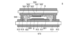
- Reference numeral 815 denotes a heat dissipating conductor layer of the substrate 810. It is sectional drawing which shows the semiconductor module 9 which concerns on a prior application.
- Reference numeral 913 indicates a third conductor layer
- reference numeral 915 indicates a heat dissipation conductor layer of the first substrate 910
- reference numeral 916 indicates a groove
- reference numeral 935 indicates a heat dissipation conductor layer of the second substrate 930.
- Reference numeral 937 indicates a flat portion
- reference numeral S indicates solder.
- the semiconductor module 1 according to Embodiment 1 includes a first substrate 10, a power device unit, a second substrate 30, an inner resin unit 40, A control IC 50, an outer resin portion 60, and a connector (connection member) 70 are provided, and the first substrate 10, the power device portion, the second substrate 30, and the control IC 50 are stacked in this order.
- the first substrate 10 includes a first insulating substrate 11, a first conductor layer 12 provided on one surface of the first insulating substrate 11, and a surrounding wall described later at a position separated from the first conductor layer 12.
- a fourth conductor layer 13 bonded to the portion 34, a conductor layer 14 for external connection provided at a position separated from the first conductor layer 12 and the fourth conductor layer 13, and a first insulating substrate 11 is a mounting board having a heat-dissipating conductor layer 15 provided on the other surface of 11.
- the first insulating substrate 11 is made of ceramics (for example, alumina), the first conductor layer 12, the fourth conductor layer 13, the external connection conductor layer 14, and the heat dissipation conductor layer. 15 is made of metal (for example, copper).
- the first substrate 10 is a DCB substrate (Direct Copper Bonding substrate) in which the first insulating substrate 11 and each conductor layer are bonded by eutectic bonding. By setting it as such a structure, it becomes a semiconductor module which has high heat dissipation.
- the fourth conductor layer 13 is formed with a groove 16 for engaging with a surrounding wall 34 described later.
- the groove portion 16 is formed by etching the fourth conductor layer.
- the external connection conductor layer 14 is not partially covered by the outer resin portion 60 or is connected to an external connection terminal (not shown), whereby an external circuit (not shown). ).
- the external connection conductor layer 14 is electrically connected to an input terminal (or control signal output terminal) of the control IC 50 via a third conductor layer 35 and a wire 80 described later.
- the power device section is composed of one semiconductor element 20, has a first electrode 21 on one side (lower side in FIG. 1), and a second electrode 22 and a gate electrode 23 on the other side (upper side in FIG. 1).
- the power device portion is arranged so that the entire semiconductor element 20 is located inside a region defined by the surrounding wall portion 34 in plan view.
- the semiconductor element 20 is a three-terminal semiconductor element (for example, IGBT).
- the gate electrode 23 is electrically connected to the control signal output terminal 52 of the control IC 50 through the connector 70.
- the first electrode 21 is electrically connected to the first conductor layer 12 and the second electrode 22 is bonded to a bonding portion 33 of the second substrate 30 to be described later via a bonding material S (for example, solder). It is connected to the.
- a bonding material S for example, solder
- the second substrate 30 includes a second insulating substrate 31, a second conductor layer 32 provided on one surface of the second insulating substrate 31, and the second insulating substrate 31. It has the 3rd conductor layer 35 provided in the other side.
- the second insulating substrate 31 is made of ceramics (for example, alumina), and the second conductor layer 32 and the third conductor layer 35 are made of metal (for example, copper).
- the second substrate 30 is a DCB substrate in which the second insulating substrate 31 and each conductor layer are bonded by eutectic bonding.
- the second insulating substrate 31 (and the second conductor layer 32 and the third conductor layer 35) has a hole 36 provided at a position corresponding to the position of the gate electrode 23.
- the second conductor layer 32 has a joint portion 33 joined to the second electrode 22, and an upper end surface at a position surrounding the joint portion 33 in a plan view and the second electrode 22 and the joint portion 33.
- the surrounding wall part 34 and the flat part 37 which were formed in the state which protruded rather than the joint surface with are included.
- the second substrate 30 is in contact with the first substrate 10 through the surrounding wall portion 34.
- the joint portion 33 and the surrounding wall portion 34 are formed by etching one copper layer. By setting it as such a structure, the junction part 33 and the surrounding wall part 34 can be formed accurately.
- the surrounding wall portion 34 is formed at a position surrounding the joint portion 33 over the entire circumference in plan view (see FIG. 1B). That is, the shape of the surrounding wall portion 34 is a “B” shape in plan view.
- the surrounding wall portion 34 is formed in a state of being continuous with the joint portion 33 through the flat portion 37 of the second conductor layer 32.
- the surrounding wall portion 34 is engaged with the groove portion 16 of the fourth conductor layer 13 of the first substrate 10 and is bonded via a bonding material (for example, solder).
- a bonding material for example, solder
- the length from the boundary surface between the second insulating substrate 31 and the second conductor layer 32 to the upper end surface of the surrounding wall portion 34 is, for example, in the range of 0.2 to 1.0 mm.
- the thickness of the joint portion 33 is, for example, in the range of 0.15 to 0.5 mm.
- the inner resin portion 40 is made of resin disposed in “a space defined by the surrounding wall portion 34 and sandwiched between the first insulating substrate 11 and the second insulating substrate 31”.
- An appropriate resin for example, epoxy resin
- the control IC 50 controls driving of the power device unit by controlling on / off of the gate electrode 23 of the power device unit.
- the control IC 50 is disposed on the third conductor layer 35.
- the control IC 50 has a predetermined control signal output terminal 52, and the control signal output terminal 52 and the gate electrode 23 are electrically connected via a connector 70 described later.
- the outer resin portion 60 is made of a resin disposed on one surface side of the first substrate 10 so as to cover at least the second substrate 30 and the control IC 50.
- the resin constituting the outer resin part 60 the same resin as that of the inner resin part 40 is used, but a different resin can also be used.
- the connector (connecting member) 70 is disposed inside the hole 36 of the second insulating substrate 31.
- the connector 70 has an elongated columnar shape, one end is electrically connected to the gate electrode 23 of the power device unit, and the other end is electrically connected to the control signal output terminal 52 of the control IC 50. Yes.
- the connector 70 is formed by punching / bending a metal plate. An appropriate material (for example, aluminum) can be used as the material of the metal plate.
- the semiconductor module 1 according to Embodiment 1 is a semiconductor module that satisfies the demand for product miniaturization.
- the second insulating substrate 31 has the hole 36 provided at a position corresponding to the position of the gate electrode 23, and the hole 36 of the second insulating substrate 31. Is connected to the control signal output terminal 52 of the control IC 50 via the connector 70, so that the control IC 50 is connected to the third conductor layer 35. Even in the case of being disposed above, the power device unit can be controlled by the control IC 50 without being obstructed by the second insulating substrate 31.
- the connector 70 is disposed inside the hole 36 of the second insulating substrate 31, and the gate electrode 23 is connected to the control signal of the control IC 50 via the connector 70. Since it is electrically connected to the output terminal 52, the length of the wiring (the length of the connector 70) between the gate electrode 23 of the power device section and the control signal output terminal 52 of the control IC 50 can be shortened. Less susceptible to external noise.
- the second conductor layer 32 has the surrounding wall portion 34 formed at a position surrounding the joint portion 33 in a plan view, so that an excessive load is applied to the power device portion. Even when the inner resin portion 40 is ignited by the heat generated when the fire is applied, it is possible to prevent the surrounding fire from spreading by the surrounding wall portion 34 serving as a fire barrier.
- the second conductor layer 32 has the surrounding wall portion 34 formed at a position surrounding the joint portion 33 in a plan view, so that the power device portion is surrounded by the outside. It can be shielded by the wall 34 and can prevent the power device unit from oscillating or malfunctioning due to noise from the outside of the power device unit. As a result, the semiconductor module 1 according to the first embodiment The semiconductor module is less likely to malfunction due to malfunction.
- the surrounding wall portion 34 is formed at a position that surrounds the joint portion 33 over the entire circumference in plan view, and therefore when an excessive load is applied to the power device portion. Even when the inner resin portion 40 is ignited by the heat generation, the surrounding wall portion 34 completely surrounds the inner resin portion 40, so that it is possible to reliably prevent the surrounding fire from spreading. Further, since the power device portion can be completely shielded from the outside by the surrounding wall portion 34, it is possible to reliably prevent the power device portion from oscillating or malfunctioning due to noise from the outside of the power device portion.
- the surrounding wall portion 34 is formed in a state of being continuous with the joint portion 33, and the first substrate 10 is connected to the first conductor layer 12 on one surface of the second insulating substrate 31.
- the fourth conductor layer 13 is further joined to the surrounding wall portion 34 at a spaced position, and the fourth conductor layer 13 is electrically connected to the second electrode 22 via the surrounding wall portion 34 and the joining portion 33. It is connected.
- the second electrode 22 of the power device portion can be electrically connected to the outside through the joint portion 33, the surrounding wall portion 34, and the fourth conductor layer 13.
- junction part 33, the surrounding wall part 34, and the 4th conductor layer 13 have a cross-sectional area larger than a wire and resistance is low, it is hard to produce a malfunction when a big electric current is sent through a semiconductor module, and much higher reliability. It becomes a semiconductor module having properties.
- the semiconductor module 1 since it has the above-described configuration, heat generated in the power device portion is radiated to the outside via the joint portion 33, the surrounding wall portion 34, and the fourth conductor layer 13. Thus, a semiconductor module having even higher heat dissipation can be obtained.
- the surrounding wall portion 34 of the second substrate 30 can be easily positioned by fitting into the groove portion 16 of the fourth conductor layer 13.
- the power device unit includes the single semiconductor element 20, and the semiconductor element 20 has the first electrode 21 on one side and the second side on the other side. Since it has the electrode 22 and the gate electrode 23, it becomes a semiconductor module with a simple wiring design.
- the joint portion 33 and the surrounding wall portion 34 are formed from one copper layer, a joint material (for example, solder) is used in the manufacturing process of the semiconductor module. Even when it is put in a high-temperature furnace to melt it, the length of the surrounding wall 34 hardly changes. Accordingly, since the load of the second substrate 30 is distributed to the surrounding wall portion 34, the load of the second substrate 30 does not concentrate on the power device portion. As a result, the power device part is less likely to be broken in the manufacturing process of the semiconductor module, so that not only the semiconductor module with a high yield is obtained, but also when it is put in a high temperature furnace to melt the bonding material (for example, solder). The thickness of the bonding material can be prevented from changing, and a highly reliable semiconductor module can be obtained.
- a joint material for example, solder
- the joint portion 33 and the surrounding wall portion 34 are formed from one copper layer, the surrounding wall portion 34 is not inclined, In the manufacturing process of the semiconductor module, the second substrate 30 can be accurately positioned without the second substrate 30 rotating in the ⁇ direction in plan view.
- the semiconductor module 2 according to the second embodiment basically has the same configuration as the semiconductor module 1 according to the first embodiment, but the configuration of the surrounding wall portion is different from that of the semiconductor module 1 according to the first embodiment. That is, in the semiconductor module 2 according to the second embodiment, as shown in FIG. 3, the surrounding wall portion 34 is a predetermined portion of the position surrounding the joint portion 33 in plan view (over the 3/4 circumference of the joint portion 33). It is formed only at the surrounding position (see FIG. 3B). That is, the shape of the surrounding wall portion 34 is a “U” shape in plan view.
- the semiconductor module 2 according to the second embodiment is different from the semiconductor module 1 according to the first embodiment in the configuration of the surrounding wall portion, but as in the case of the semiconductor module 1 according to the first embodiment, Since the first substrate 10, the power device unit (semiconductor element 20), the second substrate 30a, and the control IC 50 are stacked in this order, the first insulating property is provided even when the control IC 50 that controls the power device unit is provided. It is not necessary to secure a region for installing the control IC 50 on one side of the substrate 11, and the occupation area is made narrower than when the control IC 50 is installed side by side with the power device unit on the one side of the first insulating substrate 11. Can do. As a result, the semiconductor module 2 according to the second embodiment is a semiconductor module that satisfies the demand for product miniaturization.
- the surrounding wall portion 34a is formed only in a predetermined portion of the position surrounding the joint portion 33 in plan view, and thus forms the inner resin portion 40.
- a space sandwiched between the first insulating substrate 11 and the second insulating substrate 31 at a position where the surrounding wall portion 34 is not formed in a position surrounding the joint portion 33 in plan view Resin can be injected.
- the semiconductor module 2 according to the second embodiment has the same configuration as the semiconductor module 1 according to the first embodiment except for the configuration of the surrounding wall portion, the effects of the semiconductor module 1 according to the first embodiment can be obtained. Of which, it has a corresponding effect.
- the semiconductor module 3 according to the third embodiment basically has the same configuration as the semiconductor module 1 according to the first embodiment, but the configuration of the power device unit is different from that of the semiconductor module 1 according to the first embodiment. That is, in the semiconductor module 3 according to the third embodiment, the power device unit has a structure in which two semiconductor elements 20a and 20b are stacked as shown in FIG.
- the power device unit has a structure in which a three-terminal semiconductor element 20a is stacked on a two-terminal semiconductor element 20b.
- the three-terminal semiconductor element 20a has a first electrode 21a formed on one side (lower side) electrically connected to a second electrode 22b of the semiconductor element 20b, and is formed on the other side (upper side).
- the second electrode 22a is electrically connected to the three-terminal joint 33a
- the gate electrode 23a is electrically connected to the control signal output terminal 52 of the control IC 50 via the connector 70.
- the first electrode 21b formed on one side (lower side) is electrically connected to the first conductor layer 12, and the second electrode formed on the other side (upper side).
- the electrode 22b is electrically connected to the first electrode 21a of the three-terminal semiconductor element 20a.
- the configuration of the power device unit is different from that of the semiconductor module 1 according to the first embodiment. Since the first substrate 10, the power device unit (semiconductor elements 20a, 20b), the second substrate 30, and the control IC 50 are stacked in this order, even if the control IC 50 for controlling the power device unit is provided, the first There is no need to secure a region for installing the control IC 50 on one side of the insulating substrate 11, and the occupied area is smaller than when the control IC 50 is installed side by side with the power device unit on the one side of the first insulating substrate 11. can do. As a result, the semiconductor module 3 according to the third embodiment is a semiconductor module that satisfies the demand for product miniaturization.
- the power device unit has a structure in which the two semiconductor elements 20a and 20b are stacked, so that the two semiconductor elements 20a and 20b are connected to the first insulating substrate 11. Occupied area can be made narrower than when arranged side by side on one side. As a result, the semiconductor module satisfies a high level of demand for product miniaturization.
- the semiconductor module 3 according to the third embodiment has the same configuration as that of the semiconductor module 1 according to the first embodiment except for the configuration of the power device unit, the effects of the semiconductor module 1 according to the first embodiment can be obtained. Of which, it has a corresponding effect.
- the semiconductor module 4 according to the fourth embodiment basically has the same configuration as the semiconductor module 3 according to the third embodiment, but is different from the case of the semiconductor module 3 according to the third embodiment in that it includes a second connection member. Different. That is, in the semiconductor module 4 according to the fourth embodiment, as shown in FIG. 5, one end is sandwiched between two semiconductor elements 20a and 20b, and the other end is a fifth conductor layer 17 described later. And a second connection member 82 that is electrically connected to the first connection member 82.
- the second connecting member 82 is formed by punching / bending a metal plate (for example, an aluminum plate).
- One end of the second connection member 82 is slightly larger than the two semiconductor elements 20a and 20b in plan view, and the upper side (second substrate side) of the one end is joined to the first electrode 21a of the semiconductor element 20a. Bonded via a material (solder), the lower side (first substrate side) of one end is bonded to the second electrode 22b of the semiconductor element 20b via a bonding material (solder).
- the first substrate 10 further includes a fifth conductor layer 17 provided at a position separated from both the first conductor layer 12 and the external connection conductor layer 14.
- the fifth conductor layer 17 is not partially covered by the outer resin portion 60 or connected to an external connection terminal (not shown), thereby causing an external circuit (not shown). Connected with.
- the surrounding wall portion 34b is formed only in a predetermined portion (a position surrounding the 3 ⁇ 4 circumference of the joint portion 33) in a position surrounding the joint portion 33b in a plan view (see FIG. 5B). That is, the shape of the surrounding wall portion 34b is a “U” shape in plan view.
- the second connecting member 82 is “a space sandwiched between the first insulating substrate 11 and the second insulating substrate 31 b at a position where the surrounding wall portion 34 b is not formed in a position surrounding the joint portion 33 b in a plan view. To pass through.
- the semiconductor module 4 according to the fourth embodiment is different from the semiconductor module 3 according to the third embodiment in that the second connection member is provided, but similarly to the semiconductor module 3 according to the third embodiment. Since the first substrate 10, the power device unit (semiconductor elements 20a and 20b), the second substrate 30b, and the control IC 50 are stacked in this order, the control IC 50 that controls the power device unit is provided. There is no need to secure a region for installing the control IC 50 on one side of the first insulating substrate 11, and the occupied area is larger than when the control IC 50 is installed side by side with the power device unit on one side of the first insulating substrate 11. Can be narrowed. As a result, the semiconductor module 4 according to the fourth embodiment is a semiconductor module that satisfies the demand for product miniaturization.
- the semiconductor module 4 according to the fourth embodiment, one end is sandwiched between the two semiconductor elements 20a and 20b, and the other end is electrically connected to the fifth conductor layer 17. Since the second connecting member 82 is provided, the semiconductor module has a higher degree of design freedom.
- the semiconductor module 4 according to the fourth embodiment has the same configuration as that of the semiconductor module 3 according to the third embodiment except that the semiconductor module 4 according to the fourth embodiment includes the second connection member. It has a corresponding effect among the effects.
- the semiconductor module 5 according to the fifth embodiment basically has the same configuration as the semiconductor module 3 according to the third embodiment, but the configuration of the power device unit is different from that of the semiconductor module 3 according to the third embodiment. That is, in the semiconductor module 5 according to the fifth embodiment, the two semiconductor elements 20a and 20c (the semiconductor element on the second substrate side is 20a and the semiconductor element on the first substrate side is 20c) are all shown in FIG. As shown, the first electrodes 21a and 21c are provided on one side, and the second electrodes 22a and 22c and the two gate electrodes 23a and 23c are provided on the other side.
- the two semiconductor elements 20a and 20c are both laminated so that the entire semiconductor element is located inside the region defined by the surrounding wall portion 34 in plan view.
- the second insulating substrate 31 has holes corresponding to the gate electrodes 23a and 23c of the two semiconductor elements 20a and 20c, and the connectors 70a and 70c are arranged inside the holes.
- the configuration of the power device unit is different from that in the semiconductor module 3 according to the third embodiment. Since the first substrate 10, the power device unit (semiconductor elements 20a and 20c), the second substrate 30, and the control IC 50 are stacked in this order, even if the control IC 50 for controlling the power device unit is provided, the first There is no need to secure a region for installing the control IC 50 on one side of the insulating substrate 11, and the occupied area is smaller than when the control IC 50 is installed side by side with the power device unit on the one side of the first insulating substrate 11. can do. As a result, the semiconductor module 5 according to the fifth embodiment is a semiconductor module that satisfies the demand for product miniaturization.
- the two semiconductor elements 20a and 20c are stacked such that the entire semiconductor element is positioned inside the region defined by the surrounding wall portion 34 in plan view. Therefore, the two semiconductor elements 20a and 20c can be completely shielded from the outside by the surrounding wall portion 34, and as a result, the two semiconductor elements 20a and 20c may oscillate or malfunction due to external noise. It can be surely prevented.
- the semiconductor module 5 according to the fifth embodiment has the same configuration as that of the semiconductor module 3 according to the third embodiment except for the configuration of the power device unit, the effects of the semiconductor module 3 according to the third embodiment can be obtained. Of which, it has a corresponding effect.
- the semiconductor module 6 according to the sixth embodiment basically has the same configuration as the semiconductor module 5 according to the fifth embodiment, but the configuration of the power device unit is different from that of the semiconductor module 5 according to the fifth embodiment. That is, in the semiconductor module 6 according to the sixth embodiment, one of the two semiconductor elements (the lower semiconductor element 20c) is a region defined by the surrounding wall 34c in plan view, as shown in FIG. The gate electrode 23c of the semiconductor element 20c is stacked on the outside of the semiconductor element 20c.
- the semiconductor module 6 according to Embodiment 6 has a second connection in which one end is sandwiched between the two semiconductor elements 20 a and 20 c and the other end is electrically connected to the fifth conductor layer 17.
- a member 82 is further provided.
- One end of the second connection member 82 is slightly larger than the semiconductor elements 20a and 20c in a plan view, and the upper side (second substrate side) of the one end is the first electrode 21a of the semiconductor element 20a and a bonding material ( The first electrode 22c is bonded to the second electrode 22c of the semiconductor element 20c via a bonding material (solder).
- the surrounding wall portion 34c is formed only at a predetermined position (a position surrounding the joint portion 33 over a half circumference in the plan view) among positions surrounding the joint portion 33c in the plan view (see FIG. 7B). That is, the shape of the surrounding wall portion 34c is an “L” shape in plan view.
- the gate electrode 23c of the (lower) semiconductor element 20c is electrically connected via a wire 80 to a control signal output terminal 52b of a control IC 50b provided at a position separated from the surrounding wall 34c.
- the gate electrode 23c In a predetermined direction perpendicular to the outer edge of the surrounding wall portion 34c, the gate electrode 23c is separated from the outer edge of the region defined by the surrounding wall portion 34c in plan view by a factor of three times the width of the gate electrode 23c in the predetermined direction. It is preferable. By adopting such a configuration, the linear distance between the wire 80 connecting the gate electrode 23c and the control signal output terminal 52c of the control IC 50b and the surrounding wall portion 34c becomes long, and short-circuiting is difficult.
- the configuration of the power device unit is different from that in the semiconductor module 5 according to the fifth embodiment, but as in the case of the semiconductor module 5 according to the fifth embodiment, Since the one substrate 10, the power device unit (semiconductor elements 20a and 20c), the second substrate 30c, and the control IC 50a are stacked in this order, the first IC 10a is provided even if the control IC 50a for controlling the power device unit is provided. It is not necessary to secure a region for installing the control IC 50a on one side of the insulating substrate 11, and the occupied area is narrower than when the control IC 50a is installed side by side with the power device unit on the one side of the first insulating substrate 11. can do. As a result, the semiconductor module 6 according to the sixth embodiment is a semiconductor module that satisfies the demand for product miniaturization.
- the semiconductor module 6 according to the sixth embodiment since the gate electrode 23c of the semiconductor element 20c is positioned outside the region defined by the surrounding wall portion 34c in plan view, the power device portion Even when the second substrate 30c is provided in the uppermost part, the gate electrode 23c of the power device unit and the control signal output terminal 52b of the control IC 50b can be connected by the wire 80 having a small diameter.
- the semiconductor module 6 according to the sixth embodiment is a semiconductor module capable of controlling the power device unit (the semiconductor element 20b below the power device unit) with the control IC 50b.
- the semiconductor module 6 according to the sixth embodiment has the same configuration as that of the semiconductor module 5 according to the fifth embodiment except for the configuration of the power device unit, the effect of the semiconductor module 5 according to the fifth embodiment is obtained. Of which, it has a corresponding effect.
- the semiconductor module 7 according to the seventh embodiment basically has the same configuration as that of the semiconductor module 1 according to the first embodiment, but the configuration of the surrounding wall portion is different from that of the semiconductor module 1 according to the first embodiment. That is, in the semiconductor module 7 according to the seventh embodiment, the surrounding wall portion 34d is formed in a state of being separated from the joint portion 33d as shown in FIG.
- the first substrate 10 further includes a fourth conductor layer 13 joined to the surrounding wall portion 34d at a position separated from the first conductor layer 12 on one surface of the first insulating substrate 11, and the fourth conductor
- the layer 13 is formed with a groove portion 16 for engaging with the surrounding wall portion 34d.
- the semiconductor module 7 according to the seventh embodiment is different from the semiconductor module 1 according to the first embodiment in the configuration of the surrounding wall portion, but as in the case of the semiconductor module 1 according to the first embodiment, Since the first substrate 10, the power device unit (semiconductor element 20), the second substrate 30d, and the control IC 50 are stacked in this order, the first insulating property is provided even when the control IC 50 that controls the power device unit is provided. It is not necessary to secure a region for installing the control IC 50 on one side of the substrate 11, and the occupation area is made narrower than when the control IC 50 is installed side by side with the power device unit on the one side of the first insulating substrate 11. Can do. As a result, the semiconductor module 7 according to the seventh embodiment is a semiconductor module that satisfies the demand for product miniaturization.
- the surrounding wall portion 34d is formed in a state of being separated from the joint portion 33d, and therefore, with other conductor layers and semiconductor elements via the surrounding wall portion 34d. It is possible to prevent a short circuit and a semiconductor module that is difficult to be destroyed.
- the semiconductor module 7 according to the seventh embodiment has the same configuration as that of the semiconductor module 1 according to the first embodiment except for the configuration of the surrounding wall portion, the effects of the semiconductor module 1 according to the first embodiment can be obtained. Of which, it has a corresponding effect.
- the power device section has a structure in which two semiconductor elements are stacked, but the present invention is not limited to this.
- the power device unit may have a structure in which three or more semiconductor elements are stacked.
- the two semiconductor elements are stacked while being shifted by 90 °, but the present invention is not limited to this. Two semiconductor elements may be stacked in a state shifted by an angle other than 90 °.
- the first substrate is a DCB substrate, but the present invention is not limited to this.
- the first substrate may be a general printed board or an aluminum board.
- the second substrate is a DCB substrate, but the present invention is not limited to this.
- the second substrate may be a general printed board or an aluminum board.
- the heat dissipating conductor layer is provided on the other surface side of the first substrate, but the present invention is not limited to this.
- the heat dissipating conductor layer may not be provided.
- the joint portion and the surrounding wall portion are formed by etching one conductor layer, but the present invention is not limited to this.
- the joint portion and the surrounding wall portion may be separately formed and then joined to the second insulating substrate 31 to form the joint portion and the surrounding wall portion.
- the groove portion for engaging with the surrounding wall portion is formed in the fourth conductor layer, but the present invention is not limited to this.
- the groove portion may not be formed in the fourth conductor layer.
- gate electrode 30, 30a, 30b, 30c, 30d ... second substrate , 31 ... second insulating substrate, 32, 32a, 32b, 32c, 32d ... second conductor layer, 33, 33a, 33b, 33c, 33d ... junction, 34, 34a, 34b, 34c, 34d ... surrounding wall Part, 35 ... third conductor layer, 36 ... hole, 37 ... flat part, 4 ... inner resin part, 50, 50a, 50b ... control IC, 52, 52a, 52b ... control signal output terminal, 60 ... outer resin part, 70 ... connector (for gate electrode connection), 80 ... wire, 82 ... first 2 connecting members, S ... bonding material
Landscapes
- Cooling Or The Like Of Semiconductors Or Solid State Devices (AREA)
- Engineering & Computer Science (AREA)
- Structures Or Materials For Encapsulating Or Coating Semiconductor Devices Or Solid State Devices (AREA)
- Inverter Devices (AREA)
- Chemical & Material Sciences (AREA)
- Ceramic Engineering (AREA)
- Physics & Mathematics (AREA)
- Health & Medical Sciences (AREA)
- Electromagnetism (AREA)
- Toxicology (AREA)
- Production Of Multi-Layered Print Wiring Board (AREA)
- Microelectronics & Electronic Packaging (AREA)
Abstract
本発明の半導体モジュール1は、第1絶縁性基板11及び第1導電体層12を有する第1基板10と、第1電極21、第2電極22及びゲート電極23を有するパワーデバイス部20と、第2絶縁性基板31、第2導電体層32及び第3導電体層35を有し、第2絶縁性基板31が、孔36を有し、第2導電体層32が、接合部33及び囲繞壁部34を有する第2基板30と、内側樹脂部40と、制御IC50と、外側樹脂部60とを備え、第1基板10、パワーデバイス部20、第2基板30及び制御IC50がこの順序で積層され、孔36の内側には接続部材70が配置され、ゲート電極23は、接続部材70を介して制御IC50の制御信号出力端子52に電気的に接続されている。 本発明のパワー半導体装置1は、パワーデバイス部を制御する制御ICを備える場合であっても、製品の小型化の要請を満たす半導体モジュールとなる。
Description
本発明は、半導体モジュールに関する。
従来、基板と半導体素子とを備える半導体モジュールが知られている(例えば、特許文献1参照。)。
従来の半導体モジュール8は、図9に示すように、絶縁性基板811、絶縁性基板811の一方面に設けられた導電体層812及び導電体層812とは離間した位置に設けられた他の導電体層813,814を有する基板810と、一方面(図9の下側の面)に第1電極821を有し他方面(図9の上側の面)に2つの第2電極822,823を有し、第1電極821が導電体層812に接合されたデバイス部(半導体素子)820と、絶縁性基板811の外周に沿って形成された壁部816と、絶縁性基板811と壁部816とで構成される升状の空間に樹脂を配置することにより形成された樹脂部860と、樹脂部860の上面に配置された樹脂製の蓋部862と、一方端が他の導電体層813,814と電気的に接続され、かつ、当該一方端から樹脂部860及び蓋部862を介して外部(鉛直上方)に向かって延出された外部接続用の端子874,876とを備える。
半導体素子820の2つの第2電極822,823のうち、一方の第2電極822は、ワイヤ870及び他の導電体層813を介して端子874と電気的に接続され、他方の第2電極823は、ワイヤ872を介して端子876と電気的に接続されている。
従来の半導体モジュール8は、基板810と壁部816とで構成される升状の空間に樹脂を配置することにより形成された樹脂部860を備えるため、耐衝撃性を有する半導体モジュールとなる。
ところで、近年、半導体モジュールの技術の分野においては、樹脂封止するための構造を容易に形成することができる半導体モジュールが求められている。
そこで、本発明の発明者らは、樹脂封止するための構造を容易に形成することができる半導体モジュールを想到し、PCT/JP2015/051655(以下、先願という。)として既に出願している。
先願に係る半導体モジュール9は、図10に示すように、第1絶縁性基板911及び第1絶縁性基板911の少なくとも一方面に設けられた第1導電体層912を有する第1基板910と、一方面に第1電極921を有し、かつ、他方面に第2電極922を有し、第1電極921が第1導電体層912に接合されたデバイス部(半導体素子)920と、第2絶縁性基板931及び第2絶縁性基板931の少なくとも一方面に設けられた第2導電体層932を有し、第2導電体層932が、第2電極922と接合する接合部933及び平面視において接合部933を取り囲む位置に上端面が接合部933と第2電極922との接合面よりも突出した状態で形成された囲繞壁部934を有し、囲繞壁部934を介して第1基板910と接している第2基板930と、囲繞壁部934によって画定され、かつ、第1絶縁性基板911及び第2絶縁性基板931に挟まれた空間に配置された樹脂からなる樹脂部940とを備える。
先願に係る半導体モジュール9においては、平面視において囲繞壁部934によって画定された領域の内側にデバイス部920全体が位置するようにデバイス部920が配置されている。
先願に係る半導体モジュール9によれば、第2導電体層932が平面視において接合部933を取り囲む位置に、かつ、上端面が接合部933と第2電極922との接合面よりも上に突出した状態で形成されている囲繞壁部934を有するため、樹脂封止するための構造を形成するための部材(例えば、従来の半導体モジュール8における壁部816)を別途準備する必要がなく、樹脂封止するための構造を容易に形成することができる。
また、先願に係る半導体モジュール9によれば、デバイス部920の第2電極922が、第2絶縁性基板931の一方面に設けられた第2導電体層932に接合されているため、デバイス部920で発生した熱を第1導電体層912及び第1絶縁性基板911を介して外部へ放熱するのに加えて、第2導電体層932及び第2絶縁性基板931を介して外部へ放熱することができる。従って、先願に係る半導体モジュール9は、従来よりも高い放熱性を有する半導体モジュールとなる。
ところで、近年の半導体モジュールの技術の分野においては、製品の小型化の要請を満たす半導体モジュールが求められている。しかしながら、このような半導体モジュールにおいて、デバイス部としてゲート電極を有するパワーデバイス部(パワー半導体素子)を用い、パワーデバイス部を制御する制御ICを第1絶縁性基板の一方面側に設置する場合、第1絶縁性基板の一方面側に制御ICを設置する領域を確保する必要があり、占有面積が広くなるため、製品の小型化の要請を満たす半導体モジュールとすることができない、という問題がある。
そこで、本発明は、上記した問題を解決するためになされたものであり、パワーデバイス部を制御する制御ICを備える場合であっても、製品の小型化の要請を満たす半導体モジュールを提供することを目的とする。
[1]本発明の半導体モジュールは、第1絶縁性基板及び前記第1絶縁性基板の一方面に設けられた第1導電体層を有する第1基板と、一方面に第1電極を有し、かつ、他方面に第2電極及びゲート電極を有し、前記第1電極が前記第1導電体層に電気的に接続されているパワーデバイス部と、第2絶縁性基板、前記第2絶縁性基板の一方面に設けられた第2導電体層及び前記第2絶縁性基板の他方面に設けられた第3導電体層を有し、前記第2絶縁性基板が、前記ゲート電極の位置に対応する位置に設けられた孔を有し、前記第2導電体層が、前記第2電極と接合する接合部及び平面視において前記接合部を取り囲む位置に上端面が前記第2電極と前記接合部との接合面よりも突出した状態で形成された囲繞壁部を有し、前記囲繞壁部を介して前記第1基板と接している第2基板と、前記囲繞壁部によって画定され、かつ、前記第1絶縁性基板及び前記第2絶縁性基板に挟まれた空間に配置された樹脂からなる内側樹脂部と、前記第3導電体層上に配置された制御ICと、前記第1基板の一方面側に、前記第2基板及び前記制御ICを覆うように配置された樹脂からなる外側樹脂部とを備え、前記第1基板、前記パワーデバイス部、前記第2基板及び前記制御ICがこの順序で積層された半導体モジュールであって、前記第2絶縁性基板の孔の内側には接続部材が配置され、前記ゲート電極は、前記接続部材を介して前記制御ICの制御信号出力端子に電気的に接続されていることを特徴とする。
なお、本明細書中、「接合部を取り囲む位置に・・・形成された囲繞壁部」とは、平面視において接合部を全周にわたって取り囲む位置に囲繞壁部が形成されている場合のみならず、接合部を取り囲む位置のうちの所定の部分のみに囲繞壁部が形成されている場合も含む。
[2]本発明の半導体モジュールにおいては、前記囲繞壁部は、平面視において前記接合部を全周にわたって取り囲む位置に形成されていることが好ましい。
[3]本発明の半導体モジュールにおいては、前記囲繞壁部は、平面視において前記接合部を取り囲む位置のうちの所定の部分のみに形成されていることが好ましい。
[4]本発明の半導体モジュールにおいては、前記囲繞壁部は、前記接合部と連続した状態で形成され、前記第1基板は、前記第1絶縁性基板の一方面における前記第1導電体層と離間した位置で前記囲繞壁部と接合される第4導電体層をさらに有し、前記第4導電体層は、前記囲繞壁部及び前記接合部を介して前記第2電極と電気的に接続されていることが好ましい。
なお、本明細書中、「囲繞壁部は、接合部と連続した状態で形成され」とは、囲繞壁部が、接合部と隣り合っている場合のみならず、囲繞壁部と接合部との間に別の部材が挟まれている場合も含む。
[5]本発明の半導体モジュールにおいては、前記第4導電体層には、前記囲繞壁部と係合するための溝部が形成されていることが好ましい。
[6]本発明の半導体モジュールにおいては、前記囲繞壁部は、前記接合部と離間した状態で形成されていることが好ましい。
[7]本発明の半導体モジュールにおいては、前記第1基板は、前記第1絶縁性基板の一方面における前記第1導電体層と離間した位置で前記囲繞壁部と接合される第4導電体層をさらに有し、前記第4導電体層には、前記囲繞壁部と係合するための溝部が形成されていることが好ましい。
[8]本発明の半導体モジュールにおいては、前記パワーデバイス部は、1つの半導体素子からなり、前記1つの半導体素子は、一方面に第1電極を有し、かつ、他方面に第2電極及びゲート電極を有することが好ましい。
[9]本発明の半導体モジュールにおいては、前記パワーデバイス部は、複数の半導体素子が積層された構造を有し、前記複数の半導体素子のうち少なくとも1つの半導体素子は、一方面に第1電極を有し、かつ、他方面に第2電極及びゲート電極を有することが好ましい。
なお、本明細書において、2つ以上の半導体素子がゲート電極を有する場合、各ゲート電極がそれぞれ接続部材と電気的に接続できるようにずらした状態で半導体素子が積層されている。
[10]本発明の半導体モジュールにおいては、前記パワーデバイス部は、複数の半導体素子が積層された構造を有し、前記第1基板は、前記第1導電体層と離間した位置に設けられている第5導電体層をさらに有し、前記半導体モジュールは、一方端が前記複数の半導体素子のうちの2つの半導体素子の間に挟まれており、かつ、他方端が前記第5導電体層と電気的に接続されている第2接続部材をさらに備えることが好ましい。
[11]本発明の半導体モジュールにおいては、前記パワーデバイス部は、複数の半導体素子が積層された構造を有し、前記複数の半導体素子のうち少なくとも2つの半導体素子はいずれも、一方面に第1電極を有し、かつ、他方面に第2電極及びゲート電極を有し、前記少なくとも2つの半導体素子はいずれも、平面視において前記囲繞壁部によって画定された領域の内側に半導体素子全体が位置するように積層されていることが好ましい。
[12]本発明の半導体モジュールにおいては、前記パワーデバイス部は、複数の半導体素子が積層された構造を有し、前記複数の半導体素子のうち少なくとも2つの半導体素子はいずれも、一方面に第1電極を有し、かつ、他方面に第2電極及びゲート電極を有し、前記少なくとも2つの半導体素子のうちの少なくとも1つは、平面視において前記囲繞壁部によって画定された領域の外側に前記半導体素子の前記ゲート電極が位置するように積層されていることが好ましい。
[13]本発明の半導体モジュールにおいては、前記接合部及び前記囲繞壁部は、1の銅層から形成されたものであることが好ましい。
本発明の半導体モジュールによれば、第1基板、パワーデバイス部、第2基板及び制御ICがこの順序で積層されているため、パワーデバイス部を制御する制御ICを備える場合であっても、第1絶縁性基板の一方面側に制御ICを設置する領域を確保する必要がなく、第1絶縁性基板の一方面側に制御ICをパワーデバイス部と並べて設置した場合よりも占有面積を狭くすることができる。その結果、本発明の半導体モジュールは、製品の小型化の要請を満たす半導体モジュールとなる。
また、本発明の半導体モジュールによれば、第2絶縁性基板が、ゲート電極の位置に対応する位置に設けられた孔を有し、第2絶縁性基板の孔の内側には接続部材が配置され、かつ、ゲート電極が接続部材を介して制御ICの制御信号出力端子に電気的に接続されているため、制御ICが第3導電体層上に配置されている場合であっても、第2絶縁性基板に邪魔されることなく制御ICでパワーデバイス部を制御することができる。
また、本発明の半導体モジュールによれば、第2絶縁性基板の孔の内側には接続部材が配置され、ゲート電極は、接続部材を介して制御ICの制御信号出力端子に電気的に接続されているため、パワーデバイス部のゲート電極と制御ICの制御信号出力端子との間の配線の長さ(接続部材の長さ)が短くて済み、外部からのノイズの影響を受けにくくなる。
また、本発明の半導体モジュールによれば、第2導電体層が、平面視において接合部を取り囲む位置に形成された囲繞壁部を有するため、パワーデバイス部に過大な負荷をかけたときの発熱によって内側樹脂部が発火した場合であっても、囲繞壁部が防火壁の役割を果たすことにより周囲への延焼を防ぐことができる。
また、本発明の半導体モジュールによれば、第2導電体層が、平面視において接合部を取り囲む位置に形成された囲繞壁部を有するため、パワーデバイス部を外部から囲繞壁部で遮蔽することができ、パワーデバイス部の外部からのノイズによってパワーデバイス部に発振又は誤動作が起こることを防ぐことができ、その結果、本発明の半導体モジュールは、発振又は誤動作による不具合が少ない半導体モジュールとなる。
以下、本発明の半導体モジュールについて、図に示す実施形態に基づいて説明する。
[実施形態1]
1.実施形態1に係る半導体モジュール1の構成
実施形態1に係る半導体モジュール1は、図1に示すように、第1基板10と、パワーデバイス部と、第2基板30と、内側樹脂部40と、制御IC50と、外側樹脂部60と、接続子(接続部材)70とを備え、第1基板10、パワーデバイス部、第2基板30及び制御IC50がこの順序で積層されている。
1.実施形態1に係る半導体モジュール1の構成
実施形態1に係る半導体モジュール1は、図1に示すように、第1基板10と、パワーデバイス部と、第2基板30と、内側樹脂部40と、制御IC50と、外側樹脂部60と、接続子(接続部材)70とを備え、第1基板10、パワーデバイス部、第2基板30及び制御IC50がこの順序で積層されている。
第1基板10は、第1絶縁性基板11と、第1絶縁性基板11の一方面に設けられた第1導電体層12と、第1導電体層12と離間した位置で後述する囲繞壁部34と接合される第4導電体層13と、第1導電体層12及び第4導電体層13とは離間した位置に設けられた外部接続用導電体層14と、第1絶縁性基板11の他方面に設けられた放熱用導電体層15とを有する実装基板である。
第1基板10において、第1絶縁性基板11は、セラミックス(例えば、アルミナ)からなり、第1導電体層12、第4導電体層13、外部接続用導電体層14及び放熱用導電体層15は、金属(例えば銅)からなる。第1基板10は、第1絶縁性基板11と各導電体層が共晶接合によって接合されているDCB基板(Direct Cupper Bonding基板)である。このような構成とすることにより、高い放熱性を有する半導体モジュールとなる。
第4導電体層13には、後述する囲繞壁部34と係合するための溝部16が形成されている。溝部16は第4導電体層をエッチングすることにより形成されたものである。外部接続用導電体層14は、一部が外側樹脂部60に覆われていないことにより又は外部接続用の端子(図示せず。)と接続されていることにより、外部回路(図示せず。)と接続されている。外部接続用導電体層14は、後述する第3導電体層35及びワイヤ80を介して制御IC50の入力端子(又は制御信号出力端子)と電気的に接続されている。
パワーデバイス部は、1つの半導体素子20からなり、一方面(図1の下側)に第1電極21を有し、かつ、他方面(図1の上側)に第2電極22及びゲート電極23を有する。パワーデバイス部は、平面視において囲繞壁部34によって画定された領域の内側に半導体素子20全体が位置するように配置されている。半導体素子20は、3端子の半導体素子(例えば、IGBT)である。
ゲート電極23は、接続子70を介して制御IC50の制御信号出力端子52と電気的に接続されている。第1電極21は第1導電体層12と、第2電極22は後述する第2基板30の接合部33と、それぞれ接合材S(例えば、はんだ)を介して接合されることにより、電気的に接続されている。
第2基板30は、図1及び図2に示すように、第2絶縁性基板31、第2絶縁性基板31の一方面に設けられた第2導電体層32及び第2絶縁性基板31の他方面に設けられた第3導電体層35を有する。第2基板30において、第2絶縁性基板31は、セラミックス(例えば、アルミナ)からなり、第2導電体層32及び第3導電体層35は、金属(例えば銅)からなる。第2基板30は、第2絶縁性基板31と各導電体層が共晶接合によって接合されているDCB基板である。
第2絶縁性基板31(及び第2導電体層32及び第3導電体層35)は、図2に示すように、ゲート電極23の位置に対応する位置に設けられた孔36を有する。
第2導電体層32は、図1及び図2に示すように、第2電極22と接合する接合部33、平面視において接合部33を取り囲む位置に上端面が第2電極22と接合部33との接合面よりも突出した状態で形成された囲繞壁部34及び平坦部37を有する。第2基板30は、囲繞壁部34を介して第1基板10と接している。なお、接合部33及び囲繞壁部34は、1の銅層をエッチングすることによって形成されたものである。このような構成とすることにより、接合部33及び囲繞壁部34を精度よく形成することができる。
第2導電体層32は、図1及び図2に示すように、第2電極22と接合する接合部33、平面視において接合部33を取り囲む位置に上端面が第2電極22と接合部33との接合面よりも突出した状態で形成された囲繞壁部34及び平坦部37を有する。第2基板30は、囲繞壁部34を介して第1基板10と接している。なお、接合部33及び囲繞壁部34は、1の銅層をエッチングすることによって形成されたものである。このような構成とすることにより、接合部33及び囲繞壁部34を精度よく形成することができる。
囲繞壁部34は、平面視において接合部33を全周にわたって取り囲む位置に形成されている(図1(b)参照。)。すなわち、囲繞壁部34の形状は、平面視において「ロ」の字形状をしている。
囲繞壁部34は、第2導電体層32の平坦部37を介して接合部33と連続した状態で形成されている。囲繞壁部34は、第1基板10の第4導電体層13の溝部16に係合されており、接合材(例えばはんだ)を介して接合されている。これにより、第2電極22と第4導電体層13とが接合部33及び囲繞壁部34を介して電気的に接続されている。
第2絶縁性基板31と第2導電体層32との境界面から囲繞壁部34の上端面までの長さは例えば、0.2~1.0mmの範囲内にある。接合部33の厚みは、例えば0.15~0.5mmの範囲内にある。
内側樹脂部40は、図1に示すように、「囲繞壁部34によって画定され、かつ、第1絶縁性基板11及び第2絶縁性基板31に挟まれた空間」に配置された樹脂からなる。内側樹脂部40を構成する樹脂は、適宜の樹脂(例えば、エポキシ樹脂)を用いることができる。
制御IC50は、パワーデバイス部のゲート電極23のオンオフを制御することによりパワーデバイス部の駆動を制御する。制御IC50は、第3導電体層35上に配置されている。制御IC50は、所定の制御信号出力端子52を有し、当該制御信号出力端子52とゲート電極23とが後述する接続子70を介して電気的に接続されている。
外側樹脂部60は、第1基板10の一方面側に、第2基板30及び制御IC50を少なくとも覆うように配置された樹脂からなる。外側樹脂部60を構成する樹脂は、内側樹脂部40の樹脂と同じ樹脂を用いるが異なる樹脂を用いることもできる。
接続子(接続部材)70は、第2絶縁性基板31の孔36の内側に配置されている。接続子70は、細長い柱状形状をしており、一方端がパワーデバイス部のゲート電極23と電気的に接続されており、他方端が制御IC50の制御信号出力端子52と電気的に接続されている。接続子70は、金属板を打ち抜き加工・折り曲げ加工することにより形成されたものである。金属板の材料は、適宜のもの(例えば、アルミニウム)を用いることができる。
2.実施形態1に係る半導体モジュール1の効果
実施形態1に係る半導体モジュール1によれば、第1基板10、パワーデバイス部(半導体素子20)、第2基板30及び制御IC50がこの順序で積層されているため、パワーデバイス部を制御する制御IC50を備える場合であっても、第1絶縁性基板11の一方面側に制御IC50を設置する領域を確保する必要がなく、第1絶縁性基板11の一方面側に制御IC50をパワーデバイス部と並べて設置した場合よりも占有面積を狭くすることができる。その結果、実施形態1に係る半導体モジュール1は、製品の小型化の要請を満たす半導体モジュールとなる。
実施形態1に係る半導体モジュール1によれば、第1基板10、パワーデバイス部(半導体素子20)、第2基板30及び制御IC50がこの順序で積層されているため、パワーデバイス部を制御する制御IC50を備える場合であっても、第1絶縁性基板11の一方面側に制御IC50を設置する領域を確保する必要がなく、第1絶縁性基板11の一方面側に制御IC50をパワーデバイス部と並べて設置した場合よりも占有面積を狭くすることができる。その結果、実施形態1に係る半導体モジュール1は、製品の小型化の要請を満たす半導体モジュールとなる。
また、実施形態1に係る半導体モジュール1によれば、第2絶縁性基板31が、ゲート電極23の位置に対応する位置に設けられた孔36を有し、第2絶縁性基板31の孔36の内側には接続子70が配置され、かつ、ゲート電極23が接続子70を介して制御IC50の制御信号出力端子52に電気的に接続されているため、制御IC50が第3導電体層35上に配置されている場合であっても、第2絶縁性基板31に邪魔されることなく制御IC50でパワーデバイス部を制御することができる。
また、実施形態1に係る半導体モジュール1によれば、第2絶縁性基板31の孔36の内側には接続子70が配置され、ゲート電極23は、接続子70を介して制御IC50の制御信号出力端子52に電気的に接続されているため、パワーデバイス部のゲート電極23と制御IC50の制御信号出力端子52との間の配線の長さ(接続子70の長さ)が短くて済み、外部からのノイズの影響を受けにくくなる。
また、実施形態1に係る半導体モジュール1によれば、第2導電体層32が、平面視において接合部33を取り囲む位置に形成された囲繞壁部34を有するため、パワーデバイス部に過大な負荷をかけたときの発熱によって内側樹脂部40が発火した場合であっても、囲繞壁部34が防火壁の役割を果たすことにより周囲への延焼を防ぐことができる。
また、実施形態1に係る半導体モジュール1によれば、第2導電体層32が、平面視において接合部33を取り囲む位置に形成された囲繞壁部34を有するため、パワーデバイス部を外部から囲繞壁部34で遮蔽することができ、パワーデバイス部の外部からのノイズによってパワーデバイス部に発振又は誤動作が起こることを防ぐことができ、その結果、実施形態1に係る半導体モジュール1は、発振又は誤動作による不具合が少ない半導体モジュールとなる。
また、実施形態1に係る半導体モジュール1によれば、囲繞壁部34は、平面視において接合部33を全周にわたって取り囲む位置に形成されているため、パワーデバイス部に過大な負荷をかけたときの発熱によって内側樹脂部40が発火した場合であっても、囲繞壁部34が内側樹脂部40を完全に囲んでいるため周囲への延焼を確実に防ぐことができる。また、パワーデバイス部を外部から囲繞壁部34で完全に遮蔽することができることから、パワーデバイス部の外部からのノイズによってパワーデバイス部に発振又は誤動作が起こることを確実に防ぐことができる。
実施形態1に係る半導体モジュール1において、囲繞壁部34は、接合部33と連続した状態で形成され、第1基板10は、第2絶縁性基板31の一方面における第1導電体層12と離間した位置で囲繞壁部34と接合される第4導電体層13をさらに有し、第4導電体層13は、囲繞壁部34及び接合部33を介して第2電極22と電気的に接続されている。
このような構成とすることにより、パワーデバイス部の第2電極22を、接合部33、囲繞壁部34及び第4導電体層13を介して外部と電気的に接続することができる。そして、接合部33、囲繞壁部34及び第4導電体層13はいずれもワイヤよりも断面積が大きく抵抗が低いため半導体モジュールに大電流を流したときに不具合が生じ難く、より一層高い信頼性を有する半導体モジュールとなる。
このような構成とすることにより、パワーデバイス部の第2電極22を、接合部33、囲繞壁部34及び第4導電体層13を介して外部と電気的に接続することができる。そして、接合部33、囲繞壁部34及び第4導電体層13はいずれもワイヤよりも断面積が大きく抵抗が低いため半導体モジュールに大電流を流したときに不具合が生じ難く、より一層高い信頼性を有する半導体モジュールとなる。
また、実施形態1に係る半導体モジュール1によれば、上記した構成を有するため、パワーデバイス部で発生した熱を接合部33、囲繞壁部34及び第4導電体層13を介して外部へ放熱することができ、より一層高い放熱性を有する半導体モジュールとなる。
また、実施形態1に係る半導体モジュール1によれば、第4導電体層13には、囲繞壁部34と係合するための溝部16が形成されているため、半導体モジュールの製造過程において、第1基板10上に第2基板30を搭載する際に、第2基板30の囲繞壁部34を第4導電体層13の溝部16へはめ込むことで容易に位置決めすることができる。
また、実施形態1に係る半導体モジュール1によれば、パワーデバイス部は、1つの半導体素子20からなり、半導体素子20は、一方面に第1電極21を有し、かつ、他方面に第2電極22及びゲート電極23を有するため、配線設計が簡便な半導体モジュールとなる。
また、実施形態1に係る半導体モジュール1によれば、接合部33及び囲繞壁部34は、1の銅層から形成されたものであるため、半導体モジュールの製造過程において、接合材(例えばはんだ)を溶融するために高温炉に入れたときであっても、囲繞壁部34の長さはほとんど変化しない。従って、第2基板30の荷重が囲繞壁部34に分散されるため、第2基板30の荷重がパワーデバイス部に集中することがない。その結果、半導体モジュールの製造過程においてパワーデバイス部が壊れにくくなるため、歩留りが高い半導体モジュールとなるだけでなく、接合材(例えばはんだ)を溶融するために高温炉に入れたときであっても、接合材の厚みが変化してしまうことを防ぐことができ、信頼性が高い半導体モジュールとなる。
また、実施形態1に係る半導体モジュール1によれば、接合部33及び囲繞壁部34は、1の銅層から形成されたものであるため、囲繞壁部34が傾いたりすることもないため、半導体モジュールの製造過程において、第2基板30が平面視においてθ方向に回転してしまうこともなく、第2基板30を正確に位置決めすることができる。
[実施形態2]
実施形態2に係る半導体モジュール2は、基本的には実施形態1に係る半導体モジュール1と同様の構成を有するが、囲繞壁部の構成が実施形態1に係る半導体モジュール1の場合とは異なる。すなわち、実施形態2に係る半導体モジュール2において、囲繞壁部34は、図3に示すように、平面視において接合部33を取り囲む位置のうちの所定の部分(接合部33の3/4周にわたって取り囲む位置)にのみ形成されている(図3(b)参照。)。すなわち、囲繞壁部34の形状は、平面視において「コ」の字形状をしている。
実施形態2に係る半導体モジュール2は、基本的には実施形態1に係る半導体モジュール1と同様の構成を有するが、囲繞壁部の構成が実施形態1に係る半導体モジュール1の場合とは異なる。すなわち、実施形態2に係る半導体モジュール2において、囲繞壁部34は、図3に示すように、平面視において接合部33を取り囲む位置のうちの所定の部分(接合部33の3/4周にわたって取り囲む位置)にのみ形成されている(図3(b)参照。)。すなわち、囲繞壁部34の形状は、平面視において「コ」の字形状をしている。
このように、実施形態2に係る半導体モジュール2は、囲繞壁部の構成が実施形態1に係る半導体モジュール1の場合とは異なるが、実施形態1に係る半導体モジュール1の場合と同様に、第1基板10、パワーデバイス部(半導体素子20)、第2基板30a及び制御IC50がこの順序で積層されているため、パワーデバイス部を制御する制御IC50を備える場合であっても、第1絶縁性基板11の一方面側に制御IC50を設置する領域を確保する必要がなく、第1絶縁性基板11の一方面側に制御IC50をパワーデバイス部と並べて設置した場合よりも占有面積を狭くすることができる。その結果、実施形態2に係る半導体モジュール2は、製品の小型化の要請を満たす半導体モジュールとなる。
また、実施形態2に係る半導体モジュール2によれば、囲繞壁部34aは、平面視において接合部33を取り囲む位置のうちの所定の部分のみに形成されているため、内側樹脂部40を形成する際に、「平面視において接合部33を取り囲む位置のうちの囲繞壁部34が形成されていない位置において第1絶縁性基板11と第2絶縁性基板31とで挟まれた空間」を介して樹脂を注入することができる。
なお、実施形態2に係る半導体モジュール2は、囲繞壁部の構成以外の点においては実施形態1に係る半導体モジュール1と同様の構成を有するため、実施形態1に係る半導体モジュール1が有する効果のうち該当する効果を有する。
[実施形態3]
実施形態3に係る半導体モジュール3は、基本的には実施形態1に係る半導体モジュール1と同様の構成を有するが、パワーデバイス部の構成が実施形態1に係る半導体モジュール1の場合とは異なる。すなわち、実施形態3に係る半導体モジュール3において、パワーデバイス部は、図4に示すように、2つの半導体素子20a、20bが積層された構造を有する。
実施形態3に係る半導体モジュール3は、基本的には実施形態1に係る半導体モジュール1と同様の構成を有するが、パワーデバイス部の構成が実施形態1に係る半導体モジュール1の場合とは異なる。すなわち、実施形態3に係る半導体モジュール3において、パワーデバイス部は、図4に示すように、2つの半導体素子20a、20bが積層された構造を有する。
実施形態3に係る半導体モジュールにおいて、パワーデバイス部は、2端子の半導体素子20b上に3端子の半導体素子20aが積層された構造を有する。
3端子の半導体素子20aは、一方面(下側面)に形成された第1電極21aが半導体素子20bの第2電極22bと電気的に接続されており、他方面(上側面)に形成された第2電極22aが3端子の接合部33aと電気的に接続されており、ゲート電極23aが接続子70を介して制御IC50の制御信号出力端子52と電気的に接続されている。
2端子の半導体素子20bは、一方面(下側面)に形成された第1電極21bが第1導電体層12と電気的に接続されており、他方面(上側面)に形成された第2電極22bが3端子の半導体素子20aの第1電極21aと電気的に接続されている。
2端子の半導体素子20bは、一方面(下側面)に形成された第1電極21bが第1導電体層12と電気的に接続されており、他方面(上側面)に形成された第2電極22bが3端子の半導体素子20aの第1電極21aと電気的に接続されている。
このように、実施形態3に係る半導体モジュール3は、パワーデバイス部の構成が実施形態1に係る半導体モジュール1の場合とは異なるが、実施形態1に係る半導体モジュール1の場合と同様に、第1基板10、パワーデバイス部(半導体素子20a、20b)、第2基板30及び制御IC50がこの順序で積層されているため、パワーデバイス部を制御する制御IC50を備える場合であっても、第1絶縁性基板11の一方面側に制御IC50を設置する領域を確保する必要がなく、第1絶縁性基板11の一方面側に制御IC50をパワーデバイス部と並べて設置した場合よりも占有面積を狭くすることができる。その結果、実施形態3に係る半導体モジュール3は、製品の小型化の要請を満たす半導体モジュールとなる。
また、実施形態3に係る半導体モジュール3によれば、パワーデバイス部は、2つの半導体素子20a、20bが積層された構造を有するため、2つの半導体素子20a、20bを第1絶縁性基板11の一方面に並べて配置した場合よりも占有面積を狭くすることができる。その結果、製品の小型化の要請を高いレベルで満たす半導体モジュールとなる。
なお、実施形態3に係る半導体モジュール3は、パワーデバイス部の構成以外の点においては実施形態1に係る半導体モジュール1と同様の構成を有するため、実施形態1に係る半導体モジュール1が有する効果のうち該当する効果を有する。
[実施形態4]
実施形態4に係る半導体モジュール4は、基本的には実施形態3に係る半導体モジュール3と同様の構成を有するが、第2接続部材を備える点で実施形態3に係る半導体モジュール3の場合とは異なる。すなわち、実施形態4に係る半導体モジュール4は、図5に示すように、一方端が2つの半導体素子20a、20bの間に挟まれており、かつ、他方端が後述する第5導電体層17と電気的に接続されている第2接続部材82を備える。
実施形態4に係る半導体モジュール4は、基本的には実施形態3に係る半導体モジュール3と同様の構成を有するが、第2接続部材を備える点で実施形態3に係る半導体モジュール3の場合とは異なる。すなわち、実施形態4に係る半導体モジュール4は、図5に示すように、一方端が2つの半導体素子20a、20bの間に挟まれており、かつ、他方端が後述する第5導電体層17と電気的に接続されている第2接続部材82を備える。
第2接続部材82は、金属板(例えばアルミ板)を打ち抜き加工・折り曲げ加工することによって形成されたものである。第2接続部材82の一方端は、平面視において2つの半導体素子20a、20bよりも一回り大きくなっており、一方端の上側(第2基板側)は半導体素子20aの第1電極21aと接合材(はんだ)を介して接合され、一方端の下側(第1基板側)は半導体素子20bの第2電極22bと接合材(はんだ)を介して接合されている。
第1基板10は、第1導電体層12及び外部接続用導電体層14のどちらとも離間した位置に設けられている第5導電体層17をさらに有する。第5導電体層17は、一部が外側樹脂部60に覆われていないことにより又は外部接続用の端子(図示せず。)と接続されていることにより、外部回路(図示せず。)と接続されている。
囲繞壁部34bは、平面視において接合部33bを取り囲む位置のうちの所定の部分(接合部33の3/4周にわたって取り囲む位置)にのみ形成されている(図5(b)参照。)。すなわち、囲繞壁部34bの形状は、平面視において「コ」の字形状をしている。第2接続部材82は、「平面視において接合部33bを取り囲む位置のうちの囲繞壁部34bが形成されていない位置において第1絶縁性基板11と第2絶縁性基板31bとで挟まれた空間」を通るように形成されている。
このように、実施形態4に係る半導体モジュール4は、第2接続部材を備える点で実施形態3に係る半導体モジュール3の場合とは異なるが、実施形態3に係る半導体モジュール3の場合と同様に、第1基板10、パワーデバイス部(半導体素子20a、20b)、第2基板30b及び制御IC50がこの順序で積層されているため、パワーデバイス部を制御する制御IC50を備える場合であっても、第1絶縁性基板11の一方面側に制御IC50を設置する領域を確保する必要がなく、第1絶縁性基板11の一方面側に制御IC50をパワーデバイス部と並べて設置した場合よりも占有面積を狭くすることができる。その結果、実施形態4に係る半導体モジュール4は、製品の小型化の要請を満たす半導体モジュールとなる。
また、実施形態4に係る半導体モジュール4によれば、一方端が2つの半導体素子20a、20bの間に挟まれており、かつ、他方端が第5導電体層17と電気的に接続されている第2接続部材82を備えるため、より設計自由度が高い半導体モジュールとなる。
なお、実施形態4に係る半導体モジュール4は、第2接続部材を備える点以外の点においては実施形態3に係る半導体モジュール3と同様の構成を有するため、実施形態3に係る半導体モジュール3が有する効果のうち該当する効果を有する。
[実施形態5]
実施形態5に係る半導体モジュール5は、基本的には実施形態3に係る半導体モジュール3と同様の構成を有するが、パワーデバイス部の構成が実施形態3に係る半導体モジュール3の場合とは異なる。すなわち、実施形態5に係る半導体モジュール5において、2つの半導体素子20a、20c(第2基板側の半導体素子を20a、第1基板側の半導体素子を20cとする。)はいずれも、図6に示すように、一方面に第1電極21a、21cを有し、かつ、他方面に第2電極22a、22c及び2つのゲート電極23a、23cを有する
実施形態5に係る半導体モジュール5は、基本的には実施形態3に係る半導体モジュール3と同様の構成を有するが、パワーデバイス部の構成が実施形態3に係る半導体モジュール3の場合とは異なる。すなわち、実施形態5に係る半導体モジュール5において、2つの半導体素子20a、20c(第2基板側の半導体素子を20a、第1基板側の半導体素子を20cとする。)はいずれも、図6に示すように、一方面に第1電極21a、21cを有し、かつ、他方面に第2電極22a、22c及び2つのゲート電極23a、23cを有する
2つの半導体素子20a、20cはいずれも、平面視において囲繞壁部34によって画定された領域の内側に半導体素子全体が位置するように積層されている。
第2絶縁性基板31は、2つの半導体素子20a、20cのゲート電極23a、23cにそれぞれ対応した孔を有し、それぞれの孔の内側に接続子70a、70cが配置されている。
このように、実施形態5に係る半導体モジュール5は、パワーデバイス部の構成が実施形態3に係る半導体モジュール3の場合とは異なるが、実施形態3に係る半導体モジュール3の場合と同様に、第1基板10、パワーデバイス部(半導体素子20a、20c)、第2基板30及び制御IC50がこの順序で積層されているため、パワーデバイス部を制御する制御IC50を備える場合であっても、第1絶縁性基板11の一方面側に制御IC50を設置する領域を確保する必要がなく、第1絶縁性基板11の一方面側に制御IC50をパワーデバイス部と並べて設置した場合よりも占有面積を狭くすることができる。その結果、実施形態5に係る半導体モジュール5は、製品の小型化の要請を満たす半導体モジュールとなる。
また、実施形態5に係る半導体モジュール5によれば、2つの半導体素子20a、20cはいずれも、平面視において囲繞壁部34によって画定された領域の内側に半導体素子全体が位置するように積層されているため、2つの半導体素子20a、20cを囲繞壁部34で外部から完全に遮蔽することができ、その結果、外部からのノイズによって2つの半導体素子20a、20cに発振又は誤動作が起こることを確実に防ぐことができる。
なお、実施形態5に係る半導体モジュール5は、パワーデバイス部の構成以外の点においては実施形態3に係る半導体モジュール3と同様の構成を有するため、実施形態3に係る半導体モジュール3が有する効果のうち該当する効果を有する。
[実施形態6]
実施形態6に係る半導体モジュール6は、基本的には実施形態5に係る半導体モジュール5と同様の構成を有するが、パワーデバイス部の構成が実施形態5に係る半導体モジュール5の場合とは異なる。すなわち、実施形態6に係る半導体モジュール6において、2つの半導体素子のうちの1つ(下側の半導体素子20c)は、図7に示すように、平面視において囲繞壁部34cによって画定された領域の外側に半導体素子20cのゲート電極23cが位置するように積層されている。
実施形態6に係る半導体モジュール6は、基本的には実施形態5に係る半導体モジュール5と同様の構成を有するが、パワーデバイス部の構成が実施形態5に係る半導体モジュール5の場合とは異なる。すなわち、実施形態6に係る半導体モジュール6において、2つの半導体素子のうちの1つ(下側の半導体素子20c)は、図7に示すように、平面視において囲繞壁部34cによって画定された領域の外側に半導体素子20cのゲート電極23cが位置するように積層されている。
実施形態6に係る半導体モジュール6は、一方端が2つの半導体素子20a,20cの間に挟まれており、かつ、他方端が第5導電体層17と電気的に接続されている第2接続部材82をさらに備える。第2接続部材82の一方端は、平面視において半導体素子20a,20cよりも一回り大きくなっており、一方端の上側(第2基板側)は半導体素子20aの第1電極21aと接合材(はんだ)を介して接合され、一方端の下側(第1基板側)は半導体素子20cの第2電極22cと接合材(はんだ)を介して接合されている。
囲繞壁部34cは、平面視において接合部33cを取り囲む位置のうちの所定の位置(平面視において接合部33を半周にわたって取り囲む位置)にのみ形成されている(図7(b)参照。)。すなわち、囲繞壁部34cの形状は、平面視において「L」の字形状をしている。
(下側の)半導体素子20cのゲート電極23cは、囲繞壁部34cと離間した位置に設けられた制御IC50bの制御信号出力端子52bとワイヤ80を介して電気的に接続されている。
囲繞壁部34cの外縁とは垂直な所定の方向において、ゲート電極23cは、平面視において囲繞壁部34cによって画定された領域の外縁から、ゲート電極23cの当該所定の方向の幅の3倍離れていることが好ましい。このような構成とすることにより、ゲート電極23cと制御IC50bの制御信号出力端子52cとを接続するワイヤ80と囲繞壁部34cとの間の直線距離が長くなり、短絡しにくくなる。
このように、実施形態6に係る半導体モジュール6は、パワーデバイス部の構成が実施形態5に係る半導体モジュール5の場合とは異なるが、実施形態5に係る半導体モジュール5の場合と同様に、第1基板10、パワーデバイス部(半導体素子20a、20c)、第2基板30c及び制御IC50aがこの順序で積層されているため、パワーデバイス部を制御する制御IC50aを備える場合であっても、第1絶縁性基板11の一方面側に制御IC50aを設置する領域を確保する必要がなく、第1絶縁性基板11の一方面側に制御IC50aをパワーデバイス部と並べて設置した場合よりも占有面積を狭くすることができる。その結果、実施形態6に係る半導体モジュール6は、製品の小型化の要請を満たす半導体モジュールとなる。
また、実施形態6に係る半導体モジュール6によれば、平面視において囲繞壁部34cによって画定された領域の外側に半導体素子20cのゲート電極23cが位置するように積層されているため、パワーデバイス部上の大部分に第2基板30cを備える場合であっても、パワーデバイス部のゲート電極23cと制御IC50bの制御信号出力端子52bとを径の小さいワイヤ80で接続することができる。その結果、実施形態6に係る半導体モジュール6は、制御IC50bでパワーデバイス部(パワーデバイス部の下側の半導体素子20b)を制御可能な半導体モジュールとなる。
なお、実施形態6に係る半導体モジュール6は、パワーデバイス部の構成以外の点においては実施形態5に係る半導体モジュール5と同様の構成を有するため、実施形態5に係る半導体モジュール5が有する効果のうち該当する効果を有する。
[実施形態7]
実施形態7に係る半導体モジュール7は、基本的には実施形態1に係る半導体モジュール1と同様の構成を有するが、囲繞壁部の構成が実施形態1に係る半導体モジュール1の場合とは異なる。すなわち、実施形態7に係る半導体モジュール7において、囲繞壁部34dは、図8に示すように、接合部33dと離間した状態で形成されている。
実施形態7に係る半導体モジュール7は、基本的には実施形態1に係る半導体モジュール1と同様の構成を有するが、囲繞壁部の構成が実施形態1に係る半導体モジュール1の場合とは異なる。すなわち、実施形態7に係る半導体モジュール7において、囲繞壁部34dは、図8に示すように、接合部33dと離間した状態で形成されている。
第1基板10は、第1絶縁性基板11の一方面における第1導電体層12と離間した位置で囲繞壁部34dと接合される第4導電体層13をさらに有し、第4導電体層13には、囲繞壁部34dと係合するための溝部16が形成されている。
このように、実施形態7に係る半導体モジュール7は、囲繞壁部の構成が実施形態1に係る半導体モジュール1の場合とは異なるが、実施形態1に係る半導体モジュール1の場合と同様に、第1基板10、パワーデバイス部(半導体素子20)、第2基板30d及び制御IC50がこの順序で積層されているため、パワーデバイス部を制御する制御IC50を備える場合であっても、第1絶縁性基板11の一方面側に制御IC50を設置する領域を確保する必要がなく、第1絶縁性基板11の一方面側に制御IC50をパワーデバイス部と並べて設置した場合よりも占有面積を狭くすることができる。その結果、実施形態7に係る半導体モジュール7は、製品の小型化の要請を満たす半導体モジュールとなる。
また、実施形態7に係る半導体モジュール7によれば、囲繞壁部34dが、接合部33dと離間した状態で形成されているため、囲繞壁部34dを介して他の導電体層や半導体素子と短絡してしまうことを防ぐことができ、破壊され難い半導体モジュールとなる。
なお、実施形態7に係る半導体モジュール7は、囲繞壁部の構成以外の点においては実施形態1に係る半導体モジュール1と同様の構成を有するため、実施形態1に係る半導体モジュール1が有する効果のうち該当する効果を有する。
以上、本発明を上記の実施形態に基づいて説明したが、本発明は上記の実施形態に限定されるものではない。その趣旨を逸脱しない範囲において種々の態様において実施することが可能であり、例えば、次のような変形も可能である。
(1)上記実施形態において記載した構成要素の数、材質、形状、位置、大きさ等は例示であり、本発明の効果を損なわない範囲において変更することが可能である。
(2)上記実施形態3~7においては、パワーデバイス部は、2つの半導体素子が積層した構造を有するが、本発明はこれに限定されるものではない。例えば、パワーデバイス部は、3つ以上の半導体素子が積層した構造を有してもよい。
(3)上記実施形態5においては、2つ半導体素子を90°ずらした状態で積層したが、本発明はこれに限定されるものではない。2つ半導体素子を90°以外の角度でずらした状態で積層してもよい。
(4)上記各実施形態においては、第1基板をDCB基板としたが、本発明はこれに限定されるものではない。例えば、第1基板を一般的なプリント基板やアルミ基板としてもよい。
(5)上記各実施形態においては、第2基板をDCB基板としたが、本発明はこれに限定されるものではない。例えば、第2基板を一般的なプリント基板やアルミ基板としてもよい。
(6)上記各実施形態においては、第1基板の他方面側に放熱用導電体層を設けたが、本発明はこれに限定されるものではない。放熱用導電体層を設けなくてもよい。
(7)上記各実施形態においては、接合部及び囲繞壁部を、一の導電体層をエッチングすることにより形成したが、本発明はこれに限定されるものではない。接合部及び囲繞壁部を別途形成し、それらを第2絶縁性基板31に接合することで接合部及び囲繞壁部を形成してもよい。
(8)上記各実施形態においては、第4導電体層に囲繞壁部と係合するための溝部を形成したが、本発明はこれに限定されるものではない。第4導電体層に溝部を形成しなくてもよい。
1,2,3,4,5,6,7,8、9…半導体モジュール、10…第1基板、11…第1絶縁性基板、12…第1導電体層、13…第4導電体層、14…外部接続用導電体層、15…放熱用導電体層、16…溝部、17…第5導電体層、20,20a,20c…(3端子の)半導体素子、20b…(2端子の)半導体素子、21,21a,21b,21c…第1電極、22,22a,22b,22c…第2電極、23,23a,23c…ゲート電極、30,30a,30b,30c,30d…第2基板、31…第2絶縁性基板、32,32a,32b,32c,32d…第2導電体層、33,33a,33b,33c,33d…接合部、34,34a,34b,34c,34d…囲繞壁部、35…第3導電体層、36…孔、37…平坦部、40…内側樹脂部、50、50a、50b…制御IC、52,52a,52b…制御信号出力端子、60…外側樹脂部、70…(ゲート電極接続用の)接続子、80…ワイヤ、82…第2接続部材、S…接合材
Claims (13)
- 第1絶縁性基板及び前記第1絶縁性基板の一方面に設けられた第1導電体層を有する第1基板と、
一方面に第1電極を有し、かつ、他方面に第2電極及びゲート電極を有し、前記第1電極が前記第1導電体層に電気的に接続されているパワーデバイス部と、
第2絶縁性基板、前記第2絶縁性基板の一方面に設けられた第2導電体層及び前記第2絶縁性基板の他方面に設けられた第3導電体層を有し、前記第2絶縁性基板が、前記ゲート電極の位置に対応する位置に設けられた孔を有し、前記第2導電体層が、前記第2電極と接合する接合部及び平面視において前記接合部を取り囲む位置に上端面が前記第2電極と前記接合部との接合面よりも突出した状態で形成された囲繞壁部を有し、前記囲繞壁部を介して前記第1基板と接している第2基板と、
前記囲繞壁部によって画定され、かつ、前記第1絶縁性基板及び前記第2絶縁性基板に挟まれた空間に配置された樹脂からなる内側樹脂部と、
前記第3導電体層上に配置された制御ICと、
前記第1基板の一方面側に、前記第2基板及び前記制御ICを覆うように配置された樹脂からなる外側樹脂部とを備え、
前記第1基板、前記パワーデバイス部、前記第2基板及び前記制御ICがこの順序で積層された半導体モジュールであって、
前記第2絶縁性基板の孔の内側には接続部材が配置され、
前記ゲート電極は、前記接続部材を介して前記制御ICの制御信号出力端子に電気的に接続されていることを特徴とする半導体モジュール。 - 前記囲繞壁部は、平面視において前記接合部を全周にわたって取り囲む位置に形成されていることを特徴とする請求項1に記載の半導体モジュール。
- 前記囲繞壁部は、平面視において前記接合部を取り囲む位置のうちの所定の部分のみに形成されていることを特徴とする請求項1に記載の半導体モジュール。
- 前記囲繞壁部は、前記接合部と連続した状態で形成され、
前記第1基板は、前記第1絶縁性基板の一方面における前記第1導電体層と離間した位置で前記囲繞壁部と接合される第4導電体層をさらに有し、
前記第4導電体層は、前記囲繞壁部及び前記接合部を介して前記第2電極と電気的に接続されていることを特徴とする請求項1~3のいずれかに記載の半導体モジュール。 - 前記第4導電体層には、前記囲繞壁部と係合するための溝部が形成されていることを特徴とする請求項4に記載の半導体モジュール。
- 前記囲繞壁部は、前記接合部と離間した状態で形成されていることを特徴とする請求項1~3のいずれかに記載の半導体モジュール。
- 前記第1基板は、前記第1絶縁性基板の一方面における前記第1導電体層と離間した位置で前記囲繞壁部と接合される第4導電体層をさらに有し、
前記第4導電体層には、前記囲繞壁部と係合するための溝部が形成されていることを特徴とする請求項6に記載の半導体モジュール。 - 前記パワーデバイス部は、1つの半導体素子からなり、
前記1つの半導体素子は、一方面に第1電極を有し、かつ、他方面に第2電極及びゲート電極を有することを特徴とする請求項1~7のいずれかに記載の半導体モジュール。 - 前記パワーデバイス部は、複数の半導体素子が積層された構造を有し、
前記複数の半導体素子のうち少なくとも1つの半導体素子は、一方面に第1電極を有し、かつ、他方面に第2電極及びゲート電極を有することを特徴とする請求項1~7のいずれかに記載の半導体モジュール。 - 前記パワーデバイス部は、複数の半導体素子が積層された構造を有し、
前記第1基板は、前記第1導電体層と離間した位置に設けられている第5導電体層をさらに有し、
前記半導体モジュールは、一方端が前記複数の半導体素子のうちの2つの半導体素子の間に挟まれており、かつ、他方端が前記第5導電体層と電気的に接続されている第2接続部材をさらに備えることを特徴とする請求項1~7のいずれかに記載の半導体モジュール。 - 前記パワーデバイス部は、複数の半導体素子が積層された構造を有し、
前記複数の半導体素子のうち少なくとも2つの半導体素子はいずれも、一方面に第1電極を有し、かつ、他方面に第2電極及びゲート電極を有し、
前記少なくとも2つの半導体素子はいずれも、平面視において前記囲繞壁部によって画定された領域の内側に半導体素子全体が位置するように積層されていることを特徴とする請求項1~7のいずれかに記載の半導体モジュール。 - 前記パワーデバイス部は、複数の半導体素子が積層された構造を有し、
前記複数の半導体素子のうち少なくとも2つの半導体素子はいずれも、一方面に第1電極を有し、かつ、他方面に第2電極及びゲート電極を有し、
前記少なくとも2つの半導体素子のうちの少なくとも1つは、平面視において前記囲繞壁部によって画定された領域の外側に前記半導体素子の前記ゲート電極が位置するように積層されていることを特徴とする請求項1~7のいずれかに記載の半導体モジュール。 - 前記接合部及び前記囲繞壁部は、1の銅層から形成されたものであることを特徴とする請求項1~12のいずれかに記載の半導体モジュール。
Priority Applications (5)
| Application Number | Priority Date | Filing Date | Title |
|---|---|---|---|
| CN201680078362.XA CN108475672B (zh) | 2016-01-31 | 2016-01-31 | 半导体模块 |
| US15/740,924 US10461042B2 (en) | 2016-01-31 | 2016-01-31 | Semiconductor module |
| JP2016560940A JP6254299B2 (ja) | 2016-01-31 | 2016-01-31 | 半導体モジュール |
| PCT/JP2016/052843 WO2017130421A1 (ja) | 2016-01-31 | 2016-01-31 | 半導体モジュール |
| EP16888007.8A EP3410477A4 (en) | 2016-01-31 | 2016-01-31 | SEMICONDUCTOR MODULE |
Applications Claiming Priority (1)
| Application Number | Priority Date | Filing Date | Title |
|---|---|---|---|
| PCT/JP2016/052843 WO2017130421A1 (ja) | 2016-01-31 | 2016-01-31 | 半導体モジュール |
Publications (1)
| Publication Number | Publication Date |
|---|---|
| WO2017130421A1 true WO2017130421A1 (ja) | 2017-08-03 |
Family
ID=59397786
Family Applications (1)
| Application Number | Title | Priority Date | Filing Date |
|---|---|---|---|
| PCT/JP2016/052843 Ceased WO2017130421A1 (ja) | 2016-01-31 | 2016-01-31 | 半導体モジュール |
Country Status (5)
| Country | Link |
|---|---|
| US (1) | US10461042B2 (ja) |
| EP (1) | EP3410477A4 (ja) |
| JP (1) | JP6254299B2 (ja) |
| CN (1) | CN108475672B (ja) |
| WO (1) | WO2017130421A1 (ja) |
Cited By (3)
| Publication number | Priority date | Publication date | Assignee | Title |
|---|---|---|---|---|
| WO2020110170A1 (ja) * | 2018-11-26 | 2020-06-04 | 三菱電機株式会社 | 半導体パッケージ、その製造方法、及び、半導体装置 |
| CN112425056A (zh) * | 2018-06-08 | 2021-02-26 | 法雷奥电机设备公司 | 电气电路、开关臂和电压转换器 |
| JP2022027946A (ja) * | 2018-11-26 | 2022-02-14 | 三菱電機株式会社 | 半導体パッケージ、及び、半導体装置 |
Families Citing this family (7)
| Publication number | Priority date | Publication date | Assignee | Title |
|---|---|---|---|---|
| US10622340B2 (en) * | 2016-11-21 | 2020-04-14 | Samsung Electronics Co., Ltd. | Semiconductor package |
| JP6999462B2 (ja) * | 2018-03-26 | 2022-01-18 | 日立Astemo株式会社 | パワー半導体装置 |
| KR102448248B1 (ko) * | 2018-05-24 | 2022-09-27 | 삼성전자주식회사 | Pop형 반도체 패키지 및 그 제조 방법 |
| JP7279324B2 (ja) * | 2018-09-14 | 2023-05-23 | 富士電機株式会社 | 半導体モジュール |
| CN110729255A (zh) * | 2019-08-08 | 2020-01-24 | 厦门云天半导体科技有限公司 | 一种键合墙体扇出器件的三维封装结构和方法 |
| DE102021214625A1 (de) | 2021-12-17 | 2023-06-22 | Robert Bosch Gesellschaft mit beschränkter Haftung | Leistungsmodul |
| JP7760360B2 (ja) * | 2021-12-23 | 2025-10-27 | 新光電気工業株式会社 | 半導体装置 |
Citations (6)
| Publication number | Priority date | Publication date | Assignee | Title |
|---|---|---|---|---|
| JPH1012812A (ja) * | 1996-06-20 | 1998-01-16 | Toshiba Corp | 電力用半導体装置 |
| JPH1197616A (ja) * | 1997-09-25 | 1999-04-09 | Hitachi Ltd | マルチチップモジュールおよびその製造方法 |
| JP2008103552A (ja) * | 2006-10-19 | 2008-05-01 | Mitsubishi Materials Corp | パワーモジュールの積層構造体 |
| US20100001291A1 (en) * | 2008-07-07 | 2010-01-07 | Infineon Technologies Ag | Electronic device and manufacturing thereof |
| JP2013016684A (ja) * | 2011-07-05 | 2013-01-24 | Mitsubishi Electric Corp | 半導体装置および半導体装置の製造方法 |
| JP2015156466A (ja) * | 2014-01-17 | 2015-08-27 | ローム株式会社 | パワーモジュールおよびその製造方法 |
Family Cites Families (23)
| Publication number | Priority date | Publication date | Assignee | Title |
|---|---|---|---|---|
| US6081028A (en) * | 1994-03-29 | 2000-06-27 | Sun Microsystems, Inc. | Thermal management enhancements for cavity packages |
| EP0853337B1 (en) * | 1996-07-12 | 2004-09-29 | Fujitsu Limited | Method for manufacturing semiconductor device |
| JP3879150B2 (ja) | 1996-08-12 | 2007-02-07 | 株式会社デンソー | 半導体装置 |
| EP1030369B1 (en) * | 1997-08-19 | 2007-12-12 | Hitachi, Ltd. | Multichip module structure and method for manufacturing the same |
| JP2001127246A (ja) * | 1999-10-29 | 2001-05-11 | Fujitsu Ltd | 半導体装置 |
| JP4119146B2 (ja) * | 2002-03-29 | 2008-07-16 | 富士通株式会社 | 電子部品パッケージ |
| JP4635564B2 (ja) | 2004-11-04 | 2011-02-23 | 富士電機システムズ株式会社 | 半導体装置 |
| JP4551321B2 (ja) * | 2005-07-21 | 2010-09-29 | 新光電気工業株式会社 | 電子部品実装構造及びその製造方法 |
| KR101037229B1 (ko) * | 2006-04-27 | 2011-05-25 | 스미토모 베이클리트 컴퍼니 리미티드 | 반도체 장치 및 반도체 장치의 제조 방법 |
| JP2011151103A (ja) | 2010-01-20 | 2011-08-04 | Fujikura Ltd | 電子部品相互の接続構造及び接続方法 |
| JP2013069942A (ja) | 2011-09-24 | 2013-04-18 | Denso Corp | 半導体装置及びその製造方法 |
| CN103594386A (zh) * | 2012-08-17 | 2014-02-19 | 宏启胜精密电子(秦皇岛)有限公司 | 层叠封装结构及其制作方法 |
| JP6076653B2 (ja) * | 2012-08-29 | 2017-02-08 | 新光電気工業株式会社 | 電子部品内蔵基板及び電子部品内蔵基板の製造方法 |
| JP2014175485A (ja) * | 2013-03-08 | 2014-09-22 | Ibiden Co Ltd | 配線板及びその製造方法 |
| CN104303289B (zh) * | 2013-05-13 | 2017-10-24 | 新电元工业株式会社 | 电子模块及其制造方法 |
| TWI748456B (zh) * | 2014-02-28 | 2021-12-01 | 日商半導體能源研究所股份有限公司 | 顯示裝置的製造方法及電子裝置的製造方法 |
| JP6093093B2 (ja) | 2015-01-22 | 2017-03-08 | 新電元工業株式会社 | 半導体モジュール |
| US9892993B2 (en) * | 2015-04-28 | 2018-02-13 | Shindengen Electric Manufacturing Co., Ltd. | Semiconductor module having stacked insulated substrate structures |
| EP3104411A4 (en) * | 2015-04-28 | 2017-12-06 | Shindengen Electric Manufacturing Co., Ltd. | Semiconductor module |
| JP6761276B2 (ja) * | 2015-05-28 | 2020-09-23 | 株式会社半導体エネルギー研究所 | 表示装置の作製方法、および電子機器の作製方法 |
| US10181457B2 (en) * | 2015-10-26 | 2019-01-15 | Invensas Corporation | Microelectronic package for wafer-level chip scale packaging with fan-out |
| US9984992B2 (en) * | 2015-12-30 | 2018-05-29 | Invensas Corporation | Embedded wire bond wires for vertical integration with separate surface mount and wire bond mounting surfaces |
| CN108292656B (zh) * | 2016-01-31 | 2020-12-22 | 新电元工业株式会社 | 半导体模块 |
-
2016
- 2016-01-31 CN CN201680078362.XA patent/CN108475672B/zh active Active
- 2016-01-31 US US15/740,924 patent/US10461042B2/en active Active
- 2016-01-31 WO PCT/JP2016/052843 patent/WO2017130421A1/ja not_active Ceased
- 2016-01-31 JP JP2016560940A patent/JP6254299B2/ja active Active
- 2016-01-31 EP EP16888007.8A patent/EP3410477A4/en not_active Withdrawn
Patent Citations (6)
| Publication number | Priority date | Publication date | Assignee | Title |
|---|---|---|---|---|
| JPH1012812A (ja) * | 1996-06-20 | 1998-01-16 | Toshiba Corp | 電力用半導体装置 |
| JPH1197616A (ja) * | 1997-09-25 | 1999-04-09 | Hitachi Ltd | マルチチップモジュールおよびその製造方法 |
| JP2008103552A (ja) * | 2006-10-19 | 2008-05-01 | Mitsubishi Materials Corp | パワーモジュールの積層構造体 |
| US20100001291A1 (en) * | 2008-07-07 | 2010-01-07 | Infineon Technologies Ag | Electronic device and manufacturing thereof |
| JP2013016684A (ja) * | 2011-07-05 | 2013-01-24 | Mitsubishi Electric Corp | 半導体装置および半導体装置の製造方法 |
| JP2015156466A (ja) * | 2014-01-17 | 2015-08-27 | ローム株式会社 | パワーモジュールおよびその製造方法 |
Non-Patent Citations (1)
| Title |
|---|
| See also references of EP3410477A4 * |
Cited By (7)
| Publication number | Priority date | Publication date | Assignee | Title |
|---|---|---|---|---|
| CN112425056A (zh) * | 2018-06-08 | 2021-02-26 | 法雷奥电机设备公司 | 电气电路、开关臂和电压转换器 |
| JP2021526004A (ja) * | 2018-06-08 | 2021-09-27 | ヴァレオ エキプマン エレクトリク モトゥール | 電気回路、スイッチングアーム、および電圧変換器 |
| WO2020110170A1 (ja) * | 2018-11-26 | 2020-06-04 | 三菱電機株式会社 | 半導体パッケージ、その製造方法、及び、半導体装置 |
| JPWO2020110170A1 (ja) * | 2018-11-26 | 2021-05-13 | 三菱電機株式会社 | 半導体パッケージ、その製造方法、及び、半導体装置 |
| JP6997340B2 (ja) | 2018-11-26 | 2022-01-17 | 三菱電機株式会社 | 半導体パッケージ、その製造方法、及び、半導体装置 |
| JP2022027946A (ja) * | 2018-11-26 | 2022-02-14 | 三菱電機株式会社 | 半導体パッケージ、及び、半導体装置 |
| JP7254156B2 (ja) | 2018-11-26 | 2023-04-07 | 三菱電機株式会社 | 半導体パッケージ、及び、半導体装置 |
Also Published As
| Publication number | Publication date |
|---|---|
| CN108475672A (zh) | 2018-08-31 |
| JPWO2017130421A1 (ja) | 2018-02-01 |
| CN108475672B (zh) | 2021-04-27 |
| US10461042B2 (en) | 2019-10-29 |
| EP3410477A1 (en) | 2018-12-05 |
| EP3410477A4 (en) | 2019-09-11 |
| JP6254299B2 (ja) | 2017-12-27 |
| US20180226356A1 (en) | 2018-08-09 |
Similar Documents
| Publication | Publication Date | Title |
|---|---|---|
| JP6254299B2 (ja) | 半導体モジュール | |
| JP6254300B2 (ja) | 半導体モジュール | |
| CN110036469B (zh) | 高频模块 | |
| JP5537736B2 (ja) | 半導体素子収納用パッケージ、これを備えた半導体装置および電子装置 | |
| CN103872036A (zh) | 半导体模块及其制造方法 | |
| WO2018101382A1 (ja) | 高周波モジュール | |
| KR20100120006A (ko) | 전력 모듈 패키지 | |
| JP6226068B2 (ja) | 半導体装置 | |
| WO2018151176A1 (ja) | 熱電素子内蔵パッケージ | |
| JPWO2020017582A1 (ja) | モジュール | |
| WO2015129731A1 (ja) | 電子部品収納用パッケージおよび電子装置 | |
| JP2008187146A (ja) | 回路装置 | |
| JP6093093B2 (ja) | 半導体モジュール | |
| JP6711098B2 (ja) | 半導体装置の放熱構造 | |
| JP2018133531A (ja) | 電子装置 | |
| US10251256B2 (en) | Heat dissipating structure | |
| JP2017034224A (ja) | 電子モジュール | |
| JP2017005129A (ja) | 半導体装置 | |
| JP2014103270A (ja) | 半導体モジュール | |
| JP6959785B2 (ja) | 回路基板、電子部品および電子モジュール | |
| WO2020090411A1 (ja) | 半導体装置 | |
| WO2011108051A1 (ja) | 半導体装置 | |
| JP7025845B2 (ja) | 配線基板、電子装置および電子モジュール | |
| JP2023075671A (ja) | アンテナ装置 | |
| KR102248521B1 (ko) | 전력 모듈 및 그 제조 방법 |
Legal Events
| Date | Code | Title | Description |
|---|---|---|---|
| ENP | Entry into the national phase |
Ref document number: 2016560940 Country of ref document: JP Kind code of ref document: A |
|
| 121 | Ep: the epo has been informed by wipo that ep was designated in this application |
Ref document number: 16888007 Country of ref document: EP Kind code of ref document: A1 |
|
| WWE | Wipo information: entry into national phase |
Ref document number: 15740924 Country of ref document: US |
|
| NENP | Non-entry into the national phase |
Ref country code: DE |