WO2017131096A1 - 電力変換装置 - Google Patents
電力変換装置 Download PDFInfo
- Publication number
- WO2017131096A1 WO2017131096A1 PCT/JP2017/002759 JP2017002759W WO2017131096A1 WO 2017131096 A1 WO2017131096 A1 WO 2017131096A1 JP 2017002759 W JP2017002759 W JP 2017002759W WO 2017131096 A1 WO2017131096 A1 WO 2017131096A1
- Authority
- WO
- WIPO (PCT)
- Prior art keywords
- switching element
- leg
- period
- semiconductor switching
- power
- Prior art date
- Legal status (The legal status is an assumption and is not a legal conclusion. Google has not performed a legal analysis and makes no representation as to the accuracy of the status listed.)
- Ceased
Links
Images


Classifications
-
- H—ELECTRICITY
- H02—GENERATION; CONVERSION OR DISTRIBUTION OF ELECTRIC POWER
- H02M—APPARATUS FOR CONVERSION BETWEEN AC AND AC, BETWEEN AC AND DC, OR BETWEEN DC AND DC, AND FOR USE WITH MAINS OR SIMILAR POWER SUPPLY SYSTEMS; CONVERSION OF DC OR AC INPUT POWER INTO SURGE OUTPUT POWER; CONTROL OR REGULATION THEREOF
- H02M1/00—Details of apparatus for conversion
- H02M1/42—Circuits or arrangements for compensating for or adjusting power factor in converters or inverters
- H02M1/4208—Arrangements for improving power factor of AC input
- H02M1/4258—Arrangements for improving power factor of AC input using a single converter stage both for correction of AC input power factor and generation of a regulated and galvanically isolated DC output voltage
-
- H—ELECTRICITY
- H02—GENERATION; CONVERSION OR DISTRIBUTION OF ELECTRIC POWER
- H02M—APPARATUS FOR CONVERSION BETWEEN AC AND AC, BETWEEN AC AND DC, OR BETWEEN DC AND DC, AND FOR USE WITH MAINS OR SIMILAR POWER SUPPLY SYSTEMS; CONVERSION OF DC OR AC INPUT POWER INTO SURGE OUTPUT POWER; CONTROL OR REGULATION THEREOF
- H02M1/00—Details of apparatus for conversion
- H02M1/08—Circuits specially adapted for the generation of control voltages for semiconductor devices incorporated in static converters
- H02M1/088—Circuits specially adapted for the generation of control voltages for semiconductor devices incorporated in static converters for the simultaneous control of series or parallel connected semiconductor devices
-
- H—ELECTRICITY
- H02—GENERATION; CONVERSION OR DISTRIBUTION OF ELECTRIC POWER
- H02M—APPARATUS FOR CONVERSION BETWEEN AC AND AC, BETWEEN AC AND DC, OR BETWEEN DC AND DC, AND FOR USE WITH MAINS OR SIMILAR POWER SUPPLY SYSTEMS; CONVERSION OF DC OR AC INPUT POWER INTO SURGE OUTPUT POWER; CONTROL OR REGULATION THEREOF
- H02M3/00—Conversion of DC power input into DC power output
- H02M3/22—Conversion of DC power input into DC power output with intermediate conversion into AC
- H02M3/24—Conversion of DC power input into DC power output with intermediate conversion into AC by static converters
- H02M3/28—Conversion of DC power input into DC power output with intermediate conversion into AC by static converters using discharge tubes with control electrode or semiconductor devices with control electrode to produce the intermediate AC
- H02M3/325—Conversion of DC power input into DC power output with intermediate conversion into AC by static converters using discharge tubes with control electrode or semiconductor devices with control electrode to produce the intermediate AC using devices of a triode or a transistor type requiring continuous application of a control signal
- H02M3/335—Conversion of DC power input into DC power output with intermediate conversion into AC by static converters using discharge tubes with control electrode or semiconductor devices with control electrode to produce the intermediate AC using devices of a triode or a transistor type requiring continuous application of a control signal using semiconductor devices only
- H02M3/33538—Conversion of DC power input into DC power output with intermediate conversion into AC by static converters using discharge tubes with control electrode or semiconductor devices with control electrode to produce the intermediate AC using devices of a triode or a transistor type requiring continuous application of a control signal using semiconductor devices only of the forward type
- H02M3/33546—Conversion of DC power input into DC power output with intermediate conversion into AC by static converters using discharge tubes with control electrode or semiconductor devices with control electrode to produce the intermediate AC using devices of a triode or a transistor type requiring continuous application of a control signal using semiconductor devices only of the forward type with automatic control of the output voltage or current
- H02M3/33553—Conversion of DC power input into DC power output with intermediate conversion into AC by static converters using discharge tubes with control electrode or semiconductor devices with control electrode to produce the intermediate AC using devices of a triode or a transistor type requiring continuous application of a control signal using semiconductor devices only of the forward type with automatic control of the output voltage or current with galvanic isolation between input and output of both the power stage and the feedback loop
-
- H—ELECTRICITY
- H02—GENERATION; CONVERSION OR DISTRIBUTION OF ELECTRIC POWER
- H02M—APPARATUS FOR CONVERSION BETWEEN AC AND AC, BETWEEN AC AND DC, OR BETWEEN DC AND DC, AND FOR USE WITH MAINS OR SIMILAR POWER SUPPLY SYSTEMS; CONVERSION OF DC OR AC INPUT POWER INTO SURGE OUTPUT POWER; CONTROL OR REGULATION THEREOF
- H02M3/00—Conversion of DC power input into DC power output
- H02M3/22—Conversion of DC power input into DC power output with intermediate conversion into AC
- H02M3/24—Conversion of DC power input into DC power output with intermediate conversion into AC by static converters
- H02M3/28—Conversion of DC power input into DC power output with intermediate conversion into AC by static converters using discharge tubes with control electrode or semiconductor devices with control electrode to produce the intermediate AC
- H02M3/325—Conversion of DC power input into DC power output with intermediate conversion into AC by static converters using discharge tubes with control electrode or semiconductor devices with control electrode to produce the intermediate AC using devices of a triode or a transistor type requiring continuous application of a control signal
- H02M3/335—Conversion of DC power input into DC power output with intermediate conversion into AC by static converters using discharge tubes with control electrode or semiconductor devices with control electrode to produce the intermediate AC using devices of a triode or a transistor type requiring continuous application of a control signal using semiconductor devices only
- H02M3/33569—Conversion of DC power input into DC power output with intermediate conversion into AC by static converters using discharge tubes with control electrode or semiconductor devices with control electrode to produce the intermediate AC using devices of a triode or a transistor type requiring continuous application of a control signal using semiconductor devices only having several active switching elements
- H02M3/33576—Conversion of DC power input into DC power output with intermediate conversion into AC by static converters using discharge tubes with control electrode or semiconductor devices with control electrode to produce the intermediate AC using devices of a triode or a transistor type requiring continuous application of a control signal using semiconductor devices only having several active switching elements having at least one active switching element at the secondary side of an isolation transformer
-
- H—ELECTRICITY
- H02—GENERATION; CONVERSION OR DISTRIBUTION OF ELECTRIC POWER
- H02M—APPARATUS FOR CONVERSION BETWEEN AC AND AC, BETWEEN AC AND DC, OR BETWEEN DC AND DC, AND FOR USE WITH MAINS OR SIMILAR POWER SUPPLY SYSTEMS; CONVERSION OF DC OR AC INPUT POWER INTO SURGE OUTPUT POWER; CONTROL OR REGULATION THEREOF
- H02M3/00—Conversion of DC power input into DC power output
- H02M3/22—Conversion of DC power input into DC power output with intermediate conversion into AC
- H02M3/24—Conversion of DC power input into DC power output with intermediate conversion into AC by static converters
- H02M3/28—Conversion of DC power input into DC power output with intermediate conversion into AC by static converters using discharge tubes with control electrode or semiconductor devices with control electrode to produce the intermediate AC
- H02M3/325—Conversion of DC power input into DC power output with intermediate conversion into AC by static converters using discharge tubes with control electrode or semiconductor devices with control electrode to produce the intermediate AC using devices of a triode or a transistor type requiring continuous application of a control signal
- H02M3/335—Conversion of DC power input into DC power output with intermediate conversion into AC by static converters using discharge tubes with control electrode or semiconductor devices with control electrode to produce the intermediate AC using devices of a triode or a transistor type requiring continuous application of a control signal using semiconductor devices only
- H02M3/337—Conversion of DC power input into DC power output with intermediate conversion into AC by static converters using discharge tubes with control electrode or semiconductor devices with control electrode to produce the intermediate AC using devices of a triode or a transistor type requiring continuous application of a control signal using semiconductor devices only in push-pull configuration
- H02M3/3376—Conversion of DC power input into DC power output with intermediate conversion into AC by static converters using discharge tubes with control electrode or semiconductor devices with control electrode to produce the intermediate AC using devices of a triode or a transistor type requiring continuous application of a control signal using semiconductor devices only in push-pull configuration with automatic control of output voltage or current
-
- H—ELECTRICITY
- H02—GENERATION; CONVERSION OR DISTRIBUTION OF ELECTRIC POWER
- H02M—APPARATUS FOR CONVERSION BETWEEN AC AND AC, BETWEEN AC AND DC, OR BETWEEN DC AND DC, AND FOR USE WITH MAINS OR SIMILAR POWER SUPPLY SYSTEMS; CONVERSION OF DC OR AC INPUT POWER INTO SURGE OUTPUT POWER; CONTROL OR REGULATION THEREOF
- H02M1/00—Details of apparatus for conversion
- H02M1/0003—Details of control, feedback or regulation circuits
- H02M1/0009—Devices or circuits for detecting current in a converter
-
- H—ELECTRICITY
- H02—GENERATION; CONVERSION OR DISTRIBUTION OF ELECTRIC POWER
- H02M—APPARATUS FOR CONVERSION BETWEEN AC AND AC, BETWEEN AC AND DC, OR BETWEEN DC AND DC, AND FOR USE WITH MAINS OR SIMILAR POWER SUPPLY SYSTEMS; CONVERSION OF DC OR AC INPUT POWER INTO SURGE OUTPUT POWER; CONTROL OR REGULATION THEREOF
- H02M7/00—Conversion of AC power input into DC power output; Conversion of DC power input into AC power output
- H02M7/02—Conversion of AC power input into DC power output without possibility of reversal
- H02M7/04—Conversion of AC power input into DC power output without possibility of reversal by static converters
- H02M7/06—Conversion of AC power input into DC power output without possibility of reversal by static converters using discharge tubes without control electrode or semiconductor devices without control electrode
-
- H—ELECTRICITY
- H02—GENERATION; CONVERSION OR DISTRIBUTION OF ELECTRIC POWER
- H02M—APPARATUS FOR CONVERSION BETWEEN AC AND AC, BETWEEN AC AND DC, OR BETWEEN DC AND DC, AND FOR USE WITH MAINS OR SIMILAR POWER SUPPLY SYSTEMS; CONVERSION OF DC OR AC INPUT POWER INTO SURGE OUTPUT POWER; CONTROL OR REGULATION THEREOF
- H02M7/00—Conversion of AC power input into DC power output; Conversion of DC power input into AC power output
- H02M7/42—Conversion of DC power input into AC power output without possibility of reversal
- H02M7/44—Conversion of DC power input into AC power output without possibility of reversal by static converters
- H02M7/48—Conversion of DC power input into AC power output without possibility of reversal by static converters using discharge tubes with control electrode or semiconductor devices with control electrode
- H02M7/53—Conversion of DC power input into AC power output without possibility of reversal by static converters using discharge tubes with control electrode or semiconductor devices with control electrode using devices of a triode or transistor type requiring continuous application of a control signal
- H02M7/537—Conversion of DC power input into AC power output without possibility of reversal by static converters using discharge tubes with control electrode or semiconductor devices with control electrode using devices of a triode or transistor type requiring continuous application of a control signal using semiconductor devices only, e.g. single switched pulse inverters
- H02M7/5387—Conversion of DC power input into AC power output without possibility of reversal by static converters using discharge tubes with control electrode or semiconductor devices with control electrode using devices of a triode or transistor type requiring continuous application of a control signal using semiconductor devices only, e.g. single switched pulse inverters in a bridge configuration
- H02M7/53871—Conversion of DC power input into AC power output without possibility of reversal by static converters using discharge tubes with control electrode or semiconductor devices with control electrode using devices of a triode or transistor type requiring continuous application of a control signal using semiconductor devices only, e.g. single switched pulse inverters in a bridge configuration with automatic control of output voltage or current
-
- Y—GENERAL TAGGING OF NEW TECHNOLOGICAL DEVELOPMENTS; GENERAL TAGGING OF CROSS-SECTIONAL TECHNOLOGIES SPANNING OVER SEVERAL SECTIONS OF THE IPC; TECHNICAL SUBJECTS COVERED BY FORMER USPC CROSS-REFERENCE ART COLLECTIONS [XRACs] AND DIGESTS
- Y02—TECHNOLOGIES OR APPLICATIONS FOR MITIGATION OR ADAPTATION AGAINST CLIMATE CHANGE
- Y02B—CLIMATE CHANGE MITIGATION TECHNOLOGIES RELATED TO BUILDINGS, e.g. HOUSING, HOUSE APPLIANCES OR RELATED END-USER APPLICATIONS
- Y02B70/00—Technologies for an efficient end-user side electric power management and consumption
- Y02B70/10—Technologies improving the efficiency by using switched-mode power supplies [SMPS], i.e. efficient power electronics conversion e.g. power factor correction or reduction of losses in power supplies or efficient standby modes
Definitions
- the present invention relates to a power conversion apparatus that converts input from an AC power source to obtain desired DC power.
- the power conversion device disclosed in Patent Document 1 includes a rectifier circuit connected to an AC power supply, a smoothing capacitor connected to the rectifier circuit, a first switching circuit connected to the rectifier circuit via the smoothing capacitor, a resonant capacitor, and It comprises a transformer provided with a resonant inductor and a second switching circuit provided on the DC load side via the transformer. In this power converter, by controlling the switching operation of the second switching circuit, switching loss is reduced and high efficiency is realized.
- the present invention has been made to solve the above-described problems, and an object thereof is to obtain a power converter capable of performing high power factor control of alternating current and control of output power to a direct current load.
- a power converter includes a first rectifier circuit that rectifies AC power input from an AC power supply, a first switching element and a second switching element connected in series, and the first switching element and the second switching element.
- a second rectifier circuit that rectifies power and outputs the direct current load to a DC load; and a control circuit that controls the operation of the inverter circuit.
- the control circuit controls the ON period of the first leg, thereby controlling the first rectifier circuit.
- the voltage of the DC capacitor is made constant by controlling the output current and controlling the phase shift amount between the ON period of the second leg and the ON period of the first leg and the ON period of the second leg. It is characterized by controlling.
- high power factor control and output power control can be realized simultaneously with one stage of a full bridge inverter circuit.
- Embodiment 1 of this invention It is a figure showing the operation principle of the power converter device shown in Embodiment 1 of this invention. It is a figure showing the control system of the power converter device shown in Embodiment 1 of this invention. It is a figure showing the control system of the power converter device shown in Embodiment 1 of this invention. It is a figure showing the control system of the power converter device shown in Embodiment 1 of this invention. It is a figure showing the control system of the power converter device shown in Embodiment 1 of this invention. It is a figure showing the operation principle of the power converter device shown in Embodiment 1 of this invention. It is a figure showing the control system of the power converter device shown in Embodiment 1 of this invention.
- Embodiment 1 of this invention It is a figure showing the control system of the power converter device shown in Embodiment 1 of this invention. It is a block diagram showing the hardware constitutions of the control circuit shown in Embodiment 1 of this invention. It is a figure showing the operation principle of the power converter device shown in Embodiment 2 of this invention. It is a figure showing the control system of the power converter device shown in Embodiment 2 of this invention. It is a figure showing the control system of the power converter device shown in Embodiment 2 of this invention. It is a figure showing the operation principle of the power converter device shown in Embodiment 3 of this invention. It is a figure showing the simple equivalent circuit of the power converter device shown in Embodiment 3 of this invention.
- FIG. 1 is a configuration diagram of a power conversion device according to Embodiment 1 of the present invention.
- the power converter shown in FIG. 1 is connected to an AC power source 1 and a DC load 10, converts AC power input from the AC power source 1 into DC power, and outputs the DC power to the DC load 10.
- the power conversion device includes a main circuit that converts AC power input from the AC power supply 1 into DC power, and a control circuit that controls the main circuit.
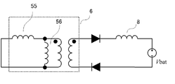
- the main circuit has a transformer 6 having at least two windings.
- the side of the main circuit connected to the AC power source 1 is the primary side and the side connected to the DC load 10 is 2 It will be described as the next side.
- a rectifier circuit (first rectifier circuit) 200 that rectifies AC power
- a reactor 3 that operates as a current limiting circuit
- DC power rectified by the rectifier circuit 200 is supplied to AC power having a desired voltage.
- An inverter circuit 400 is provided that converts the signal into the transformer 6 and outputs it to the transformer 6.
- a rectifier circuit (second rectifier circuit) 700 that rectifies AC power output from the transformer 6 into DC power, and a smoothing reactor that smoothes DC power output from the rectifier circuit 700 are provided. 8 and a smoothing capacitor 9 are provided.
- the rectifier circuit 200 which is the first rectifier circuit is connected to the AC power source 1 and rectifies the input from the AC power source 1 to convert it into DC power.
- the rectifier circuit 200 is a full bridge circuit composed of four diode elements 201 to 204, and the DC terminal of the rectifier circuit 200 is connected to the inverter circuit 400 via the reactor 3.
- the positive terminal is referred to as a positive DC terminal
- the negative terminal is referred to as a negative DC terminal.
- the rectifier circuit 200 is not limited to the above-described configuration, and any circuit that rectifies AC power into DC power may be used.
- a part or all of the diode elements may be replaced with switching elements. You may make it comprise using active elements, such as.
- the reactor 3 is a current limiting reactor having one end connected to the positive side DC terminal of the rectifier circuit 200 and the other end connected to the inverter circuit 400.
- the connection point between the reactor 3 and the inverter circuit 400 is also connected to the primary side terminal of the transformer 6.
- the reactor 3 may be connected to the negative DC terminal of the rectifier circuit 200 or may be connected to each of the two DC terminals of the rectifier circuit 200.
- the inverter circuit 400 is a full-bridge inverter circuit including four semiconductor switching elements 401a to 404a, and each semiconductor switching element performs a switching operation based on a gate signal from the control circuit 11. Further, diodes 401b to 404b are connected in antiparallel to the semiconductor switching elements 401a to 404a, respectively, and capacitors 401c to 404c are connected in parallel to each other, so that semiconductor elements such as MOSFETs can be used.
- the semiconductor switching element 401a (first switching element) and the semiconductor switching element 402a (second switching element), the semiconductor switching element 403a (third switching element) and the semiconductor switching element 404a (fourth switching element) are connected in series.
- the semiconductor switching element 401a and the semiconductor switching element 402a connected in series are referred to as a first leg
- the semiconductor switching element 403a and the semiconductor switching element 404a connected in series are referred to as a second leg.
- the semiconductor switching element 401a has a diagonal relationship with the semiconductor switching element 404a
- the semiconductor switching element 402a has a diagonal relationship with the semiconductor switching element 403a.
- a connection point (first AC terminal) between the semiconductor switching element 401a and the semiconductor switching element 402a is connected to the positive DC terminal of the rectifier circuit 200 through the reactor 3, and is connected to the primary terminal of the transformer 6. Is also connected.
- the inverter circuit 400 includes a DC capacitor 5, and the DC capacitor 5, the first leg, and the second leg are connected in parallel between the DC buses (between the PN buses).
- the negative side bus of the inverter circuit 400 is connected to the negative side DC terminal of the rectifier circuit 200.
- the transformer 6 is an insulating transformer composed of two windings (a primary winding and a secondary winding). One end of the primary winding is a first AC end of the inverter circuit 400 and the other end is a semiconductor switching element. 403a and the semiconductor switching element 404a are connected to a second AC terminal that is a connection point.
- the leakage inductance of the transformer 6 is used as a resonance element, but an external reactor may be used.
- the rectifier circuit 700 which is the second rectifier circuit, is a full bridge circuit composed of four diode elements in the same manner as the rectifier circuit 200.
- the AC terminal of the rectifier circuit 700 is connected to the secondary-side output terminal of the transformer 6, and the AC power output from the transformer 6 is rectified and output from the DC terminal of the rectifier circuit 700.
- the rectifier circuit 700 is a full bridge diode rectification method, but may be any circuit as long as it is a circuit that rectifies AC power output from the transformer 6.
- some or all of the diode elements may be configured using active elements such as semiconductor switching elements.
- the DC terminal on the positive side of the rectifier circuit 700 is connected to the smoothing reactor 8, and the smoothing capacitor 9 is connected to the subsequent stage of the smoothing reactor 8 and the DC terminal on the negative side of the rectifier circuit 700.
- a DC load 10 is connected to the smoothing capacitor 9, and DC power output from the rectifier circuit 700 is supplied to the DC load.
- the DC load 10 is, for example, a storage battery (battery). In addition, it may be a DC load that requires insulation from other AC inputs, and may be constituted by, for example, an electric double layer capacitor.
- a current detector that detects the current (i ac ) that is output from the rectifier circuit 200 and flows through the reactor 3, and a voltage detector that detects the DC voltage (V dc ) of the DC capacitor 5 1 voltage detector), and a voltage detector (second voltage detector) for detecting the voltage (V bat ) of the smoothing capacitor 9 is provided.
- a voltage detector that detects a power supply voltage (V ac ) of the AC power supply 1 and a current detector that detects a current (i bat ) input to the DC load 10 are provided. Information on these voltage value and current value is input to the control circuit 11.
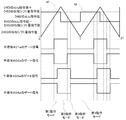
- FIG. 2 is a diagram illustrating a gate waveform for explaining the operation of the semiconductor switching elements 401a to 404a, a current flowing through the reactor 3, and a state of charging / discharging of the DC capacitor 5.
- 3 to 6 are diagrams showing current paths in the power conversion device in the four operation modes defined in FIG.
- the driving period of the semiconductor switching elements 401a, 402a, 403a, and 404a is T
- the switching time of the semiconductor switching elements 401a and 402a that perform current control is t2.
- the OFF timing of the semiconductor switching element 404a is t1
- the OFF timing of the semiconductor switching element 403a is t3.
- the operation mode has four periods of 0 to t1 (first operation mode), t1 to t2 (second operation mode), t2 to t3 (third operation mode), and t3 to T (fourth operation mode).
- FIG. 3 to FIG. 6 show current paths for each of the four operation modes.
- the semiconductor switching elements 401a and 404a are turned on, and the semiconductor switching elements 402a and 403a are turned off.
- the current i ac input from the AC power source 1 and rectified by the rectifier circuit flows through the reactor 3, the transformer 6, and the semiconductor switching element 404a and returns to the input side.
- a current flows from the DC capacitor 5 to the transformer 6 via the semiconductor switching element 401a, and the current returns from the transformer 6 to the DC capacitor 5 via the semiconductor switching element 404a.
- the potential at the subsequent stage of the reactor 3 is fixed to V dc when the semiconductor switching element 401a is turned on.
- the current i ac decreases when the DC voltage V dc of the DC capacitor 5 is controlled to be higher than the peak voltage Vp of the voltage V ac of the AC power supply 1.
- V dc decreases since the DC capacitor 5 discharges current.
- the semiconductor switching elements 401a and 403a are turned on, and the semiconductor switching elements 402a and 404a are turned off.
- the current i ac flows through the reactor 3, the transformer 6, the diode element 403 b, and the DC capacitor 5, and the current returns to the input side. Further, part of the current flowing through the diode element 403b flows through the semiconductor switching element 401a and circulates to the transformer 6.
- the potential at the subsequent stage of the reactor 3 is fixed to V dc when the semiconductor switching element 401 a is turned on, and the voltage V dc of the DC capacitor 5 is higher than the peak voltage Vp of the voltage V ac of the AC power supply 1.
- the current i ac decreases.
- V dc increases.
- the potential difference generated at both ends of the transformer 6 is small, the output amount of power to the secondary side is small and is not considered here.
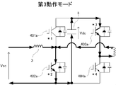
- the operation of the power conversion apparatus in the third operation mode that is, the period from t2 to t3 shown in FIG. 2 will be described.
- the semiconductor switching elements 402a and 403a are turned on, and the semiconductor switching elements 401a and 404a are turned off.
- the current i ac flows back from the reactor 3 to the input side via the semiconductor switching element 402a. Further, a current flows from the DC capacitor 5 to the DC capacitor 5 through the semiconductor switching element 403a, the transformer 6, and the semiconductor switching element 402a.
- the potential at the subsequent stage of the reactor 3 is fixed to 0 when the semiconductor switching element 402a is turned on, and the current i ac increases.
- V dc decreases.
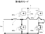
- the fourth operation mode the semiconductor switching elements 402a and 404a are turned on, and the semiconductor switching elements 401a and 403a are turned off.
- the current i ac flows back from the reactor 3 to the input side via the semiconductor switching element 402a. Further, current circulates through the semiconductor switching element 402a, the diode 404b, and the transformer 6.
- the potential at the subsequent stage of the reactor 3 is fixed to 0 when the semiconductor switching element 402a is turned on, and the current i ac increases.
- V dc is constant.
- a current is input to the transformer 6 to supply power to the secondary side, and the polarity of the current is changed between the first operation mode and the third operation mode. It will be reversed.
- an alternating current is input to the transformer 6.
- the AC power input to the primary side of the transformer 6 is transformed according to the ratio of the number of windings and output to the secondary side.
- the AC power is converted into DC power by the rectifier circuit 700, the DC power is smoothed by the smoothing reactor 8 and the smoothing capacitor 9, and the smoothed DC power is supplied to the DC load 10. That is, DC power can be supplied to the DC load 10 during the period of the first operation mode and the third operation mode.
- the first leg on-period that is, the first and second operation modes that are the on-period of the semiconductor switching element 401a, and the on-period of the semiconductor switching element 402a.
- the duty ratio with the third and fourth operation modes is controlled. That is, by controlling the time t2 in FIG. 2, it is possible to control the ratio of increase and decrease of current i ac flowing through the reactor 3, it is possible to control the current i ac flowing through the reactor 3.
- the phase shift amount between the ON period of the first leg and the ON period of the second leg that is, the phase of the driving signal of the semiconductor switching element 403a with respect to the semiconductor switching element 401a and the driving signal of the semiconductor switching element 404a with respect to the semiconductor switching element 402a is shifted.
- the amount (phase shift amount) to be performed the charge amount and discharge amount of the DC capacitor 5 can be adjusted, and the voltage V dc of the DC capacitor 5 can be controlled to be constant.
- the power difference between the AC power captured by the current control and the power supplied to the DC load 10 is adjusted to control the voltage V dc of the DC capacitor 5 to be constant.
- the time t1 and the time t3 in FIG. 2 are controlled.
- the period from 0 to t1 is equal to the period from t2 to t3.
- t2 is a timing determined by current control
- the time ratio (duty ratio) D 401 of the on-time 0 to t2 per switching period T in the semiconductor switching element 401a is expressed by Equation (1)
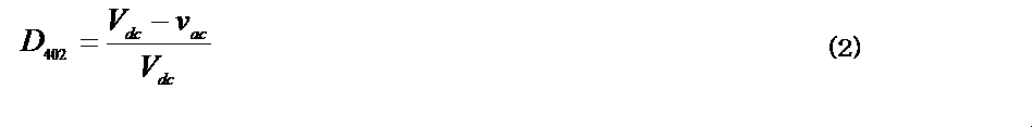
- the time ratio (duty ratio) D 402 of the on-times t2 to T per switching period T in the semiconductor switching element 402a is expressed by Equation (2).
- v ac is the voltage of the AC power supply 1
- V dc is the voltage of the DC capacitor 5.
- the phase shift amount of the second leg is set to zero.
- this phase shift amount is set to 0, so that the rising edge of the semiconductor switching element 403a in the on state is synchronized with the rising edge of the semiconductor switching element 401a.
- the rising edge of the semiconductor switching element 404a is synchronized with the rising edge of the semiconductor switching element 402a. That is, the ON period (gate pulse width) and phase of the third switching element are made equal to those of the first switching element, and the ON period (gate pulse width) and phase of the fourth switching element are made equivalent to those of the second switching element. In this case, only the second and fourth operation modes are operated, and the period of the first and third operation modes is zero.
- the control circuit 11 controls the phase shift amount from this initial state. As a result, power supply can be started gradually in the initial state.
- the rise of the semiconductor switching element 404a in the on state may be synchronized with the rise of the semiconductor switching element 401a in the on state.
- the rising edge of the semiconductor switching element 403a is synchronized with the rising edge of the semiconductor switching element 402a. That is, the ON period (gate pulse width) and phase of the fourth switching element are made equal to those of the first switching element, and the ON period (gate pulse width) and phase of the third switching element are made equal to those of the second switching element. In this case, only the first and third operation modes are operated, and the period of the second and fourth operation modes is zero.
- the control circuit 11 controls the phase shift amount from this initial state. As a result, power supply can be started sharply from the initial state.
- the phase shift amount does not necessarily have to be 0, and a phase shift amount that is determined in advance according to a request in the initial state may be set as the initial state.
- the overlapping period of the semiconductor switching elements 401a and 404a (first operation mode period) is equal to the overlapping period of the semiconductor switching elements 402a and 403a (third operation mode period). Control to be. That is, the periods from 0 to t1 and t2 to t3 in FIG. 2 are equal. Note that the period of the first operation mode and the period of the third operation mode are not necessarily the same.
- the phase shift amount of the second leg corresponds to the length of the period of the first operation mode (t0 to t1) in FIG. 2, and here, it is expressed as a time ratio to match D 401 and D 402. To do.
- the phase shift amount D 403 of the second leg is expressed as Equation (3).
- N1 the number of turns on the primary side of the transformer 6, that is, the AC power supply side
- N2 the number of turns on the secondary side, that is, the DC load side
- V bat is the voltage of the smoothing capacitor 9.
- the semiconductor switching element 403a and the semiconductor switching element 404a are operated with the same phase shift amount in accordance with the phase shift amount shown in Equation (3).
- D 403 must always be lower than D 401 and D 402 . That is, it is necessary to satisfy the relationship of 0 ⁇ t1 ⁇ t2 for t1 and the relationship of t2 ⁇ t3 ⁇ T for t3.
- FIG. 7 shows a schematic duty locus diagram of D 401 and D 402 satisfying this relationship.
- the horizontal axis represents the phase of the voltage V ac of the AC power supply 1
- the vertical axis represents the time ratio of the on-time of each semiconductor switching element to the driving cycle.
- the controllable condition for constant control of the DC capacitor voltage V dc is that D limit in the peak phase, that is, D 403 is smaller than D limit_p . This means that Equation (5) becomes a controllable condition.
- the command value D 403 is controlled to be equal to or less than D limit .
- the locus of D 403 becomes as in FIG. 8, D 403 is greater than D limit, D 403 as D limit, D 403 is the D 403 calculated in Equation (3) If D limit smaller than . In this case, D 403 can always fall below D limit regardless of the phase, and satisfies the controllable condition.
- phase shift amount D 403 of the semiconductor switching element 403a and the semiconductor switching element 404a is a less restricted D limit by D 401 and D 402 determined by current control by the semiconductor switching element 401 a and the semiconductor switching element 402a , V dc constant control is established, and high power factor control and output power control can be realized by one full bridge inverter circuit.
- the DC capacitor 5 Since the DC capacitor 5 is charged and discharged in the drive cycle T of the inverter circuit 400, a voltage ripple based on the drive cycle is generated.
- the voltage ripple is defined by the voltage ripple during the charging period in the second operation mode.
- a voltage ripple having a frequency twice that of the AC frequency is generated in the DC section, but in the power converter shown in the present embodiment, a voltage ripple having a frequency that is twice this frequency is generated. Therefore, the capacity of the DC capacitor 5 can be greatly suppressed, and the DC capacitor 5 can be reduced in size.
- the voltage and current of the AC power source having a power factor of 1 are expressed as in equations (6) and (7). Further, the power P ac of the AC power supply 1 is expressed as shown in Equation (8).
- all Pac expressed by Equation (8) is transmitted to DC load 10. Assuming that the DC load 10 is controlled to a constant voltage V bat , the current I bat supplied to the DC load is defined by (9). Therefore, the current flowing into the DC load 10 has a pulsating component having an AC frequency twice as large.
- FIG. 9 is a control block diagram illustrating generation of a duty command value used in output control of the semiconductor switching element 401a and the semiconductor switching element 402a in the control circuit 11.
- the control circuit 11 calculates a duty command value for controlling the current iac so that the amount of current from the AC power source 1 and the power factor from the AC power source 1 are approximately 1.
- a current difference 20 between a sinusoidal predetermined current command (target sine wave current) i ac * synchronized with the power supply voltage V ac and a current i ac detected by the current detector is calculated.
- the output 21 is calculated by PI control using the calculated current difference 20 as a feedback amount.
- the duty command value 22 of the semiconductor switching element 402a is obtained by dividing the output 21 by the voltage Vdc of the DC capacitor 5 detected by the voltage detector.
- the feed-forward term 23 is a value represented by Expression (2), and is determined for each drive cycle according to the phase of the AC power supply 1.
- the duty command value 24 obtained by adding the feedforward term 23 is set as the duty command value of the semiconductor switching element 402a.
- the duty command value 25 obtained by subtracting the duty command value 24 of the semiconductor switching element 402a from 1 is set as the duty command value of the semiconductor switching element 401a.
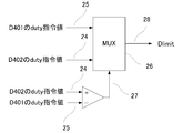
- FIG. 10 is a calculation block diagram of D limit calculated based on the duty command value 24 of the semiconductor switching element 402a and the duty command value 25 of the semiconductor switching element 401a.
- duty selection unit (MUX) 26 in accordance with the magnitude relation of the duty command value 25 of the duty command value 24 and D 401 of D 402, selects a duty command value 24 or the duty command value 25 as D limit. That is, when the duty command value 25 is larger than the duty command value 24, L is output as the comparison signal 27, and the duty command value 24 is selected as the D limit 28 by the duty selector 26. On the other hand, when the duty command value 24 is larger than the duty command value 25, H is output as the comparison signal 27, and the duty command value 25 is selected as the D limit 28 by the duty selector 26.
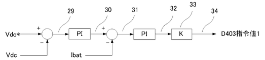
- FIG. 11 is a control block diagram illustrating generation of a D 403 command value in the constant control of the voltage V dc of the DC capacitor 5 by the semiconductor switching element 403a and the semiconductor switching element 404a.
- the output power from the semiconductor switching element 403a and the semiconductor switching element 404a is adjusted to calculate a D 403 command value for controlling the voltage V dc of the DC capacitor 5 to be constant.
- a difference 29 between a predetermined DC voltage command value V dc * of the DC capacitor 5 and the voltage V dc detected by the voltage detector is calculated.
- the DC voltage command value V dc * is set to a voltage value higher than the peak voltage of the AC voltage input from the AC power supply.
- a calculation result obtained by PI control is set as an output current command value 30 to the DC load 10.
- a calculation result 32 obtained by PI control using the difference value 31 between the output current command value 30 and the detected DC current value I bat as a feedback amount is input to the gain adjuster 33 to generate a D 403 command value 34.
- the D 403 command value 34 and D limit 28 are input to the selector (MUX) 35.
- the selector 35 selects the D 403 command value 34 and D limit 28 in accordance with the magnitude comparison calculation result 36 of the D 403 command value 34 and D limit 28.
- the D 403 command value 34 is set as the phase shift amount command value 37 of D 403 .
- D 403 command value 34 is greater than D limit 28, the D limit 28 and the phase shift amount command value 37 of the D 403.
- the phase shift amount command value 37 of D 403 of the semiconductor switching element 403a and the semiconductor switching element 404a can always be equal to or less than D limit 28, and the controllable condition of V dc control can be satisfied.
- the semiconductor switching element 401 a gate signal generated from duty command value 25 of D 401, the gate signal of the semiconductor switching elements 402a to generate the duty command value 24 of D 402, the phase shift amount command value 37 D 403
- a process of generating the gate signals of the semiconductor switching element 403a and the semiconductor switching element 404a to be generated will be described.
- these gate signals are generated using a sawtooth wave as a carrier wave is shown.
- FIG. 13 shows a sawtooth wave 38 as a carrier wave, a duty command value 25 of D 401 , a duty command value 24 of D 402 , a phase shift amount command value 37 of D 403 , and gates of semiconductor switching elements 401a to 404a. Signal relationships are shown.
- FIG. 14 shows a calculation block diagram for generating gate signals of the semiconductor switching element 401a and the semiconductor switching element 402a
- FIG. 15 shows a calculation block diagram for generating gate signals of the semiconductor switching element 403a and the semiconductor switching element 404a.
- the sawtooth wave having the same value and the same phase is used for the four elements from the semiconductor switching elements 401a to 404a.
- the duty command value 24 of D 402 and the sawtooth wave 38 are input to the gate signal generator 39.
- the semiconductor switching element to turn on the semiconductor switching element 402a The gate signal 40 of 402a is generated.
- the gate signal of the semiconductor switching elements 401a to turn on the semiconductor switching element 401a 41 Is generated.
- the semiconductor switching element 401a and the semiconductor switching element 402a on the basis of the semiconductor switching element 401a and the semiconductor switching element 402a is the duty command value 25 of the duty command value 24, D 402 of D 401, which is calculated by the high power factor control Generate a gate signal.
- the phase shift amount command value 37 and the sawtooth wave 38 of D 403 are input to the gate signal generator 42.
- the gate signal generator 44 includes a phase shift amount signal 43 which took the sum of the duty command value 24 of the phase shift amount command value 37 and D 402 of D 403, inputs a sawtooth 38.
- a signal obtained by ANDing the comparison signal of the phase shift amount signal 43 and the sawtooth wave 38 and the comparison signal of the sawtooth wave 38 and the phase shift amount command value 37 of D 403 is defined as a gate signal 45 of the semiconductor switching element 404a.
- a signal obtained by negating the gate signal 45 is defined as a gate signal 46 of the semiconductor switching element 403a.
- the gate signal to the semiconductor switching elements 401a to 404a can be generated.
- FIGS. 9 to 12 and FIG. 14 may be configured in hardware using an arithmetic circuit.
- a memory for storing a program and a processor for processing the program May be configured as software.
- a dead time may be provided.
- a dead time may be provided in the semiconductor switching element 403a and the semiconductor switching element 404a.
- one terminal of the reactor 3 is connected to the P side of the DC output terminal of the rectifier circuit 200, and the other terminal of the reactor 3 is the first AC that is a connection point between the semiconductor switching element 401a and the semiconductor switching element 402a.
- the high power factor control is performed by the semiconductor switching elements 401a and 402a connected to the ends, but the other terminals of the reactor 3 are connected to the connection points of the semiconductor switching elements 403a and 404a and the semiconductor switching elements 403a and 404a are used. High power factor control may be performed.
- a gate signal input to the semiconductor switching element 401a may be input to the semiconductor switching element 403a
- a gate signal input to the semiconductor switching element 402a may be input to the semiconductor switching element 404a.
- the semiconductor switching element High power factor control is performed at 401a and 402a, and output power control is performed at the semiconductor switching element 403a and the semiconductor switching element 404a.
- the on-duty of the semiconductor switching element 401a and the semiconductor switching element 402a is controlled to adjust the input current from the AC power supply 1 to a predetermined current value
- the power factor can be controlled to be about 1.
- the DC voltage of the DC capacitor 5 is controlled to be constant by changing the phase shift amount of the semiconductor switching element 403a and the semiconductor switching element 404a so that the DC voltage Vdc of the DC capacitor 5 follows the target voltage.
- the output power to can be controlled.
- the on-state overlapping period of the semiconductor switching element 401a and the semiconductor switching element 404a and the on-state overlapping period of the semiconductor switching element 402a and the semiconductor switching element 404a are made equal to suppress the bias magnetism of the transformer 6, thereby improving reliability. High control can be realized.
- Embodiment 2 FIG.
- the sawtooth wave is used as the on-period control carrier signal in the generation of the gate signals of the semiconductor switching elements 401a to 404a.
- a triangular wave is used as the on-period control carrier signal. Show the case.
- the circuit configuration and control method of the power conversion device in the present embodiment are the same as those shown in the first embodiment, and a description thereof will be omitted.
- the calculation results of the duty command value 25 of D 401 , the duty command value 24 of D 402 , and the phase shift amount command value 37 of D 403 are calculated by the same method as in the first embodiment. That is, the operation other than the gate signal generation operation of each semiconductor switching element shown in FIGS. 13 to 15 is the same as that shown in the first embodiment.
- the gate signal of the semiconductor switching element 401a generated from the duty command value 25 of D 401 in the present embodiment, the gate signal of the semiconductor switching element 402a generated from the duty command value 24 of D 402 , and the phase shift amount command value The gate signal generation process of each of the semiconductor switching element 403a and the semiconductor switching element 404a generated from 37 will be described.
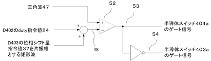
- FIG. 17 shows a carrier wave 47, a duty command value 25 of D 401 , a duty command value 24 of D 402 , a phase shift amount command value 37 of D 403 , and gate signals of the semiconductor switching elements 401a to 404a.
- the figure showing the relationship of is shown.
- the carrier wave 47 is a triangular wave, and the same triangular wave is used to generate the gate signals of the semiconductor switching elements 401a to 404a.
- the phase of the semiconductor switching element 403a is shifted with respect to the semiconductor switching element 401a due to the magnitude relationship between the rectangular wave 48 and the triangular wave 47 whose amplitude is the phase shift amount command value of D 403.
- the phase of the semiconductor switching element 404a is shifted with respect to the semiconductor switching element 402a.
- the value of the square wave is switched between the peak and valley of the triangular wave.
- the semiconductor switching element 401a has the same configuration in the four operation modes defined in the first embodiment.
- the semiconductor switching element 402a performs high power factor control, and the semiconductor switching element 403a and the semiconductor switching element 404a perform output power control.
- two DC signals having the same value as the rectangular wave amplitude may be used, and the signal to be compared in magnitude at the timing of the peaks and valleys of the triangular wave 47 may be switched to form a pseudo rectangular wave.
- Figure 18 shows a block diagram for generating a gate signal of the gate signal and the semiconductor switching element 402a of the semiconductor switching element 401a from the duty command value 24 of the duty command value 25 and D 402 of the D 401.
- the duty command value 24 of D 402 and the triangular wave 47 are input to the gate signal generator 49.
- the gate signal 50 of the semiconductor switching element 402 a is generated so that the duty command value 24 of D 402 is turned on in a period longer than the triangular wave 47.
- the gate signal 51 of the semiconductor switching element 401 a is generated so that the duty command value 24 of D 402 is turned on in a period smaller than the triangular wave 47.
- FIG. 19 is a calculation block diagram showing a method for generating gate signals of the semiconductor switching elements 403a and 404a.
- the rectangular wave 48 is generated by adding the duty command value 24 of D 402 and the phase shift amount command value 37 of D 403 to a single amplitude.
- the generated rectangular wave 48 and triangular wave 47 are input to the comparator 52.
- a calculation result 53 obtained by comparing the rectangular wave 48 and the triangular wave 47 is used as a gate signal of the semiconductor switching element 404a.
- the signal 54 obtained by negating the calculation result 53 is used as the gate signal of the semiconductor switching element 403a.
- the gate signals of the semiconductor switching elements 401a to 404a can be generated.
- Embodiment 3 In the power conversion devices shown in the first and second embodiments, in the return period (second operation mode or fourth operation mode) in which semiconductor switching elements 401a and 403a or semiconductor switching elements 402a and 404a are turned on, Since the potential difference generated at both ends is small, the output amount to the secondary side is small and has not been considered. However, in the present embodiment, the potential difference generated at both ends of the transformer 6 is taken into consideration, and the power that enables more stable operation. The conversion device will be described. In addition, the structure of the power converter device shown in this Embodiment is the same as that of the case shown in FIG. 1, and abbreviate
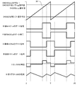
- FIG. 20 shows a sawtooth wave 38 that is a carrier wave, a duty command value 25 of D 401, and a duty of D 402 , in consideration of the voltage across the minute transformer 6 generated in the second operation mode and the fourth operation mode.
- the relationship between the command value 24, the phase shift amount command value 37 of D 403 , the gate signals of the semiconductor switching elements 401a to 404a, the voltage of the transformer 6, and the current of the smoothing reactor 8 is shown.
- a minute voltage across the transformer 6 is also generated during the return period.
- FIG. 21 shows a simple equivalent circuit during the reflux period in which the semiconductor switching elements 401a and 403a or the semiconductor switching elements 402a and 404a are turned on.
- the both-ends voltage V tr_p of the transformer 6 is expressed as the following formula (10).
- the forward voltage of the diodes 701 to 704 is defined as V f
- the leakage inductance of the transformer 6 is defined as L k
- the inductance value of the smoothing reactor 8 is defined as Lf.
- the leakage inductance 55 and the excitation inductance 56 of the transformer 6 may be external reactors.
- the transformer 6 by correcting the power transmission period (first operation mode and third operation mode) and the return period (second operation mode and fourth operation mode), the transformer 6 The voltage / time product deviation and the current integrated value deviation of the current in the smoothing reactor 8 are reduced. The details will be described below.
- the time ratio (duty ratio) D 401 of the semiconductor switching element 401a, the time ratio (duty ratio) D 402 of the semiconductor switching element 402a, and the phase shift amount D 403 of the second leg are set as in the first embodiment.
- the calculation is performed in the same manner as in the second embodiment. In the power conversion device described in this embodiment, correction is performed on these calculated values.
- FIG. 22 shows a schematic duty locus diagram when the phase shift amount D 403 of the second leg composed of the semiconductor switching element 403a and the semiconductor switching element 404a is corrected.
- the phase shift amount of the second leg is corrected as shown by the locus indicated by D 403 -2.
- D 403 -2 the locus indicated by D 403 -2.
- by correcting the phase shift amount of the second leg by correcting the phase shift amount of the second leg, the on-time and the phase shift amount of the semiconductor switching element 403a and the semiconductor switching element 404a change. Accordingly, it is possible to suppress the voltage / time product deviation of the transformer 6 and the current integrated value deviation of the current in the smoothing reactor 8.
- a correction period in the power transmission period at this time is defined as ⁇ T.
- ⁇ T defines that the polarity of increasing the power transmission period composed of the semiconductor switching element 402a and the semiconductor switching element 403a is positive.
- both ends are increased or decreased by ⁇ T / 2 with reference to the center of the gate signal phase in the semiconductor switching element 403a and the semiconductor switching element 404a. Instead of reducing both ends by ⁇ T / 2, either pulse end may be increased or decreased by ⁇ T.
- the duty ratio (on time) of the first leg composed of the semiconductor switching element 401a and the semiconductor switching element 402a may be corrected.
- the phase shift amount D 403 is the first operating sub-mode a smaller period than D limit, D 403 is defined as a second operating sub-mode period is D limit or more.
- D 403 is defined as a second operating sub-mode period is D limit or more.
- the ON timing of the semiconductor switching element 402a when considering the correction period ⁇ T1 is t02
- the OFF timing of the semiconductor switching element 403a is t12.
- the ON timing of the semiconductor switching element 401a is t22
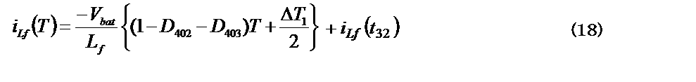
- the OFF timing of the semiconductor switching element 404a is t32. In this case, it can be classified into four operation modes of t02 to t12, t12 to t22, t22 to t32, and t32 to T.
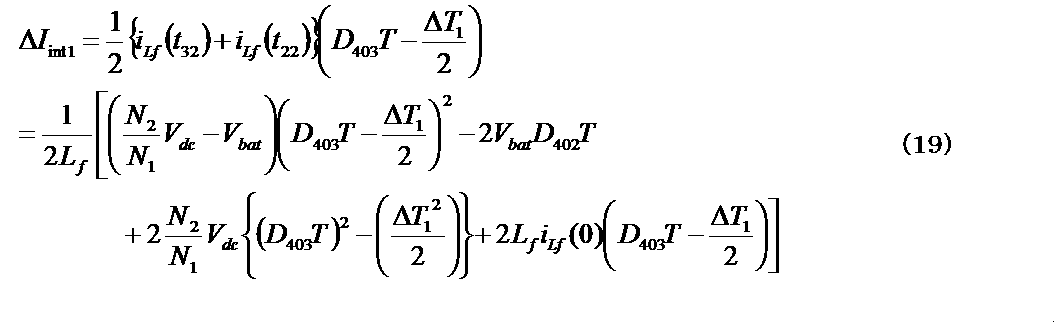
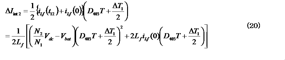
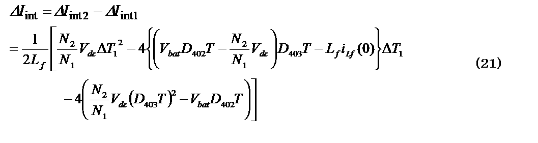
- ⁇ I int1 represents the time integral value of the smoothing reactor 8 current when the semiconductor switching elements 401a and 404a are in the ON state
- ⁇ I int2 represents the time integral value of the smoothing reactor 8 current when the semiconductor switching elements 402a and 403a are in the ON state.
- the above four operation mode periods can be expressed as the following formulas (11) to (14), respectively. Note that the initial time t02 is set to zero.
- the initial current i Lf of the smoothing reactor 8 in each operation mode can be expressed as follows.
- ⁇ 1 in the formula (22) is defined as follows.
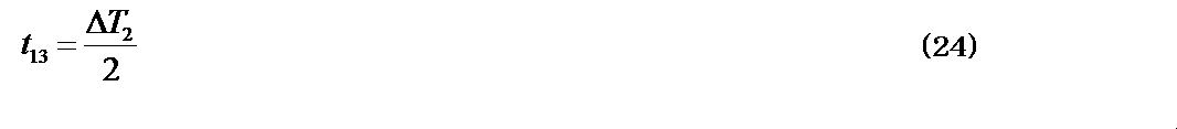
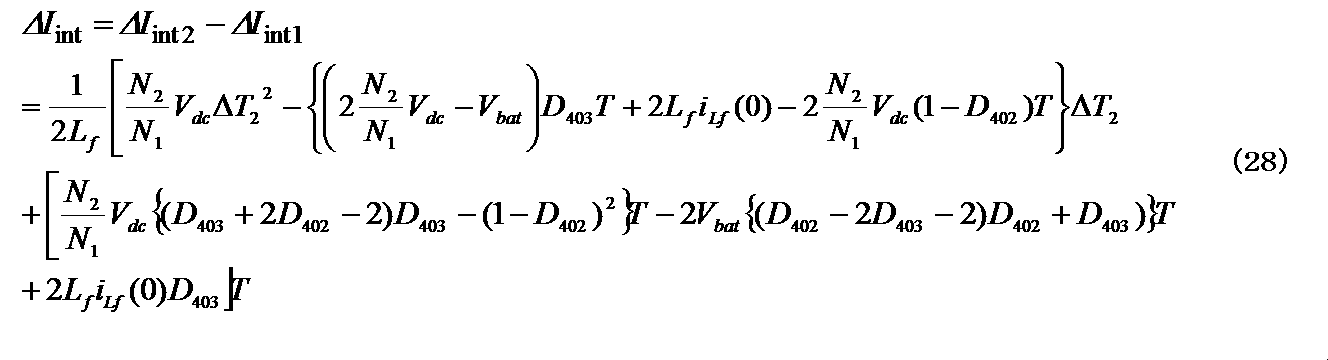
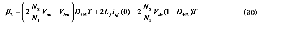
- the ON timing of the semiconductor switching element 402a when the correction period ⁇ T2 is taken into consideration is t03, and the OFF timing of the semiconductor switching element 403a is t13.
- the ON timing of the semiconductor switching element 401a is t23, and the OFF timing of the semiconductor switching element 404a is t33. In this case, it can be classified into four operation modes of t03 to t13, t13 to t23, t23 to t33, and t33 to T.
- the initial time t03 is set to 0.
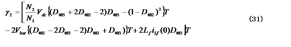
- the correction periods of the mathematical expressions (22) and (29) are respectively the DC capacitor 5 voltage (V dc ), the smoothing capacitor 9 voltage (V bat ) detection value, and the smoothing reactor 8 current value ( i Lf ), the duty ratio D 401 of the semiconductor switching element 401a, the duty ratio D 402 of the semiconductor switching element 402a, and the phase shift amount D 403 of the second leg can be calculated.
- the voltage value (V dc ) of the DC capacitor 5 and the voltage value (V bat ) of the smoothing capacitor 9 do not necessarily have to be detected values, and may be target voltages of the respective voltage values or may be calculated values. Good.
- the current value (i Lf ) of the smoothing reactor 8 is not necessarily a calculated value, and a detection value detected by a current detector may be used.
- the duty ratio (ON time) of the first leg including the semiconductor switching element 401a and the semiconductor switching element 402a may be corrected.
- the duty ratios of the semiconductor switching element 401a and the semiconductor switching element 402a are corrected using correction values similar to those in Expression (22) and Expression (29). That is, the voltage value of the DC capacitor, the voltage value of the smoothing capacitor, the current value of the smoothing reactor, the calculated value of the duty ratio of the first switching element, the duty ratio of the second switching element, The on period of the first leg is corrected based on the calculated value of the phase shift amount of the second leg.
- the upper limit value of the phase shift amount D 403 depends on the duty ratios D 401 and D 402 of the semiconductor switching elements 401a and 402a, so that D 401 and D 402 are When corrected, the upper limit value of the phase shift amount D 403 is also corrected accordingly.
- the generation process of the gate signal of the semiconductor switching element 401a generated from the duty command value 25 of D 401 and the gate signal of the semiconductor switching element 402a generated from the duty command value 24 of D 402 in this embodiment are as follows. This is the same method as in Embodiment 1 and Embodiment 2, and will not be described.
- the carrier wave is a sawtooth wave as in the first embodiment
- the gate signal generation process of each of the semiconductor switching element 403a and the semiconductor switching element 404a generated from the phase shift amount command value 37 and the correction period of the power transmission period is as follows. explain.
- Figure 27 is a formula (22) in equation (29), a correction period ⁇ T1 is calculated by substituting the instantaneous value of the apparatus operating Delta] T2, and the phase shift amount command value 37 and D limit 28 of D 403 3 is a calculation block diagram for generating duty correction values dt of the semiconductor switching element 403a and the semiconductor switching element 404a.
- the correction period ⁇ T1 (57) and the correction period ⁇ T2 (58) are input to the selector (MUX) 59.
- the selector 59 selects the correction period ⁇ T1 (57) and the correction period ⁇ T2 (58) according to the magnitude comparison calculation result 60 of the D 403 phase shift amount command value 37 and the D limit 28.
- phase shift amount command value 37 of D 403 is smaller than D limit 28, the correction period ⁇ T1 (57) is set as the correction value 61.
- the correction period ⁇ T2 (58) is set as the correction value 61.
- a duty correction value dt63 is output from the product of the switching frequency 62 and the correction value 61 of the semiconductor switching elements 401a to 404a.
- the addition value 64 of the duty correction value dt 63 and the phase shift amount command value 37 of D 403 and the sawtooth wave 38 are input to the gate signal generator 65.
- a difference value 67 between the phase shift amount signal 66 and the duty correction value dt 63 and the sawtooth wave 38 are input to the gate signal generator 68.
- a signal obtained by ANDing the comparison signal 69 between the added value 64 and the sawtooth wave 38 and the comparison signal 70 between the sawtooth wave 38 and the difference value 67 is defined as a gate signal 71 of the semiconductor switching element 404a.
- a signal obtained by negating the gate signal 71 is defined as a gate signal 72 of the semiconductor switching element 403a.
- the gate signal to the semiconductor switching elements 403a and 404a can be generated.
- the carrier wave may be a triangular wave as shown in the second embodiment.
- the configuration and control described above are performed in the first and second embodiments while realizing a stable operation that suppresses the demagnetization phenomenon of the transformer 6.
- high power factor control and output power control can be realized simultaneously with one stage of a full bridge inverter circuit.
Landscapes
- Engineering & Computer Science (AREA)
- Power Engineering (AREA)
- Dc-Dc Converters (AREA)
- Inverter Devices (AREA)
Abstract
Description
本発明の実施の形態1に係る電力変換装置の構成を、図面を用いて説明する。図1は、本発明の実施の形態1に係る電力変換装置の構成図である。図1に示す電力変換装置は、交流電源1および直流負荷10と接続されており、交流電源1から入力される交流電力を直流電力に変換し、直流負荷10に出力する。


実施の形態1では、半導体スイッチング素子401a~404aのゲート信号の作成において、オン期間制御用キャリア信号に鋸波を用いていたが、実施の形態2ではオン期間制御用キャリア信号に三角波を用いた場合について示す。
実施の形態1および2に示す電力変換装置では、半導体スイッチング素子401aと403a、もしくは半導体スイッチング素子402aと404aがON状態となる還流期間(第2動作モードまたは第4動作モード)において、トランス6の両端に生じる電位差が小さいため2次側への出力量は小さく、考慮しないものとして説明したが、本実施の形態ではトランス6の両端に生じる電位差を考慮し、より安定した動作を可能とする電力変換装置について説明する。なお、本実施の形態に示す電力変換装置の構成は、図1に示す場合と同様であり、説明を省略する。


Claims (14)
- 交流電源より入力された交流電力を整流する第1整流回路と、
直列接続された第1スイッチング素子および第2スイッチング素子を有し、前記第1スイッチング素子および前記第2スイッチング素子との接続点である第1交流端に前記第1整流回路の正極側直流端子が接続された第1レグ、ダイオードが逆並列にそれぞれ接続された第3スイッチング素子および第4スイッチング素子を有し、前記第3スイッチング素子および前記第4スイッチング素子が直列接続された第2レグ、直流コンデンサ、が互いに並列接続され、負極側直流母線が前記第1整流回路の負極側直流端子に接続されたインバータ回路と、
1次巻線および2次巻線を有し、前記1次巻線の一端に前記インバータ回路の前記第1交流端、他端に前記第3スイッチング素子および第4スイッチング素子の接続点である第2交流端が接続されたトランスと、
一端が前記トランスの前記2次巻線に接続され、他端が平滑コンデンサを介して直流負荷に接続され、トランスより入力される交流電力を整流して前記直流負荷に出力する第2整流回路と、
前記インバータ回路の動作を制御する制御回路と、を備え、
前記制御回路は、前記第1レグのオン期間を制御することより前記第1整流回路より出力される電流を制御し、
前記第2レグのオン期間、および、前記第1レグのオン期間と前記第2レグのオン期間との位相シフト量を制御することより前記直流コンデンサの電圧を一定となるように制御すること、
を特徴とする電力変換装置。 - 前記制御回路は、
前記第1スイッチング素子および前記第4スイッチング素子をオンとする第1動作モードと、
前記第1スイッチング素子および前記第3スイッチング素子をオンとする第2動作モードと、
前記第2スイッチング素子および前記第3スイッチング素子をオンとする第3動作モードと、
前記第2スイッチング素子および前記第4スイッチング素子をオンとする第4動作モードと、を用い、前記第1~第4動作モードの各期間を制御することにより前記インバータ回路を制御すること、
を特徴とする請求項1に記載の電力変換装置。 - 前記制御回路は、前記第1整流回路より出力される電流が予め定められた目標正弦波電流になるように前記第1レグのオン期間を制御し、
前記直流コンデンサの電圧が、前記交流電源より入力される交流電圧のピーク電圧よりも高い目標電圧になるように前記第2レグのオン期間と位相シフト量を制御すること、
を特徴とする請求項1または2のいずれかに記載の電力変換装置。 - 前記制御回路は、前記第2レグの位相シフト量を、前記第1スイッチング素子および前記第2スイッチング素子の2つのデューティ比のうち、より小さい方を上限として制御すること、
を特徴とする請求項3に記載の電力変換装置。 - 前記制御回路は、前記第3スイッチング素子および前記第4スイッチング素子の位相シフトするタイミングを同期させること、
を特徴とする請求項3に記載の電力変換装置。 - 前記制御回路は、前記第1スイッチング素子のオン期間と、対角の関係にある前記第4スイッチング素子のオン期間とが重なり合う期間と、
前記第2スイッチング素子のオン期間と、対角の関係にある前記第3スイッチング素子のオン期間とが重なり合う期間を等しくなるように、前記第1レグおよび第2レグのオン期間と前記第2レグの位相シフト量を制御することを特徴とする請求項3に記載の電力変換装置。 - 前記制御回路は、前記第1スイッチング素子と前記第2スイッチング素子とをオンオフが反転するように制御し、
位相シフト量をゼロとする初期状態で、前記第3スイッチング素子のゲートパルス幅および位相を前記第1スイッチング素子と等しくし、
前記第4スイッチング素子のゲートパルス幅および位相を前記第2スイッチング素子と等しくすること、
を特徴とする請求項3~6のいずれか1項に記載の電力変換装置。 - 前記制御回路は、前記第1スイッチング素子と前記第2スイッチング素子とをオンオフが反転するように制御し、
位相シフト量をゼロとする初期状態で、前記第3スイッチング素子のゲートパルス幅および位相を前記第2スイッチング素子と等しくし、
前記第4スイッチング素子のゲートパルス幅および位相を前記第1スイッチング素子と等しくすること、
を特徴とする請求項3~6のいずれか1項に記載の電力変換装置。 - 前記制御回路は、前記第1レグ、前記第2レグのキャリア波に鋸波を用い、
位相シフト量が増加するにしたがい、前記第3スイッチング素子のオン時間を前記第1スイッチング素子のオン時間と等しくしつつ、
前記第3スイッチング素子のゲートパルスの立ち上がりの位相が、前記第1スイッチング素子のゲートパルスの立ち上がりの位相に対してシフトし、
前記第4スイッチング素子のオン時間を前記第2スイッチング素子のオン時間と等しくしつつ、
前記第4スイッチング素子のゲートパルスの立ち上がりの位相が、前記第2スイッチング素子のゲートパルスの立ち上がりの位相に対してシフトすること、
を特徴とする請求項7に記載の電力変換装置。 - 前記制御回路は、前記第1レグ、前記第2レグのキャリア波に三角波を用い、
位相シフト量が増加するにしたがい、
前記第3スイッチング素子のオン時間を前記第1スイッチング素子のオン時間と等しくしつつ、
前記第3スイッチング素子のゲートパルスの立ち上がりの位相が、前記第1スイッチング素子のゲートパルスの立ち上がりの位相に対してシフトし、
前記第4スイッチング素子のオン時間を前記第2スイッチング素子のオン時間と等しくしつつ、
前記第4スイッチング素子のゲートパルスの立ち上がりの位相が、前記第2スイッチング素子のゲートパルスの立ち上がりの位相に対してシフトすること、
を特徴とする請求項7に記載の電力変換装置。 - 前記制御回路は、前記第1レグ、前記第2レグのキャリア波に鋸波を用い、
位相シフト量が増加するにしたがい、
前記第3スイッチング素子のオン時間を前記第1スイッチング素子のオン時間と等しくしつつ、
前記第3スイッチング素子のゲートパルスの立ち上がりの位相が、前記第2スイッチング素子のゲートパルスの立ち上がりの位相に対してシフトし、
前記第4スイッチング素子のオン時間を前記第2スイッチング素子のオン時間と等しくしつつ、
前記第4スイッチング素子のゲートパルスの立ち上がりの位相が、前記第1スイッチング素子のゲートパルスの立ち上がりの位相に対してシフトすること、
を特徴とする請求項8に記載の電力変換装置。 - 前記制御回路は、前記第1レグ、前記第2レグのキャリア波に三角波を用い、
位相シフト量が増加するにしたがい、
前記第3スイッチング素子のオン時間を前記第1スイッチング素子のオン時間と等しくしつつ、
前記第3スイッチング素子のゲートパルスの立ち上がりの位相が、前記第2スイッチング素子のゲートパルスの立ち上がりの位相に対してシフトし、
前記第4スイッチング素子のオン時間を前記第2スイッチング素子のオン時間と等しくしつつ、
前記第4スイッチング素子のゲートパルスの立ち上がりの位相が、前記第1スイッチング素子のゲートパルスの立ち上がりの位相に対してシフトすること、
を特徴とする請求項8に記載の電力変換装置。 - 前記第2整流回路の直流端子に接続された平滑リアクトルと、
を備え、
前記制御回路は、前記直流コンデンサの電圧値と、前記平滑コンデンサの電圧値と、前記平滑リアクトルの電流値と、前記第1スイッチング素子のデューティ比の演算値と、前記第2スイッチング素子のデューティ比と、前記第2レグの位相シフト量の演算値とに基づいて、前記第2レグのオン期間を制御すること、
を特徴とする請求項6に記載の電力変換装置。 - 前記第2整流回路の直流端子に接続された平滑リアクトルと、
を備え、
前記制御回路は、前記直流コンデンサの電圧値と、前記平滑コンデンサの電圧値と、前記平滑リアクトルの電流値と、前記第1スイッチング素子のデューティ比の演算値と、前記第2スイッチング素子のデューティ比と、前記第2レグの位相シフト量の演算値とに基づいて、前記第1レグのオン期間を制御すること、
を特徴とする請求項6に記載の電力変換装置。
Priority Applications (4)
| Application Number | Priority Date | Filing Date | Title |
|---|---|---|---|
| JP2017524483A JP6218996B1 (ja) | 2016-01-29 | 2017-01-26 | 電力変換装置 |
| US15/769,376 US10454364B2 (en) | 2016-01-29 | 2017-01-26 | Power convertor |
| EP17744326.4A EP3410593B1 (en) | 2016-01-29 | 2017-01-26 | Power converter |
| CN201780005104.3A CN108575106B (zh) | 2016-01-29 | 2017-01-26 | 电力转换装置 |
Applications Claiming Priority (2)
| Application Number | Priority Date | Filing Date | Title |
|---|---|---|---|
| JP2016015524 | 2016-01-29 | ||
| JP2016-015524 | 2016-01-29 |
Publications (1)
| Publication Number | Publication Date |
|---|---|
| WO2017131096A1 true WO2017131096A1 (ja) | 2017-08-03 |
Family
ID=59398581
Family Applications (1)
| Application Number | Title | Priority Date | Filing Date |
|---|---|---|---|
| PCT/JP2017/002759 Ceased WO2017131096A1 (ja) | 2016-01-29 | 2017-01-26 | 電力変換装置 |
Country Status (5)
| Country | Link |
|---|---|
| US (1) | US10454364B2 (ja) |
| EP (1) | EP3410593B1 (ja) |
| JP (1) | JP6218996B1 (ja) |
| CN (1) | CN108575106B (ja) |
| WO (1) | WO2017131096A1 (ja) |
Cited By (2)
| Publication number | Priority date | Publication date | Assignee | Title |
|---|---|---|---|---|
| JP2019033654A (ja) * | 2017-08-10 | 2019-02-28 | 新電元工業株式会社 | 電源回路及び電源回路の制御方法 |
| CN110957800A (zh) * | 2019-11-30 | 2020-04-03 | 杭州优迈科技有限公司 | 电梯供电系统的供电控制方法以及电梯供电系统 |
Families Citing this family (7)
| Publication number | Priority date | Publication date | Assignee | Title |
|---|---|---|---|---|
| SG11202011091QA (en) * | 2018-05-10 | 2020-12-30 | Toshiba Kk | Dc transformation system |
| AU2020214609B2 (en) * | 2019-01-30 | 2022-11-10 | Daikin Industries, Ltd. | Power conversion device |
| DE102019215645A1 (de) * | 2019-10-11 | 2021-04-15 | Robert Bosch Gmbh | Ladegerät und Verfahren zum Betrieb des Ladegerätes |
| JP7130024B2 (ja) * | 2020-11-12 | 2022-09-02 | 三菱電機株式会社 | 電力変換装置 |
| CN112448587B (zh) * | 2020-11-16 | 2022-05-27 | 上海空间电源研究所 | 基于隔离式宽范围高压柔性直流组合变换器的控制电路 |
| TWI765547B (zh) * | 2021-01-28 | 2022-05-21 | 台達電子工業股份有限公司 | 具有磁偏平衡控制之隔離型轉換裝置及其磁偏平衡控制方法 |
| CN118694178A (zh) * | 2023-03-21 | 2024-09-24 | 台达电子企业管理(上海)有限公司 | 直流偏置抑制方法及使用其的高频功率变换电路 |
Citations (8)
| Publication number | Priority date | Publication date | Assignee | Title |
|---|---|---|---|---|
| JP2009131007A (ja) * | 2007-11-21 | 2009-06-11 | Daihen Corp | 電源装置及びアーク加工用電源装置 |
| JP2009207304A (ja) * | 2008-02-28 | 2009-09-10 | Hitachi Ltd | インバータ及び偏磁抑制方法 |
| WO2010137278A1 (ja) * | 2009-05-27 | 2010-12-02 | パナソニック株式会社 | インバータ制御装置およびインバータ制御方法 |
| JP2012249375A (ja) | 2011-05-26 | 2012-12-13 | Hitachi Computer Peripherals Co Ltd | 電源装置 |
| JP2012257399A (ja) * | 2011-06-09 | 2012-12-27 | Toshiba It & Control Systems Corp | 電力変換装置及びその制御装置 |
| JP2013158122A (ja) * | 2012-01-30 | 2013-08-15 | Hitachi Ltd | 電力変換装置、電力変換装置の制御方法、およびハードディスク装置 |
| WO2015174123A1 (ja) * | 2014-05-15 | 2015-11-19 | 三菱電機株式会社 | 電力変換装置 |
| JP2015220792A (ja) * | 2014-05-14 | 2015-12-07 | 株式会社ダイヘン | 電源装置及び溶接用電源装置 |
Family Cites Families (25)
| Publication number | Priority date | Publication date | Assignee | Title |
|---|---|---|---|---|
| US44278A (en) * | 1864-09-20 | Improved mode of connecting cars to trucks | ||
| US8945A (en) * | 1852-05-11 | Gold-beating machinery | ||
| JPH10257767A (ja) * | 1997-03-07 | 1998-09-25 | Hitachi Computer Peripherals Co Ltd | 高力率スイッチングレギュレータ及び該スイッチングレギュレータを含む電源装置 |
| KR19990012879A (ko) * | 1997-07-31 | 1999-02-25 | 이형도 | 전원공급장치의 역률개선회로 |
| JPH11243646A (ja) * | 1998-02-23 | 1999-09-07 | Nippon Electric Ind Co Ltd | 充電器用のコンバータ回路 |
| JP4382665B2 (ja) * | 2002-08-19 | 2009-12-16 | 株式会社MERSTech | パルス電源装置 |
| TWI340528B (en) * | 2007-04-03 | 2011-04-11 | Delta Electronics Inc | Resonant converter system and controlling method thereof having relatively better efficiency |
| US8080973B2 (en) * | 2008-10-22 | 2011-12-20 | General Electric Company | Apparatus for energy transfer using converter and method of manufacturing same |
| EP2357720B1 (en) * | 2008-12-12 | 2017-12-06 | Mitsubishi Electric Corporation | Power conversion device |
| JP5644125B2 (ja) * | 2010-02-03 | 2014-12-24 | 富士電機株式会社 | 直流−直流変換回路の起動方法 |
| US20110273909A1 (en) * | 2010-05-04 | 2011-11-10 | Chicony Power Technology Co., Ltd. | Full-bridge phase-shift converter with auxiliary zero-voltage-switching circuit |
| JP5189620B2 (ja) * | 2010-06-29 | 2013-04-24 | 三菱電機株式会社 | Dc/dc電力変換装置 |
| CN103053104B (zh) * | 2010-07-30 | 2015-04-08 | 三菱电机株式会社 | Dc/dc转换器 |
| US9065341B2 (en) * | 2011-02-04 | 2015-06-23 | Mitsubishi Electric Corporation | DC-DC converter |
| JP5914989B2 (ja) * | 2011-05-30 | 2016-05-11 | サンケン電気株式会社 | スイッチング電源装置 |
| JP5803945B2 (ja) * | 2012-05-10 | 2015-11-04 | 株式会社日本自動車部品総合研究所 | 電力変換装置 |
| JP5538658B2 (ja) * | 2012-05-24 | 2014-07-02 | 三菱電機株式会社 | 電力変換装置 |
| WO2015045485A1 (ja) * | 2013-09-30 | 2015-04-02 | 三菱電機株式会社 | 電力変換装置 |
| US9325235B2 (en) * | 2014-03-17 | 2016-04-26 | Cistel Technology Inc. | Adaptive nonlinear current observer for boost PFC AC/DC converters |
| JP6153491B2 (ja) * | 2014-03-28 | 2017-06-28 | オムロンオートモーティブエレクトロニクス株式会社 | 電力供給装置 |
| JP6001587B2 (ja) * | 2014-03-28 | 2016-10-05 | 株式会社デンソー | 電力変換装置 |
| EP3151361B1 (en) * | 2014-05-30 | 2020-09-23 | Fuji Electric Co., Ltd. | Charger |
| US9929660B2 (en) * | 2014-10-20 | 2018-03-27 | Mitsubishi Electric Corporation | Electric power conversion device |
| EP3220531B1 (en) * | 2014-11-11 | 2024-09-25 | Mitsubishi Electric Corporation | Power conversion device |
| EP3229358B1 (en) * | 2014-12-05 | 2019-03-20 | Panasonic Intellectual Property Management Co., Ltd. | Switching power supply device |
-
2017
- 2017-01-26 US US15/769,376 patent/US10454364B2/en active Active
- 2017-01-26 CN CN201780005104.3A patent/CN108575106B/zh active Active
- 2017-01-26 WO PCT/JP2017/002759 patent/WO2017131096A1/ja not_active Ceased
- 2017-01-26 EP EP17744326.4A patent/EP3410593B1/en active Active
- 2017-01-26 JP JP2017524483A patent/JP6218996B1/ja active Active
Patent Citations (8)
| Publication number | Priority date | Publication date | Assignee | Title |
|---|---|---|---|---|
| JP2009131007A (ja) * | 2007-11-21 | 2009-06-11 | Daihen Corp | 電源装置及びアーク加工用電源装置 |
| JP2009207304A (ja) * | 2008-02-28 | 2009-09-10 | Hitachi Ltd | インバータ及び偏磁抑制方法 |
| WO2010137278A1 (ja) * | 2009-05-27 | 2010-12-02 | パナソニック株式会社 | インバータ制御装置およびインバータ制御方法 |
| JP2012249375A (ja) | 2011-05-26 | 2012-12-13 | Hitachi Computer Peripherals Co Ltd | 電源装置 |
| JP2012257399A (ja) * | 2011-06-09 | 2012-12-27 | Toshiba It & Control Systems Corp | 電力変換装置及びその制御装置 |
| JP2013158122A (ja) * | 2012-01-30 | 2013-08-15 | Hitachi Ltd | 電力変換装置、電力変換装置の制御方法、およびハードディスク装置 |
| JP2015220792A (ja) * | 2014-05-14 | 2015-12-07 | 株式会社ダイヘン | 電源装置及び溶接用電源装置 |
| WO2015174123A1 (ja) * | 2014-05-15 | 2015-11-19 | 三菱電機株式会社 | 電力変換装置 |
Non-Patent Citations (1)
| Title |
|---|
| See also references of EP3410593A4 |
Cited By (2)
| Publication number | Priority date | Publication date | Assignee | Title |
|---|---|---|---|---|
| JP2019033654A (ja) * | 2017-08-10 | 2019-02-28 | 新電元工業株式会社 | 電源回路及び電源回路の制御方法 |
| CN110957800A (zh) * | 2019-11-30 | 2020-04-03 | 杭州优迈科技有限公司 | 电梯供电系统的供电控制方法以及电梯供电系统 |
Also Published As
| Publication number | Publication date |
|---|---|
| EP3410593A1 (en) | 2018-12-05 |
| EP3410593B1 (en) | 2022-05-25 |
| JP6218996B1 (ja) | 2017-10-25 |
| US10454364B2 (en) | 2019-10-22 |
| US20180323700A1 (en) | 2018-11-08 |
| CN108575106B (zh) | 2020-06-23 |
| JPWO2017131096A1 (ja) | 2018-02-01 |
| EP3410593A4 (en) | 2019-01-09 |
| CN108575106A (zh) | 2018-09-25 |
Similar Documents
| Publication | Publication Date | Title |
|---|---|---|
| JP6218996B1 (ja) | 電力変換装置 | |
| US11056979B2 (en) | Power conversion apparatus | |
| JP6569839B1 (ja) | 電力変換装置 | |
| JP6289618B2 (ja) | 電力変換装置 | |
| JP5575235B2 (ja) | 電力変換装置 | |
| JP6490093B2 (ja) | 電力変換装置 | |
| JP6301039B1 (ja) | 電力変換装置 | |
| Sato et al. | A novel secondary PWM-controlled interleaved LLC resonant converter for load current sharing | |
| JP2012050264A (ja) | 負荷駆動装置 | |
| JP6667750B1 (ja) | Dc−dcコンバータ | |
| Chen et al. | A hybrid ZVS full-bridge converter with transformer winding series-parallel auto regulated current doubler rectifier | |
| JP5786334B2 (ja) | 電源装置 | |
| JP7160719B2 (ja) | ワンコンバータ方式の絶縁型スイッチング電源 | |
| JP6795734B2 (ja) | Dc/acインバータ | |
| EP4654452A1 (en) | Parallel control system of power conversion device | |
| JP2024143604A (ja) | ブリッジレス力率改善コンバータ及び制御方法 | |
| WO2021070279A1 (ja) | 電力変換装置 | |
| Jiang et al. | Analysis and design of a novel three-phase soft-switching rectifier | |
| JP2006211881A (ja) | Ac−dcコンバータ | |
| JP2005184920A (ja) | スイッチング電源装置 |
Legal Events
| Date | Code | Title | Description |
|---|---|---|---|
| ENP | Entry into the national phase |
Ref document number: 2017524483 Country of ref document: JP Kind code of ref document: A |
|
| 121 | Ep: the epo has been informed by wipo that ep was designated in this application |
Ref document number: 17744326 Country of ref document: EP Kind code of ref document: A1 |
|
| WWE | Wipo information: entry into national phase |
Ref document number: 15769376 Country of ref document: US |
|
| NENP | Non-entry into the national phase |
Ref country code: DE |
|
| WWE | Wipo information: entry into national phase |
Ref document number: 2017744326 Country of ref document: EP |
|
| ENP | Entry into the national phase |
Ref document number: 2017744326 Country of ref document: EP Effective date: 20180829 |