WO2017134991A1 - 有機半導体膜の製造装置 - Google Patents
有機半導体膜の製造装置 Download PDFInfo
- Publication number
- WO2017134991A1 WO2017134991A1 PCT/JP2017/000594 JP2017000594W WO2017134991A1 WO 2017134991 A1 WO2017134991 A1 WO 2017134991A1 JP 2017000594 W JP2017000594 W JP 2017000594W WO 2017134991 A1 WO2017134991 A1 WO 2017134991A1
- Authority
- WO
- WIPO (PCT)
- Prior art keywords
- organic semiconductor
- semiconductor film
- substrate
- manufacturing apparatus
- cover
- Prior art date
- Legal status (The legal status is an assumption and is not a legal conclusion. Google has not performed a legal analysis and makes no representation as to the accuracy of the status listed.)
- Ceased
Links
Images


Classifications
-
- H—ELECTRICITY
- H10—SEMICONDUCTOR DEVICES; ELECTRIC SOLID-STATE DEVICES NOT OTHERWISE PROVIDED FOR
- H10D—INORGANIC ELECTRIC SEMICONDUCTOR DEVICES
- H10D86/00—Integrated devices formed in or on insulating or conducting substrates, e.g. formed in silicon-on-insulator [SOI] substrates or on stainless steel or glass substrates
- H10D86/01—Manufacture or treatment
- H10D86/021—Manufacture or treatment of multiple TFTs
- H10D86/0221—Manufacture or treatment of multiple TFTs comprising manufacture, treatment or patterning of TFT semiconductor bodies
-
- B—PERFORMING OPERATIONS; TRANSPORTING
- B05—SPRAYING OR ATOMISING IN GENERAL; APPLYING FLUENT MATERIALS TO SURFACES, IN GENERAL
- B05C—APPARATUS FOR APPLYING FLUENT MATERIALS TO SURFACES, IN GENERAL
- B05C11/00—Component parts, details or accessories not specifically provided for in groups B05C1/00 - B05C9/00
- B05C11/02—Apparatus for spreading or distributing liquids or other fluent materials already applied to a surface ; Controlling means therefor; Control of the thickness of a coating by spreading or distributing liquids or other fluent materials already applied to the coated surface
- B05C11/04—Apparatus for spreading or distributing liquids or other fluent materials already applied to a surface ; Controlling means therefor; Control of the thickness of a coating by spreading or distributing liquids or other fluent materials already applied to the coated surface with blades
- B05C11/045—Apparatus for spreading or distributing liquids or other fluent materials already applied to a surface ; Controlling means therefor; Control of the thickness of a coating by spreading or distributing liquids or other fluent materials already applied to the coated surface with blades characterised by the blades themselves
-
- H—ELECTRICITY
- H10—SEMICONDUCTOR DEVICES; ELECTRIC SOLID-STATE DEVICES NOT OTHERWISE PROVIDED FOR
- H10K—ORGANIC ELECTRIC SOLID-STATE DEVICES
- H10K10/00—Organic devices specially adapted for rectifying, amplifying, oscillating or switching; Organic capacitors or resistors having potential barriers
- H10K10/40—Organic transistors
- H10K10/46—Field-effect transistors, e.g. organic thin-film transistors [OTFT]
- H10K10/462—Insulated gate field-effect transistors [IGFETs]
-
- H—ELECTRICITY
- H10—SEMICONDUCTOR DEVICES; ELECTRIC SOLID-STATE DEVICES NOT OTHERWISE PROVIDED FOR
- H10K—ORGANIC ELECTRIC SOLID-STATE DEVICES
- H10K10/00—Organic devices specially adapted for rectifying, amplifying, oscillating or switching; Organic capacitors or resistors having potential barriers
- H10K10/80—Constructional details
- H10K10/82—Electrodes
- H10K10/84—Ohmic electrodes, e.g. source or drain electrodes
-
- H—ELECTRICITY
- H10—SEMICONDUCTOR DEVICES; ELECTRIC SOLID-STATE DEVICES NOT OTHERWISE PROVIDED FOR
- H10K—ORGANIC ELECTRIC SOLID-STATE DEVICES
- H10K71/00—Manufacture or treatment specially adapted for the organic devices covered by this subclass
-
- H—ELECTRICITY
- H10—SEMICONDUCTOR DEVICES; ELECTRIC SOLID-STATE DEVICES NOT OTHERWISE PROVIDED FOR
- H10K—ORGANIC ELECTRIC SOLID-STATE DEVICES
- H10K71/00—Manufacture or treatment specially adapted for the organic devices covered by this subclass
- H10K71/10—Deposition of organic active material
- H10K71/12—Deposition of organic active material using liquid deposition, e.g. spin coating
-
- H—ELECTRICITY
- H10—SEMICONDUCTOR DEVICES; ELECTRIC SOLID-STATE DEVICES NOT OTHERWISE PROVIDED FOR
- H10K—ORGANIC ELECTRIC SOLID-STATE DEVICES
- H10K71/00—Manufacture or treatment specially adapted for the organic devices covered by this subclass
- H10K71/40—Thermal treatment, e.g. annealing in the presence of a solvent vapour
-
- B—PERFORMING OPERATIONS; TRANSPORTING
- B05—SPRAYING OR ATOMISING IN GENERAL; APPLYING FLUENT MATERIALS TO SURFACES, IN GENERAL
- B05C—APPARATUS FOR APPLYING FLUENT MATERIALS TO SURFACES, IN GENERAL
- B05C11/00—Component parts, details or accessories not specifically provided for in groups B05C1/00 - B05C9/00
- B05C11/02—Apparatus for spreading or distributing liquids or other fluent materials already applied to a surface ; Controlling means therefor; Control of the thickness of a coating by spreading or distributing liquids or other fluent materials already applied to the coated surface
- B05C11/04—Apparatus for spreading or distributing liquids or other fluent materials already applied to a surface ; Controlling means therefor; Control of the thickness of a coating by spreading or distributing liquids or other fluent materials already applied to the coated surface with blades
-
- B—PERFORMING OPERATIONS; TRANSPORTING
- B05—SPRAYING OR ATOMISING IN GENERAL; APPLYING FLUENT MATERIALS TO SURFACES, IN GENERAL
- B05C—APPARATUS FOR APPLYING FLUENT MATERIALS TO SURFACES, IN GENERAL
- B05C5/00—Apparatus in which liquid or other fluent material is projected, poured or allowed to flow on to the surface of the work
- B05C5/001—Apparatus in which liquid or other fluent material is projected, poured or allowed to flow on to the surface of the work incorporating means for heating or cooling the liquid or other fluent material
-
- B—PERFORMING OPERATIONS; TRANSPORTING
- B05—SPRAYING OR ATOMISING IN GENERAL; APPLYING FLUENT MATERIALS TO SURFACES, IN GENERAL
- B05C—APPARATUS FOR APPLYING FLUENT MATERIALS TO SURFACES, IN GENERAL
- B05C5/00—Apparatus in which liquid or other fluent material is projected, poured or allowed to flow on to the surface of the work
- B05C5/02—Apparatus in which liquid or other fluent material is projected, poured or allowed to flow on to the surface of the work the liquid or other fluent material being discharged through an outlet orifice by pressure, e.g. from an outlet device in contact or almost in contact, with the work
- B05C5/0208—Apparatus in which liquid or other fluent material is projected, poured or allowed to flow on to the surface of the work the liquid or other fluent material being discharged through an outlet orifice by pressure, e.g. from an outlet device in contact or almost in contact, with the work for applying liquid or other fluent material to separate articles
- B05C5/0212—Apparatus in which liquid or other fluent material is projected, poured or allowed to flow on to the surface of the work the liquid or other fluent material being discharged through an outlet orifice by pressure, e.g. from an outlet device in contact or almost in contact, with the work for applying liquid or other fluent material to separate articles only at particular parts of the articles
- B05C5/0216—Apparatus in which liquid or other fluent material is projected, poured or allowed to flow on to the surface of the work the liquid or other fluent material being discharged through an outlet orifice by pressure, e.g. from an outlet device in contact or almost in contact, with the work for applying liquid or other fluent material to separate articles only at particular parts of the articles by relative movement of article and outlet according to a predetermined path
- B05C5/022—Apparatus in which liquid or other fluent material is projected, poured or allowed to flow on to the surface of the work the liquid or other fluent material being discharged through an outlet orifice by pressure, e.g. from an outlet device in contact or almost in contact, with the work for applying liquid or other fluent material to separate articles only at particular parts of the articles by relative movement of article and outlet according to a predetermined path the outlet being fixed during operation
-
- B—PERFORMING OPERATIONS; TRANSPORTING
- B05—SPRAYING OR ATOMISING IN GENERAL; APPLYING FLUENT MATERIALS TO SURFACES, IN GENERAL
- B05C—APPARATUS FOR APPLYING FLUENT MATERIALS TO SURFACES, IN GENERAL
- B05C5/00—Apparatus in which liquid or other fluent material is projected, poured or allowed to flow on to the surface of the work
- B05C5/02—Apparatus in which liquid or other fluent material is projected, poured or allowed to flow on to the surface of the work the liquid or other fluent material being discharged through an outlet orifice by pressure, e.g. from an outlet device in contact or almost in contact, with the work
- B05C5/0254—Coating heads with slot-shaped outlet
-
- H—ELECTRICITY
- H10—SEMICONDUCTOR DEVICES; ELECTRIC SOLID-STATE DEVICES NOT OTHERWISE PROVIDED FOR
- H10D—INORGANIC ELECTRIC SEMICONDUCTOR DEVICES
- H10D30/00—Field-effect transistors [FET]
- H10D30/60—Insulated-gate field-effect transistors [IGFET]
- H10D30/67—Thin-film transistors [TFT]
- H10D30/6757—Thin-film transistors [TFT] characterised by the structure of the channel, e.g. transverse or longitudinal shape or doping profile
Definitions
- the present invention relates to an apparatus for producing an organic semiconductor film by a coating method, and more particularly to an apparatus for producing a high-quality organic semiconductor film having high crystallinity.
- organic semiconductors are expected as semiconductor materials used for flexible devices and the like.
- One feature of an organic semiconductor is that it can be formed at a low temperature compared to an inorganic semiconductor such as silicon.
- Various methods for producing an organic semiconductor film using an organic semiconductor have been proposed.
- the ink is dried from the application start position of the ink containing the organic semiconductor material, and the organic semiconductor material in the ink is crystallized to form the organic semiconductor thin film.
- a nozzle body portion having an overhang portion that constitutes a front end surface that faces the surface of the substrate, and protrudes from the front end surface of the nozzle body portion toward the substrate side and extends in one direction as a longitudinal direction.
- a solution discharge unit having a discharge port.
- the ink is ejected with the lower end of the solution ejecting portion being separated from the substrate, and a liquid pool is formed between the solution ejecting portion and the substrate by the ejected ink, and the nozzle portion is disposed in the longitudinal direction of the ejection port.
- the ink is applied in a line by moving in the vertical direction.
- Patent Document 1 when the organic semiconductor thin film is formed, if the evaporated solvent adheres to the overhang portion and then falls onto the crystallized organic semiconductor material, the crystallized organic semiconductor is dissolved again, Will precipitate. For this reason, the film quality is deteriorated and a high-quality organic semiconductor film having high crystallinity cannot be obtained. In particular, when the organic semiconductor film is continuously formed, the probability that the solvent adhering to the overhang portion will subsequently drop onto the crystallized organic semiconductor material increases, and it is more difficult to obtain a high-quality organic semiconductor film with high crystallinity. Become.
- An object of the present invention is to provide an organic semiconductor film manufacturing apparatus that eliminates the problems based on the above-described conventional technology and manufactures a high-quality organic semiconductor film with high crystallinity.
- the present invention provides an organic semiconductor film manufacturing apparatus for manufacturing an organic semiconductor film using an organic semiconductor solution, which is opposed to a surface of a substrate on which the organic semiconductor film is formed.
- a coating member that forms a liquid pool of the organic semiconductor solution between the substrate, a supply unit that supplies the organic semiconductor solution between the substrate and the coating member, and a cover that covers at least the crystal growth unit of the organic semiconductor solution
- the cover portion includes a guide to which the solvent of the evaporated organic semiconductor solution adheres and guides the deposit formed by the solvent of the evaporated organic semiconductor solution to an undeposited region of the organic semiconductor film.
- the coating member is moved in a first direction parallel to the surface of the substrate while being in contact with the organic semiconductor solution.
- Form semiconductor film There is provided a manufacturing apparatus of an organic semiconductor film, wherein Rukoto.
- the guide of the cover part preferably has an inclined part.
- the guide of the cover part is preferably an inclined surface whose distance from the surface of the substrate is shortened from the crystal growth part toward the liquid reservoir.
- the guide of the cover portion is preferably an inclined surface facing the crystal growth portion in a cross section in a second direction orthogonal to the first direction within a plane parallel to the surface of the substrate.
- the application member and the cover portion are integrated.
- the organic semiconductor solution contains a solvent, and preferably has a vapor supply unit that supplies the vapor of the solvent to the inside of the cover unit.
- the coating member has a coating blade having a flat end surface, and the coating member is arranged with the end surface of the coating blade parallel to the surface of the substrate and spaced apart, and between the end surface of the coating blade and the surface of the substrate. It is also possible to adopt a configuration in which a liquid reservoir is formed. Further, for example, the coating member has a coating blade whose end surface is inclined with respect to the surface of the substrate, and the coating member is disposed with the end surface of the coating blade spaced apart from the surface of the substrate. A liquid reservoir can be formed between the two.
- a high-quality organic semiconductor film having high crystallinity can be manufactured.
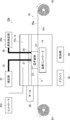
- FIG. 1 is a schematic diagram illustrating an example of an organic semiconductor film manufacturing apparatus according to an embodiment of the present invention.
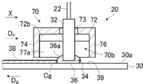
- a manufacturing apparatus 10 shown in FIG. 1 is used in the method for manufacturing an organic semiconductor film according to the embodiment of the present invention, and uses a coating method.
- the stage 14, the temperature controller 16 disposed on the stage 14, the coating member 20, and the coating member 20 are opposite to the first direction X and the first direction X in the interior 12 a of the casing 12.
- a guide rail 26 that moves in the direction is provided.
- the stage 14 and the temperature controller 16 are connected to a driver 18, and the driver 18 controls the movement of a substrate 30 described later by the stage 14 and the temperature of the substrate 30 described later by the temperature controller 16.
- the application member 20 is connected to the supply unit 24 via the supply pipe 22.
- the guide rail 26 is connected to a motor 28, and the application member 20 moves in the direction opposite to the first direction X and the first direction X by the motor 28.
- the driver 18, the supply unit 24 and the motor 28 are connected to the control unit 29, and the driver 18, the supply unit 24 and the motor 28 are controlled by the control unit 29.
- the first direction X and the direction opposite to the first direction X are directions parallel to the surface of the stage 14. Since the substrate 30 is disposed so that the surface 30a of the substrate 30 and the surface of the stage 14 are parallel to the stage 14, the direction parallel to the surface 30a of the substrate 30 is also the first direction X.
- the stage 14 is provided with a temperature controller 16 and a substrate 30.
- the stage 14 can move the substrate 30 in a direction opposite to the first direction X and the first direction X, and the first direction X and the first direction X in a plane parallel to the surface 30a of the substrate 30 (not shown). It is moved in a second direction Y (not shown) that is orthogonal. Furthermore, the stage 14 moves the substrate 30 in the direction opposite to the second direction Y.
- the configuration of the stage 14 is not particularly limited as long as the substrate 30 can be moved in the first direction X and its opposite direction and in the second direction Y and its opposite direction.
- the temperature controller 16 sets the temperature of the substrate 30 to a predetermined temperature and holds the temperature.
- the configuration of the temperature controller 16 is not particularly limited as long as the temperature of the substrate 30 can be set to a predetermined temperature as described above. As the temperature controller 16, for example, a hot plate can be used.
- the coating member 20 is disposed to face and separate from the front surface 30a of the substrate 30 on which the organic semiconductor film 38 (see FIG. 2) is formed, and the organic semiconductor solution reservoir 34 (see FIG. 2) is disposed between the coating member 20 and the substrate 30. ).
- An organic semiconductor solution (see FIG. 2) for forming the organic semiconductor film 38 (see FIG. 2) is supplied from the supply unit 24 between the substrate 30 and the coating member 20, and the organic semiconductor film is applied to the surface 30a of the substrate 30 by the coating member 20. 38 (see FIG. 2) is formed.
- the configuration of the application member 20 will be described later in detail.
- the substrate 30 is not limited to the substrate 30 alone, but when a layer is formed on the surface 30 a of the substrate 30, and when the organic semiconductor film is formed on the surface of the layer, the surface of the layer is the substrate 30. Corresponds to the surface 30a.
- the configuration of the supply pipe 22 connected to the application member 20 is not particularly limited as long as the organic semiconductor solution can be supplied from the supply unit 24 to the application member 20.
- the supply pipe 22 is connected to the application member 20.
- the coating blade 32 is provided so as to penetrate therethrough.
- the supply pipe 22 is preferably flexible so that it can follow when the application member 20 moves.
- the number of supply pipes 22 is not limited to one and may be plural, and is determined as appropriate according to the size of the application member 20, the size of the organic semiconductor film, and the like.
- the supply unit 24 supplies the organic semiconductor solution to the application member 20 as described above.
- a tank (not shown) for storing the organic semiconductor solution and the organic semiconductor solution in the tank to the application member 20 are provided.
- a pump (not shown) for sending out and a flow meter (not shown) for measuring the sending amount of the organic semiconductor solution are provided.
- a syringe pump can be used as the supply unit 24. It is desirable that the supply unit 24 and the supply pipe 22 are heated and adjusted in a timely manner. The temperatures of the supply unit 24 and the supply pipe 22 are desirably set to the same level as the substrate temperature.
- the organic semiconductor solution 36 can be stably supplied by reliably dissolving the organic semiconductor solution 36 by heating. Further, the smaller the temperature difference between the organic semiconductor solution 36 and the substrate 30 during supply, the more stable liquid reservoir 34 can be formed.
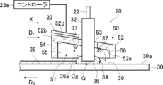
- the manufacturing apparatus 10 may have a configuration in which, for example, a heating unit 23 that heats at least a part of a cover unit described later to a predetermined temperature may be provided.
- the heating unit 23 is connected to the controller 23a.
- the controller 23a heats a cover part described later in the heating part 23.
- the controller 23 a is connected to the control unit 29, and the controller 23 a is controlled by the control unit 29.
- the heating unit 23 is not particularly limited, and for example, a resistance heating type heater is used.
- the heating unit 23 is not necessarily provided.
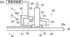
- the manufacturing apparatus 10 may have a configuration in which a vapor supply unit 25a that supplies a vapor of the solvent of the organic semiconductor solution via the pipe 25 is provided in a cover unit described later.
- the vapor supply unit 25a supplies the vapor of the solvent of the organic semiconductor solution to the application member 20 as described above.
- a tank (not shown) that stores the solvent of the organic semiconductor solution, and the organic in the tank A heater (not shown) that vaporizes the solvent of the semiconductor solution is included.
- the solvent vapor may be supplied to the application member 20 with the pressure of the solvent vapor, or the solvent vapor may be supplied to the application member 20 using a blower (not shown).
- the solvent vapor supply method described above is appropriately set according to the amount of the solvent vapor of the organic semiconductor solution, the length of the pipe 25, and the like.
- the pipe 25 is preferably flexible so that it can follow when the application member 20 moves. Note that the vapor supply unit 25a that supplies the vapor of the solvent of the organic semiconductor solution to the application member 20 is not necessarily provided.
- the pipe 25 is preferably heated to the same level as the tank. By heating, dew condensation in the pipe 25 can be suppressed, and the solvent vapor of the organic semiconductor solution can be effectively introduced.
- the guide rail 26 moves the application member 20 in the first direction X and the opposite direction.
- the application member 20 is attached to the guide rail 26 with a carriage 27.
- the carriage 27 can be moved in the first direction X and the opposite direction by the guide rail 26, and the application member 20 moves in the first direction X and the opposite direction together with the carriage 27.
- the carriage 27 is moved by the motor 28 in the first direction X and the opposite direction.
- the position of the carriage 27 can be calculated from a reading value of a linear scale (not shown) provided on the guide rail 26, whereby the position of the application member 20 in the first direction X can be calculated.
- the carriage 27 can change the attachment height and the attachment angle of the application member 20.
- the application member 20 can be moved in the first direction X and the opposite direction, and the substrate 30 can be moved in the first direction X and the opposite direction.
- the first direction X is referred to as the X direction.
- the second direction Y is referred to as the Y direction.
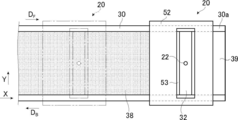
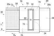
- FIG. 2 is a schematic cross-sectional view showing an application member and a cover part of the organic semiconductor film manufacturing apparatus according to the embodiment of the present invention
- FIG. 3 is a plan view of the application member and the cover part
- FIG. It is typical sectional drawing which shows a modification.
- the coating member 20 has a coating blade 32 formed of a flat plate.
- the coating blade 32 has a flat end surface 32a.
- the coating member 20 is disposed with the end face 32 a of the coating blade 32 parallel to the surface 30 a of the substrate 30.
- the coating blade 32 is disposed so as to be separated from the surface 30 a of the substrate 30, and there is a gap between the end surface 32 a and the surface 30 a of the substrate 30. This gap is the gap G.
- a liquid pool 34 is formed between the coating blade 32 and the surface 30 a of the substrate 30.
- the length d of the gap G is the length from the surface 30 a of the substrate 30 to the end surface 32 a of the coating blade 32. Note that the length d of the gap G is preferably 200 ⁇ m or less.
- the length d of the gap G is measured by the amount by which the carriage 27 is lifted from the state in which the coating blade 32 is in contact with the surface 30a of the substrate 30. If a micrometer (not shown) for height adjustment is installed on the carriage 27, the length d of the gap G can be measured. More precisely, a digital image including the substrate 30 is acquired from the side surface of the coating blade 32, the digital image is taken into a computer, and the surface 30a of the substrate 30 and the corners of the coating blade 32 are based on the digital image. The length up to 32d is measured on the computer.
- the coating member 20 is moved in the DF direction while being in contact with the organic semiconductor solution 36. Further, while contacting the coating member 20 in the organic semiconductor solution 36 in forming the organic semiconductor film 38, the substrate 30 may be moved to the D B direction.
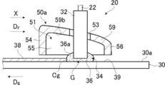
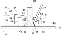
- the coating blade 32 of the coating member 20 is provided with a cover portion 50 that covers at least the crystal growth portion Cg of the organic semiconductor solution 36.
- the crystal growth portion Cg of the organic semiconductor solution 36 is that a region serving as a starting point for the organic semiconductor film 38 is formed, the liquid surface 36a of the organic semiconductor solution 36 D B direction side of the liquid reservoir 34 (see FIG. 2 ) Is a region in contact with the surface 30 a of the substrate 30.
- a digital image including the liquid reservoir 34 and the organic semiconductor film 38 is acquired, and this digital image is taken into a computer. Based on the digital image, the vicinity of the boundary between the liquid reservoir 34 and the organic semiconductor film 38 is obtained.
- the crystal growth part Cg can be specified by visual observation.
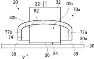
- the cover unit 50 includes a guide to which the solvent of the evaporated organic semiconductor solution 36 adheres and guides the deposit 37 formed by the solvent of the evaporated organic semiconductor solution 36 to the non-film formation region 39 of the organic semiconductor film 38. .
- the structure of the guide is not particularly limited as long as the deposit 37 can be guided to the non-deposition region 39 of the organic semiconductor film 38 as described above.
- the cover part 50 has an inclined part 52 inclined with respect to the surface 30 a of the substrate 30, and flat parts 54 and 56 are provided at each end part in the X direction of the inclined part 52. Further, a side portion 55 is provided at an end portion of the inclined portion 52 in the Y direction.
- the inclined portion 52 has an inclined surface 52b in which the distance from the surface 30a of the substrate 30 is shortened from the crystal growth portion Cg toward the liquid reservoir 34.
- the inclined portion 52 is provided with an opening 53 through which the coating blade 32 passes. As shown in FIG. 2B, there is a gap between the coating blade 32 and the opening 53 at the end in the inclined portion 52Y direction.
- the cover portion 50 covers the periphery of the coating blade 32 including the liquid reservoir 34 and the crystal growth portion Cg.
- the cover portion 50 seals the space above the liquid reservoir 34 and the crystal growth portion Cg.
- the inclined surface 52b has an inclination that makes the distance from the surface 30a of the substrate 30 monotonously shorten.
- the inclined part 52 including the inclined surface 52b is a guide.
- the cover unit 50 is installed on the carriage 27 and moves integrally with the coating blade 32.
- the temperature controller 16 sets the temperature of the substrate 30 to a predetermined temperature. At this time, the solvent of the organic semiconductor solution 36 evaporates, adheres to the inclined surface 52b of the inclined portion 52, and forms dew, and the deposit 37 adheres to the inclined surface 52b of the inclined portion 52.
- the deposit 37 moves in the DF direction along the inclination of the inclined surface 52b by gravity, passes through the side 52c of the inclined portion 52 of the coating blade 32, and is guided to the flat portion 56 side. Since there is no crystal growth portion Cg and organic semiconductor film 38 on the flat portion 56 side, the deposit 37 is suppressed from falling to the crystal growth portion Cg and organic semiconductor film 38 and further to the liquid reservoir 34. Is also suppressed.
- the deposit 37 does not include those in which the solvent of the organic semiconductor solution 36 volatilizes and floats. When the deposit 37 falls on the crystal growth part Cg and the liquid reservoir 34, the crystal growth part Cg and the liquid reservoir 34 vibrate.
- the vibration of the crystal growth portion Cg and the liquid reservoir 34 adversely affects the quality of the organic semiconductor film 38 to be formed, it is preferable that the crystal growth portion Cg and the liquid reservoir 34 are not vibrated. Even if the deposit 37 falls on the surface 30 a of the substrate 30, the surface 30 a of the substrate 30 on the flat portion 56 side is the non-film formation region 39 and is a region where the organic semiconductor film 38 is to be formed. Even if it adheres, formation of the organic semiconductor film 38 is not affected.
- the temperature of the substrate 30 is higher from the viewpoint of film quality such as crystallinity and manufacturing speed.
- the degree of sealing of the space above the crystal growth part Cg can be increased, and even if the temperature of the substrate 30 is increased, the organic semiconductor solution 36 in the interior 51 of the cover part 50 is increased.
- the solvent vapor pressure can be maintained, and the evaporation rate of the solvent can be suppressed. For this reason, the manufacturing speed of the organic semiconductor film 38 can be increased and the productivity can be increased. If the temperature of the substrate 30 is high, the generation probability of the deposit 37 also increases.
- the deposit 37 is guided to the non-film formation region 39, and the adverse effect due to the generation of the deposit 37 accompanying the temperature rise of the substrate 30 is not affected. Avoided. Furthermore, by providing the cover part 50, the degree of sealing of the space above the crystal growth part Cg can be increased, and wind generated by the movement of the coating member 20 or the substrate 30 when forming the organic semiconductor film 38 is generated. The vibration of the crystal growth part Cg can be suppressed without hitting Cg, and the organic semiconductor film 38 can be formed stably. For this reason, when the organic semiconductor film 38 is continuously formed, even if the temperature of the substrate 30 is increased and the moving speed of the coating member 20 or the substrate 30 is increased, a high-quality organic semiconductor film having high crystallinity. 38 can be obtained continuously.
- the inclined portion 59 may have a curved surface 59 b that is curved with respect to the surface 30 a of the substrate 30.
- the curved surface 59b guides the deposit 37 to the flat surface portion 56 side, like the inclined surface 52b.
- the curved surface 59b has an inclination that the distance from the surface 30a of the substrate 30 becomes shorter from the crystal growth part Cg toward the liquid reservoir 34, that is, from the flat part 54 toward the flat part 56.
- the curved surface 59b is a guide.
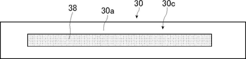
- FIG. 5 is a schematic view showing an example of a substrate used in the organic semiconductor film manufacturing apparatus of the embodiment of the present invention
- FIG. 6 is a plan view for explaining the method of manufacturing the organic semiconductor film of the embodiment of the present invention. It is.
- FIG. 5 for example, when one organic semiconductor film 38 is formed on the surface 30 a of the substrate 30, the region 30 c other than the organic semiconductor film 38 on the surface 30 a of the substrate 30 This is an undeposited region 39. Even if the region where the organic semiconductor film 38 is to be formed, a region where the organic semiconductor film 38 is not yet formed is included in the non-deposited region 39.
- the above-mentioned gap G is provided and the coating member 20 is disposed.
- an organic semiconductor solution 36 is supplied from the supply unit 24 via the supply pipe 22 between the surface 30 a of the substrate 30 and the coating blade 32, and a liquid pool 34 is formed between the coating blade 32 and the surface 30 a of the substrate 30.
- the temperature of the substrate 30 is set to a temperature predetermined by the temperature controller 16 described above.
- the coating member 20 was brought into contact with the organic semiconductor solution 36 between the coating blade 32 of the coating member 20 and the surface 30 a of the substrate 30, that is, while supplying the organic semiconductor solution 36 to the liquid reservoir 34.
- the substrate 30 is moved in the direction DF at a predetermined moving speed.
- the organic semiconductor film 38 is sequentially formed from the crystal growth portion Cg starting from the crystal growth portion Cg of the organic semiconductor solution 36 described above. In this manner, the organic semiconductor film 38 is formed in the direction DF while applying the organic semiconductor solution 36 in the same direction as the direction DF in which the applying member 20 moves, that is, the direction DF .
- the solvent of the organic semiconductor solution 36 evaporates, but the deposit 37 formed with the solvent of the organic semiconductor solution 36 as described above is formed on the crystal growth portion Cg and the film by the inclined surface 52b of the cover portion 50.
- the organic semiconductor film 38 and the liquid reservoir 34 are not dropped. Therefore, a high-quality organic semiconductor film 38 with high crystallinity can be obtained.
- the organic semiconductor film 38 is continuously formed, even when the organic semiconductor film 38 is continuously formed as described above, even if the temperature of the substrate 30 is increased and the moving speed of the coating member 20 or the substrate 30 is increased, the crystal A high-quality organic semiconductor film 38 with high properties can be obtained continuously.
- the supply amount of the organic semiconductor solution 36 is appropriately determined according to the temperature of the substrate 30, the moving speed, the size of the organic semiconductor film 38 to be formed, and the like.
- the application member 20 is moved in the direction DF to form the organic semiconductor film 38.
- the present invention is not limited to this, and the substrate is in contact with the organic semiconductor solution 36 without being limited thereto.
- the organic semiconductor film 38 as described above also is moved in the direction D B can be formed in the direction D F.
- Direction D F is the same direction as the X direction
- the direction D B is the opposite direction of the direction D F.
- the temperature Ts of the substrate 30 is Tb ⁇ 50 ° C. ⁇ Ts ⁇ Tb in the manufacturing process of the organic semiconductor film 38. It is preferred that it be maintained. Within this temperature range, the deposition rate of the organic semiconductor film 38 can be increased, and the productivity of the organic semiconductor film 38 can be increased.
- the temperature Ts of the substrate 30 when forming the organic semiconductor film 38 is more preferably maintained at a temperature of Tb ⁇ 40 ° C. ⁇ Ts ⁇ Tb.
- the moving speed of the application member 20 at the time of formation of the organic semiconductor film 38 is 1 mm / min or more, and the upper limit is, for example, 5 mm / min.
- the moving speed is 1 to 5 mm / min, vibration of the organic semiconductor solution 36 is suppressed by the liquid reservoir 34, and the organic semiconductor film 38 can be formed stably.
- the moving speed of the substrate 30 can be the same as the moving speed of the coating member 20 described above.
- the organic semiconductor film 38 is formed, for example, in the atmosphere and under atmospheric pressure.
- FIG. 7 is a schematic cross-sectional view showing an example of a thin film transistor manufactured using the method for manufacturing an organic semiconductor film according to the embodiment of the present invention.
- a thin film transistor 40 illustrated in FIG. 7 is a bottom-gate, top-contact transistor.
- a gate electrode 43 is formed on the surface 42 a of the substrate 42.
- An insulating film 44 covering the gate electrode 43 is formed on the surface 42 a of the substrate 42.
- An organic semiconductor layer 46 is formed on the surface 44 a of the insulating film 44.
- the organic semiconductor layer 46 is manufactured by the above-described organic semiconductor film manufacturing method.
- a source electrode 48 a and a drain electrode 48 b are formed on the surface 46 a of the organic semiconductor layer 46.
- the organic semiconductor layer 46 is formed on the surface 44a of the insulating film 44.
- the surface 44a of the insulating film 44 corresponds to the surface 30a of the substrate 30 as described above.
- the transistor in which the organic semiconductor film is formed by the organic semiconductor film manufacturing method is not limited to the bottom gate and top contact type thin film transistor 40 shown in FIG. It may be a bottom gate, bottom contact thin film transistor, a top gate, top contact thin film transistor, or a top gate, bottom contact thin film transistor.
- FIG. 8 is a schematic cross-sectional view showing a first example of the arrangement position of the supply pipe in the application member of the organic semiconductor film manufacturing apparatus according to the embodiment of the present invention
- FIG. 9 shows the arrangement position of the supply pipe in the application member. It is a typical sectional view showing the 2nd example.
- the supply pipe 22 is penetrated by the application blade 32 as shown in FIG. 2, but the present invention is not limited to this.
- the supply pipe 22 may be disposed closer to the flat portion 56 than the coating blade 32 of the inclined portion 52 without being provided on the coating blade 32.
- the supply pipe 22 may be disposed on the side of the coating blade 32 that becomes the crystal growth part Cg. Further, as shown in FIG.
- the supply pipe 22 may be arranged on the side surface 32 b opposite to the crystal growth part Cg of the coating blade 32 without being provided on the coating blade 32. Even in the case illustrated in FIG. 9, the supply pipe 22 may be disposed on the side surface of the coating blade 32 on the crystal growth portion Cg side. Note that the number of the supply pipes 22 is not limited to one as described above, and may be plural, and is appropriately determined according to the size of the application member 20, the size of the organic semiconductor film 38, and the like.
- FIG. 10 is a schematic cross-sectional view showing a first example of the cover portion of the organic semiconductor film manufacturing apparatus of the embodiment of the present invention. 10, the same components as those of the application member 20 and the cover unit 50 shown in FIGS. 2 and 3 are denoted by the same reference numerals, and detailed description thereof is omitted.
- the cover unit 50 is provided with a heating unit 23 in a region 52 d facing the crystal growth unit Cg.
- the heating unit 23 is, for example, a resistance heating type heater as described above, and is connected to the controller 23a as described above.
- the cover unit 50 is heated by the heating unit 23. For this reason, even if the solvent of the organic semiconductor solution 36 evaporates and adheres to the cover part 50, the formation of the deposit 37 is suppressed. Even when the deposit 37 formed by the solvent of the evaporated organic semiconductor solution 36 adheres to the inclined surface 52b, the deposit 37 is heated and easily moves along the inclined surface 52b. It is easier to guide on the 56th side. This further suppresses the deposit 37 from falling on the crystal growth part Cg and the organic semiconductor film 38, and further prevents the deposit 37 from falling on the liquid reservoir 34.
- the cover 50 is heated by the heating unit 23, the solvent vapor pressure in the interior 51 is also increased, which is a more preferable state for crystal growth. For this reason, it becomes easier to obtain a high-quality organic semiconductor film 38 with high crystallinity.
- the heating part 23 was provided in the area
- the heating part 23 may be provided in the region 52e on the flat part 56 side of the liquid reservoir 34 in the inclined part 52, and the heating part 23 may be provided on the entire surface of the inclined part 52.
- the heating temperature is preferably equal to or higher than the temperature of the substrate 30.
- FIG. 11 is a schematic cross-sectional view showing a second example of the cover portion of the organic semiconductor film manufacturing apparatus according to the embodiment of the present invention
- FIG. 12 is a plan view of the cover portion of the second example. 11 and 12, the same components as those of the application member 20 and the cover 50 shown in FIGS. 2 and 3 are denoted by the same reference numerals, and detailed description thereof is omitted.
- 11 and 12 is different from the cover portion 50 shown in FIGS. 2 and 3 in that the coating blade 32 and the cover portion 58 are integrated, and other configurations are as follows. It is the same as the cover part 50 shown in FIG. 2 and FIG. As shown in FIGS. 11 and 12, the coating blade 32 and the cover portion 58 are integrated, there is no opening 53, and there is no gap around the coating blade 32.
- the degree of sealing of the space above the crystal growth portion Cg can be increased, and the solvent of the organic semiconductor solution 36 evaporates when the organic semiconductor film 38 is formed. In this case, the solvent vapor pressure in the interior 58a can be kept higher, and the evaporation rate of the solvent can be further suppressed.
- FIG. 13 is a schematic cross-sectional view showing a third example of the cover portion of the organic semiconductor film manufacturing apparatus according to the embodiment of the present invention
- FIG. 14 is a plan view of the cover portion of the third example
- FIG. 9 is a schematic cross-sectional view showing a modification of the cover portion of the third example. 13 to 15, the same components as those of the application member 20 and the cover unit 50 shown in FIGS. 2 and 3 are denoted by the same reference numerals, and detailed description thereof is omitted.
- the coating member 20 and the cover part 50 shown in FIGS. 13 and 14 are piped between the coating blade 32 and the flat part 56 of the cover part 50 as compared with the coating member 20 and the cover part 50 shown in FIGS.
- the steam supply part 25a is connected through 25, and other configurations are the same as those of the coating member 20 and the cover part 50 shown in FIGS.
- the vapor of the solvent of the organic semiconductor solution 36 is supplied into the cover unit 50 by the vapor supply unit 25a.
- the structure provided in the crystal growth part Cg side may be sufficient as the piping 25.
- the vapor of the solvent from the vapor supply unit 25a can increase the solvent vapor pressure, particularly above the crystal growth unit Cg, in the interior 51 and suppress the evaporation rate of the solvent. It is preferable to provide it on the Cg side.
- the number of the pipes 25 is not limited to one, and may be plural, and is appropriately set according to the size of the organic semiconductor film 38 to be formed, the required quality of the organic semiconductor film 38, and the like. Further, it is preferable that the temperature of the vapor of the solvent of the supplied organic semiconductor solution 36 is equal to the temperature of the substrate 30.
- the application member 20 and the cover unit 50 are provided with the heating unit 23 described above, supplied with the vapor of the solvent by the vapor supply unit 25a, and the cover unit 50 and the application blade 32.
- the heating unit 23 described above, supplied with the vapor of the solvent by the vapor supply unit 25a, and the cover unit 50 and the application blade 32.
- at least two may be combined, or all may be combined.
- FIG. 16 is typical sectional drawing which shows the other example of the application member of the manufacturing apparatus of the organic-semiconductor film of embodiment of this invention.
- the same components as those of the application member 20 and the cover unit 50 shown in FIGS. 2 and 3 are denoted by the same reference numerals, and detailed description thereof is omitted.
- the application member 20 shown in FIG. 16 is different from the application member 20 shown in FIGS. 2 and 3 in the configuration of the application blade 60, and the other configurations are the same as those of the application member 20 shown in FIGS. It is.
- the coating blade 60 has an end face 62 that faces the surface 30 a of the substrate 30 inclined with respect to the surface 30 a of the substrate 30.
- the coating member 20 is disposed such that the end surface 62 of the coating blade 60 is separated from the surface 30 a of the substrate 30, and a liquid pool 34 is formed between the end surface 62 of the coating blade 60 and the surface 30 a of the substrate 30.
- the vibration of the liquid pool 34 can be suppressed as compared with the coating blade 32 in which the end face 32a shown in FIG. 2 is parallel to the surface 30a of the substrate 30. Thereby, the organic semiconductor film 38 with higher crystallinity can be obtained.
- the inclination angle ⁇ of the end face 62 of the coating blade 60 with respect to the surface 30a of the substrate 30 is preferably 1 ° to 14 °, for example. More preferably, the inclination angle ⁇ is 1 ° to 9 °, and more preferably 4 ° to 9 °. When the inclination angle ⁇ is 1 ° to 14 °, an appropriate amount of the organic semiconductor solution 36 can be held, and a crystal film with high mobility can be produced at a high moving speed.
- the inclination angle ⁇ of the coating blade 60 described above is an angle formed by the surface 30 a of the substrate 30 and the end surface 62 of the coating blade 60. The length of the coating blade 60 is about 2 cm.
- the temperature of the substrate 30 is Ts ° C.
- the temperature Ts of the substrate 30 is preferably maintained at a temperature of Tb ⁇ 30 ° C. ⁇ Ts ⁇ Tb. Within this temperature range, the deposition rate of the organic semiconductor film 38 can be increased, and the productivity of the organic semiconductor film 38 can be increased.
- the temperature Ts of the substrate 30 when forming the organic semiconductor film 38 is more preferably maintained at a temperature of Tb ⁇ 20 ° C. ⁇ Ts ⁇ Tb.
- the moving speed of the coating blade 60 of the coating member 20 when forming the organic semiconductor film 38 is preferably 5 mm / min or more, more preferably 10 mm / min or more.
- the upper limit value of the moving speed is about 100 mm / min.
- an organic semiconductor film having high crystallinity and mobility can be obtained until the moving speed is about 100 mm / min.
- the moving speed of the substrate 30 is as follows. The moving speed of the coating blade 60 can be made the same.
- the above-described heating unit 23 may be provided, or the solvent vapor may be supplied into the cover unit 50 shown in FIG. 16 by the above-described vapor supply unit 25a. Good.
- the cover unit 50 and the coating blade 32 shown in FIG. 16 may be integrated. Of these, at least two may be combined or all may be combined.
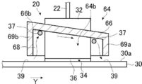
- FIG. 17 is a schematic cross-sectional view showing a fourth example of the cover part of the organic semiconductor film manufacturing apparatus according to the embodiment of the present invention
- FIG. 18 is a front view of the fourth example of the cover part.
- These are typical plane sectional views of the 4th example of a cover part. 17 to 19, the same components as those of the application member 20 and the cover 50 shown in FIGS. 2 and 3 are denoted by the same reference numerals, and detailed description thereof is omitted.
- the cover portion 64 shown in FIGS. 17 to 19 is provided with an inclined surface 66b inclined in the Y direction as compared with the cover portion 50 shown in FIGS. 2 and 3, and the deposit 37 is attached to the organic semiconductor film 38 in the Y direction.
- the structure is the same as that of the coating member 20 and the cover unit 50 shown in FIGS. 2 and 3 except that it is dropped into the non-film formation region 39 on the side.
- the inclined surface 66b is a guide.
- the cover portion 64 is provided with flat portions 68 at both ends of the inclined portion 66 in the X direction.
- the side part 69a and the side part 69b are connected to the end part of the inclined part 66 in the Y direction.
- the inclined portion 66 is inclined so as to monotonously approach the surface 30a of the substrate 30 with respect to the Y direction, and the side portion 69a is shorter than the side portion 69b.
- the inclined portion 66 is provided with an opening 67 into which the coating blade 32 is inserted.
- the cover part 64 covers the periphery of the coating blade 32 including the liquid reservoir 34 and the crystal growth part Cg.
- the cover portion 64 has the inclined surface 66b that is opposed to the crystal growth portion Cg in the cross section in the Y direction orthogonal to the X direction.
- the back surface of the inclined portion 66 is an inclined surface 66 b, and the deposit 37 formed by the solvent of the organic semiconductor solution 36 is guided to the non-deposited region 39 in the Y direction of the organic semiconductor film 38 by the inclined surface 66 b.
- the organic semiconductor film 38 is not formed.
- the deposit 37 can be guided to the non-film formation region 39 similarly to the cover portion 50 of FIGS. 2 and 3, and the crystal quality is high.
- the organic semiconductor film 38 can be obtained.
- the cover part 64 guides the deposit 37 to the undeposited region 39 on the side of the organic semiconductor film 38 where the organic semiconductor film 38 is not formed, and is different from the region where the organic semiconductor film 38 is to be formed in the cover part 50. For this reason, the deposit 37 is not included in the organic semiconductor film 38.
- the cover portion 64 similarly to the cover portion 50, the solvent vapor pressure in the inner portion 64b can be increased, and the evaporation rate of the solvent can be suppressed.
- the above-described heating part 23 may be provided, and the vapor of the solvent may be supplied into the cover part 64 by the above-described vapor supply part 25a.
- the cover part 64 and the coating blade 32 may be integrated. Of these, at least two may be combined or all may be combined.
- FIG. 20 is a schematic cross-sectional view showing a fifth example of the cover part of the organic semiconductor film manufacturing apparatus according to the embodiment of the present invention
- FIG. 21 is a front view of the fifth example of the cover part
- FIG. These are typical plane sectional views of the 5th example of a cover part. 20 to 22, the same components as those of the application member 20 and the cover 50 shown in FIGS. 2 and 3 are denoted by the same reference numerals, and detailed description thereof is omitted.
- the 20 to 22 includes an inclined surface 72b inclined in the Y direction and an inclined surface 72c inclined in the direction opposite to the Y direction, as compared to the cover portion 50 shown in FIGS.
- the difference is that the deposit 37 is dropped into the non-deposited region 39 on the Y direction side of the organic semiconductor film 38 and the non-deposited region 39 on the opposite side to the Y direction.
- the inclined surfaces 72b and 72c are guides.
- the cover portion 70 is provided with flat portions 74 and 76 at both ends in the X direction of the inclined portion 72.
- a side portion 77a and a side portion 77b are provided at the end of the inclined portion 72 in the Y direction.
- the inclined portion 72 is connected to an inclined plate 75 by changing the direction of inclination, and the side portion 77a and the side portion 77b have the same length.
- the back surfaces of the inclined plates 75 are inclined surfaces 72b and 72c.
- the inclined surface 72b is inclined so as to monotonously approach the surface 30a of the substrate 30 in the Y direction.
- the inclined surface 72c is in the opposite direction to the inclined surface 72b, and is inclined so as to approach the surface 30a of the substrate 30 monotonously in the direction opposite to the Y direction.
- the inclined portion 72 is provided with an opening 73 into which the coating blade 32 is inserted.
- the cover portion 70 covers the periphery of the coating blade 32 including the liquid reservoir 34 and the crystal growth portion Cg.
- the inclined surfaces 72b and 72c facing the crystal growth part Cg are inclined in the cross section in the Y direction orthogonal to the X direction.
- the back surfaces of the inclined plates 75 of the inclined portion 72 are inclined surfaces 72b and 72c, and the deposits 37 formed by the solvent of the organic semiconductor solution 36 on the inclined surfaces 72b and 72c and the Y direction of the organic semiconductor film 38 and The film is guided to an undeposited region 39 in the direction opposite to the Y direction.
- the deposit 37 is led to the non-deposition region 39 on the side of the organic semiconductor film 38 where the organic semiconductor film 38 is not formed, and is different from the region where the organic semiconductor film 38 is to be formed in the cover part 50. For this reason, the deposit 37 is not included in the organic semiconductor film 38.
- the cover portion 70 includes the inclined plates 75 having the same inclination angle and different directions, so that the distance until the deposit 37 reaches the non-film formation region 39 is shorter than the cover portion 50 of FIGS. 17 and 18. can do. For this reason, even if the deposit 37 adheres to the upper side of the crystal growth part Cg, it can be further suppressed from falling to the crystal growth part Cg. As with the cover portion 50 of FIGS. 2 and 3, the deposit 37 can be guided to the non-film formation region 39, and a high-quality organic semiconductor film 38 with high crystallinity can be obtained. Further, in the cover part 70 as well as the cover part 50, the solvent vapor pressure in the interior 70b can be increased, and the evaporation rate of the solvent can be suppressed.
- cover unit 70 and the coating blade 32 may be integrated. Of these, at least two may be combined or all may be combined.
- FIG. 23 is a schematic cross-sectional view showing a sixth example of the cover part of the organic semiconductor film manufacturing apparatus of the embodiment of the present invention
- FIG. 24 is a cover part of the organic semiconductor film manufacturing apparatus of the embodiment of the present invention
- FIG. 25 is a schematic cross-sectional view showing a seventh example of the cover part of the organic semiconductor film manufacturing apparatus according to the embodiment of the present invention
- FIG. It is typical sectional drawing which shows the 9th example of the cover part of the manufacturing apparatus of the organic-semiconductor film of embodiment of invention.
- the same components as those of the application member 20 and the cover portion 64 shown in FIGS. 17 and 18 are denoted by the same reference numerals, and detailed description thereof is omitted.
- the cover portion 64a shown in FIG. 23 is different from the cover portion 64 shown in FIGS. 17 and 18 in that the back surface of the inclined portion 80 is a curved surface 80b.
- Other configurations are the same as those shown in FIGS. It is the same as the cover part 64 shown.
- the cover part 64a the curved surface 80b is a guide.
- the inclined portion 80 is curved in an arc shape in the cross section in the Y direction, and the curved surface 59b guides the deposit 37 to the non-deposited region 39 in the Y direction of the organic semiconductor film 38, like the inclined surface 66b. In the Y direction, there is an inclination that makes the distance from the surface 30a of the substrate 30 shorter.
- the solvent vapor pressure in the interior 64b can be increased, and the evaporation rate of the solvent can be suppressed.
- FIG. 24 the same components as those of the application member 20 and the cover unit 70 shown in FIGS. 20 and 21 are denoted by the same reference numerals, and detailed description thereof is omitted.
- the cover part 70a shown in FIG. 24 differs from the cover part 70 shown in FIGS. 20 and 21 in that the back surface of the inclined part 82 is a curved surface 82b.
- Other configurations are the same as those shown in FIGS. It is the same as the cover part 70 shown.
- the curved surface 82b is a guide.
- the inclined portion 82 has an arc shape in the cross section in the Y direction, and the curved surface 82b is configured by, for example, an arc having the longest distance from the intermediate point in the Y direction to the surface 30a of the substrate 30. Similar to the inclined surfaces 72b and 72c, the curved surface 82b guides the deposit 37 to the non-film formation region 39 of the organic semiconductor film 38 in the direction opposite to the Y direction and the Y direction. Also in the cover part 70a, like the cover part 50, the solvent vapor pressure in the interior 70b can be increased, and the evaporation rate of the solvent can be suppressed.
- symbol 54d shown in FIG. 25 shows the lower surface of the plane part 54 in the state which is not inclined.
- the two inclined surfaces 54c exhibit the same function as the two inclined surfaces 72b and 72c in which the direction of the inclination in the Y direction shown in FIG. 21 is changed.
- the manufacturing apparatus 10 is a single wafer type
- the method for manufacturing the organic semiconductor film is not limited to the single wafer type, and may be a roll-to-roll system as in the manufacturing apparatus 10a shown in FIG.
- symbol is attached
- the manufacturing apparatus 10a shown in FIG. 27 is not provided with the stage 14 as compared with the manufacturing apparatus 10 of FIG. 1, and the conveyance form of the substrate 30 is stretched around the unwinding roll 90 and the winding roll 92.
- the coating member 20 is disposed on the front surface 30a side of the substrate 30 and the temperature controller 16 is disposed on the back surface 30b side.
- the rest of the configuration is the same as that of the manufacturing apparatus 10 in FIG.
- the temperature of the substrate 30 is set to a predetermined temperature by the temperature controller 16, and the organic semiconductor film 38 is formed by the coating member 20.
- the coating member 20 may be moved in contact with the organic semiconductor solution 36 (see FIG. 2), and the coating member 20 is moved to the organic semiconductor solution 36 (see FIG. 2).
- the substrate 30 may be taken up by a take-up roll 92 and transported in a state of being in contact with ().
- the coating blade is made of, for example, glass, quartz glass, stainless steel, or the like.
- a glass substrate or a plastic substrate is used as the substrate 30, for example.
- Plastic substrates include, for example, polyesters such as polyethylene terephthalate (PET) and polyethylene naphthalate (PEN), polyethylene (PE), polypropylene (PP), polystyrene, ethylene vinyl acetate (EVA), cycloolefin polymer (COP), cyclohexane It is composed of polyolefins such as olefin copolymer (COC), vinyl resin, polycarbonate (PC), polyamide, polyimide, acrylic resin, triacetyl cellulose (TAC) and the like.
- the plastic substrate does not bend even when bent, and is used, for example, when it is formed by a roll-to-roll method.
- the organic semiconductor solution 36 usually contains at least an organic semiconductor (organic semiconductor compound) and a solvent.
- organic semiconductor organic semiconductor compound
- the kind in particular of an organic semiconductor is not restrict
- pentacenes such as 6,13-bis (triisopropylsilylethynyl) pentacene (TIPS pentacene), tetramethylpentacene, perfluoropentacene, TES-ADT (5,11-bis (triethylsilylethynyl) anthracdi Thiophene), diF-TES-ADT (2,8-difluoro-5,11-bis (triethylsilylethynyl) anthradithiophene) and the like, DPh-BTBT (2,7-diphenyl [1] benzothieno [ 3,2-b] [1] benzothiophene), Cn-BTBT (benzothienobenzothiophen
- the type of solvent is not particularly limited, and alcohol solvents such as methanol and ethanol; ketone solvents such as acetone, methyl ethyl ketone, and methyl isobutyl ketone; aromatic solvents such as benzene and thiophene, and halogens thereof (chlorine) Substituted substances (halogenated aromatic solvents); ether solvents such as tetrahydrofuran and diethyl ether; amide solvents such as dimethylformamide and dimethylacetamide; sulfonic acid solvents such as dimethyl sulfoxide and sulfolane .
- alcohol solvents such as methanol and ethanol
- ketone solvents such as acetone, methyl ethyl ketone, and methyl isobutyl ketone
- aromatic solvents such as benzene and thiophene, and halogens thereof (chlorine) Substituted substances (halogenated aromatic solvents)
- the present invention is basically configured as described above. As mentioned above, although the manufacturing apparatus of the organic-semiconductor film of this invention was demonstrated in detail, this invention is not limited to the above-mentioned embodiment, In the range which does not deviate from the main point of this invention, you may make a various improvement or change. Of course.
- the organic semiconductor film manufacturing apparatus of the present invention will be described more specifically with reference to examples.
- the materials, reagents, used amounts, substance amounts, ratios, processing details, processing procedures, and the like shown in the following examples can be appropriately changed without departing from the spirit of the present invention. Accordingly, the scope of the present invention should not be construed as being limited by the specific examples shown below.
- an organic semiconductor layer composed of an organic semiconductor film was formed using an organic semiconductor film manufacturing apparatus, a thin film transistor was obtained, and thin film transistor element characteristics were evaluated.
- the thin film transistor was manufactured as follows with the channel width W being 1 mm and the channel length L being 50 ⁇ m in the bottom gate and top contact thin film transistor 40 shown in FIG.
- a gate pattern was produced by vacuum deposition using a metal mask.
- a gate electrode having a thickness of 40 nm was formed using Ag (silver).
- a polyimide insulating film having a thickness of 0.5 ⁇ m was formed on the glass substrate by spin coating and cured.
- the glass substrate is placed on a hot plate on the stage, the substrate temperature is set to 100 ° C., and the organic semiconductor solution 36 is applied at a moving speed of 1 mm / min or 5 mm / min to form an organic semiconductor film.
- An organic semiconductor layer was obtained.
- the organic semiconductor solution 36 is obtained by adding C10-DNBDT (3,11-didecyl-dinaphtho [2,3-d: 2 ′, 3′-d ′]-benzo [1,2-b: 4,5-b '] dithiophene), chlorobenzene was used as a solvent, and the solvent concentration was 0.05% by mass.
- an organic semiconductor solution is supplied to form a liquid pool.
- the supply amount of the organic semiconductor solution was adjusted according to the moving speed or the like so that the size of the liquid pool did not change during the application.
- an Au (gold) film having a thickness of 70 nm was formed as a source / drain electrode on the organic semiconductor layer by vacuum deposition using a metal mask.
- type A shown in FIGS. 2 and 3 type B shown in FIG. 17, (b), type C shown in FIGS. 20 and 21, type D shown in FIG. 10, type D, FIG. Type E shown in FIG. 12 and type F shown in FIG. 13B were used.
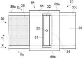
- the cover unit 100 having the configuration shown in FIG. 28 was used. 28, the same components as those of the application member 20 and the cover unit 50 shown in FIGS. 2 and 3 are denoted by the same reference numerals, and detailed description thereof is omitted.
- the cover portion 100 shown in FIG. 28 has flat portions 104 provided at both ends in the X direction of the upper surface portion 102 having a surface 102 b parallel to the surface 30 a of the substrate 30.
- the side part 105 is provided in the edge part of the Y direction of the upper surface part 102, and it is a rectangular parallelepiped shape as a whole.
- the size of the coating member was not limited to the type, and the length of the coating blade was 1 mm and the width of the coating blade was 5 mm.
- the formed organic semiconductor film had a width of 5 mm and a length of 10 cm.
- the dripping was evaluated during the formation of the organic semiconductor film.
- the liquid dripping confirmed the formed organic semiconductor film with the microscope.
- an organic semiconductor crystal that is oriented concentrically like a watermark is observed in the organic semiconductor film.
- the evaluation of the liquid dripping is that the organic semiconductor crystal oriented on the above-mentioned concentric circle is observed as liquid dripping, and the liquid crystal on which the above-mentioned organic semiconductor crystal oriented on the concentric circle is not observed is liquid dripping. It was.
- As for thin film transistor element characteristics saturation mobility was measured for the produced thin film transistor using a semiconductor parameter analyzer (Agilent 4156C). The thin film transistor element characteristics are referred to as “TFT characteristics” in Table 1 below. “ ⁇ ” In the column of TFT characteristics in Table 1 below indicates that saturation mobility was not measured.
- a Saturation mobility ⁇ is 1.0 cm 2 / Vs or more
- b Saturation mobility ⁇ is 0.5 cm 2 / Vs or more and less than 1.0 cm 2 / Vs
- c Saturation mobility ⁇ is 0.01 cm 2 / Vs or more and less than 0.5 cm 2 / Vs
- Saturation mobility ⁇ is 0.01 cm 2 Less than / Vs
- Examples 1 to 12 no dripping occurred and the thin film transistor element characteristics were good. From this, it is clear that the organic semiconductor film manufacturing apparatus of the present invention was able to manufacture a high-quality organic semiconductor film having high crystallinity and mobility.
- an adhering substance was led to the formation region of the organic semiconductor film, and good thin film transistor element characteristics were obtained.
- Examples 2, 3, 8, and 9 lead an adhering substance to the side of the organic semiconductor film, and better thin film transistor element characteristics were obtained.
- Examples 4 and 10 have a heating part in the cover part, and it was possible to suppress adhesion of deposits and to increase the internal solvent vapor pressure, so the film quality of the organic semiconductor film became better, Furthermore, good thin film transistor element characteristics were obtained.
- Comparative Example 2 there was no cover part and no dripping occurred, but the organic semiconductor film with good film quality could not be formed at the set moving speed, and the thin film transistor element characteristics were poor.
- Comparative Example 3 when there was no cover portion, when the moving speed was increased, the characteristics of the thin film transistor element were deteriorated as compared with Examples 7-12.
Landscapes
- Engineering & Computer Science (AREA)
- Manufacturing & Machinery (AREA)
- Liquid Deposition Of Substances Of Which Semiconductor Devices Are Composed (AREA)
- Thin Film Transistor (AREA)
Abstract
Description
カバー部のガイドは、基板の表面と平行な面内で第1の方向と直交する第2の方向の断面において結晶成長部と対向する傾斜面であることが好ましい。
また、カバー部の少なくとも一部を加熱する加熱部を有することが好ましい。加熱部は、カバー部の結晶成長部に対向する領域を加熱することが好ましい。
さらには、塗布部材とカバー部は一体化されていることが好ましい。
有機半導体溶液は溶媒が含まれており、溶媒の蒸気をカバー部の内部に供給する蒸気供給部を有することが好ましい。
また、例えば、塗布部材は端面が基板の表面に対して傾斜した塗布ブレードを有し、塗布部材は塗布ブレードの端面を基板の表面と離間して配置され、塗布ブレードの端面と、基板の表面との間に液溜りが形成される構成とすることもできる。
なお、以下において数値範囲を示す「~」とは両側に記載された数値を含む。例えば、εが数値α~数値βとは、εの範囲は数値αと数値βを含む範囲であり、数学記号で示せばα≦ε≦βである。
「平行」および「直交」等の角度には、厳密な角度に対して、その技術分野で一般的に許容される誤差範囲が含まれる。
図1に示す製造装置10は、本発明の実施形態の有機半導体膜の製造方法に用いられるものであり、塗布法を用いるものである。
ステージ14と温度コントローラ16とはドライバ18に接続されており、ドライバ18により、ステージ14による後述の基板30の移動、および温度コントローラ16による後述の基板30の温度が制御される。塗布部材20は供給管22を介して供給部24に接続されている。
ガイドレール26はモータ28に接続されており、モータ28により、塗布部材20が第1の方向Xと第1の方向Xの反対方向に移動する。
ドライバ18、供給部24およびモータ28は制御部29に接続されており、ドライバ18、供給部24およびモータ28は制御部29で制御される。
ステージ14は基板30を上述の第1の方向Xとその反対方向、および第2の方向Yとその反対方向に移動させることができれば、その構成は特に限定されるものではない。
温度コントローラ16は、基板30の温度を予め定められた温度にし、その温度を保持するものである。温度コントローラ16は、上述のように基板30の温度を予め定められた温度にすることができれば、その構成は特に限定されるものではない。温度コントローラ16には、例えば、ホットプレートを用いることができる。
なお、基板30とは、基板30単体のみならず、基板30の表面30aに層が形成されている場合、その層の表面に有機半導体膜を形成する場合には、その層の表面が基板30の表面30aに相当する。
供給部24は、上述のように塗布部材20に有機半導体溶液を供給するものであり、例えば、有機半導体溶液を貯留するタンク(図示せず)と、タンク内の有機半導体溶液を塗布部材20に送出するポンプ(図示せず)と、有機半導体溶液の送出量を測定する流量計(図示せず)を有する。供給部24としては、例えば、シリンジポンプを用いることができる。
供給部24、供給管22は適時加熱温調していることが望ましい。供給部24および供給管22の温度は望ましくは基板温度と同程度の温度とする。加熱により有機半導体溶液36を確実に溶解させておくことにより安定的に有機半導体溶液36の供給ができる。また、供給時に有機半導体溶液36と基板30との温度差が小さいほど、安定した液溜り34を形成できる。
蒸気供給部25aは、上述のように塗布部材20に有機半導体溶液の溶媒の蒸気を供給するものであり、例えば、有機半導体溶液の溶媒を貯留するタンク(図示せず)と、タンク内の有機半導体溶液の溶媒を蒸気にするヒータ(図示せず)を有する。溶媒の蒸気は、溶媒の蒸気の圧力で塗布部材20に送気してもよく、ブロア(図示せず)を用いて溶媒の蒸気を塗布部材20に送気してもよい。上述の溶媒の蒸気の送気方式は、有機半導体溶液の溶媒の蒸気量、配管25の長さ等に応じて適宜設定されるものである。配管25は塗布部材20が移動する際に、追従できるように可撓性があるものであることが好ましい。なお、塗布部材20に有機半導体溶液の溶媒の蒸気を供給する蒸気供給部25aは必ずしも設ける必要はない。
配管25はタンク同等に加熱するのが好ましい。加熱により、配管25内への結露を抑制し、有機半導体溶液の溶媒の蒸気を効果的に導入することができる。
キャリッジ27はガイドレール26により第1の方向Xとその反対方向に移動可能であり、塗布部材20はキャリッジ27とともに第1の方向Xとその反対方向に移動する。キャリッジ27はモータ28により、第1の方向Xとその反対方向に移動される。
キャリッジ27の位置はガイドレール26に設けられたリニアスケール(図示せず)の読み取り値から算出することができ、これにより、塗布部材20の第1の方向Xにおける位置を算出することができる。キャリッジ27は、塗布部材20の取り付け高さと、取り付け角度を変えることができるものである。
図2は本発明の実施形態の有機半導体膜の製造装置の塗布部材およびカバー部を示す模式的断面図であり、図3は塗布部材およびカバー部の平面図であり、図4はカバー部の変形例を示す模式的断面図である。
塗布部材20は、図2および図3に示すように、平板で構成された塗布ブレード32を有する。塗布ブレード32は、端面32aが平面である。塗布部材20は、塗布ブレード32の端面32aを基板30の表面30aと平行にして配置される。また、塗布ブレード32は、基板30の表面30aと離間して配置されており、端面32aと基板30の表面30aの隙間がある。この隙間がギャップGである。塗布ブレード32と基板30の表面30aの間に液溜り34が形成される。
ギャップGの長さdは、基板30の表面30aと塗布ブレード32の端面32a迄の長さのことである。なお、ギャップGの長さdは、200μm以下が好ましい。
また、より正確には、塗布ブレード32の側面から基板30を含むデジタル画像を取得し、このデジタル画像をコンピュータに取り込み、そのデジタル画像を基に、基板30の表面30aと塗布ブレード32の角部32d迄の長さをコンピュータ上で測定する。
なお、有機半導体膜38を形成する際には塗布部材20を有機半導体溶液36に接した状態で、DF方向に移動させる。また、有機半導体膜38を形成する際には塗布部材20を有機半導体溶液36に接した状態で、基板30をDB方向に移動させてもよい。
有機半導体溶液36の結晶成長部Cgとは、有機半導体膜38が形成される起点となる領域のことであり、液溜り34のDB方向側で有機半導体溶液36の液面36a(図2参照)が基板30の表面30aと接する領域である。
結晶成長部Cgについては、液溜り34と有機半導体膜38を含むデジタル画像を取得し、このデジタル画像をコンピュータに取り込み、そのデジタル画像を基に、液溜り34と有機半導体膜38の境界近傍を目視観察することで、結晶成長部Cgを特定することができる。
カバー部50は、基板30の表面30aに対して傾斜した傾斜部52を有し、傾斜部52のX方向における各端部に平面部54、56が設けられている。また、傾斜部52のY方向の端部にサイド部55が設けられている。傾斜部52は、結晶成長部Cgから液溜り34に向かうにつれて基板30の表面30aとの距離が短くなる傾斜面52bを有する。
また、傾斜部52には、塗布ブレード32が貫通する開口部53が設けられている。図2(b)に示すように、傾斜部52Y方向の端には、塗布ブレード32と開口部53の間に隙間がある。カバー部50により、塗布ブレード32の周囲が液溜り34、結晶成長部Cgを含め覆われており、カバー部50により、液溜り34、結晶成長部Cgの上方の空間が密閉される。
なお、傾斜面52bは、基板30の表面30aとの距離が単調に短くなる傾斜を備えることが好ましい。カバー部50では、傾斜面52bを含め傾斜部52がガイドである。カバー部50はキャリッジ27に設置されており、塗布ブレード32と一体となって動く。
なお、付着物37には、有機半導体溶液36の溶媒が揮発して浮遊するものは含まれない。
結晶成長部Cgおよび液溜り34に付着物37が落下すると、結晶成長部Cgおよび液溜り34が振動する。結晶成長部Cgおよび液溜り34の振動は形成する有機半導体膜38の膜質に悪影響を及ぼすため、結晶成長部Cgおよび液溜り34は振動させないことが好ましい。
また、付着物37が基板30の表面30aに落下しても、平面部56側の基板30の表面30aは未成膜領域39であり、有機半導体膜38の形成予定領域であるが、付着物37が付着していても、有機半導体膜38の形成には影響がない。
さらには、カバー部50を設けることで、結晶成長部Cgの上方の空間の密閉度を高くでき、有機半導体膜38形成時の塗布部材20または基板30の移動に伴い発生する風が結晶成長部Cgに当たらず、結晶成長部Cgの振動を抑制することができ、有機半導体膜38を安定して形成することができる。
このようなことから、有機半導体膜38を連続形成する場合に、基板30の温度を高くして、塗布部材20または基板30の移動速度を速くしても、結晶性が高い良質の有機半導体膜38を連続して得ることができる。
図5は本発明の実施形態の有機半導体膜の製造装置に用いられる基板の一例を示す模式図であり、図6は本発明の実施形態の有機半導体膜の製造方法を説明するための平面図である。
図5に示すように、基板30の表面30aに対して、例えば、1つの有機半導体膜38を形成する場合、基板30の表面30aにおいて有機半導体膜38以外の領域30cは、有機半導体膜38の未成膜領域39である。なお、有機半導体膜38の形成予定領域であっても、まだ有機半導体膜38が形成されていない領域は未成膜領域39に含まれる。
次に、基板30の表面30aと塗布ブレード32の間に、供給部24から供給管22を介して有機半導体溶液36を供給し、塗布ブレード32と基板30の表面30aの間に液溜り34を形成する。このとき、基板30の温度は、上述の温度コントローラ16で予め定められた温度にされている。
有機半導体膜38を連続形成する場合、上述のように有機半導体膜38を連続形成する場合に、基板30の温度を高くして、塗布部材20または基板30の移動速度を速くしても、結晶性が高い良質の有機半導体膜38を連続して得ることができる。
なお、有機半導体溶液36の供給量は、基板30の温度、移動速度、形成する有機半導体膜38の大きさ等に応じて適宜決定されるものである。
方向DFは、X方向と同じ方向であり、方向DBは方向DFの逆方向である。
有機半導体膜38形成時の基板30の温度Tsは、より好ましくはTb-40℃≦Ts≦Tbの温度に保たれている。
また、有機半導体膜38の形成時の塗布部材20の移動速度は、1mm/分以上であることが好ましく、上限としては、例えば、5mm/分である。移動速度が1~5mm/分であれば、液溜り34で有機半導体溶液36の振動が抑制され、有機半導体膜38を安定して成膜することできる。なお、有機半導体膜38の形成時に基板30を移動させる場合には、基板30の移動速度は、上述の塗布部材20の移動速度と同じにすることができる。
また、有機半導体膜38の形成は、例えば、大気中、大気圧下でなされる。
図7は本発明の実施形態の有機半導体膜の製造方法を利用して製造される薄膜トランジスタの一例を示す模式的断面図である。
図7に示す薄膜トランジスタ40はボトムゲート、トップコンタクト型のトランジスタである。薄膜トランジスタ40は、基板42の表面42aにゲート電極43が形成されている。このゲート電極43を覆う絶縁膜44が基板42の表面42aに形成されている。絶縁膜44の表面44aに有機半導体層46が形成されている。この有機半導体層46が、上述の有機半導体膜の製造方法で製造される。有機半導体層46の表面46aにソース電極48aとドレイン電極48bが形成されている。
なお、薄膜トランジスタ40では、絶縁膜44の表面44aに有機半導体層46が形成されているが、この場合、上述のように、絶縁膜44の表面44aが基板30の表面30aに相当する。
塗布部材20では供給管22が図2に示すように、塗布ブレード32に貫通されているが、これに限定されるものではない。図8に示すように塗布ブレード32に設けることなく、傾斜部52の塗布ブレード32よりも平面部56側に供給管22を配置してもよい。なお、塗布ブレード32の結晶成長部Cgとなる側に供給管22を配置してもよい。
また、図9に示すように塗布ブレード32に設けることなく、塗布ブレード32の結晶成長部Cgとは反対側の側面32bに供給管22を配置してもよい。図9に示す場合でも、供給管22は塗布ブレード32の結晶成長部Cg側の側面に配置してもよい。
なお、供給管22の配置数は、上述のように1つに限定されるものではなく複数でもよく、塗布部材20の大きさ、有機半導体膜38の大きさ等に応じて適宜決定される。
ここで、図10は本発明の実施形態の有機半導体膜の製造装置のカバー部の第1の例を示す模式的断面図である。
なお、図10において、図2および図3に示す塗布部材20およびカバー部50と同一構成物には、同一符号を付してその詳細な説明は省略する。
加熱部23は、例えば、上述のように抵抗加熱方式のヒータであり、上述のようにコントローラ23aに接続されている。カバー部50が加熱部23で加熱される。このため、有機半導体溶液36の溶媒が蒸発してカバー部50に付着しても、付着物37が形成されること自体が抑制される。傾斜面52bに、蒸発した有機半導体溶液36の溶媒で形成される付着物37が付着した場合でも、付着物37が加熱され、傾斜面52bに沿って移動しやすくなり、付着物37を平面部56側により導きやすくなる。これにより、付着物37が結晶成長部Cgおよび有機半導体膜38に落下することが更に抑制され、さらには液溜り34に落下することも更に抑制される。
なお、加熱部23を結晶成長部Cgに対向する領域52dに設けたが、これに限定されるものではなく、加熱部23は少なくとも一部を加熱するものである。加熱部23は傾斜部52において液溜り34の平面部56側の領域52eに設けてもよく、更には傾斜部52全面に加熱部23を設けてもよい。
加熱部23でカバー部50を加熱する際、加熱温度は基板30の温度以上であることが好ましい。
なお、図11および図12において、図2および図3に示す塗布部材20およびカバー部50と同一構成物には、同一符号を付してその詳細な説明は省略する。
図11および図12に示すように塗布ブレード32とカバー部58は一体化されており、開口部53がなく、塗布ブレード32の周囲に隙間がない。隙間なく塗布ブレード32とカバー部58を一体にすることで、結晶成長部Cgの上方の空間の密閉度を高くすることができ、有機半導体膜38の形成時、有機半導体溶液36の溶媒が蒸発した際、内部58aの溶媒蒸気圧をより高く保つことができ、溶媒の蒸発速度をより抑えることができる。これにより、結晶性がより高い有機半導体膜38をより得やすい。
また、カバー部58は隙間がないため、溶媒の蒸気が外部に漏れることが抑制されるため、内部58aの溶媒蒸気圧の変動も抑制され、有機半導体膜38を安定にして形成することができる。
なお、図13~図15において、図2および図3に示す塗布部材20およびカバー部50と同一構成物には、同一符号を付してその詳細な説明は省略する。
蒸気供給部25aにより、例えば、有機半導体溶液36の溶媒の蒸気がカバー部50内に供給される。これにより、有機半導体膜38の形成時、内部51の溶媒蒸気圧を高くすることができ、有機半導体溶液36の溶媒の蒸発速度を抑えることができる。これにより、結晶性がより高い有機半導体膜38を得ることができる。
配管25の数は、1つに限定されるものではなく、複数でもよく、形成する有機半導体膜38の大きさ、要求される有機半導体膜38の品質等に応じて適宜設定される。また、供給される有機半導体溶液36の溶媒の蒸気の温度は、基板30の温度と同等であることが好ましい。
なお、図2および図3に示す塗布部材20およびカバー部50では、上述の加熱部23を設けること、上述の蒸気供給部25aによる溶媒の蒸気を供給すること、およびカバー部50と塗布ブレード32を一体にすることのうち、少なくとも2つを組み合わせてもよく、全部組み合わせてもよい。
なお、図16において、図2および図3に示す塗布部材20およびカバー部50と同一構成物には、同一符号を付してその詳細な説明は省略する。
塗布ブレード60は基板30の表面30aと対向する端面62が、基板30の表面30aに対して傾斜している。塗布部材20は塗布ブレード60の端面62を基板30の表面30aと離間して配置され、塗布ブレード60の端面62と、基板30の表面30aとの間に液溜り34が形成される。
塗布ブレード60の端面62を傾斜させることにより、図2に示す端面32aが基板30の表面30aと平行な塗布ブレード32に比して、液溜り34の振動を抑えることができる。これにより、結晶性がより高い有機半導体膜38を得ることができる。
傾斜角度θが1°~14°であれば、適量の有機半導体溶液36を保持でき、移動度が高い結晶膜を速い移動速度で作製することができる。上述の塗布ブレード60の傾斜角度θは、基板30の表面30aと塗布ブレード60の端面62とのなす角度である。また、塗布ブレード60の長さは2cm程度である。
有機半導体膜38形成時の基板30の温度Tsは、より好ましくはTb-20℃≦Ts≦Tbの温度に保たれている。
また、有機半導体膜38の形成時の塗布部材20の塗布ブレード60の移動速度は、5mm/分以上であることが好ましく、より好ましくは10mm/分以上である。移動速度が5mm/分以上であれば、有機半導体膜38について速い成膜速度が得られ、生産性を高くすることができる。なお、上述の移動速度の上限値は100mm/分程度であり、斜めの塗布ブレード60では、移動速度が100mm/分程度迄は結晶性および移動度が高い有機半導体膜を得ることができる。図16に示す構成で、有機半導体膜38の形成時に塗布部材20を有機半導体溶液36に接した状態で、基板30を移動させる場合には、基板30の移動速度は、上述の塗布部材20の塗布ブレード60の移動速度と同じにすることができる。
なお、図17~図19において、図2および図3に示す塗布部材20およびカバー部50と同一構成物には、同一符号を付してその詳細な説明は省略する。
このように、傾く向きがY方向のカバー部64であっても、図2および図3のカバー部50と同様に付着物37を未成膜領域39に導くことができ、結晶性が高い良質の有機半導体膜38を得ることができる。
カバー部64は、付着物37を有機半導体膜38が形成されない、有機半導体膜38の脇に未成膜領域39に導くものであり、カバー部50の有機半導体膜38の形成予定領域とは異なる。このため、付着物37が有機半導体膜38に含まれることがない。
図17および図18に示すカバー部64でも、上述の加熱部23を設けてもよく、また、上述の蒸気供給部25aにより溶媒の蒸気をカバー部64内に供給してもよい。さらには、カバー部64と塗布ブレード32を一体にしてもよい。これらのうち、少なくとも2つを組み合わせてもよく、全部組み合わせてもよい。
なお、図20~図22において、図2および図3に示す塗布部材20およびカバー部50と同一構成物には、同一符号を付してその詳細な説明は省略する。
傾斜部72の各傾斜板75の裏面が傾斜面72b、72cであり、この傾斜面72b、72cで、有機半導体溶液36の溶媒で形成される付着物37が、有機半導体膜38のY方向およびY方向の反対方向の未成膜領域39に導かれる。カバー部70でも、付着物37を有機半導体膜38が形成されない、有機半導体膜38の脇に未成膜領域39に導くものであり、カバー部50の有機半導体膜38の形成予定領域とは異なる。このため、付着物37が有機半導体膜38に含まれることがない。
また、カバー部70でも、カバー部50と同様に内部70bの溶媒蒸気圧を高くでき、溶媒の蒸発速度を抑制することができる。
図20および図21に示すカバー部70でも、上述の加熱部23を設けてもよく、また、上述の蒸気供給部25aにより溶媒の蒸気をカバー部70内に供給してもよい。さらには、カバー部70と塗布ブレード32を一体にしてもよい。これらのうち、少なくとも2つを組み合わせてもよく、全部組み合わせてもよい。
なお、図23において、図17および図18に示す塗布部材20およびカバー部64と同一構成物には、同一符号を付してその詳細な説明は省略する。
傾斜部80はY方向の断面において円弧状に湾曲しており、曲面59bは、傾斜面66bと同じく、付着物37を有機半導体膜38のY方向の未成膜領域39に導くものである。Y方向において基板30の表面30aとの距離が短くなる傾斜を備えている。
カバー部64aでも、カバー部50と同様に内部64bの溶媒蒸気圧を高くでき、溶媒の蒸発速度を抑制することができる。
図24に示すカバー部70aは、図20および図21に示すカバー部70に比して、傾斜部82の裏面が曲面82bである点が異なり、それ以外の構成は、図20および図21に示すカバー部70と同じである。カバー部70aでは、曲面82bがガイドである。
図20のカバー部70、および図24のカバー部70aでも、さらに上述の結晶成長部Cgから液溜り34に向かうにつれて基板30の表面30aとの距離が短くなる斜面を組み合わせてもよい。
カバー部70aでも、カバー部50と同様に内部70bの溶媒蒸気圧を高くでき、溶媒の蒸発速度を抑制することができる。
図25に示すカバー部50aのように、平面部54の下面54bをY方向に傾斜する斜面としてもよい。平面部54の下面54bは、図18に示すY方向に傾斜する傾斜面66bと同様の機能を発揮する。これにより、平面部54の内面54aに付着物37が付着した場合、内面54aに沿って付着物37が有機半導体膜38の方に落下しても下面54bにより、Y方向に沿ってガイドされて、付着物37は有機半導体膜38の脇に導かれる。
なお、図25に示す符号54dは、傾斜していない状態の平面部54の下面を示す。
また、図26に示すカバー部50bのように、平面部54の下面を傾斜の向きを変えた2つの斜面54cで構成してもよい。2つの斜面54cは、図21に示すY方向の傾斜の向きを変えた2つの傾斜面72b、72cと同様の機能を発揮する。これにより、平面部54の内面54aに付着物37が付着した場合、内面54aに沿って付着物37が有機半導体膜38の方に落下しても2つの斜面54cにより、Y方向に沿ってガイドされて、付着物37は有機半導体膜38の脇に導かれる。なお、2つの斜面54cは、傾斜角度は同じでもよく、異なっていてもよい。
なお、図27の製造装置10aにおいて、図1に示す製造装置10と同一構成物には、同一符号を付して、その詳細な説明は省略する。
図27に示す製造装置10aは、図1の製造装置10に比して、ステージ14が設けられておらず、基板30の搬送形態が巻出しロール90と巻取りロール92に張架されており、基板30の表面30a側に塗布部材20が配置され、裏面30b側に温度コントローラ16が配置されている点が異なり、それ以外の構成は図1の製造装置10と同様の構成である。
図27の製造装置10aでは、温度コントローラ16で基板30の温度が、予め定められた温度にされて塗布部材20により有機半導体膜38が成膜される。なお、有機半導体膜38の成膜の際には、塗布部材20を有機半導体溶液36(図2参照)に接した状態で移動させてもよく、塗布部材20が有機半導体溶液36(図2参照)に接した状態で基板30を巻取りロール92で巻き取って搬送させてもよい。
塗布ブレードは、例えば、ガラス、石英ガラス、ステンレス鋼等で構成される。
基板30には、例えば、ガラス基板、プラスチック基板が用いられる。
プラスチック基板は、例えば、ポリエチレンテレフタレート(PET)、ポリエチレンナフタレート(PEN)等のポリエステル類、ポリエチレン(PE)、ポリプロピレン(PP)、ポリスチレン、エチレンビニルアセテート(EVA)、シクロオレフィンポリマー(COP)、シクロオレフィンコポリマー(COC)等のポリオレフィン類、ビニル系樹脂、その他、ポリカーボネート(PC)、ポリアミド、ポリイミド、アクリル樹脂、トリアセチルセルロース(TAC)等で構成される。プラスチック基板は、曲げても折れ曲がらないものであり、例えば、ロールツーロール方式で形成する場合に用いられる。
有機半導体の種類は特に制限されず、公知の有機半導体を使用することができる。具体的には、6,13-ビス(トリイソプロピルシリルエチニル)ペンタセン(TIPSペンタセン)、テトラメチルペンタセン、パーフルオロペンタセン等のペンタセン類、TES-ADT(5,11-ビス(トリエチルシリルエチニル)アントラジチオフェン)、diF-TES-ADT(2,8-ジフルオロ-5,11-ビス(トリエチルシリルエチニル)アントラジチオフェン)等のアントラジチオフェン類、DPh-BTBT(2,7-ジフェニル[1]ベンゾチエノ[3,2-b][1]ベンゾチオフェン)、Cn-BTBT(ベンゾチエノベンゾチオフェン)等のベンゾチエノベンゾチオフェン類、C10-DNBDT(3,11-didecyl-dinaphtho[2,3-d:2’,3’-d’]-benzo[1,2-b:4,5-b’]dithiophene)、Cn-DNTT(dinaphtho[2,3-b:2',3'-f]thieno[3,2-b]thiophene)等のジナフトチエノチオフェン類、ペリキサンテノキサンテン等のジオキサアンタントレン類、ルブレン類、C60、PCBM([6,6]-Phenyl-C61-Butyric Acid Methyl Ester)等のフラーレン類、銅フタロシアニン、フッ素化銅フタロシアニン等のフタロシアニン類、P3RT(ポリ(3-アルキルチオフェン))、PQT(ポリ[5,5'-ビス(3-ドデシル-2-チエニル1)-2,2'-ビチオフェン])、P3HT(ポリ(3-ヘキシルチオフェン))等のポリチオフェン類、ポリ[2,5-ビス(3-ドデシルチオフェン-2-イル)チエノ[3,2-b]チオフェン](PBTTT)等のポリチエノチオフェン類等が例示される。
また、溶媒の種類も特に制限されず、メタノール、エタノール等のアルコール系溶媒;アセトン、メチルエチルケトン、メチルイソブチルケトン等のケトン系溶媒;ベンゼン、チオフェン等の芳香族系溶剤、および、それらのハロゲン(塩素、臭素等)置換体(ハロゲン化芳香族系溶媒);テトラヒドロフラン、ジエチルエーテル等のエーテル系溶媒;ジメチルホルムアミド、ジメチルアセトアミド等のアミド系溶媒;ジメチルスルホキシド、スルホラン等のスルホン酸系溶媒等が挙げられる。
本実施例では、有機半導体膜の製造装置を用いて、有機半導体膜で構成される有機半導体層を形成して、薄膜トランジスタを得、薄膜トランジスタ素子特性を評価した。
まず、ガラス基板を洗浄した後、メタルマスクを用いた真空蒸着によりゲートパターンを作製した。密着層として厚さ10nmのCr(クロム)を蒸着した後、Ag(銀)を用いて厚さ40nmのゲート電極を形成した。
次に、厚さ0.5μmのポリイミド絶縁膜をスピンコートにてガラス基板上に塗布し、硬化することで形成した。
次に、ガラス基板をステージ上のホットプレートに設置し、基板温度を100℃にし、移動速度、1mm/分または5mm/分にて、有機半導体溶液36の塗布を行い、有機半導体膜を形成し、有機半導体層を得た。
有機半導体溶液36は、有機半導体にC10-DNBDT(3,11-didecyl-dinaphtho[2,3-d:2’,3’-d’]-benzo[1,2-b:4,5-b’]dithiophene)を用い、溶媒にクロロベンゼンを用い、溶媒濃度を0.05質量%とした。
次に、有機半導体層上に、メタルマスクを用いた真空蒸着法により、厚さ70nmのAu(金)膜をソースドレイン電極として形成した。
比較例には、図28に示す構成のカバー部100を用いた。なお、図28において、図2および図3に示す塗布部材20およびカバー部50と同一構成物には、同一符号を付してその詳細な説明は省略する。
図28に示すカバー部100は、基板30の表面30aと平行な面102bを有する上面部102のX方向の両端に平面部104が設けられている。上面部102のY方向の端部にサイド部105が設けられており、全体で長方体状である。
塗布部材の大きさは、タイプによらず、塗布ブレードの長さを1mmとし、塗布ブレードの幅を5mmとした。また、形成した有機半導体膜は幅が5mm、長さが10cmであった。
薄膜トランジスタ素子特性は、作製した薄膜トランジスタを、半導体パラメータアラナイザ(Agilent製 4156C)を用いて、飽和移動度を測定した。なお、薄膜トランジスタ素子特性のことを下記表1では「TFT特性」と記す。下記表1のTFT特性の欄における「-」は飽和移動度を測定しなかったことを示す。
a 飽和移動度μが1.0cm2/Vs以上、
b 飽和移動度μが0.5cm2/Vs以上1.0cm2/Vs未満
c 飽和移動度μが0.01cm2/Vs以上0.5cm2/Vs未満
d 飽和移動度μが0.01cm2/Vs未満
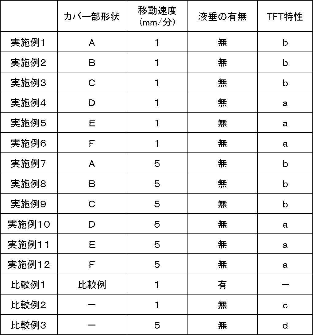
実施例1、7は、有機半導体膜の形成領域に付着物を導くものであり、良好な薄膜トランジスタ素子特性が得られた。実施例2、3、8、9は、有機半導体膜の脇に付着物を導くものであり、より良好な薄膜トランジスタ素子特性が得られた。
実施例4、10はカバー部に加熱部を有するものであり、付着物の付着を抑制でき、かつ内部の溶媒蒸気圧を高くすることができたため、有機半導体膜の膜質がより良いものとなり、更に良好な薄膜トランジスタ素子特性が得られた。
実施例6、12はカバー部に蒸気供給部を有するものであり、内部の溶媒蒸気圧をより高くでき、溶媒の蒸発速度をより抑えることができたため、有機半導体膜の膜質がより良いものとなり、更に良好な薄膜トランジスタ素子特性が得られた。
比較例1は、液垂が生じ、飽和移動度を測定せず、薄膜トランジスタ素子特性を評価しなかった。
比較例2は、カバー部がなく、液垂は生じないが、設定された移動速度では、膜質が良い有機半導体膜を形成することができず、薄膜トランジスタ素子特性が悪かった。
比較例3は、カバー部がない場合、移動速度を速くすると実施例7~12と比較して薄膜トランジスタ素子特性の低下が見られた。
12 ケーシング
12a 内部
14 ステージ
16 温度コントローラ
18 ドライバ
20 塗布部材
22 供給管
23 加熱部
23a コントローラ
24 供給部
25 配管
25a 蒸気供給部
26 ガイドレール
27 キャリッジ
28 モータ
29 制御部
30、42 基板
30a 表面
30b 裏面
30c 領域
32、60 塗布ブレード
32a 端面
32b 側面
32d 角部
34 液溜り
36 有機半導体溶液
36a 液面
37 付着物
38 有機半導体膜
39 未成膜領域
40 薄膜トランジスタ
42a 表面
43 ゲート電極
44 絶縁膜
44a 表面
46 有機半導体層
46a 表面
48a ソース電極
48b ドレイン電極
50、50a、50b、64、70 カバー部
52、59、66、72、80、82 傾斜部
Cg 結晶成長部
DB、DF 方向
G ギャップ
X 第1の方向
Y 第2の方向
θ 傾斜角度
Claims (10)
- 有機半導体溶液を用いて有機半導体膜を製造する有機半導体膜の製造装置であって、
前記有機半導体膜を形成する基板の表面に対向して離間して配置され、前記基板との間に前記有機半導体溶液の液溜りを形成する塗布部材と、
前記基板と前記塗布部材の間に前記有機半導体溶液を供給する供給部と、
前記有機半導体溶液の結晶成長部を少なくとも覆うカバー部とを有し、
前記カバー部は、蒸発した前記有機半導体溶液の溶媒が付着し、前記蒸発した前記有機半導体溶液の溶媒で形成される付着物を前記有機半導体膜の未成膜領域に導くガイドを備え、
前記基板の前記表面との間に前記供給部で前記有機半導体溶液を供給しながら、前記塗布部材を前記有機半導体溶液に接した状態で、前記基板の前記表面と平行な第1の方向に移動させて、前記結晶成長部を起点として前記有機半導体膜を形成することを特徴とする有機半導体膜の製造装置。 - 前記カバー部の前記ガイドは傾斜部を有する請求項1に記載の有機半導体膜の製造装置。
- 前記カバー部の前記ガイドは、前記結晶成長部から前記液溜りに向かうにつれて前記基板の前記表面との距離が短くなる傾斜面である請求項1に記載の有機半導体膜の製造装置。
- 前記カバー部の前記ガイドは、前記基板の前記表面と平行な面内で前記第1の方向と直交する第2の方向の断面において前記結晶成長部と対向する傾斜面である請求項1または2に記載の有機半導体膜の製造装置。
- 前記カバー部の少なくとも一部を加熱する加熱部を有する請求項1~4のいずれか1項に記載の有機半導体膜の製造装置。
- 前記加熱部は、前記カバー部の前記結晶成長部に対向する領域を加熱する請求項5に記載の有機半導体膜の製造装置。
- 前記塗布部材と前記カバー部は一体化されている請求項1~6のいずれか1項に記載の有機半導体膜の製造装置。
- 前記有機半導体溶液は溶媒が含まれており、前記溶媒の蒸気を前記カバー部の内部に供給する蒸気供給部を有する請求項1~7のいずれか1項に記載の有機半導体膜の製造装置。
- 前記塗布部材は端面が平面の塗布ブレードを有し、前記塗布部材は前記塗布ブレードの前記端面を前記基板の前記表面と平行にして離間して配置され、前記塗布ブレードの前記端面と、前記基板の前記表面との間に前記液溜りが形成される請求項1~8のいずれか1項に記載の有機半導体膜の製造装置。
- 前記塗布部材は端面が前記基板の前記表面に対して傾斜した塗布ブレードを有し、前記塗布部材は前記塗布ブレードの前記端面を前記基板の前記表面と離間して配置され、前記塗布ブレードの前記端面と、前記基板の前記表面との間に前記液溜りが形成される請求項1~8のいずれか1項に記載の有機半導体膜の製造装置。
Priority Applications (4)
| Application Number | Priority Date | Filing Date | Title |
|---|---|---|---|
| EP17747154.7A EP3413338B1 (en) | 2016-02-03 | 2017-01-11 | Organic semiconductor film production device |
| JP2017565444A JP6473832B2 (ja) | 2016-02-03 | 2017-01-11 | 有機半導体膜の製造装置 |
| CN201780007888.3A CN108496245A (zh) | 2016-02-03 | 2017-01-11 | 有机半导体膜的制造装置 |
| US16/041,769 US10549311B2 (en) | 2016-02-03 | 2018-07-21 | Manufacturing device of organic semiconductor film |
Applications Claiming Priority (2)
| Application Number | Priority Date | Filing Date | Title |
|---|---|---|---|
| JP2016-019102 | 2016-02-03 | ||
| JP2016019102 | 2016-02-03 |
Related Child Applications (1)
| Application Number | Title | Priority Date | Filing Date |
|---|---|---|---|
| US16/041,769 Continuation US10549311B2 (en) | 2016-02-03 | 2018-07-21 | Manufacturing device of organic semiconductor film |
Publications (1)
| Publication Number | Publication Date |
|---|---|
| WO2017134991A1 true WO2017134991A1 (ja) | 2017-08-10 |
Family
ID=59500302
Family Applications (1)
| Application Number | Title | Priority Date | Filing Date |
|---|---|---|---|
| PCT/JP2017/000594 Ceased WO2017134991A1 (ja) | 2016-02-03 | 2017-01-11 | 有機半導体膜の製造装置 |
Country Status (6)
| Country | Link |
|---|---|
| US (1) | US10549311B2 (ja) |
| EP (1) | EP3413338B1 (ja) |
| JP (1) | JP6473832B2 (ja) |
| CN (1) | CN108496245A (ja) |
| TW (1) | TW201740587A (ja) |
| WO (1) | WO2017134991A1 (ja) |
Families Citing this family (4)
| Publication number | Priority date | Publication date | Assignee | Title |
|---|---|---|---|---|
| WO2017134990A1 (ja) * | 2016-02-03 | 2017-08-10 | 富士フイルム株式会社 | 有機半導体膜の製造方法 |
| CN109610003A (zh) * | 2019-01-02 | 2019-04-12 | 天津大学 | 一种新型可控有机晶体生长设备及其制备有机单晶的方法 |
| US20230173523A1 (en) * | 2020-05-08 | 2023-06-08 | Prc-Desoto International, Inc. | Mask and air pressure control systems for use in coating deposition |
| EP4154995A1 (de) * | 2021-09-23 | 2023-03-29 | Siemens Aktiengesellschaft | Einheit zum auftragen und abstreifen von material |
Citations (3)
| Publication number | Priority date | Publication date | Assignee | Title |
|---|---|---|---|---|
| WO2012026333A1 (ja) * | 2010-08-23 | 2012-03-01 | ソニー株式会社 | 有機薄膜の形成方法および形成装置、ならびに有機デバイスの製造方法 |
| JP2013077799A (ja) * | 2011-09-14 | 2013-04-25 | Denso Corp | 有機半導体装置の製造方法 |
| WO2014141838A1 (ja) * | 2013-03-15 | 2014-09-18 | 富士フイルム株式会社 | 有機半導体膜の形成方法 |
Family Cites Families (10)
| Publication number | Priority date | Publication date | Assignee | Title |
|---|---|---|---|---|
| US4063446A (en) * | 1974-05-08 | 1977-12-20 | Hans Fuhrmann | Method of and apparatus for automatically detecting traces of organic solvent vapors in air |
| CN1080143C (zh) * | 1994-12-28 | 2002-03-06 | 东丽株式会社 | 涂层方法与涂层设备 |
| US5900273A (en) * | 1996-01-19 | 1999-05-04 | Micron Technology, Inc. | Method for coating a substrate covered with a plurality of spacer members |
| JP4179718B2 (ja) * | 1999-09-30 | 2008-11-12 | 松下電器産業株式会社 | ペースト膜形成方法及び膜形成装置 |
| US20020197393A1 (en) * | 2001-06-08 | 2002-12-26 | Hideaki Kuwabara | Process of manufacturing luminescent device |
| JPWO2007119703A1 (ja) * | 2006-04-14 | 2009-08-27 | コニカミノルタホールディングス株式会社 | 結晶性有機半導体薄膜の製造方法、有機半導体薄膜、電子デバイスおよび薄膜トランジスタ |
| JP4305478B2 (ja) * | 2006-08-11 | 2009-07-29 | セイコーエプソン株式会社 | 液状体の吐出方法、配線基板の製造方法、カラーフィルタの製造方法、有機el発光素子の製造方法 |
| JP5082358B2 (ja) * | 2006-09-22 | 2012-11-28 | ソニー株式会社 | 塗布装置、実装装置及び電子部品の製造方法 |
| EP2155493A4 (en) * | 2007-06-14 | 2010-08-11 | Massachusetts Inst Technology | METHOD AND DEVICE FOR APPLYING FILMS |
| JP2013530512A (ja) * | 2010-04-02 | 2013-07-25 | ローディア・オペラシオン | 選択的ナノ粒子組立システム及び方法 |
-
2017
- 2017-01-11 CN CN201780007888.3A patent/CN108496245A/zh active Pending
- 2017-01-11 EP EP17747154.7A patent/EP3413338B1/en active Active
- 2017-01-11 WO PCT/JP2017/000594 patent/WO2017134991A1/ja not_active Ceased
- 2017-01-11 JP JP2017565444A patent/JP6473832B2/ja not_active Expired - Fee Related
- 2017-01-24 TW TW106102532A patent/TW201740587A/zh unknown
-
2018
- 2018-07-21 US US16/041,769 patent/US10549311B2/en active Active
Patent Citations (3)
| Publication number | Priority date | Publication date | Assignee | Title |
|---|---|---|---|---|
| WO2012026333A1 (ja) * | 2010-08-23 | 2012-03-01 | ソニー株式会社 | 有機薄膜の形成方法および形成装置、ならびに有機デバイスの製造方法 |
| JP2013077799A (ja) * | 2011-09-14 | 2013-04-25 | Denso Corp | 有機半導体装置の製造方法 |
| WO2014141838A1 (ja) * | 2013-03-15 | 2014-09-18 | 富士フイルム株式会社 | 有機半導体膜の形成方法 |
Non-Patent Citations (1)
| Title |
|---|
| See also references of EP3413338A4 * |
Also Published As
| Publication number | Publication date |
|---|---|
| US20180326447A1 (en) | 2018-11-15 |
| JP6473832B2 (ja) | 2019-02-20 |
| JPWO2017134991A1 (ja) | 2018-11-22 |
| CN108496245A (zh) | 2018-09-04 |
| EP3413338B1 (en) | 2019-07-10 |
| EP3413338A1 (en) | 2018-12-12 |
| US10549311B2 (en) | 2020-02-04 |
| TW201740587A (zh) | 2017-11-16 |
| EP3413338A4 (en) | 2019-02-20 |
Similar Documents
| Publication | Publication Date | Title |
|---|---|---|
| JP5066347B2 (ja) | 薄膜トランジスタ基板及びその製造方法 | |
| JP6473832B2 (ja) | 有機半導体膜の製造装置 | |
| US10468597B2 (en) | Method of manufacturing organic semiconductor film | |
| JP6581719B2 (ja) | 膜の製造方法 | |
| Seong et al. | Vapor‐phase deposited ultrathin polymer gate dielectrics for high‐performance organic thin film transistors | |
| Sun et al. | Unidirectional coating technology for organic field-effect transistors: materials and methods | |
| JP6683820B2 (ja) | 膜の製造方法 | |
| US20100078639A1 (en) | Thin film semiconductor device fabrication method and thin film semiconductor device | |
| KR102450399B1 (ko) | 박막 트랜지스터, 그 제조 방법, 그리고 상기 박막 트랜지스터를 포함하는 전자 장치 | |
| JP5868757B2 (ja) | 薄膜トランジスタとその製造方法及び表示装置 | |
| US20160336512A1 (en) | Method of forming organic semiconductor film and organic semiconductor film forming device | |
| JP6259390B2 (ja) | 有機トランジスタの製造方法、有機トランジスタ | |
| WO2016143451A1 (ja) | 有機半導体膜の製造方法、有機トランジスタ | |
| Onojima et al. | Preparation of wettability-controlled surface by electrostatic spray deposition to improve performance uniformity of small molecule/polymer blend organic field-effect transistors | |
| Park et al. | Formation of highly crystalline organic semiconductor thin films by inkjet printed thickness gradients | |
| Chen et al. | Inkjet Printed Poly (3-hexylthiophene) Thin-Film Transistors: Effect of Self-Assembled Monolayer | |
| JP2005347417A (ja) | 成膜方法、金属膜、電子部品および電子機器 | |
| JP2006287069A (ja) | 半導体装置の製造方法、および電子機器の製造方法 |
Legal Events
| Date | Code | Title | Description |
|---|---|---|---|
| 121 | Ep: the epo has been informed by wipo that ep was designated in this application |
Ref document number: 17747154 Country of ref document: EP Kind code of ref document: A1 |
|
| WWE | Wipo information: entry into national phase |
Ref document number: 2017565444 Country of ref document: JP |
|
| NENP | Non-entry into the national phase |
Ref country code: DE |
|
| WWE | Wipo information: entry into national phase |
Ref document number: 2017747154 Country of ref document: EP |
|
| ENP | Entry into the national phase |
Ref document number: 2017747154 Country of ref document: EP Effective date: 20180903 |