WO2017146214A1 - Élément de photopile - Google Patents
Élément de photopile Download PDFInfo
- Publication number
- WO2017146214A1 WO2017146214A1 PCT/JP2017/007144 JP2017007144W WO2017146214A1 WO 2017146214 A1 WO2017146214 A1 WO 2017146214A1 JP 2017007144 W JP2017007144 W JP 2017007144W WO 2017146214 A1 WO2017146214 A1 WO 2017146214A1
- Authority
- WO
- WIPO (PCT)
- Prior art keywords
- electrode
- layer
- passivation layer
- protective layer
- silicon substrate
- Prior art date
- Legal status (The legal status is an assumption and is not a legal conclusion. Google has not performed a legal analysis and makes no representation as to the accuracy of the status listed.)
- Ceased
Links
Images


Classifications
-
- H—ELECTRICITY
- H10—SEMICONDUCTOR DEVICES; ELECTRIC SOLID-STATE DEVICES NOT OTHERWISE PROVIDED FOR
- H10F—INORGANIC SEMICONDUCTOR DEVICES SENSITIVE TO INFRARED RADIATION, LIGHT, ELECTROMAGNETIC RADIATION OF SHORTER WAVELENGTH OR CORPUSCULAR RADIATION
- H10F77/00—Constructional details of devices covered by this subclass
- H10F77/30—Coatings
- H10F77/306—Coatings for devices having potential barriers
- H10F77/311—Coatings for devices having potential barriers for photovoltaic cells
- H10F77/315—Coatings for devices having potential barriers for photovoltaic cells the coatings being antireflective or having enhancing optical properties
-
- H—ELECTRICITY
- H10—SEMICONDUCTOR DEVICES; ELECTRIC SOLID-STATE DEVICES NOT OTHERWISE PROVIDED FOR
- H10F—INORGANIC SEMICONDUCTOR DEVICES SENSITIVE TO INFRARED RADIATION, LIGHT, ELECTROMAGNETIC RADIATION OF SHORTER WAVELENGTH OR CORPUSCULAR RADIATION
- H10F10/00—Individual photovoltaic cells, e.g. solar cells
- H10F10/10—Individual photovoltaic cells, e.g. solar cells having potential barriers
- H10F10/14—Photovoltaic cells having only PN homojunction potential barriers
-
- H—ELECTRICITY
- H10—SEMICONDUCTOR DEVICES; ELECTRIC SOLID-STATE DEVICES NOT OTHERWISE PROVIDED FOR
- H10F—INORGANIC SEMICONDUCTOR DEVICES SENSITIVE TO INFRARED RADIATION, LIGHT, ELECTROMAGNETIC RADIATION OF SHORTER WAVELENGTH OR CORPUSCULAR RADIATION
- H10F71/00—Manufacture or treatment of devices covered by this subclass
- H10F71/129—Passivating
-
- H—ELECTRICITY
- H10—SEMICONDUCTOR DEVICES; ELECTRIC SOLID-STATE DEVICES NOT OTHERWISE PROVIDED FOR
- H10F—INORGANIC SEMICONDUCTOR DEVICES SENSITIVE TO INFRARED RADIATION, LIGHT, ELECTROMAGNETIC RADIATION OF SHORTER WAVELENGTH OR CORPUSCULAR RADIATION
- H10F77/00—Constructional details of devices covered by this subclass
- H10F77/10—Semiconductor bodies
- H10F77/12—Active materials
- H10F77/122—Active materials comprising only Group IV materials
- H10F77/1223—Active materials comprising only Group IV materials characterised by the dopants
-
- H—ELECTRICITY
- H10—SEMICONDUCTOR DEVICES; ELECTRIC SOLID-STATE DEVICES NOT OTHERWISE PROVIDED FOR
- H10F—INORGANIC SEMICONDUCTOR DEVICES SENSITIVE TO INFRARED RADIATION, LIGHT, ELECTROMAGNETIC RADIATION OF SHORTER WAVELENGTH OR CORPUSCULAR RADIATION
- H10F77/00—Constructional details of devices covered by this subclass
- H10F77/20—Electrodes
- H10F77/206—Electrodes for devices having potential barriers
- H10F77/211—Electrodes for devices having potential barriers for photovoltaic cells
- H10F77/219—Arrangements for electrodes of back-contact photovoltaic cells
-
- H—ELECTRICITY
- H10—SEMICONDUCTOR DEVICES; ELECTRIC SOLID-STATE DEVICES NOT OTHERWISE PROVIDED FOR
- H10F—INORGANIC SEMICONDUCTOR DEVICES SENSITIVE TO INFRARED RADIATION, LIGHT, ELECTROMAGNETIC RADIATION OF SHORTER WAVELENGTH OR CORPUSCULAR RADIATION
- H10F77/00—Constructional details of devices covered by this subclass
- H10F77/30—Coatings
- H10F77/306—Coatings for devices having potential barriers
- H10F77/311—Coatings for devices having potential barriers for photovoltaic cells
-
- H—ELECTRICITY
- H10—SEMICONDUCTOR DEVICES; ELECTRIC SOLID-STATE DEVICES NOT OTHERWISE PROVIDED FOR
- H10F—INORGANIC SEMICONDUCTOR DEVICES SENSITIVE TO INFRARED RADIATION, LIGHT, ELECTROMAGNETIC RADIATION OF SHORTER WAVELENGTH OR CORPUSCULAR RADIATION
- H10F77/00—Constructional details of devices covered by this subclass
- H10F77/70—Surface textures, e.g. pyramid structures
- H10F77/707—Surface textures, e.g. pyramid structures of the substrates or of layers on substrates, e.g. textured ITO layer on a glass substrate
-
- Y—GENERAL TAGGING OF NEW TECHNOLOGICAL DEVELOPMENTS; GENERAL TAGGING OF CROSS-SECTIONAL TECHNOLOGIES SPANNING OVER SEVERAL SECTIONS OF THE IPC; TECHNICAL SUBJECTS COVERED BY FORMER USPC CROSS-REFERENCE ART COLLECTIONS [XRACs] AND DIGESTS
- Y02—TECHNOLOGIES OR APPLICATIONS FOR MITIGATION OR ADAPTATION AGAINST CLIMATE CHANGE
- Y02E—REDUCTION OF GREENHOUSE GAS [GHG] EMISSIONS, RELATED TO ENERGY GENERATION, TRANSMISSION OR DISTRIBUTION
- Y02E10/00—Energy generation through renewable energy sources
- Y02E10/50—Photovoltaic [PV] energy
-
- Y—GENERAL TAGGING OF NEW TECHNOLOGICAL DEVELOPMENTS; GENERAL TAGGING OF CROSS-SECTIONAL TECHNOLOGIES SPANNING OVER SEVERAL SECTIONS OF THE IPC; TECHNICAL SUBJECTS COVERED BY FORMER USPC CROSS-REFERENCE ART COLLECTIONS [XRACs] AND DIGESTS
- Y02—TECHNOLOGIES OR APPLICATIONS FOR MITIGATION OR ADAPTATION AGAINST CLIMATE CHANGE
- Y02E—REDUCTION OF GREENHOUSE GAS [GHG] EMISSIONS, RELATED TO ENERGY GENERATION, TRANSMISSION OR DISTRIBUTION
- Y02E10/00—Energy generation through renewable energy sources
- Y02E10/50—Photovoltaic [PV] energy
- Y02E10/547—Monocrystalline silicon PV cells
Definitions
- the present disclosure relates to a solar cell element (also referred to as a solar cell).
- a PERC Passivated Emitter and Rear Cell structure
- a passivation layer is located on a silicon substrate.
- a protective layer is positioned on the passivation layer (see JP 2012-253356 A).
- a solar cell element is disclosed.
- One aspect of a solar cell element is located on a semiconductor substrate, a passivation layer located on the semiconductor substrate, a protective layer located on the passivation layer, and the protective layer A first electrode.
- the protective layer has at least one gap portion located from the first lower surface of the first electrode on the semiconductor substrate side to the first upper surface of the passivation layer on the first lower surface side.
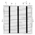
- FIG. 1 is a plan view illustrating an example of an appearance on the first surface side of a solar cell element according to an embodiment.
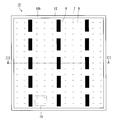
- FIG. 2 is a plan view showing an example of an appearance on the second surface side of the solar cell element according to the embodiment.
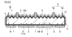
- FIG. 3 is a cross-sectional view showing an example of a cross section of the solar cell element taken along line III-III in FIGS.
- FIG. 4 is an enlarged plan view showing a portion IV in FIG.
- FIG. 5 is an enlarged cross-sectional view showing an example of a V portion in FIG.
- FIG. 6 is an enlarged cross-sectional view illustrating another example of the V portion in FIG. 3.
- FIG. 7A is a cross-sectional view showing, on an enlarged scale, a portion corresponding to the portion VII in FIG.
- FIG. 7B is an enlarged cross-sectional view of a portion corresponding to the VII portion of FIG. 5 for a passivation layer according to another modification.
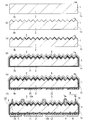
- FIG. 8A to FIG. 8F are end views for explaining a method for manufacturing a solar cell element according to an embodiment.
- a back electrode is formed by applying a conductive paste on a passivation layer formed on a silicon substrate and baking the conductive paste.
- a protective layer such as silicon nitride or silicon oxynitride is formed on the passivation layer so as to have a desired pattern by CVD or the like, and then a back electrode is formed on the protective layer.
- region which is not fired through by the electrically conductive paste in baking can be provided in a passivation layer, for example.
- the back electrode when the back electrode is formed or due to a temperature change in an actual use environment, the back electrode is expanded and cooled by heating. May cause contraction. For this reason, for example, the protective layer in contact with the back electrode may be peeled off from the passivation layer.
- the inventor of the present application has created a technique that can make it difficult to peel off the protective layer in the solar cell element, regardless of the temperature change in the actual use environment when the electrode is formed on the back side of the substrate.
- FIGS. 1 to 5 A solar cell element 10 according to an embodiment is shown in FIGS.
- the solar cell element 10 according to an embodiment is a PERC type solar cell element.
- the solar cell element 10 has a first surface 10a, a second surface 10b, and a side surface 10c.
- the first surface 10a is a light receiving surface on which light is mainly incident.
- the second surface 10b is a surface (also referred to as a back surface) located on the opposite side of the first surface 10a.
- the side surface 10c connects the first surface 10a and the second surface 10b.
- the solar cell element 10 includes a silicon substrate 1 as an example of a semiconductor substrate. Furthermore, the solar cell element 10 includes, for example, an antireflection layer 5, a first electrode 6, a second electrode 7, a third electrode 8, a fourth electrode 9, a passivation layer 11 and a passivation layer 11 as shown in FIGS. A protective layer 12 is provided.
- the silicon substrate 1 has a first surface 1a, a second surface 1b located on the opposite side of the first surface 1a, and a side surface 1c.
- the silicon substrate 1 includes a first semiconductor layer 2 that is a semiconductor region of one conductivity type (for example, p-type) and a reverse conductivity type (for example, n-type) that is positioned on the first surface 1a side of the first semiconductor layer 2.
- a second semiconductor layer 3 which is a semiconductor region of a type.
- the semiconductor substrate may be configured using a material other than silicon.
- a p-type silicon substrate can be used as the silicon substrate 1.
- the silicon substrate 1 may be a polycrystalline silicon or single crystal silicon substrate, for example.
- a substrate having a thickness of 250 ⁇ m or less and a thin substrate having a thickness of 150 ⁇ m or less can be used as the silicon substrate 1.
- the shapes of the first surface 1a and the second surface 1b of the silicon substrate 1 are not particularly limited. However, for example, when the silicon substrate 1 is viewed in plan, if the silicon substrate 1 has a substantially rectangular shape, a plurality of solar cell elements 10 can be arranged.
- the clearance gap between the solar cell elements 10 can be made small.
- the first semiconductor layer of the p-type semiconductor is obtained by adding an impurity such as boron or gallium as a dopant element to the silicon substrate 1. 2 can be produced.
- the second semiconductor layer 3 is located on the first semiconductor layer 2, for example. Specifically, for example, the second semiconductor layer 3 is located on the first surface 1 a side of the first semiconductor layer 2. In this case, the first semiconductor layer 2 and the second semiconductor layer 3 are stacked.
- the second semiconductor layer 3 has a conductivity type opposite to that of the first semiconductor layer 2 (p-type in one embodiment) (n-type in one embodiment).
- the silicon substrate 1 has a pn junction at the interface between the first semiconductor layer 2 and the second semiconductor layer 3, for example.
- the second semiconductor layer 3 can be formed, for example, by introducing an impurity such as phosphorus into the surface layer portion on the first surface 1a side of the silicon substrate 1 by diffusion or the like.
- the first surface 1a of the silicon substrate 1 may have a fine concavo-convex structure (also referred to as a texture) for reducing the reflectance of irradiated light, as shown in FIG. 3, for example.
- the height of the convex portion of the texture is, for example, about 0.1 ⁇ m to 10 ⁇ m.
- the length between the tops of adjacent convex portions of the texture is, for example, about 0.1 ⁇ m to 20 ⁇ m.
- the concave portion may have a substantially spherical shape, or the convex portion may have a pyramid shape.
- the “height of the convex portion” described above is the texture from the reference line in a direction perpendicular to the reference line. It means the distance to the top of the convex part.
- the silicon substrate 1 has, for example, a third semiconductor layer 4.
- the third semiconductor layer 4 is located on the second surface 1b side of the silicon substrate 1, for example.
- the conductivity type of the third semiconductor layer 4 the same conductivity type as the first semiconductor layer 2 (p-type in one embodiment) is employed.
- the concentration of the dopant contained in the third semiconductor layer 4 is higher than the concentration of the dopant contained in the first semiconductor layer 2. That is, in the third semiconductor layer 4, for example, a dopant element having a concentration higher than the concentration of the dopant element doped to make one conductivity type in the first semiconductor layer 2 exists.
- the third semiconductor layer 4 functions as a BSF layer (Back Surface Field) capable of forming an internal electric field on the second surface 1b side of the silicon substrate 1.
- BSF layer Back Surface Field
- the third semiconductor layer 4 can be formed, for example, by introducing a dopant element such as boron or aluminum into the surface layer portion on the second surface 1b side of the silicon substrate 1 by diffusion.
- the concentration of the dopant element contained in the first semiconductor layer 2 is set to about 5 ⁇ 10 15 atoms / cm 3 to 1 ⁇ 10 17 atoms / cm 3
- the third semiconductor layer 4 contains The concentration of the dopant element is about 1 ⁇ 10 18 atoms / cm 3 to about 5 ⁇ 10 21 atoms / cm 3
- the third semiconductor layer 4 may exist at a contact portion between a second electrode 7 and a silicon substrate 1 described later.
- the antireflection layer 5 can reduce the reflectance of the light irradiated to the 1st surface 10a of the solar cell element 10, for example.
- a material of the antireflection layer 5 for example, a silicon oxide, aluminum oxide, or silicon nitride layer is employed.
- the refractive index and thickness of the antireflection layer 5 for example, a refraction that can realize low reflection conditions for light in a wavelength range that can be absorbed by the silicon substrate 1 and contribute to power generation in sunlight. Rate and thickness can be employed as appropriate.
- the antireflection layer 5 can have a refractive index of about 1.8 to 2.5 and a thickness of about 20 nm to 120 nm.
- the first electrode 6 is an electrode for collecting electricity generated by the silicon substrate 1 on the second surface 1b side of the silicon substrate 1, as shown in FIGS.
- the first electrode 6 is located on the protective layer 12, for example.
- the first electrode 6 is positioned so as to be electrically connected to the second electrode 7 and the third electrode 8, for example.
- at least a part of the third electrode 8 may be connected to the first electrode 6.
- the thickness of the first electrode 6 is, for example, about 15 ⁇ m to 50 ⁇ m.
- the first electrode 6 includes, for example, aluminum as a main component.
- the first electrode 6 can be formed by, for example, applying a metal paste containing aluminum as a main component in a desired shape and then firing the metal paste.
- “main component” means that the ratio of the total component is 50% or more.
- the second electrode 7 is located on the second surface 1 b side of the silicon substrate 1 so as to penetrate the passivation layer 11 and the protective layer 12.
- the 2nd electrode 7 is located so that the silicon substrate 1 and the 1st electrode 6 may be connected, for example.
- the 2nd electrode 7 is connected with the 3rd semiconductor layer 4 located in the part by the side of the 2nd surface 1b of the silicon substrate 1.
- the 2nd electrode 7 is located in the 2nd surface 1b side of the silicon substrate 1 with a fixed space
- the shortest distance between the centers of the adjacent second electrodes 7 is An (however, the subscript n Is a positive integer, and so on.
- the shortest length of the second electrode 7 is, for example, a dot (dot) shape when the second electrode 7 is seen through from the second surface 10b side.
- the second electrode 7 includes, for example, aluminum as a main component.
- the second electrode 7 can be formed by, for example, applying a metal paste containing aluminum as a main component in a desired shape and then firing the metal paste.
- the first electrode 6 and the second electrode 7 may be formed at the same time using, for example, the same metal paste mainly composed of aluminum.
- the third electrode 8 is located on the second surface 1b side of the silicon substrate 1, for example, as shown in FIGS.
- the 3rd electrode 8 is an electrode for taking out the electricity obtained by power generation by solar cell element 10 outside, for example.
- the thickness of the third electrode 8 is about 10 ⁇ m to 30 ⁇ m.
- the width of the third electrode 8 is about 1.3 mm to 7 mm.
- the third electrode 8 includes, for example, silver as a main component.
- the third electrode 8 can be formed, for example, by applying a metal paste containing silver as a main component to a desired shape by screen printing or the like and then baking the metal paste.
- the 4th electrode 9 is an electrode located in the 1st surface 1a side of silicon substrate 1, for example.
- the fourth electrode 9 includes, for example, an output extraction electrode 9 a and a plurality of linear current collection electrodes 9 b.
- the output extraction electrode 9a is, for example, an electrode for extracting electricity obtained by power generation to the outside.
- the length of the output extraction electrode 9a in the short direction (hereinafter also referred to as the width) is, for example, about 1.3 mm to 2.5 mm.
- the output extraction electrode 9a intersects with the collector electrode 9b.
- the current collecting electrode 9b is an electrode for collecting electricity generated from the silicon substrate 1, for example.
- each collecting electrode 9b is, for example, about 50 ⁇ m to 200 ⁇ m. In this case, the width of the collector electrode 9b is smaller than the width of the output extraction electrode 9a.
- the plurality of linear current collecting electrodes 9b are positioned so as to have an interval of about 1 mm to 3 mm, for example.
- the thickness of the fourth electrode 9 is, for example, about 10 ⁇ m to 40 ⁇ m.
- the 4th electrode 9 contains silver as a main component, for example.
- the fourth electrode 9 can be formed, for example, by applying a metal paste containing silver as a main component to a desired shape by screen printing or the like and then baking the metal paste.
- the auxiliary electrode 9c having the same shape as the current collecting electrode 9b may be positioned on the peripheral edge of the silicon substrate 1 so as to electrically connect the current collecting electrodes 9b.
- the passivation layer 11 is located on at least the second surface 1b of the silicon substrate 1, for example.
- the passivation layer 11 can reduce minority carrier recombination when, for example, photoelectric conversion is performed in response to sunlight irradiation.
- the thickness of the passivation layer 11 is, for example, about 10 nm to 200 nm.
- the protective layer 12 is positioned, for example, so as to have a desired pattern on the passivation layer 11. In this pattern, for example, when the protective layer 12 is seen through from the second surface 10b side, a region in which the protective layer 12 is not present in a region where the plurality of second electrodes 7 are formed (also referred to as a non-formed region). ) Is located.
- the shape of the non-formation region seen through the plane may be, for example, a dot (dot) shape or a band (line) shape.
- the pitch of the non-formation regions (corresponding to the shortest distance An between the centers of the adjacent second electrodes) is, for example, about 0.3 mm to 3 mm.
- the diameter or width (corresponding to the shortest length Cn of the second electrode) of the non-formation region may be, for example, about 10 ⁇ m to 500 ⁇ m. If such a pitch and diameter or width of the non-formation region is adopted, for example, good current collection efficiency by the plurality of second electrodes 7 and good electric field passivation effect by the passivation layer 11 are realized in a balanced manner. Is done. As a result, good photoelectric conversion efficiency in the solar cell element 10 can be realized.
- the metal paste is baked.
- the metal paste applied on the non-formation region of the passivation layer 11 fires through the passivation layer 11 during firing and is electrically connected to the silicon substrate 1.
- the third semiconductor layer 4 which is a BSF layer may be formed on the silicon substrate 1.
- the region covered with the protective layer 12 is not fired through with the metal paste. For this reason, the electric field passivation effect by the passivation layer 11 is not easily lowered.
- the second electrode 7 is positioned so as to be in contact with the third semiconductor layer 4 existing in the surface layer portion of the silicon substrate 1 while penetrating the passivation layer 11 and the protective layer 12.
- the second electrode 7 is electrically connected to the first electrode 6. Thereby, the 2nd electrode 7 can take out the electricity from the silicon substrate 1 efficiently.
- the thickness of the protective layer 12 is, for example, about 0.5 ⁇ m to 10 ⁇ m.
- the thickness of the protective layer 12 includes, for example, the type of component included in the insulating paste described later or the content of the component, the size of the uneven shape of the second surface 1b of the silicon substrate 1, and the metal paste.
- the glass frit is appropriately changed depending on the kind of glass frit or the content of the glass frit and the firing conditions when the first electrode 6 is formed.
- the protective layer 12 can be formed, for example, by applying an insulating paste described later by a screen printing method or the like and then drying the insulating paste. For example, as shown in FIG.
- the protective layer 12 may further include a non-formed region where the protective layer 12 does not exist in the region where the third electrode 8 is formed.
- the third electrode 8 is directly connected to the silicon substrate 1. Thereby, the joint strength of the third electrode 8 to the silicon substrate 1 can be increased. In other words, for example, the third electrode 8 is difficult to peel off.
- the insulating paste for example, a paste containing a siloxane resin, an organic solvent, and a plurality of fillers is employed.
- the siloxane resin is a siloxane compound having a Si—O—Si bond.
- the siloxane resin may be a low molecular weight resin having a molecular weight of 10,000 or less, which is generated by hydrolyzing alkoxysilane or silazane or the like and performing condensation polymerization.
- the insulating paste can be generated as follows, for example.
- a siloxane resin precursor, water, an organic solvent, and a catalyst are mixed in a container and stirred to produce a mixed solution.
- a silane compound containing a Si—O bond or a silazane compound containing a Si—N bond which has the property of becoming a siloxane resin by hydrolysis and condensation polymerization
- Water is a liquid for hydrolyzing the precursor of the siloxane resin.
- the organic solvent is a solvent for producing a paste containing a siloxane resin from a siloxane resin precursor.
- the catalyst can control the reaction rate when the siloxane resin precursor undergoes hydrolysis and condensation polymerization.
- the catalyst for example, one or more inorganic acids or one or more organic acids of hydrochloric acid, nitric acid, sulfuric acid, boric acid, phosphoric acid, hydrofluoric acid, and acetic acid are used.
- one or more inorganic bases or one or more organic bases among ammonia, sodium hydroxide, potassium hydroxide, barium hydroxide, calcium hydroxide, pyridine and the like may be used.
- the catalyst may be, for example, a combination of an inorganic acid and an organic acid, or a combination of an inorganic base and an organic base.
- by-products including alcohol and water generated by hydrolysis during the production of the mixed solution are removed from the mixed solution by evaporating by heating in a temperature range from room temperature to about 90 ° C., for example.
- the by-product may not be removed from the mixed solution.
- a filler containing silicon oxide, aluminum oxide, titanium oxide or the like is added to the mixed solution from which the by-products have been removed.
- the mixed solution may be stirred.
- a filler may be mixed when a siloxane resin precursor, water, an organic solvent, and a catalyst are mixed in a container.
- the viscosity of the mixed solution is stabilized by storing the mixed solution at room temperature. Thereby, an insulating paste is generated.
- the protective layer 12 may be formed on the passivation layer 11 by using a dry process such as PECVD (plasma-enhanced chemical vapor deposition) method using a mask.
- PECVD plasma-enhanced chemical vapor deposition
- the protective layer 12 contains, for example, silicon oxide as a main component.
- silicon oxide since the thermal expansion coefficient of silicon oxide is close to 1, the tensile or shrinkage stress due to temperature change is reduced between the passivation layer 11 and the protective layer 12. Thereby, for example, stress generated at the interface between the passivation layer 11 and the protective layer 12 can be reduced. As a result, for example, peeling at the interface between the protective layer 12 and the passivation layer 11 is less likely to occur.
- the passivation layer 11 includes aluminum oxide
- the electric field passivation effect in the passivation layer 11 is unlikely to decrease.
- the density of positive fixed charges in silicon oxide tends to be about 1 to 2 orders of magnitude smaller than the density of negative fixed charges in aluminum oxide.
- the density of negative fixed charges in aluminum oxide tends to be about 1 ⁇ 10 11 / cm 2 to 1 ⁇ 10 13 / cm 2
- the density of positive fixed charges in silicon oxide is 6 ⁇ It tends to be about 10 10 / cm 2 .
- the density of positive fixed charges in silicon nitride is about 1 ⁇ 10 12 / cm 2, which is larger than that of silicon oxide.
- the protective layer 12 includes silicon oxide, the electric field passivation effect in the passivation layer 11 is less likely to decrease than when the protective layer 12 includes silicon nitride.
- the protective layer 12 may have, for example, an alkyl group such as a methyl group (CH 3 ) or an ethyl group (C 2 H 5 ) inside.
- an alkyl group such as a methyl group (CH 3 ) or an ethyl group (C 2 H 5 ) inside.
- the protective layer 12 when the protective layer 12 includes an alkyl group, electric charges are reduced on the surface of the protective layer 12 mainly composed of silicon oxide. For this reason, the protective layer 12 has water repellency and water molecules do not easily pass through the protective layer 12. Thereby, not only is it excellent in reliability such as moisture resistance, but also the solar cell element 10 that makes it difficult for the protective layer 12 and the passivation layer 11 to peel off due to the permeation of water molecules can be realized.
- the fact that the protective layer 12 contains an alkyl group can be confirmed, for example, by time-of-flight secondary ion mass spectrometry (TOF-SIMS).
- the protective layer 12 containing an alkyl group can be realized, for example, by forming the protective layer 12 using the above-described insulating paste.
- the protective layer 12 may be located not only on the passivation layer 11 located on the second surface 1b side of the silicon substrate 1, but also on the side surface 10c of the solar cell element 10, for example, You may be located on the antireflection layer 5 located on the outer peripheral part of 10a. In this case, for example, the leakage current of the solar cell element 10 can be reduced due to the presence of the protective layer 12.
- the protective layer 12 has at least one gap portion 13.
- the gap 13 is formed from a surface (also referred to as a first lower surface) Bf1 of the first electrode 6 on the silicon substrate 1 side to a surface (first upper surface) of the passivation layer 11 on the first lower surface Bf1 side. It is also located up to Uf1.
- the protective layer 12 is partially pulled due to the presence of the gap portion 13. Or shrink. For this reason, for example, the protective layer 12 is hardly peeled off from the passivation layer 11.
- the protective layer 12 has a plurality of gaps 13.
- the cross section of the protective layer 12 having the gap 13 can be confirmed using, for example, a scanning electron microscope (SEM: Scanning Electron Microscope) or a transmission electron microscope (TEM: Transmission Electron Microscope).
- the solar cell element 10 is divided by laser light irradiation or the like, a part of the divided solar cell element 10 is embedded in an epoxy resin or the like as a sample, and the resin is solidified. By polishing, a cross section of the protective layer 12 for observation can be prepared. Further, for example, the state in which the gap portion 13 is viewed in plan can be confirmed using an SEM or an optical microscope after removing the first electrode 6 using hydrochloric acid for the solar cell element 10.
- the gap 13 may have a linear opening.
- the gap 13 may have a linear opening on the surface (also referred to as a second upper surface) Uf2 of the protective layer 12 on the first electrode 6 side.
- the gap 13 has a linear opening along a thin line drawn with a two-dot chain line.
- a plurality of gaps 13 are located between a plurality of adjacent second electrodes 7.
- the protective layer 12 is more partially pulled or contracted than when 13 is formed in a dot shape. Thereby, for example, peeling of the protective layer 12 from the passivation layer 11 is further less likely to occur.
- the distance between the centers of the adjacent gaps 13 of the plurality of gaps 13 on the second upper surface Uf ⁇ b> 2 on the first electrode 6 side of the protective layer 12 is the adjacent of the plurality of second electrodes 7. It is smaller than the shortest distance An between the centers of the matching second electrodes.
- the distance between the centers of the adjacent gaps 13 is, for example, 200 ⁇ m or less.
- the plurality of gaps 13 having such center-to-center distances are formed by, for example, applying the insulating paste on the passivation layer 11 and drying the first electrode 6 applied on the dried insulating paste. It can be formed when the metal paste for forming is fired. As the heating temperature at the time of firing, for example, about 600 ° C. to 850 ° C. can be adopted.
- the distance between the centers of the adjacent gaps 13 is the above, for example, when a tensile or contracting force is applied from the first electrode 6 to the protective layer 12 due to a temperature change of the solar cell element 10, the protective layer 12 is more It is partially pulled or shrunk. For this reason, for example, peeling of the protective layer 12 from the passivation layer 11 is further less likely to occur.
- the distance between the centers of the adjacent gaps 13 (hereinafter also referred to as the distance between the centers of the gaps) is indicated by Bn as shown in FIG.
- the distance Bn between the centers of the adjacent voids is, for example, the distance between the adjacent voids when the protective layer 12 is viewed in plan with an SEM or an optical microscope, or when the cross section of the protective layer 12 is observed with the SEM or TEM. Any distance between the centers may be used.
- the opening width of the gap 13 in the second upper surface Uf2 on the first electrode 6 side of the protective layer 12 may be smaller than the shortest length Cn of the second electrode.
- the opening width of the gap 13 is, for example, 2 ⁇ m or less.
- the diameter of the aluminum particles contained in the metal paste for forming the second electrode 7 is smaller than the shortest length Cn of the second electrode and larger than the opening width of the gap 13, the protection is achieved.
- aluminum particles are unlikely to enter the gap 13.
- the area where the passivation layer 11 is fired through with the metal paste through the gap 13 is reduced.
- the electric field passivation effect is unlikely to decrease.
- the opening width of the gap 13 is within the above range, an excessive decrease in the contact area between the first electrode 6 and the protective layer 12 is reduced. Thereby, for example, the first electrode 6 is difficult to peel from the protective layer 12.
- the opening width of each of the plurality of gaps 13 (hereinafter also referred to as the opening width of the gaps) is indicated by Dn.
- the width of the plurality of gaps 13 decreases from the lower surface (first lower surface) Bf1 of the first electrode 6 toward the upper surface (first upper surface) Uf1 of the passivation layer 11. Also good.
- the width of the gap 13 may be, for example, the length in the short direction of the gap 13 along the second surface 1 b of the silicon substrate 1. If such a structure is adopted, for example, the contact area between the first electrode 6 and the protective layer 12 is reduced, so that the tensile stress and / or the contraction stress applied to the protective layer 12 is reduced. On the other hand, for example, the contact area between the protective layer 12 and the passivation layer 11 is larger than the contact area between the first electrode 6 and the protective layer 12.
- the protective layer 12 becomes difficult to peel from the passivation layer 11.
- the widths of the plurality of gaps 13 become smaller from the first lower surface Bf ⁇ b> 1 of the first electrode 6 toward the first upper surface Uf ⁇ b> 1 of the passivation layer 11,
- the distance Bn between the centers of the matching gaps and the opening width Dn of the gaps are determined based on the gaps 13 on the first electrode 6 side.
- the passivation layer 11 is a second passivation layer containing silicon oxide (oxidized oxide) located between the first passivation layer 11 a containing aluminum oxide and the protective layer 12. (Also referred to as a silicon layer) 11b.
- the second passivation layer 11b can be formed by, for example, an ALD method.
- the protective layer 12 includes silicon oxide, for example, the second passivation layer 11b is connected to the protective layer 12 and the first layer. It functions as a buffer layer between the passivation layer 11a.
- the silicon oxide constituting the second passivation layer 11 b is the same as the silicon oxide constituting the protective layer 12. For this reason, the adhesion between the protective layer 12 and the passivation layer 11 is improved.
- the thickness of the second passivation layer 11b may be about 5 nm to 15 nm, for example. If the thickness of the second passivation layer 11b is within the above range, for example, even if there is an influence of the positive fixed charge of the second passivation layer 11b, the electric field passivation effect due to the negative fixed charge of the first passivation layer 11a is obtained. It is hard to decline. For example, if the thickness of the second passivation layer 11b is smaller than the thickness of the first passivation layer 11a, the electric field passivation effect due to the negative fixed charge of the first passivation layer 11a is unlikely to decrease.
- the second passivation layer 11b when the second passivation layer 11b is formed by an ALD method using a silicon raw material such as bisdiethylaminosilane (BDEAS), carbon and hydrogen are contained in the second passivation layer 11b containing silicon oxide. May be contained. Carbon and hydrogen contained in the second passivation layer 11b can be detected, for example, by measurement using TOF-SIMS.
- the second passivation layer 11b unlike the protective layer 12, the second passivation layer 11b is unlikely to contain an alkyl group such as a methyl group (CH 3 ) or an ethyl group (C 2 H 5 ).
- the second passivation layer 11b is likely to contain a small amount of nitrogen contained in the source gas used in the ALD method, for example.
- the passivation layer 11 is provided between the first semiconductor layer 2 (p-type semiconductor region in one embodiment) and the first passivation layer 11a containing aluminum oxide.
- a third passivation layer (also referred to as a silicon oxide layer) 11c containing silicon oxide may be provided.
- the third passivation layer 11c functions as a buffer layer between the silicon substrate 1 and the first passivation layer 11a.
- the adhesion between the silicon substrate 1 and the passivation layer 11 is improved.
- the thickness of the third passivation layer 11c may be about 0.1 nm to 1 nm, for example.
- the thickness of the third passivation layer 11c containing silicon oxide is within the above range, for example, even if the third passivation layer 11c has a positive fixed charge, the first passivation layer 11c is present due to the presence of the third passivation layer 11c.
- the electric field passivation effect by the passivation layer 11a is not easily lowered.
- the thickness of the third passivation layer 11c is smaller than both the thickness of the first passivation layer 11a and the second passivation layer 11b, the electric field passivation effect by the first passivation layer 11a is unlikely to decrease.
- the total thickness of the second passivation layer 11b and the third passivation layer 11c may be smaller than the thickness of the first passivation layer 11a.
- the second passivation layer 11b and the third passivation layer 11c can be formed without irradiating the silicon substrate 1 or the first passivation layer 11a with plasma, for example, by using an ALD method or the like.
- plasma damage is unlikely to occur in the silicon substrate 1 and / or the first passivation layer 11a.
- plasma damage is damage caused by etching of the silicon substrate 1 and / or the first passivation layer 11a due to collision of electrons generated in the plasma.
- plasma damage is damage caused by etching of the silicon substrate 1 and / or the first passivation layer 11a due to collision of electrons generated in the plasma.
- defects are generated or impurities are mixed.
- the gap portion 13 for example, a structure that does not include the electrode component of the first electrode 6 inside is employed.
- This structure may be a structure in which the center of the metal particle of the first electrode 6 is not located inside the gap portion 13 when the cross section of the protective layer 12 is observed using, for example, SEM or TEM. If such a configuration is adopted, for example, the portion of the passivation layer 11 facing the gap portion 13 is not fire-through, and the gap portion 13 of the second surface 1b of the silicon substrate 1 is not exposed.
- the third semiconductor layer 4 is not formed around the facing surface layer portion.
- the shape of the linear opening of the gap portion 13 may be, for example, a linear shape or a curved shape including a wave shape.
- the distance Bn between the centers of the gaps on the second surface 1b of the protective layer 12 may be equal to or greater than the shortest distance An between the centers of the adjacent second electrodes.
- the insulating paste is printed a plurality of times with the interval between the regions where the thickness of the insulating paste is locally increased being equal to or greater than the shortest distance An between the centers of the second electrodes. Good.
- the shape of the opening of the gap 13 in the second upper surface Uf2 of the protective layer 12 is not limited to a linear shape, and may be a dotted shape.
- the thickness of the insulating paste can be locally increased by printing the insulating paste in a dotted pattern a plurality of times on the portion of the passivation layer 11 where the void 13 is to be formed. it can.
- the protective layer 12 is likely to crack.
- the cracks generated at this time can serve as the gap 13.
- the protective layer 12 is formed so that the thickness in the region where the gap 13 is formed is 1.3 to 1.5 times the thickness in the region where the gap 13 is not formed. Just do it.
- the thickness of the protective layer 12 may be appropriately changed according to the material of the insulating paste, for example.
- the solar cell element 10 is not a PERC type solar cell element, but is a back contact type having a structure such as IBC (Interdigitated Back Contact), MWT (Metal Wrap Through) and EWT (Emitter Wrap Through). It may be a solar cell element.
- the solar cell element 10 should just have the structure where the passivation layer, the protective layer, and the electrode are laminated
- a silicon substrate 1 is prepared.
- the silicon substrate 1 is formed by, for example, an existing CZ (Czochralski) method or a casting method.
- CZ Czochralski
- a casting method an example in which a p-type polycrystalline silicon substrate is used as the silicon substrate 1 will be described.
- an ingot of polycrystalline silicon is produced by a casting method.
- the ingot is sliced to a thickness of, for example, 250 ⁇ m or less to produce the silicon substrate 1.
- the surface of the silicon substrate 1 may be etched by a very small amount with an aqueous solution such as NaOH, KOH, hydrofluoric acid, or hydrofluoric acid. .
- a texture is formed on the first surface 1 a of the silicon substrate 1.
- a method for forming the texture for example, wet etching using an alkaline solution containing NaOH or the like, or an acid solution such as hydrofluoric acid, or dry etching using a RIE (Reactive Ion Etching) method or the like can be used.
- Such a second semiconductor layer 3 can be formed using, for example, a coating thermal diffusion method or a vapor phase thermal diffusion method.
- the coating thermal diffusion method may be a method in which, for example, paste-like phosphorous pentoxide (P 2 O 5 ) is applied to the surface of the silicon substrate 1 and phosphorus is thermally diffused on the surface layer portion of the silicon substrate 1.
- the vapor phase thermal diffusion method may be any method that uses gaseous phosphorus oxychloride (POCl 3 ) as a diffusion source, for example.
- the second semiconductor layer 3 may be formed to have a depth of about 0.1 ⁇ m to 2 ⁇ m and a sheet resistance value of about 40 ⁇ / ⁇ to 200 ⁇ / ⁇ .
- the silicon substrate 1 is subjected to a heat treatment for about 5 minutes to 30 minutes at a temperature of about 600 ° C. to 800 ° C. in an atmosphere having a diffusion gas containing POCl 3 or the like.
- Phosphorus glass is formed on the first surface 1a of the silicon substrate 1.
- the silicon substrate 1 is subjected to heat treatment for about 10 minutes to 40 minutes at a high temperature of about 800 ° C. to 900 ° C. in an atmosphere of an inert gas such as argon or nitrogen.
- an inert gas such as argon or nitrogen.
- the second semiconductor layer 3 is formed on the second surface 1b side of the silicon substrate 1.
- the formed second semiconductor layer 3 is removed by etching.
- the p-type semiconductor region is exposed on the second surface 1b side of the silicon substrate 1.
- the second semiconductor layer 3 formed on the second surface 1b side of the silicon substrate 1 is removed by immersing only the second surface 1b side of the silicon substrate 1 in a hydrofluoric acid solution. Thereafter, the phosphorus glass adhering to the first surface 1a side of the silicon substrate 1 when the second semiconductor layer 3 is formed is removed by etching.
- the phosphorous glass remains on the first surface 1a side, and the second semiconductor layer 3 formed on the second surface 1b side of the silicon substrate 1 is removed by etching, whereby the first surface of the silicon substrate 1 is removed.
- the second semiconductor layer 3 on the 1a side is not easily removed or damaged.
- the second semiconductor layer 3 formed on the side surface 1c of the silicon substrate 1 may also be removed.
- a diffusion mask is formed in advance on the second surface 1b side, the second semiconductor layer 3 is formed by vapor phase thermal diffusion, etc., and then the diffusion mask is removed. May be.
- a structure similar to that described above can also be formed by such a process.
- the second semiconductor layer 3 can be prevented from being formed on the second surface 1b side of the silicon substrate 1. Thereby, the process of removing the 2nd semiconductor layer 3 by the side of the 2nd surface 1b becomes unnecessary.
- a passivation layer 11 is formed on the first surface 1 a of the first semiconductor layer 2 and the second surface 1 b of the second semiconductor layer 3.
- the passivation layer 11 As a method for forming the passivation layer 11, for example, an ALD method can be used. Thereby, the passivation layer 11 can be formed all around the side surface 1c of the silicon substrate 1.
- the ALD method for example, first, the silicon substrate 1 on which the second semiconductor layer 3 is formed is placed in a chamber of a film forming apparatus. For example, in a state where the silicon substrate 1 is heated from 100 ° C. to 250 ° C., a series of processes including the process A to the process D shown below are repeated a plurality of times. Thereby, the passivation layer 11 (or the first passivation layer 11a) mainly composed of aluminum oxide having a desired thickness can be formed.
- An example of the contents of Step A to Step D is as follows.
- a silicon raw material such as bisdiethylaminosilane (BDEAS) for forming a silicon oxide layer or an aluminum raw material such as trimethylaluminum (TMA) for forming an aluminum oxide layer is formed by using argon (Ar ) Along with a carrier gas such as gas or nitrogen gas, the silicon substrate 1 is supplied. Thereby, the silicon raw material or the aluminum raw material is adsorbed on the entire periphery of the silicon substrate 1.
- the time during which BDEAS or TMA is supplied onto the silicon substrate 1 may be, for example, about 15 milliseconds to 3000 milliseconds.
- the surface of the silicon substrate 1 may be terminated with an OH group. That is, the surface of the silicon substrate 1 may have a Si—O—H structure.
- This structure can be formed, for example, by treating the silicon substrate 1 with dilute hydrofluoric acid and then washing with pure water.
- Step B The inside of the chamber of the film forming apparatus is cleaned with nitrogen gas. At this time, the silicon material or aluminum material in the chamber is removed. At this time, the silicon raw material or aluminum raw material other than the component chemically adsorbed on the silicon substrate 1 at the atomic layer level is removed from the silicon raw material or aluminum raw material physically and chemically adsorbed on the silicon substrate 1.
- the time for purifying the inside of the chamber with nitrogen gas may be about 1 second to several tens of seconds, for example.
- Step C An oxidizing agent such as water or ozone gas is supplied into the chamber of the film forming apparatus. At this time, the alkyl group contained in BDEAS or TMA is removed and replaced with an OH group. Thereby, an atomic layer of silicon oxide or aluminum oxide is formed on the silicon substrate 1.
- the time for supplying the oxidizing agent into the chamber may be about 750 milliseconds to 1100 milliseconds, for example.
- hydrogen atoms (H) are supplied into the chamber together with the oxidizing agent, so that hydrogen atoms are more easily contained in silicon oxide or aluminum oxide.
- Step D The inside of the chamber of the film forming apparatus is cleaned with nitrogen gas. Thereby, the oxidizing agent in the chamber is removed. At this time, for example, an oxidant that has not contributed to the reaction during the formation of atomic layer level silicon oxide or aluminum oxide on the silicon substrate 1 is removed.
- the time for purifying the inside of the chamber with nitrogen gas may be, for example, about 1 second to several tens of seconds.
- the second passivation layer 11b containing silicon oxide may be formed between the protective layer 12 and the first passivation layer 11a containing aluminum oxide by the ALD method.
- the third passivation layer 11c may be formed between the first semiconductor layer 2 and the first passivation layer 11a containing aluminum oxide.
- the silicon substrate 1 is heated to the same temperature range as described above, and the series of steps including the step A to the step D is repeated a plurality of times, so that each of the silicon oxides containing the silicon oxide is obtained.
- a second passivation layer 11b and / or a third passivation layer 11c can be formed.
- the antireflection layer 5 is formed on the passivation layer 11 formed on the first surface 1 a of the first semiconductor layer 2.
- the antireflection layer 5 can be formed using PECVD or sputtering.
- the silicon substrate 1 may be heated in advance to a temperature higher than the temperature at which the passivation layer 11 is formed. Thereafter, a mixed gas containing silane (SiH 4 ) and ammonia (NH 3 ) is diluted with nitrogen (N 2 ) and decomposed by glow discharge at a reaction pressure in the range of 50 Pa to 200 Pa. At this time, for example, silane and ammonia are turned into plasma and deposited on the heated silicon substrate 1.
- the antireflection layer 5 can be formed on the passivation layer 11 on the first surface 1 a of the silicon substrate 1.
- the film formation temperature of the antireflection layer 5 is set to about 350 ° C. to 650 ° C.
- the temperature for preheating the silicon substrate 1 is about 400 ° C. to 700 ° C., which is about 50 ° C. higher than the film formation temperature. can do.
- a frequency of the high-frequency power source necessary for glow discharge for example, a frequency of 10 kHz to 500 kHz can be used.
- the flow rate of the mixed gas is appropriately determined depending on the size of the reaction chamber, for example.
- the flow rate of the mixed gas may be in the range of 150 ml / min (sccm) to 6000 ml / min (sccm).
- a protective layer 12 is formed on at least a part of the passivation layer 11.
- an insulating paste containing silicon oxide is applied to at least a part of the passivation layer 11 using a screen printing method or the like so as to form a desired pattern.
- the insulating paste is dried using a hot plate or a drying furnace under drying conditions where the maximum temperature is about 150 ° C. to 350 ° C. and the heating time is about 1 minute to 10 minutes.
- the protective layer 12 having a desired pattern can be formed on the passivation layer 11 (or the first passivation layer 11a).
- the passivation layer 11 is fired with a metal paste for forming the first electrode 6 when the first electrode 6 described later is formed. It becomes difficult to be passed through. As a result, for example, the passivation effect is difficult to be reduced. In addition, for example, the adhesion between the protective layer 12, the passivation layer 11 (or the first passivation layer 11 a), and the first electrode 6 is difficult to be reduced.
- the protective layer 12 may be formed at a position other than the position where the second electrode 7 is in contact with the second surface 1b of the silicon substrate 1, for example. In this case, for example, even if the insulating paste is printed in a desired pattern so that the non-formation region of the protective layer 12 is formed in the region where the plurality of second electrodes 7 are formed on the passivation layer 11. Good. At this time, for example, a step of removing a part of the protective layer 12 by laser beam irradiation or the like becomes unnecessary. As a result, for example, the productivity of the solar cell element 10 can be improved.
- the gap portion 13 is likely to be formed at a position where the insulating paste is applied so that the film thickness is thicker than the surrounding portion.
- the thickness of the insulating paste can be locally increased by printing the insulating paste a plurality of times on the portion of the passivation layer 11 where the gap 13 is to be formed.
- the protective layer 12 formed after drying the insulating paste has a thickness distribution. Then, when cooling in the step of baking the metal paste (also referred to as a baking step), the maximum temperature described later is 600 ° C. to 850 ° C., the portion of the protective layer 12 where the thickness is large is the portion where the thickness is small Shrinkage is more likely to occur.
- the protective layer 12 is likely to crack.
- the cracks generated at this time can serve as the gap 13.
- the protective layer 12 is formed so that the thickness in the region where the gap 13 is formed is 1.3 to 1.5 times the thickness in the region where the gap 13 is not formed. Just do it.
- the thickness of the protective layer 12 may be appropriately changed according to the material of the insulating paste, for example.
- the thickness of the protective layer 12 may be appropriately changed according to the material of the insulating paste, for example.
- the thickness of the protective layer 12 may be appropriately changed according to the material of the insulating paste, for example.
- the application amount of the insulating paste on the passivation layer 11 is, for example, the size of the concavo-convex shape on the second surface 1b of the silicon substrate 1, the kind of glass frit contained in the metal paste mainly composed of aluminum described later, or What is necessary is just to change suitably according to content and the baking conditions at the time of formation of the 2nd electrode 7.
- FIG. 1 the size of the concavo-convex shape on the second surface 1b of the silicon substrate 1, the kind of glass frit contained in the metal paste mainly composed of aluminum described later, or What is necessary is just to change suitably according to content and the baking conditions at the time of formation of the 2nd electrode 7.
- the first electrode 6, the second electrode 7, the third electrode 8, and the fourth electrode 9 are formed as follows.
- the first electrode 6 is formed using, for example, a metal paste (also referred to as a first metal paste) containing metal powder containing aluminum as a main component, an organic vehicle, glass frit, and the like.
- a metal paste also referred to as a first metal paste
- the first metal paste is applied to the second surface 1b side of the silicon substrate 1 so as to come into contact with a part of the second metal paste after application described later.
- the first metal paste may be applied to almost the entire surface on the second surface 1b side of the silicon substrate 1 except for a part of the portion where the third electrode 8 is formed.
- a coating method of the first metal paste for example, a screen printing method or the like can be used.
- the first metal paste may be dried by evaporating the solvent at a predetermined temperature. Thereafter, for example, the first electrode is baked in a firing furnace under conditions where the maximum temperature is about 600 ° C. to 850 ° C. and the heating time is about several tens of seconds to several tens of minutes. 6 may be formed on the second surface 1b side of the silicon substrate 1.
- the first metal paste located on the protective layer 12 is blocked by the protective layer 12, so that the fire-through of the passivation layer 11 is unlikely to occur. That is, for example, due to the presence of the protective layer 12, the fire through of the passivation layer 11 is hardly affected when the first metal paste is fired. In other words, for example, a reduction in the electric field passivation effect due to a decrease in the passivation layer 11 or the like hardly occurs.
- the second electrode 7 is connected to the first semiconductor layer 2 so that the first metal paste fires through the passivation layer 11 and penetrates the region where the protective layer 12 is not formed. It is formed in such a form.
- the aluminum contained in the first metal paste fired through the passivation layer 11 diffuses into the surface layer portion of the second surface 1 b of the silicon substrate 1, thereby forming the third semiconductor layer 4. Is done.
- the third electrode 8 is formed, for example, using a metal paste (also referred to as a second metal paste) containing a metal powder containing silver as a main component, an organic vehicle, glass frit, and the like.
- a metal paste also referred to as a second metal paste
- a method for applying the second metal paste onto the second surface 1b of the silicon substrate for example, a screen printing method or the like can be used.
- the second metal paste may be dried by evaporating the solvent at a predetermined temperature. Thereafter, for example, the second electrode is baked in a baking furnace under conditions where the maximum temperature is about 600 ° C. to 850 ° C. and the heating time is about several tens of seconds to several tens of minutes, 8 may be formed on the second surface 1b side of the silicon substrate 1.
- the fourth electrode 9 is formed using, for example, a metal paste (also referred to as a third metal paste) containing a metal powder containing silver as a main component, an organic vehicle, glass frit, and the like.
- a metal paste also referred to as a third metal paste
- a third metal paste is applied to the first surface 1 a side of the silicon substrate 1.
- the fourth electrode 9 is formed by firing the third metal paste in a firing furnace under conditions where the maximum temperature is about 600 ° C. to 850 ° C. and the heating time is about several tens of seconds to several tens of minutes. Can be formed.
- a coating method of the third metal paste for example, a screen printing method or the like can be used.
- the output extraction electrode 9a and the current collection electrode 9b included in the fourth electrode 9 can be formed in one step.
- the gap portion 13 may be generated by shrinkage of the protective layer 12 during cooling in the firing process of the first metal paste, the second metal paste, and the third metal paste, for example.
- the condensation polymerization of the siloxane resin in the insulating paste proceeds, and the phenomenon that the alkyl group becomes an alcohol and evaporates.
- the shrinkage amount of the protective layer 12 at the time of cooling in the firing process becomes large, and the void portion 13 is formed. It becomes easy to be done. As a result, voids 13 as cracks are easily generated in the protective layer 12.
- the component of the first electrode 6 is unlikely to be contained.
- the fire-through of the metal paste hardly occurs. Therefore, a decrease in the passivation effect due to the decrease in the passivation layer 11 is unlikely to occur.
- the contact area of the interface between the protective layer 12 and the first electrode 6 increases. In this case, for example, the adhesion between the protective layer 12 and the first electrode 6 is improved.
- the solar cell element 10 can be manufactured through the above steps.
- the first electrode 6 may be formed after the third electrode 8 is formed.
- the passivation layer 11 may exist between the 3rd electrode 8 and the silicon substrate 1, and the passivation layer 11 does not need to exist. That is, for example, the third electrode 8 may be formed so as to be in direct contact with the second surface 1 b of the silicon substrate 1 or may be formed on the protective layer 12.
- the productivity of the solar cell element 10 is improved, and the reduction of the thermal history of the silicon substrate 1 makes it difficult for the output characteristics of the solar cell element 10 to decrease. That is, the output characteristics of the solar cell element 10 can be improved.
- the passivation layer 11 may be formed after the antireflection layer 5 is formed.
- the antireflection layer 5 containing silicon nitride having a positive fixed charge is directly formed on the second semiconductor layer 3.
- the effect of the electric field passivation in the 1st surface 10a side of the solar cell element 10 can be improved, for example.
- the output characteristics of the solar cell element 10 can be improved.
- the passivation layer 11 formed on the first surface 1 a of the silicon substrate 1 is removed using a mixed solution of hydrofluoric acid and nitric acid, and the first surface of the silicon substrate 1 is removed.
- An antireflection layer 5 may be formed on 1a.
Landscapes
- Photovoltaic Devices (AREA)
- Life Sciences & Earth Sciences (AREA)
- Sustainable Development (AREA)
- Engineering & Computer Science (AREA)
- Sustainable Energy (AREA)
- Chemical & Material Sciences (AREA)
- Crystallography & Structural Chemistry (AREA)
Abstract
L'invention porte sur un élément de photopile qui comprend un substrat semi-conducteur, une couche de passivation qui est positionnée au-dessus du substrat semi-conducteur, une couche de protection qui est positionnée au-dessus de la couche de passivation, et une première électrode qui est positionnée au-dessus de la couche de protection. La couche de protection présente au moins une partie vide qui s'étend à partir d'une première surface inférieure de la première électrode, ladite première surface inférieure étant située du côté du substrat semi-conducteur, jusqu'à une première surface supérieure de la couche de passivation, ladite première surface supérieure étant située du côté de la première surface inférieure.
Priority Applications (3)
| Application Number | Priority Date | Filing Date | Title |
|---|---|---|---|
| JP2017533988A JP6203990B1 (ja) | 2016-02-26 | 2017-02-24 | 太陽電池素子 |
| CN201780013015.3A CN108713255B (zh) | 2016-02-26 | 2017-02-24 | 太阳能电池元件 |
| US16/108,841 US11049982B2 (en) | 2016-02-26 | 2018-08-22 | Solar cell element |
Applications Claiming Priority (2)
| Application Number | Priority Date | Filing Date | Title |
|---|---|---|---|
| JP2016035189 | 2016-02-26 | ||
| JP2016-035189 | 2016-02-26 |
Related Child Applications (1)
| Application Number | Title | Priority Date | Filing Date |
|---|---|---|---|
| US16/108,841 Continuation US11049982B2 (en) | 2016-02-26 | 2018-08-22 | Solar cell element |
Publications (1)
| Publication Number | Publication Date |
|---|---|
| WO2017146214A1 true WO2017146214A1 (fr) | 2017-08-31 |
Family
ID=59685228
Family Applications (1)
| Application Number | Title | Priority Date | Filing Date |
|---|---|---|---|
| PCT/JP2017/007144 Ceased WO2017146214A1 (fr) | 2016-02-26 | 2017-02-24 | Élément de photopile |
Country Status (4)
| Country | Link |
|---|---|
| US (1) | US11049982B2 (fr) |
| JP (1) | JP6203990B1 (fr) |
| CN (1) | CN108713255B (fr) |
| WO (1) | WO2017146214A1 (fr) |
Cited By (1)
| Publication number | Priority date | Publication date | Assignee | Title |
|---|---|---|---|---|
| WO2019180988A1 (fr) * | 2018-03-22 | 2019-09-26 | 株式会社 東芝 | Cellule solaire, cellule solaire multijonction, module solaire et système de production d'énergie solaire photovoltaïque |
Families Citing this family (4)
| Publication number | Priority date | Publication date | Assignee | Title |
|---|---|---|---|---|
| WO2018062158A1 (fr) * | 2016-09-28 | 2018-04-05 | 京セラ株式会社 | Élément de batterie solaire |
| JP6539010B1 (ja) * | 2017-11-30 | 2019-07-03 | 京セラ株式会社 | 太陽電池素子 |
| JP7264673B2 (ja) * | 2019-03-13 | 2023-04-25 | 東洋アルミニウム株式会社 | バックコンタクト型太陽電池セルの製造方法 |
| CN114914321B (zh) * | 2022-06-13 | 2024-02-06 | 南通市乐能电力有限公司 | 一种光伏电板用n型电池片 |
Citations (2)
| Publication number | Priority date | Publication date | Assignee | Title |
|---|---|---|---|---|
| US20090286349A1 (en) * | 2008-05-13 | 2009-11-19 | Georgia Tech Research Corporation | Solar cell spin-on based process for simultaneous diffusion and passivation |
| JP2012253356A (ja) * | 2011-06-06 | 2012-12-20 | Imec | ブリスターを伴わずにシリコン表面をパッシベーションする方法 |
Family Cites Families (9)
| Publication number | Priority date | Publication date | Assignee | Title |
|---|---|---|---|---|
| JP3172369B2 (ja) * | 1994-08-08 | 2001-06-04 | 三洋電機株式会社 | 集積型光起電力装置 |
| JP2005150609A (ja) | 2003-11-19 | 2005-06-09 | Sharp Corp | 太陽電池の製造方法 |
| GB0820684D0 (en) * | 2008-11-12 | 2008-12-17 | Silicon Cpv Plc | Photovoltaic solar cells |
| US20160172512A1 (en) * | 2010-08-05 | 2016-06-16 | Solexel, Inc. | Laminated backplane for solar cells |
| JP2012069594A (ja) * | 2010-09-21 | 2012-04-05 | Pi R & D Co Ltd | 太陽電池内の絶縁膜形成用ポリイミド樹脂組成物及びそれを用いた太陽電池内の絶縁膜形成方法 |
| DE102010060339A1 (de) | 2010-11-04 | 2012-05-10 | Q-Cells Se | Solarzelle und Solarzellenherstellungsverfahren |
| US20120111399A1 (en) * | 2010-11-08 | 2012-05-10 | E. I. Du Pont De Nemours And Company | Solar cell electrode |
| JP6199839B2 (ja) * | 2014-09-30 | 2017-09-20 | 信越化学工業株式会社 | 太陽電池及びその製造方法 |
| KR20180084737A (ko) * | 2015-08-26 | 2018-07-25 | 나트코어 테크놀로지, 인크. | 포일 콘택트 후면 이미터 태양 전지를 형성하기 위한 시스템 및 방법 |
-
2017
- 2017-02-24 WO PCT/JP2017/007144 patent/WO2017146214A1/fr not_active Ceased
- 2017-02-24 JP JP2017533988A patent/JP6203990B1/ja active Active
- 2017-02-24 CN CN201780013015.3A patent/CN108713255B/zh active Active
-
2018
- 2018-08-22 US US16/108,841 patent/US11049982B2/en active Active
Patent Citations (2)
| Publication number | Priority date | Publication date | Assignee | Title |
|---|---|---|---|---|
| US20090286349A1 (en) * | 2008-05-13 | 2009-11-19 | Georgia Tech Research Corporation | Solar cell spin-on based process for simultaneous diffusion and passivation |
| JP2012253356A (ja) * | 2011-06-06 | 2012-12-20 | Imec | ブリスターを伴わずにシリコン表面をパッシベーションする方法 |
Cited By (3)
| Publication number | Priority date | Publication date | Assignee | Title |
|---|---|---|---|---|
| WO2019180988A1 (fr) * | 2018-03-22 | 2019-09-26 | 株式会社 東芝 | Cellule solaire, cellule solaire multijonction, module solaire et système de production d'énergie solaire photovoltaïque |
| JP2019169545A (ja) * | 2018-03-22 | 2019-10-03 | 株式会社東芝 | 太陽電池、多接合型太陽電池、太陽電池モジュール及び太陽光発電システム |
| US11302831B2 (en) | 2018-03-22 | 2022-04-12 | Kabushiki Kaisha Toshiba | Solar cell, multi-junction solar cell, solar cell module, and solar power generation system |
Also Published As
| Publication number | Publication date |
|---|---|
| CN108713255B (zh) | 2021-12-21 |
| JPWO2017146214A1 (ja) | 2018-03-01 |
| JP6203990B1 (ja) | 2017-09-27 |
| CN108713255A (zh) | 2018-10-26 |
| US11049982B2 (en) | 2021-06-29 |
| US20180366594A1 (en) | 2018-12-20 |
Similar Documents
| Publication | Publication Date | Title |
|---|---|---|
| JP6285545B2 (ja) | 太陽電池素子および太陽電池モジュール | |
| CN102939662B (zh) | 太阳能电池元件及其制造方法、以及太阳能电池模块 | |
| TWI673883B (zh) | 太陽電池元件及太陽電池元件之製造方法 | |
| JP6203990B1 (ja) | 太陽電池素子 | |
| JP6482692B2 (ja) | 太陽電池素子 | |
| CN103026494A (zh) | 具有硼扩散层的硅太阳能电池单元及其制造方法 | |
| CN102986042A (zh) | 制造光伏太阳能电池的方法 | |
| US20180102441A1 (en) | Solar cell element and method of manufacturing solar cell element | |
| JP2014011246A (ja) | 太陽電池素子および太陽電池モジュール | |
| US11101392B2 (en) | Solar cell element and method for manufacturing solar cell element | |
| JP6555984B2 (ja) | 太陽電池素子およびその製造方法 | |
| JP6426486B2 (ja) | 太陽電池素子の製造方法 | |
| JP6571409B2 (ja) | 太陽電池素子およびその製造方法 | |
| WO2013162024A1 (fr) | Élément de cellule solaire et son procédé de fabrication | |
| JP6224513B2 (ja) | 太陽電池素子の製造方法 | |
| JP6336139B2 (ja) | 太陽電池素子およびその製造方法 | |
| JP6539010B1 (ja) | 太陽電池素子 |
Legal Events
| Date | Code | Title | Description |
|---|---|---|---|
| ENP | Entry into the national phase |
Ref document number: 2017533988 Country of ref document: JP Kind code of ref document: A |
|
| NENP | Non-entry into the national phase |
Ref country code: DE |
|
| 121 | Ep: the epo has been informed by wipo that ep was designated in this application |
Ref document number: 17756648 Country of ref document: EP Kind code of ref document: A1 |
|
| 122 | Ep: pct application non-entry in european phase |
Ref document number: 17756648 Country of ref document: EP Kind code of ref document: A1 |