WO2017150146A1 - 半導体装置及びその製造方法 - Google Patents
半導体装置及びその製造方法 Download PDFInfo
- Publication number
- WO2017150146A1 WO2017150146A1 PCT/JP2017/004961 JP2017004961W WO2017150146A1 WO 2017150146 A1 WO2017150146 A1 WO 2017150146A1 JP 2017004961 W JP2017004961 W JP 2017004961W WO 2017150146 A1 WO2017150146 A1 WO 2017150146A1
- Authority
- WO
- WIPO (PCT)
- Prior art keywords
- interlayer film
- pad
- metal wiring
- semiconductor device
- forming
- Prior art date
- Legal status (The legal status is an assumption and is not a legal conclusion. Google has not performed a legal analysis and makes no representation as to the accuracy of the status listed.)
- Ceased
Links
Images
















Classifications
-
- H—ELECTRICITY
- H10—SEMICONDUCTOR DEVICES; ELECTRIC SOLID-STATE DEVICES NOT OTHERWISE PROVIDED FOR
- H10P—GENERIC PROCESSES OR APPARATUS FOR THE MANUFACTURE OR TREATMENT OF DEVICES COVERED BY CLASS H10
- H10P14/00—Formation of materials, e.g. in the shape of layers or pillars
- H10P14/40—Formation of materials, e.g. in the shape of layers or pillars of conductive or resistive materials
-
- H—ELECTRICITY
- H10—SEMICONDUCTOR DEVICES; ELECTRIC SOLID-STATE DEVICES NOT OTHERWISE PROVIDED FOR
- H10W—GENERIC PACKAGES, INTERCONNECTIONS, CONNECTORS OR OTHER CONSTRUCTIONAL DETAILS OF DEVICES COVERED BY CLASS H10
- H10W20/00—Interconnections in chips, wafers or substrates
- H10W20/01—Manufacture or treatment
- H10W20/021—Manufacture or treatment of interconnections within wafers or substrates
- H10W20/023—Manufacture or treatment of interconnections within wafers or substrates the interconnections being through-semiconductor vias
-
- H—ELECTRICITY
- H10—SEMICONDUCTOR DEVICES; ELECTRIC SOLID-STATE DEVICES NOT OTHERWISE PROVIDED FOR
- H10W—GENERIC PACKAGES, INTERCONNECTIONS, CONNECTORS OR OTHER CONSTRUCTIONAL DETAILS OF DEVICES COVERED BY CLASS H10
- H10W20/00—Interconnections in chips, wafers or substrates
- H10W20/01—Manufacture or treatment
- H10W20/021—Manufacture or treatment of interconnections within wafers or substrates
- H10W20/023—Manufacture or treatment of interconnections within wafers or substrates the interconnections being through-semiconductor vias
- H10W20/0234—Manufacture or treatment of interconnections within wafers or substrates the interconnections being through-semiconductor vias comprising etching via holes that stop on pads or on electrodes
-
- H—ELECTRICITY
- H10—SEMICONDUCTOR DEVICES; ELECTRIC SOLID-STATE DEVICES NOT OTHERWISE PROVIDED FOR
- H10W—GENERIC PACKAGES, INTERCONNECTIONS, CONNECTORS OR OTHER CONSTRUCTIONAL DETAILS OF DEVICES COVERED BY CLASS H10
- H10W20/00—Interconnections in chips, wafers or substrates
- H10W20/01—Manufacture or treatment
- H10W20/021—Manufacture or treatment of interconnections within wafers or substrates
- H10W20/023—Manufacture or treatment of interconnections within wafers or substrates the interconnections being through-semiconductor vias
- H10W20/0238—Manufacture or treatment of interconnections within wafers or substrates the interconnections being through-semiconductor vias comprising etching via holes through pads or through electrodes
-
- H—ELECTRICITY
- H10—SEMICONDUCTOR DEVICES; ELECTRIC SOLID-STATE DEVICES NOT OTHERWISE PROVIDED FOR
- H10W—GENERIC PACKAGES, INTERCONNECTIONS, CONNECTORS OR OTHER CONSTRUCTIONAL DETAILS OF DEVICES COVERED BY CLASS H10
- H10W20/00—Interconnections in chips, wafers or substrates
- H10W20/01—Manufacture or treatment
- H10W20/021—Manufacture or treatment of interconnections within wafers or substrates
- H10W20/023—Manufacture or treatment of interconnections within wafers or substrates the interconnections being through-semiconductor vias
- H10W20/0242—Manufacture or treatment of interconnections within wafers or substrates the interconnections being through-semiconductor vias comprising etching via holes from the back sides of the chips, wafers or substrates
-
- H—ELECTRICITY
- H10—SEMICONDUCTOR DEVICES; ELECTRIC SOLID-STATE DEVICES NOT OTHERWISE PROVIDED FOR
- H10W—GENERIC PACKAGES, INTERCONNECTIONS, CONNECTORS OR OTHER CONSTRUCTIONAL DETAILS OF DEVICES COVERED BY CLASS H10
- H10W20/00—Interconnections in chips, wafers or substrates
- H10W20/01—Manufacture or treatment
- H10W20/031—Manufacture or treatment of conductive parts of the interconnections
- H10W20/056—Manufacture or treatment of conductive parts of the interconnections by filling conductive material into holes, grooves or trenches
-
- H—ELECTRICITY
- H10—SEMICONDUCTOR DEVICES; ELECTRIC SOLID-STATE DEVICES NOT OTHERWISE PROVIDED FOR
- H10W—GENERIC PACKAGES, INTERCONNECTIONS, CONNECTORS OR OTHER CONSTRUCTIONAL DETAILS OF DEVICES COVERED BY CLASS H10
- H10W20/00—Interconnections in chips, wafers or substrates
- H10W20/01—Manufacture or treatment
- H10W20/071—Manufacture or treatment of dielectric parts thereof
- H10W20/081—Manufacture or treatment of dielectric parts thereof by forming openings in the dielectric parts
-
- H—ELECTRICITY
- H10—SEMICONDUCTOR DEVICES; ELECTRIC SOLID-STATE DEVICES NOT OTHERWISE PROVIDED FOR
- H10W—GENERIC PACKAGES, INTERCONNECTIONS, CONNECTORS OR OTHER CONSTRUCTIONAL DETAILS OF DEVICES COVERED BY CLASS H10
- H10W20/00—Interconnections in chips, wafers or substrates
- H10W20/01—Manufacture or treatment
- H10W20/071—Manufacture or treatment of dielectric parts thereof
- H10W20/081—Manufacture or treatment of dielectric parts thereof by forming openings in the dielectric parts
- H10W20/084—Manufacture or treatment of dielectric parts thereof by forming openings in the dielectric parts for dual-damascene structures
- H10W20/085—Manufacture or treatment of dielectric parts thereof by forming openings in the dielectric parts for dual-damascene structures involving intermediate temporary filling with material
-
- H—ELECTRICITY
- H10—SEMICONDUCTOR DEVICES; ELECTRIC SOLID-STATE DEVICES NOT OTHERWISE PROVIDED FOR
- H10W—GENERIC PACKAGES, INTERCONNECTIONS, CONNECTORS OR OTHER CONSTRUCTIONAL DETAILS OF DEVICES COVERED BY CLASS H10
- H10W20/00—Interconnections in chips, wafers or substrates
- H10W20/01—Manufacture or treatment
- H10W20/071—Manufacture or treatment of dielectric parts thereof
- H10W20/081—Manufacture or treatment of dielectric parts thereof by forming openings in the dielectric parts
- H10W20/089—Manufacture or treatment of dielectric parts thereof by forming openings in the dielectric parts using processes for implementing desired shapes or dispositions of the openings, e.g. double patterning
-
- H—ELECTRICITY
- H10—SEMICONDUCTOR DEVICES; ELECTRIC SOLID-STATE DEVICES NOT OTHERWISE PROVIDED FOR
- H10W—GENERIC PACKAGES, INTERCONNECTIONS, CONNECTORS OR OTHER CONSTRUCTIONAL DETAILS OF DEVICES COVERED BY CLASS H10
- H10W20/00—Interconnections in chips, wafers or substrates
- H10W20/20—Interconnections within wafers or substrates, e.g. through-silicon vias [TSV]
-
- H—ELECTRICITY
- H10—SEMICONDUCTOR DEVICES; ELECTRIC SOLID-STATE DEVICES NOT OTHERWISE PROVIDED FOR
- H10W—GENERIC PACKAGES, INTERCONNECTIONS, CONNECTORS OR OTHER CONSTRUCTIONAL DETAILS OF DEVICES COVERED BY CLASS H10
- H10W20/00—Interconnections in chips, wafers or substrates
- H10W20/40—Interconnections external to wafers or substrates, e.g. back-end-of-line [BEOL] metallisations or vias connecting to gate electrodes
-
- H—ELECTRICITY
- H10—SEMICONDUCTOR DEVICES; ELECTRIC SOLID-STATE DEVICES NOT OTHERWISE PROVIDED FOR
- H10W—GENERIC PACKAGES, INTERCONNECTIONS, CONNECTORS OR OTHER CONSTRUCTIONAL DETAILS OF DEVICES COVERED BY CLASS H10
- H10W70/00—Package substrates; Interposers; Redistribution layers [RDL]
- H10W70/60—Insulating or insulated package substrates; Interposers; Redistribution layers
Definitions
- the present invention relates to a semiconductor device having a landing pad for through-silicon-via (TSV) and a method for manufacturing the same.
- TSV through-silicon-via
- Patent Document 1 describes a technique for forming a thick TSV landing pad by laminating two or more metal films.
- a connection failure may occur between the landing pad and the TSV.
- the first metal film is easily damaged by the etching process for forming the second and subsequent metal films. Therefore, the damaged part of the first metal film may be washed away by the cleaning process after the etching process, and a cavity may be generated when the second metal film is formed. As described above, when a cavity is formed between the first metal film and the second metal film, the electrical characteristics at the connection portion of the TSV landing pad with the TSV may be deteriorated and reliability may be lowered. There is.
- An object of the present invention is to provide a semiconductor device that can prevent a landing pad from penetrating during formation of a TSV and can ensure a good electrical connection between the TSV and the landing pad.
- the semiconductor device disclosed in this specification includes a substrate in which a first region and a second region are formed, a first interlayer film formed on an upper surface of the substrate, and the first region.
- the first metal wiring buried in the upper portion of the first interlayer film, the second interlayer film formed on the first interlayer film and on the first metal wiring, and the first In this region, the second metal wiring buried above the second interlayer film, and the second metal wiring penetrating the second interlayer film are electrically connected to each other.
- the position of the lower surface of the landing pad is different from the position of the lower surface of the first metal wiring.
- the semiconductor device and the manufacturing method thereof disclosed in this specification it is possible to prevent the landing pad from penetrating during the formation of the TSV, and to realize a good electrical connection between the TSV and the landing pad.
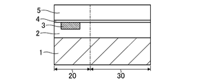
- FIG. 1A is a cross-sectional view for explaining the method for manufacturing the semiconductor device according to the first embodiment.
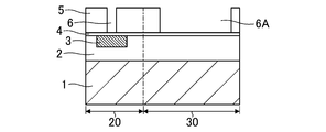
- FIG. 1B is a cross-sectional view for explaining the method for manufacturing the semiconductor device according to the first embodiment.
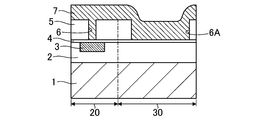
- FIG. 1C is a cross-sectional view for explaining the method for manufacturing the semiconductor device according to the first embodiment.
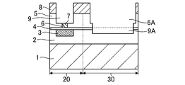
- FIG. 2A is a cross-sectional view for explaining the method for manufacturing the semiconductor device according to the first embodiment.
- FIG. 2B is a cross-sectional view for explaining the method for manufacturing the semiconductor device according to the first embodiment.
- FIG. 2C is a cross-sectional view for explaining the method for manufacturing the semiconductor device according to the first embodiment.
- FIG. 3A is a cross-sectional view for explaining the method for manufacturing the semiconductor device according to the first embodiment.
- FIG. 3B is a cross-sectional view for explaining the method for manufacturing the semiconductor device according to the first embodiment.
- FIG. 3C is a cross-sectional view for explaining the method for manufacturing the semiconductor device according to the first embodiment.
- FIG. 4A is a cross-sectional view for explaining the method for manufacturing the semiconductor device according to the first embodiment.
- FIG. 4B is a cross-sectional view for explaining the method for manufacturing the semiconductor device according to the first embodiment.
- FIG. 4C is a cross-sectional view for explaining the method of manufacturing the semiconductor device according to the first embodiment.
- FIG. 4D is a cross-sectional view for explaining the method of manufacturing the semiconductor device according to the first embodiment.
- FIG. 5A is a cross-sectional view illustrating a method for manufacturing a semiconductor device according to a reference example.
- FIG. 5A is a cross-sectional view illustrating a method for manufacturing a semiconductor device according to a reference example.
- FIG. 5B is a cross-sectional view illustrating the method for manufacturing the semiconductor device according to the reference example.
- FIG. 5C is a cross-sectional view illustrating the method for manufacturing the semiconductor device according to the reference example.
- FIG. 6A is a cross-sectional view illustrating a method for manufacturing a semiconductor device according to a reference example.
- FIG. 6B is a cross-sectional view illustrating the method for manufacturing the semiconductor device according to the reference example.
- FIG. 6C is a cross-sectional view illustrating the method for manufacturing the semiconductor device according to the reference example.
- FIG. 7A is a cross-sectional view illustrating a method for manufacturing a semiconductor device according to a reference example.
- FIG. 7B is a cross-sectional view illustrating the method for manufacturing the semiconductor device according to the reference example.
- FIG. 7C is a cross-sectional view illustrating the method for manufacturing the semiconductor device according to the reference example.
- FIG. 8A is a cross-sectional view illustrating a method for manufacturing a semiconductor device according to a reference example.
- FIG. 8B is a cross-sectional view illustrating the method for manufacturing the semiconductor device according to the reference example.
- FIG. 8C is a cross-sectional view illustrating the method for manufacturing the semiconductor device according to the reference example.
- FIG. 8D is a cross-sectional view illustrating the method for manufacturing the semiconductor device according to the reference example.
- FIG. 9A is a cross-sectional view illustrating the method of manufacturing the semiconductor device according to the second embodiment.
- FIG. 9A is a cross-sectional view illustrating the method of manufacturing the semiconductor device according to the second embodiment.
- FIG. 9B is a cross-sectional view illustrating the method for manufacturing the semiconductor device according to the second embodiment.
- FIG. 9C is a cross-sectional view illustrating the method of manufacturing the semiconductor device according to the second embodiment.
- FIG. 10A is a cross-sectional view illustrating the method for manufacturing the semiconductor device according to the second embodiment.
- FIG. 10B is a cross-sectional view illustrating the method of manufacturing the semiconductor device according to the second embodiment.
- FIG. 10C is a cross-sectional view illustrating the method for manufacturing the semiconductor device according to the second embodiment.
- FIG. 11A is a cross-sectional view illustrating a method for manufacturing a semiconductor device according to another embodiment.
- FIG. 11B is a cross-sectional view for explaining the method for manufacturing a semiconductor device according to another embodiment.
- FIG. 11A is a cross-sectional view illustrating a method for manufacturing a semiconductor device according to another embodiment.
- FIG. 11B is a cross-sectional view for explaining the method for manufacturing a
- FIG. 11C is a cross-sectional view for explaining the method for manufacturing a semiconductor device according to another embodiment.
- FIG. 12A is a cross-sectional view illustrating a method for manufacturing a semiconductor device according to another embodiment.
- FIG. 12B is a cross-sectional view for explaining the method for manufacturing a semiconductor device according to another embodiment.
- FIG. 12C is a cross-sectional view for explaining the method for manufacturing a semiconductor device according to another embodiment.
- FIG. 13A is a cross-sectional view illustrating a method for manufacturing a semiconductor device according to another embodiment.
- FIG. 13B is a cross-sectional view for explaining the method for manufacturing a semiconductor device according to another embodiment.
- FIG. 13C is a cross-sectional view for explaining the method for manufacturing a semiconductor device according to another embodiment.
- FIG. 14A is a cross-sectional view for explaining the method for manufacturing a semiconductor device according to another embodiment.
- FIG. 14B is a cross-sectional view for explaining the method for manufacturing a
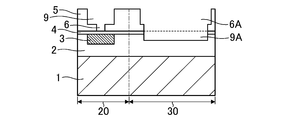
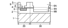
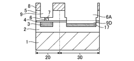
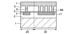
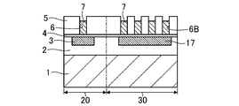
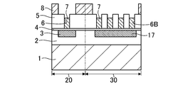
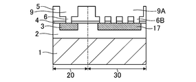
- (First embodiment) -Semiconductor device manufacturing method- 1A to 1C, 2A to 2C, 3A to 3C, and 4A to 4D are cross-sectional views for explaining the method for manufacturing the semiconductor device according to the first embodiment.
- the left side is an element formation region 20 (first region)
- the right side is a pad formation region 30 (second region).
- a method for manufacturing a semiconductor device will be described.
- an insulator such as silicon oxide (SiO 2 ) is formed on the upper surface of the substrate 1 on which the element forming region 20 and the pad forming region 30 are formed by a chemical vapor deposition (CVD) method or the like.
- a first interlayer film 2 is formed.
- a wiring trench is formed on the second interlayer film 2 by known lithography and etching.
- CMP chemical mechanical polishing
- a first liner film 4 made of, for example, silicon carbide (SiC) having a thickness of 60 nm is formed on the first metal wiring 3 and the first interlayer film 2 by a known method.
- a second interlayer film 5 made of silicon oxide and having a thickness of 300 nm is formed on the first interlayer film 2 and the first metal wiring 3 with the first liner film 4 interposed therebetween. Form.
- a via hole 6 penetrating the second interlayer film 5 is formed above the first metal wiring 3 in the element formation region 20 by lithography and etching.
- a pad hole 6 ⁇ / b> A that penetrates the second interlayer film 5 is formed in the pad formation region 30.
- the via hole 6 has a diameter of about 100 nm, and the pad hole 6A has a diameter of about 70 ⁇ m.
- the via hole 6 and the pad hole 6A can be formed by etching using the same mask (not shown). This etching is stopped at the first liner film 4.
- a resist 7 having a thickness of about 300 nm is formed on the substrate. Since the opening area of the via hole 6 in the element formation region 20 is small, the resist 7 is completely embedded in the via hole 6 and is formed to a thickness of approximately 600 nm including the resist in the via hole 6. On the other hand, since the planar area of the pad hole 6A formed in the pad forming region 30 is larger than that of the via hole 6, the thickness of the resist 7 is about 300 nm on the pad hole 6A, and the thickness of the resist 7 on the via hole 6 is increased. It is thinner than that.
- the resist 7 is etched back to remove portions of the resist 7 formed on the second interlayer film 5 and in the pad hole 6A. In this step, the resist 7 remains in the via hole 6, but the resist 7 hardly remains in the pad hole 6A.
- a resist 8 is formed by lithography so that the wiring formation region is opened in the element formation region 20 and the pad formation region 30 is opened above the pad hole 6A.
- the opening provided above the pad hole 6A may have a larger planar area than the pad hole 6A.
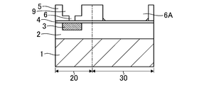
- the second interlayer film 5 is etched using the resist 8 to form a wiring groove 9 in the element formation region 20.
- the depth of the wiring groove 9 is about 180 nm. Since the resist 7 remains in the via hole 6, the first liner film 4 is not etched in the region where the via hole 6 is formed.
- the upper portions of the first liner film 4 and the first interlayer film 2 are removed to form pad recesses 9A.
- the etching amount in the pad recess 9A is about 120 to 150 nm.
- the resists 7 and 8 are removed by washing.
- a portion of the first liner film 4 exposed in the via hole 6 is removed by etching.
- a part of the first interlayer film 2 is removed in the pad formation region 30, thereby forming a pad recess 9 ⁇ / b> B.
- the depth of the pad recess 9B is about 70 nm.
- etching reaction products are removed by washing.
- the shape of the semiconductor device is not changed by the cleaning in this step.
- the height of the first via 10 is about 110 nm, and the height of the second metal wiring 11 is about 120 nm.
- the height (thickness) of the landing pad 12 is about 360 nm to 390 nm.
- a second liner film 13 made of silicon carbide having a thickness of 60 nm is formed on the second interlayer film 5, the second metal wiring 11, and the landing pad 12.
- a passivation film 14 made of silicon nitride and having a thickness of 1000 nm is formed on the second liner film 13 by a known CVD method or the like.
- the processing on the upper surface side of the substrate 1 is once completed.
- the substrate 1 is shaved from the back surface side so that the thickness of the substrate 1 is about 300 to 400 ⁇ m.
- an insulating film 15 made of, for example, a silicon oxide film is formed on the back surface of the substrate 1 so as to cover the element forming region 20.
- the insulating film 15 and the substrate 1 are etched from the back side by lithography and etching.
- a part of the landing pad 12 is etched to form a via hole 16.
- the excess copper is removed by CMP, whereby a TSV (second via) 25 that penetrates the substrate 1 and is connected to the landing pad 12 is formed.
- the metal formed in the via hole 16 may be tungsten (W), aluminum (Al), or the like, or the via hole 16 may not be completely filled with metal.
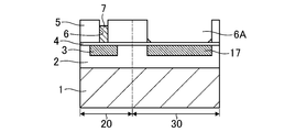
- FIGS. 5A to 5C, FIGS. 6A to 6C, FIGS. 7A to C, and FIGS. 8A to 8D are cross-sectional views illustrating a method of manufacturing a semiconductor device according to a reference example.
- the first interlayer film 2 made of an insulator such as silicon oxide is formed on the upper surface of the substrate 1 on which the element forming region 20 and the pad forming region 30 are formed.
- a wiring trench is formed on the first interlayer film 2 by known lithography and etching.
- a recess having the same depth as the wiring groove in the element formation region 20 is also formed in the pad formation region 30.
- a second interlayer film 5 made of silicon oxide and having a thickness of 300 nm is formed on the first interlayer film 2 and the first metal wiring 3 with the first liner film 4 interposed therebetween.
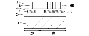
- via holes 6 penetrating the second interlayer film 5 are formed in the element forming region 20, and pad holes 6 ⁇ / b> A are formed above the metal film 17 in the pad forming region 30. .
- a resist 7 having a thickness of about 300 nm is formed on the substrate.
- the resist 7 is embedded in the via hole 6 and the pad hole 6A.
- the resist 7 is etched back to remove portions of the resist 7 formed on the second interlayer film 5 and in the pad hole 6A.
- a resist 8 for wiring formation is formed by lithography.
- a wiring trench 9 is formed in the element formation region 20.
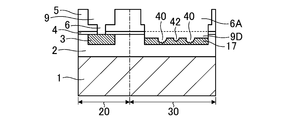
- the first liner film 4 exposed in the pad hole 6A is removed, and the upper portion of the metal film 17 is also removed to form the pad recess 9D. Since the etching rate of copper constituting the metal film 17 is slower than the etching rate of the second interlayer film 5, the depth of the pad recess 9D is set to the pad recess 9A in the semiconductor device of this embodiment (see FIG. 3A). It becomes shallower than In this step, the metal film 17 is greatly damaged by etching.
- the first liner film 4 exposed in the via hole 6 in the element formation region 20 is removed. Also in this step, the metal film 17 is damaged. Subsequently, as shown in FIG. 8A, the reaction product by etching is removed by washing. At this time, a defect 42 is generated in the metal film 17 due to the damage that the metal film 17 receives by etching.
- the pad hole 6A in the pad formation region 30, and the pad recess 9D by plating After the copper is embedded in the via hole 6 and the wiring groove 9 in the element formation region 20, the pad hole 6A in the pad formation region 30, and the pad recess 9D by plating. Then, excess copper is removed by CMP method. As a result, the first via 10 is formed in the via hole 6, and the second metal wiring 11 is formed in the wiring groove 9. In this step, copper is embedded in the pad hole 6A and the pad recess 9D, whereby the landing pad 12B including these copper and the metal film 17 is formed. Therefore, the lower surface position of the landing pad 12B manufactured by the method according to the reference example is equal to the lower surface position of the first metal wiring 3.
- the defects 40 and 42 generated in the metal film 17 during the manufacturing process remain as cavities without being embedded.
- a second liner film 13 made of silicon carbide having a thickness of 60 nm is formed on the second interlayer film 5, the second metal wiring 11, and the landing pad 12B.
- a passivation film 14 made of silicon nitride and having a thickness of 1000 nm is formed on the second liner film 13 by a known CVD method or the like.
- the substrate 1 is shaved from the back surface side so that the thickness of the substrate 1 is about 300 to 400 ⁇ m.
- an insulating film 15 is formed on the back surface of the substrate 1.
- the insulating film 15 and the substrate 1 are etched from the back side by lithography and an etching method.
- a part of the landing pad 12B is etched to form the via hole 16.
- excess copper is removed by CMP to penetrate the substrate 1 and connect a TSV (second via) 25 connected to the landing pad 12B.
- the defects 40 and 42 are generated in the landing pad 12B. Therefore, a connection failure may occur between the landing pad 12B and the TSV 25.
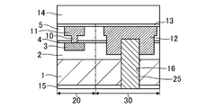
- the position of the lower surface of the landing pad 12 can be set lower than the first metal wiring 3, so that the landing pad 12 can be made thicker than the semiconductor device according to the reference example. It is possible to prevent the landing pad 12 from penetrating when the via hole 16 is formed.
- the formation of the recess for forming the landing pad 12 can be performed simultaneously with the step of forming the wiring groove 9 and the via hole 6, and the formation of the copper film for the landing pad 12 is the second. Since the metal wiring 11 and the first via 10 can be formed at the same time, the landing pad 12 can be formed without increasing the number of steps.
- an element formation region (first region) 20 and a pad formation region (second region) 30 are formed.
- the first interlayer film 2 passes through the second interlayer film 5 and electrically connects the first metal wiring 3 and the second metal wiring 11.
- the semiconductor device of this embodiment is also formed on the second liner film 13 formed on the second interlayer film 5, the second metal wiring 11 and the landing pad 12, and the second liner film 13.
- the passivation film 14 is provided.
- the lower surface position of the landing pad 12 is different from the lower surface position of the first metal wiring 3 and is lower than the lower surface position of the first metal wiring 3.
- the substrate 1 may be made of a semiconductor such as silicon, but is not limited thereto.
- the first interlayer film 2 and the second interlayer film 5 are made of an insulating film such as silicon oxide.
- the first interlayer film 2 and the second interlayer film 5 may be made of an insulator other than silicon oxide, and may be a known low-k film.
- the landing pad 12, the first metal wiring 3 and the second metal wiring 11 may be made of copper or an alloy containing copper as a main component, or may be made of a conductive material other than copper. Good.
- the landing pad 12 may be made of the same material as the second metal wiring 11 and the first via 10.
- the first metal wiring 3, the second metal wiring 11 and the first via, the landing pad 12 and the TSV 25 may each be composed only of copper or the like, but are formed thinly along the inner surface of the wiring groove or recess.
- the barrier metal layer may be composed of two layers of a metal layer made of copper or the like, or may have a structure other than this.
- the thickness of the landing pad 12 is thicker than the total value of the height of the first metal wiring 3, the height of the first via 10, and the height of the second metal wiring 11. ing.
- the landing pad 12 only needs to be provided by using a process of forming two layers of metal wiring adjacent in the vertical direction, and is higher than the total height of at least one layer of metal wiring and vias connected thereto. What is necessary is just to form thickly.
- the thickness of the first interlayer film 2 may be about 400 nm, for example. Further, the landing pad 12 may have a diameter of about 70 ⁇ m and a thickness of about 360 nm to 390 nm.
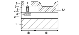
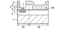
- FIG. 9A to 9C and 10A to 10C are cross-sectional views illustrating a method for manufacturing a semiconductor device according to the second embodiment.
- the method of the present embodiment is the same as the method of the first embodiment up to the step shown in FIG. 2B. Therefore, the process after the process shown in FIG. 2B will be described below.
- a wiring formation region is opened, and in the pad formation region 30, a resist 8 covering the pad hole 6A is formed.
- the second interlayer film 5 is etched using the resist 8 to form a wiring groove 9 in the element formation region 20.
- the first liner film 4 is not etched in the pad formation region 30.
- the resists 7 and 8 are removed by washing.
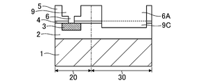
- the portion of the first liner film 4 exposed in the via hole 6 is removed by etching. Simultaneously with the removal of the first liner film 4, a part of the first liner film 4 and a part of the first interlayer film 2 are removed in the pad formation region 30, thereby forming a pad recess 9 ⁇ / b> C.
- the via hole 6 and the wiring groove 9 in the element forming region 20, the pad hole 6 A in the pad forming region 30, and the pad recess 9 C are plated by plating.
- excess copper is removed by CMP method.
- the first via 10 is formed in the via hole 6, and the second metal wiring 11 is formed in the wiring groove 9.
- the landing pad 12 is formed in the pad recess 9C and the pad hole 6A. At this time, the lower surface position of the landing pad 12 is shallower than the lower surface position of the first metal wiring 3.
- the thickness of the landing pad 12 is about 240 nm.
- a second liner film 13 made of silicon carbide having a thickness of 60 nm is formed on the second interlayer film 5, the second metal wiring 11, and the landing pad 12.
- a passivation film 14 made of silicon nitride and having a thickness of 1000 nm is formed on the second liner film 13 by a known CVD method or the like.
- the substrate 1 is shaved from the back side so that the thickness of the substrate 1 is about 300 to 400 ⁇ m.
- an insulating film 15 is formed on the back surface of the substrate 1.
- the insulating film 15 and the substrate 1 are etched from the back side by lithography and etching.
- a part of the landing pad 12 is etched to form a via hole 16.
- the excess copper is removed by CMP, whereby a TSV (second via) 25 that penetrates the substrate 1 and is connected to the landing pad 12 is formed.
- the landing pad 12 is formed of a metal film formed at a time, the metal film is not damaged by etching. For this reason, since no defect occurs in the landing pad 12, a connection failure is less likely to occur between the TSV 25 and the landing pad 12.
- the thickness of the landing pad 12 can be made larger than the total value of the height of the first via 10 and the height of the second metal wiring 11, so that when the TSV 25 is formed. It is difficult for the landing pad 12 to penetrate.
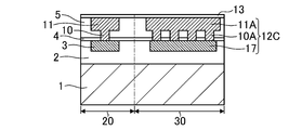
- 11A to 11C, 12A to 12C, 13A to 13C, 14A, and 14B are cross-sectional views illustrating a method for manufacturing a semiconductor device according to another embodiment of the present invention.
- a metal film 17 is provided in the pad forming region 30 at the same depth position as the first metal wiring 3.
- a first liner film 4 is formed on the first metal wiring 3, the metal film 17, and the first interlayer film 2.
- the via hole 6 is formed in the element forming region 20, and the via hole 6 ⁇ / b> B is formed in the pad forming region 30.
- the diameters of the via hole 6 and the via hole 6B are the same.
- a resist 7 is formed on the substrate.
- a resist 7 is embedded in the via holes 6 and 6B.
- the resist 7 is etched back to partially leave the resist 7 in the via holes 6 and 6B.
- a resist 8 for forming a wiring groove is formed on the second interlayer film 5. At this time, an opening is formed in the resist 8 in a region where the via hole 6B is formed.
- the second interlayer film 5 is etched using the resist 8 as a mask to form a wiring groove 9. Since the resist 7 remains in the via hole 6B, the metal film 17 is not exposed in this step. By this step, the pad hole 9E is formed in the pad forming region 30.
- the resists 7 and 8 are removed by cleaning.
- the exposed portions of the first liner film 4 are removed by etching in the element formation region 20 and the pad formation region 30.
- the substrate is cleaned.
- the metal film 17 is not easily damaged by etching. For this reason, in the process shown in FIG. 13B, defects are less likely to occur in the metal film 17.
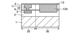
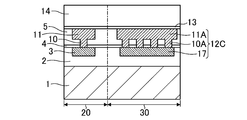
- the excess copper is removed by the CMP method, whereby the first via 10 and the second metal wiring 11, the third via 10A and the metal film 11A are formed.
- the metal film 17, the third via 10A, and the metal film 11A constitute a landing pad 12C.
- a second liner film 13 made of silicon carbide having a thickness of 60 nm is formed on the second interlayer film 5, the second metal wiring 11, and the landing pad 12.
- a passivation film 14 made of silicon nitride and having a thickness of 1000 nm is formed on the second liner film 13 by a known CVD method or the like.
- the substrate 1 is shaved from the back surface side so that the thickness of the substrate 1 is about 300 to 400 ⁇ m.
- an insulating film 15 is formed on the back surface of the substrate 1.
- the insulating film 15 and the substrate 1 are etched from the back side by lithography and etching.
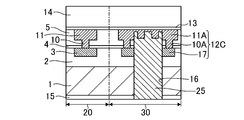
- a part of the first liner film 4 and the second interlayer film 5 is removed, and a part of the landing pad 12C is etched to form a via hole 16.
- excess copper is removed by CMP to penetrate the substrate 1 and connect the TSV (second via) 25 to the landing pad 12C.
- the first liner film 4 and the second interlayer film 5 exist between the via holes 6B in the pad formation region 30, when forming the via holes 16, It is difficult to reliably stop etching on the landing pad 12C.
- the semiconductor device and the manufacturing method thereof described above are examples of the embodiment, and the configuration of the semiconductor device, the thickness, size, material, and the like of each layer can be changed as appropriate.
- the size of the opening of the resist 8 in the pad formation region 30 may be larger than the pad hole 6A, but may be the same size as the pad hole 6A or smaller than the pad hole 6A.
- the semiconductor device and the manufacturing method thereof according to the present invention can be applied to various semiconductor devices provided with a TSV structure.
Landscapes
- Internal Circuitry In Semiconductor Integrated Circuit Devices (AREA)
Abstract
Description
-半導体装置の製造方法-
図1A~C、図2A~C、図3A~C及び図4A~Dは、第1の実施形態に係る半導体装置の製造方法を説明するための断面図である。これらの図では、左側が素子形成領域20(第1の領域)、右側がパッド形成領域30(第2の領域)となっている。以下、半導体装置の製造方法を説明する。
以上の方法によって作製される本実施形態実施形態の半導体装置は、図4Dに示すように、素子形成領域(第1の領域)20と、パッド形成領域(第2の領域)30とが形成された基板1と、基板1の上面上に形成された第1の層間膜2と、素子形成領域20において、第1の層間膜2の上部に埋め込まれた第1の金属配線3と、第1の層間膜2上及び第1の金属配線3上に形成された第2の層間膜5と、素子形成領域20において、第2の層間膜5の上部に埋め込まれた第2の金属配線11と、第2の層間膜5を貫通し、第1の金属配線3と第2の金属配線11とを電気的に接続する第1のビア10と、パッド形成領域30において、第1の層間膜2の上部に埋め込まれるとともに、第2の層間膜5を貫通するランディングパッド12と、パッド形成領域30において、基板1の裏面側から基板1及び第1の層間膜2を貫通し、ランディングパッド12に接続するTSV(第2のビア)25とを備えている。本実施形態の半導体装置はまた、第2の層間膜5上、第2の金属配線11上及びランディングパッド12上に形成された第2のライナー膜13と、第2のライナー膜13上に形成されたパッシベーション膜14とを備えている。
本発明の第2の実施形態に係る半導体装置の製造方法を説明する。
図11A~C、図12A~C、図13A~C、図14A、Bは、本発明の他の実施形態に係る半導体装置の製造方法を説明する断面図である。
2 第1の層間膜
3 第1の金属配線
4 第1のライナー膜
5 第2の層間膜
6、6B ビアホール
6A パッド用孔
7、8 レジスト
9 配線溝
9A、9B、9C、9D パッド用凹部
9E パッド用孔
10 第1のビア
10A 第3のビア
11 第2の金属配線
11A 金属膜
12、12B、12C ランディングパッド
13 第2のライナー膜
14 パッシベーション膜
15 絶縁膜
16 ビアホール
17 金属膜
20 素子形成領域
25 TSV
30 パッド形成領域
40、42 欠陥
Claims (8)
- 第1の領域と、第2の領域とが形成された基板と、
前記基板の上面上に形成された第1の層間膜と、
前記第1の領域において、前記第1の層間膜の上部に埋め込まれた第1の金属配線と、
前記第1の層間膜上及び前記第1の金属配線上に形成された第2の層間膜と、
前記第1の領域において、前記第2の層間膜の上部に埋め込まれた第2の金属配線と、
前記第2の層間膜を貫通し、前記第1の金属配線と前記第2の金属配線とを電気的に接続する第1のビアと、
前記第2の領域において、前記第1の層間膜の上部に埋め込まれるとともに、前記第2の層間膜を貫通するランディングパッドと、
前記第2の領域において、前記基板の裏面側から前記基板及び前記第1の層間膜を貫通し、前記ランディングパッドに接続する第2のビアとを備え、
前記ランディングパッドの下面位置は、前記第1の金属配線の下面位置と異なっている半導体装置。 - 請求項1において、
前記第1のビアと前記第2の金属配線とは同一の材料で構成されており、
前記ランディングパッドは、前記第1の層間膜の上部から前記第2の層間膜内に亘って設けられ、且つ前記第1のビア及び前記第2の金属配線と同一の材料で構成されている金属膜を有していることを特徴とする半導体装置。 - 請求項1又は2において、
前記ランディングパッドの下面位置は、前記第1の金属配線の下面位置よりも低く、前記ランディングパッドの厚みは、前記第1の金属配線の高さと、前記第1のビアの高さと、前記第2の金属配線の高さとの和よりも厚いことを特徴とする半導体装置。 - 第1の領域と第2の領域とが形成された基板の上面上に第1の層間膜と、前記第1の層間膜の上部に埋め込まれた第1の金属配線とを形成する工程と、
前記第1の層間膜上及び前記第1の金属配線上に、第2の層間膜を形成する工程と、
前記第1の領域において、前記第2の層間膜内の配線溝と、前記第1の金属配線の上方で前記第2の層間膜を貫通する第1のビアホールとをそれぞれ形成する工程と、
前記配線溝及び前記第1のビアホールを形成する際に、前記第2の領域において、前記第1の層間膜の上部にパッド用凹部を形成するとともに、前記第2の層間膜を貫通するパッド用孔を形成する工程と、
前記第1のビアホール、前記配線溝、前記パッド用凹部及び前記パッド用孔内に金属を埋め込むことによって前記第1のビアホール内に第1のビアを形成するとともに、前記配線溝内に第2の金属配線を形成し、且つ前記パッド用凹部及び前記パッド用孔内にランディングパッドを形成する工程と、
前記第2の領域において、前記基板の裏面側から前記基板及び前記第1の層間膜を貫通し、前記ランディングパッドに接続する第2のビアを形成する工程とを備えている半導体装置の製造方法。 - 請求項4において、
前記第1のビアホールを形成するのと同時に、前記パッド用孔を形成し、
前記配線溝を形成するのと同時に、前記パッド用凹部の少なくとも一部を形成することを特徴とする半導体装置の製造方法。 - 請求項4において、
前記第1の金属配線を形成する工程の後、前記第2の層間膜を形成する工程の前に、前記第1の金属配線上及び前記第1の層間膜上に絶縁体からなるライナー膜を形成する工程をさらに備えており、
前記第1のビアホールを形成するのと同時に、前記パッド用孔を形成し、
前記ライナー膜のうち前記第1のビアホールによって露出された部分を除去するのと同時に、前記第2の領域において前記パッド用凹部を形成することを特徴とする半導体装置の製造方法。 - 請求項4~6のうちいずれか1つにおいて、
前記第1の金属配線の下面高さと前記ランディングパッドの下面高さとは互いに異なっていることを特徴とする半導体装置の製造方法。 - 請求項4~7のうちいずれか1つにおいて、
前記第1のビアホールを形成する工程では、前記第2の領域内の前記第2の層間膜に、前記第1のビアよりも大きい直径を有する第3のビアを形成することを特徴とする半導体装置の製造方法。
Priority Applications (5)
| Application Number | Priority Date | Filing Date | Title |
|---|---|---|---|
| CN201780010885.5A CN108701614A (zh) | 2016-02-29 | 2017-02-10 | 半导体装置及其制造方法 |
| JP2018503002A JP6568994B2 (ja) | 2016-02-29 | 2017-02-10 | 半導体装置及びその製造方法 |
| EP17759617.8A EP3407376B1 (en) | 2016-02-29 | 2017-02-10 | Semiconductor device and method for manufacturing same |
| KR1020187025368A KR102116060B1 (ko) | 2016-02-29 | 2017-02-10 | 반도체 장치 및 그 제조방법 |
| US16/114,303 US10483125B2 (en) | 2016-02-29 | 2018-08-28 | Semiconductor device and method for manufacturing same |
Applications Claiming Priority (2)
| Application Number | Priority Date | Filing Date | Title |
|---|---|---|---|
| JP2016-036622 | 2016-02-29 | ||
| JP2016036622 | 2016-02-29 |
Related Child Applications (1)
| Application Number | Title | Priority Date | Filing Date |
|---|---|---|---|
| US16/114,303 Continuation US10483125B2 (en) | 2016-02-29 | 2018-08-28 | Semiconductor device and method for manufacturing same |
Publications (1)
| Publication Number | Publication Date |
|---|---|
| WO2017150146A1 true WO2017150146A1 (ja) | 2017-09-08 |
Family
ID=59742781
Family Applications (1)
| Application Number | Title | Priority Date | Filing Date |
|---|---|---|---|
| PCT/JP2017/004961 Ceased WO2017150146A1 (ja) | 2016-02-29 | 2017-02-10 | 半導体装置及びその製造方法 |
Country Status (6)
| Country | Link |
|---|---|
| US (1) | US10483125B2 (ja) |
| EP (1) | EP3407376B1 (ja) |
| JP (1) | JP6568994B2 (ja) |
| KR (1) | KR102116060B1 (ja) |
| CN (1) | CN108701614A (ja) |
| WO (1) | WO2017150146A1 (ja) |
Cited By (30)
| Publication number | Priority date | Publication date | Assignee | Title |
|---|---|---|---|---|
| US10158038B1 (en) | 2018-05-17 | 2018-12-18 | Hi Llc | Fast-gated photodetector architectures comprising dual voltage sources with a switch configuration |
| US10340408B1 (en) | 2018-05-17 | 2019-07-02 | Hi Llc | Non-invasive wearable brain interface systems including a headgear and a plurality of self-contained photodetector units configured to removably attach to the headgear |
| US10515993B2 (en) | 2018-05-17 | 2019-12-24 | Hi Llc | Stacked photodetector assemblies |
| US10868207B1 (en) | 2019-06-06 | 2020-12-15 | Hi Llc | Photodetector systems with low-power time-to-digital converter architectures to determine an arrival time of photon at a photodetector based on event detection time window |
| US11006876B2 (en) | 2018-12-21 | 2021-05-18 | Hi Llc | Biofeedback for awareness and modulation of mental state using a non-invasive brain interface system and method |
| US11081611B2 (en) | 2019-05-21 | 2021-08-03 | Hi Llc | Photodetector architectures for efficient fast-gating comprising a control system controlling a current drawn by an array of photodetectors with a single photon avalanche diode |
| US11096620B1 (en) | 2020-02-21 | 2021-08-24 | Hi Llc | Wearable module assemblies for an optical measurement system |
| US11187575B2 (en) | 2020-03-20 | 2021-11-30 | Hi Llc | High density optical measurement systems with minimal number of light sources |
| US11245404B2 (en) | 2020-03-20 | 2022-02-08 | Hi Llc | Phase lock loop circuit based signal generation in an optical measurement system |
| US11515014B2 (en) | 2020-02-21 | 2022-11-29 | Hi Llc | Methods and systems for initiating and conducting a customized computer-enabled brain research study |
| US11607132B2 (en) | 2020-03-20 | 2023-03-21 | Hi Llc | Temporal resolution control for temporal point spread function generation in an optical measurement system |
| US11630310B2 (en) | 2020-02-21 | 2023-04-18 | Hi Llc | Wearable devices and wearable assemblies with adjustable positioning for use in an optical measurement system |
| US11645483B2 (en) | 2020-03-20 | 2023-05-09 | Hi Llc | Phase lock loop circuit based adjustment of a measurement time window in an optical measurement system |
| US11771362B2 (en) | 2020-02-21 | 2023-10-03 | Hi Llc | Integrated detector assemblies for a wearable module of an optical measurement system |
| US11813041B2 (en) | 2019-05-06 | 2023-11-14 | Hi Llc | Photodetector architectures for time-correlated single photon counting |
| US11819311B2 (en) | 2020-03-20 | 2023-11-21 | Hi Llc | Maintaining consistent photodetector sensitivity in an optical measurement system |
| US11857348B2 (en) | 2020-03-20 | 2024-01-02 | Hi Llc | Techniques for determining a timing uncertainty of a component of an optical measurement system |
| US11864867B2 (en) | 2020-03-20 | 2024-01-09 | Hi Llc | Control circuit for a light source in an optical measurement system by applying voltage with a first polarity to start an emission of a light pulse and applying voltage with a second polarity to stop the emission of the light pulse |
| US11877825B2 (en) | 2020-03-20 | 2024-01-23 | Hi Llc | Device enumeration in an optical measurement system |
| US11883181B2 (en) | 2020-02-21 | 2024-01-30 | Hi Llc | Multimodal wearable measurement systems and methods |
| US11903676B2 (en) | 2020-03-20 | 2024-02-20 | Hi Llc | Photodetector calibration of an optical measurement system |
| US11950879B2 (en) | 2020-02-21 | 2024-04-09 | Hi Llc | Estimation of source-detector separation in an optical measurement system |
| US11969259B2 (en) | 2020-02-21 | 2024-04-30 | Hi Llc | Detector assemblies for a wearable module of an optical measurement system and including spring-loaded light-receiving members |
| US12029558B2 (en) | 2020-02-21 | 2024-07-09 | Hi Llc | Time domain-based optical measurement systems and methods configured to measure absolute properties of tissue |
| US12059270B2 (en) | 2020-04-24 | 2024-08-13 | Hi Llc | Systems and methods for noise removal in an optical measurement system |
| US12059262B2 (en) | 2020-03-20 | 2024-08-13 | Hi Llc | Maintaining consistent photodetector sensitivity in an optical measurement system |
| US12085789B2 (en) | 2020-03-20 | 2024-09-10 | Hi Llc | Bias voltage generation in an optical measurement system |
| US12138068B2 (en) | 2020-03-20 | 2024-11-12 | Hi Llc | Techniques for characterizing a nonlinearity of a time-to-digital converter in an optical measurement system |
| US12144653B2 (en) | 2020-02-21 | 2024-11-19 | Hi Llc | Systems, circuits, and methods for reducing common-mode noise in biopotential recordings |
| WO2026084990A1 (en) * | 2024-10-15 | 2026-04-23 | Lam Research Corporation | Etching through silicon vias having different sizes with minimum depth loading |
Families Citing this family (6)
| Publication number | Priority date | Publication date | Assignee | Title |
|---|---|---|---|---|
| US10163758B1 (en) * | 2017-10-30 | 2018-12-25 | Taiwan Semiconductor Manufacturing Company Ltd. | Semiconductor structure and manufacturing method for the same |
| US10420498B1 (en) | 2018-06-20 | 2019-09-24 | Hi Llc | Spatial and temporal-based diffusive correlation spectroscopy systems and methods |
| US11213206B2 (en) | 2018-07-17 | 2022-01-04 | Hi Llc | Non-invasive measurement systems with single-photon counting camera |
| KR102793910B1 (ko) | 2020-03-26 | 2025-04-08 | 삼성전자주식회사 | 관통 실리콘 비아를 포함하는 집적 회로 반도체 소자 |
| US12322679B2 (en) * | 2021-03-18 | 2025-06-03 | Taiwan Semiconductor Manufacturing Company Limited | Semiconductor die including through substrate via barrier structure and methods for forming the same |
| US12506050B1 (en) | 2024-11-06 | 2025-12-23 | Globalfoundries Singapore Pte. Ltd. | Face bonded semiconductor device with through oxide via and metal plug |
Citations (5)
| Publication number | Priority date | Publication date | Assignee | Title |
|---|---|---|---|---|
| WO2009107742A1 (ja) * | 2008-02-28 | 2009-09-03 | 日本電気株式会社 | 半導体装置 |
| JP2012028696A (ja) * | 2010-07-27 | 2012-02-09 | Fujitsu Semiconductor Ltd | 半導体装置の製造方法 |
| JP2013077711A (ja) * | 2011-09-30 | 2013-04-25 | Sony Corp | 半導体装置および半導体装置の製造方法 |
| JP2014072296A (ja) * | 2012-09-28 | 2014-04-21 | Canon Inc | 半導体装置 |
| JP2015079961A (ja) | 2013-10-15 | 2015-04-23 | 三星電子株式会社Samsung Electronics Co.,Ltd. | Tsv構造を具備した集積回路素子及びその製造方法 |
Family Cites Families (8)
| Publication number | Priority date | Publication date | Assignee | Title |
|---|---|---|---|---|
| TW582095B (en) * | 2003-04-10 | 2004-04-01 | Nanya Technology Corp | Bit line contact and method for forming the same |
| JP5034740B2 (ja) * | 2007-07-23 | 2012-09-26 | ルネサスエレクトロニクス株式会社 | 半導体装置及びその製造方法 |
| JP5656341B2 (ja) * | 2007-10-29 | 2015-01-21 | ピーエスフォー ルクスコ エスエイアールエルPS4 Luxco S.a.r.l. | 半導体装置およびその製造方法 |
| US8860147B2 (en) * | 2007-11-26 | 2014-10-14 | Texas Instruments Incorporated | Semiconductor interconnect |
| US7786584B2 (en) * | 2007-11-26 | 2010-08-31 | Infineon Technologies Ag | Through substrate via semiconductor components |
| US8749028B2 (en) * | 2009-07-01 | 2014-06-10 | Hitachi, Ltd. | Semiconductor device with silicon through electrode and moisture barrier |
| US9293366B2 (en) * | 2010-04-28 | 2016-03-22 | Taiwan Semiconductor Manufacturing Company, Ltd. | Through-substrate vias with improved connections |
| US9219032B2 (en) * | 2012-07-09 | 2015-12-22 | Qualcomm Incorporated | Integrating through substrate vias from wafer backside layers of integrated circuits |
-
2017
- 2017-02-10 JP JP2018503002A patent/JP6568994B2/ja active Active
- 2017-02-10 KR KR1020187025368A patent/KR102116060B1/ko not_active Expired - Fee Related
- 2017-02-10 WO PCT/JP2017/004961 patent/WO2017150146A1/ja not_active Ceased
- 2017-02-10 CN CN201780010885.5A patent/CN108701614A/zh active Pending
- 2017-02-10 EP EP17759617.8A patent/EP3407376B1/en not_active Not-in-force
-
2018
- 2018-08-28 US US16/114,303 patent/US10483125B2/en active Active
Patent Citations (5)
| Publication number | Priority date | Publication date | Assignee | Title |
|---|---|---|---|---|
| WO2009107742A1 (ja) * | 2008-02-28 | 2009-09-03 | 日本電気株式会社 | 半導体装置 |
| JP2012028696A (ja) * | 2010-07-27 | 2012-02-09 | Fujitsu Semiconductor Ltd | 半導体装置の製造方法 |
| JP2013077711A (ja) * | 2011-09-30 | 2013-04-25 | Sony Corp | 半導体装置および半導体装置の製造方法 |
| JP2014072296A (ja) * | 2012-09-28 | 2014-04-21 | Canon Inc | 半導体装置 |
| JP2015079961A (ja) | 2013-10-15 | 2015-04-23 | 三星電子株式会社Samsung Electronics Co.,Ltd. | Tsv構造を具備した集積回路素子及びその製造方法 |
Non-Patent Citations (1)
| Title |
|---|
| See also references of EP3407376A4 |
Cited By (38)
| Publication number | Priority date | Publication date | Assignee | Title |
|---|---|---|---|---|
| US11437538B2 (en) | 2018-05-17 | 2022-09-06 | Hi Llc | Wearable brain interface systems including a headgear and a plurality of photodetector units each housing a photodetector configured to be controlled by a master control unit |
| US10340408B1 (en) | 2018-05-17 | 2019-07-02 | Hi Llc | Non-invasive wearable brain interface systems including a headgear and a plurality of self-contained photodetector units configured to removably attach to the headgear |
| US10424683B1 (en) | 2018-05-17 | 2019-09-24 | Hi Llc | Photodetector comprising a single photon avalanche diode and a capacitor |
| US10515993B2 (en) | 2018-05-17 | 2019-12-24 | Hi Llc | Stacked photodetector assemblies |
| US10672935B2 (en) | 2018-05-17 | 2020-06-02 | Hi Llc | Non-invasive wearable brain interface systems including a headgear and a plurality of self-contained photodetector units |
| US10672936B2 (en) | 2018-05-17 | 2020-06-02 | Hi Llc | Wearable systems with fast-gated photodetector architectures having a single photon avalanche diode and capacitor |
| US10847563B2 (en) | 2018-05-17 | 2020-11-24 | Hi Llc | Wearable systems with stacked photodetector assemblies |
| US10158038B1 (en) | 2018-05-17 | 2018-12-18 | Hi Llc | Fast-gated photodetector architectures comprising dual voltage sources with a switch configuration |
| US11004998B2 (en) | 2018-05-17 | 2021-05-11 | Hi Llc | Wearable brain interface systems including a headgear and a plurality of photodetector units |
| US11903713B2 (en) | 2018-12-21 | 2024-02-20 | Hi Llc | Biofeedback for awareness and modulation of mental state using a non-invasive brain interface system and method |
| US11006876B2 (en) | 2018-12-21 | 2021-05-18 | Hi Llc | Biofeedback for awareness and modulation of mental state using a non-invasive brain interface system and method |
| US11813041B2 (en) | 2019-05-06 | 2023-11-14 | Hi Llc | Photodetector architectures for time-correlated single photon counting |
| US11081611B2 (en) | 2019-05-21 | 2021-08-03 | Hi Llc | Photodetector architectures for efficient fast-gating comprising a control system controlling a current drawn by an array of photodetectors with a single photon avalanche diode |
| US10868207B1 (en) | 2019-06-06 | 2020-12-15 | Hi Llc | Photodetector systems with low-power time-to-digital converter architectures to determine an arrival time of photon at a photodetector based on event detection time window |
| US11398578B2 (en) | 2019-06-06 | 2022-07-26 | Hi Llc | Photodetector systems with low-power time-to-digital converter architectures to determine an arrival time of photon at a photodetector based on event detection time window |
| US11515014B2 (en) | 2020-02-21 | 2022-11-29 | Hi Llc | Methods and systems for initiating and conducting a customized computer-enabled brain research study |
| US11883181B2 (en) | 2020-02-21 | 2024-01-30 | Hi Llc | Multimodal wearable measurement systems and methods |
| US12029558B2 (en) | 2020-02-21 | 2024-07-09 | Hi Llc | Time domain-based optical measurement systems and methods configured to measure absolute properties of tissue |
| US11630310B2 (en) | 2020-02-21 | 2023-04-18 | Hi Llc | Wearable devices and wearable assemblies with adjustable positioning for use in an optical measurement system |
| US11969259B2 (en) | 2020-02-21 | 2024-04-30 | Hi Llc | Detector assemblies for a wearable module of an optical measurement system and including spring-loaded light-receiving members |
| US11771362B2 (en) | 2020-02-21 | 2023-10-03 | Hi Llc | Integrated detector assemblies for a wearable module of an optical measurement system |
| US12144653B2 (en) | 2020-02-21 | 2024-11-19 | Hi Llc | Systems, circuits, and methods for reducing common-mode noise in biopotential recordings |
| US11950879B2 (en) | 2020-02-21 | 2024-04-09 | Hi Llc | Estimation of source-detector separation in an optical measurement system |
| US11096620B1 (en) | 2020-02-21 | 2021-08-24 | Hi Llc | Wearable module assemblies for an optical measurement system |
| US11607132B2 (en) | 2020-03-20 | 2023-03-21 | Hi Llc | Temporal resolution control for temporal point spread function generation in an optical measurement system |
| US11245404B2 (en) | 2020-03-20 | 2022-02-08 | Hi Llc | Phase lock loop circuit based signal generation in an optical measurement system |
| US11864867B2 (en) | 2020-03-20 | 2024-01-09 | Hi Llc | Control circuit for a light source in an optical measurement system by applying voltage with a first polarity to start an emission of a light pulse and applying voltage with a second polarity to stop the emission of the light pulse |
| US11857348B2 (en) | 2020-03-20 | 2024-01-02 | Hi Llc | Techniques for determining a timing uncertainty of a component of an optical measurement system |
| US11903676B2 (en) | 2020-03-20 | 2024-02-20 | Hi Llc | Photodetector calibration of an optical measurement system |
| US11819311B2 (en) | 2020-03-20 | 2023-11-21 | Hi Llc | Maintaining consistent photodetector sensitivity in an optical measurement system |
| US11645483B2 (en) | 2020-03-20 | 2023-05-09 | Hi Llc | Phase lock loop circuit based adjustment of a measurement time window in an optical measurement system |
| US11877825B2 (en) | 2020-03-20 | 2024-01-23 | Hi Llc | Device enumeration in an optical measurement system |
| US11187575B2 (en) | 2020-03-20 | 2021-11-30 | Hi Llc | High density optical measurement systems with minimal number of light sources |
| US12059262B2 (en) | 2020-03-20 | 2024-08-13 | Hi Llc | Maintaining consistent photodetector sensitivity in an optical measurement system |
| US12085789B2 (en) | 2020-03-20 | 2024-09-10 | Hi Llc | Bias voltage generation in an optical measurement system |
| US12138068B2 (en) | 2020-03-20 | 2024-11-12 | Hi Llc | Techniques for characterizing a nonlinearity of a time-to-digital converter in an optical measurement system |
| US12059270B2 (en) | 2020-04-24 | 2024-08-13 | Hi Llc | Systems and methods for noise removal in an optical measurement system |
| WO2026084990A1 (en) * | 2024-10-15 | 2026-04-23 | Lam Research Corporation | Etching through silicon vias having different sizes with minimum depth loading |
Also Published As
| Publication number | Publication date |
|---|---|
| EP3407376B1 (en) | 2020-04-01 |
| EP3407376A4 (en) | 2019-03-27 |
| JP6568994B2 (ja) | 2019-08-28 |
| US10483125B2 (en) | 2019-11-19 |
| KR20180110011A (ko) | 2018-10-08 |
| CN108701614A (zh) | 2018-10-23 |
| JPWO2017150146A1 (ja) | 2018-12-20 |
| KR102116060B1 (ko) | 2020-05-27 |
| EP3407376A1 (en) | 2018-11-28 |
| US20180366342A1 (en) | 2018-12-20 |
Similar Documents
| Publication | Publication Date | Title |
|---|---|---|
| JP6568994B2 (ja) | 半導体装置及びその製造方法 | |
| JP4102246B2 (ja) | 半導体装置及びその製造方法 | |
| JP5096278B2 (ja) | 半導体装置及び半導体装置の製造方法 | |
| CN105575828B (zh) | 一种半导体器件的制作方法 | |
| WO2010035481A1 (ja) | 半導体装置および半導体装置の製造方法 | |
| CN110120372A (zh) | 具有衬底通孔结构的器件及其形成方法 | |
| JP2012038961A (ja) | 半導体装置及び半導体装置の製造方法 | |
| JP2015167153A (ja) | 集積回路装置及びその製造方法 | |
| CN107564850A (zh) | 互连结构及其制造方法 | |
| JP4338614B2 (ja) | 半導体装置およびその製造方法 | |
| JP5377657B2 (ja) | 半導体装置の製造方法 | |
| JP4231055B2 (ja) | 半導体装置及びその製造方法 | |
| JP5078823B2 (ja) | 半導体装置 | |
| JP4646591B2 (ja) | 半導体装置及びその製造方法 | |
| JP2005116788A (ja) | 半導体装置 | |
| JP4110829B2 (ja) | 半導体装置の製造方法 | |
| JP2006093402A (ja) | 半導体装置の製造方法 | |
| JP5424551B2 (ja) | 半導体装置 | |
| CN101501837B (zh) | 一种用于铜工艺无边导通孔的自对准氮化硅覆层方法 | |
| KR100781422B1 (ko) | 듀얼 다마신 패턴 형성 방법 | |
| KR100789612B1 (ko) | 금속 배선 형성 방법 | |
| JP2009038080A (ja) | 半導体装置及びその製造方法 | |
| JP2008124070A (ja) | 半導体装置 | |
| JP2002134609A (ja) | 半導体装置及びその製造方法 | |
| JP2008021865A (ja) | 配線構造、半導体装置、配線の製造方法および半導体装置の製造方法 |
Legal Events
| Date | Code | Title | Description |
|---|---|---|---|
| WWE | Wipo information: entry into national phase |
Ref document number: 2018503002 Country of ref document: JP |
|
| WWE | Wipo information: entry into national phase |
Ref document number: 2017759617 Country of ref document: EP |
|
| NENP | Non-entry into the national phase |
Ref country code: DE |
|
| ENP | Entry into the national phase |
Ref document number: 20187025368 Country of ref document: KR Kind code of ref document: A |
|
| ENP | Entry into the national phase |
Ref document number: 2017759617 Country of ref document: EP Effective date: 20180824 |