WO2017152811A1 - 光噪去除电路、光接收器以及光芯片 - Google Patents
光噪去除电路、光接收器以及光芯片 Download PDFInfo
- Publication number
- WO2017152811A1 WO2017152811A1 PCT/CN2017/075622 CN2017075622W WO2017152811A1 WO 2017152811 A1 WO2017152811 A1 WO 2017152811A1 CN 2017075622 W CN2017075622 W CN 2017075622W WO 2017152811 A1 WO2017152811 A1 WO 2017152811A1
- Authority
- WO
- WIPO (PCT)
- Prior art keywords
- unit
- coupled
- signal
- noise
- voltage
- Prior art date
- Legal status (The legal status is an assumption and is not a legal conclusion. Google has not performed a legal analysis and makes no representation as to the accuracy of the status listed.)
- Ceased
Links
Classifications
-
- H—ELECTRICITY
- H04—ELECTRIC COMMUNICATION TECHNIQUE
- H04B—TRANSMISSION
- H04B10/00—Transmission systems employing electromagnetic waves other than radio-waves, e.g. infrared, visible or ultraviolet light, or employing corpuscular radiation, e.g. quantum communication
- H04B10/60—Receivers
- H04B10/66—Non-coherent receivers, e.g. using direct detection
- H04B10/69—Electrical arrangements in the receiver
- H04B10/697—Arrangements for reducing noise and distortion
-
- H—ELECTRICITY
- H04—ELECTRIC COMMUNICATION TECHNIQUE
- H04B—TRANSMISSION
- H04B10/00—Transmission systems employing electromagnetic waves other than radio-waves, e.g. infrared, visible or ultraviolet light, or employing corpuscular radiation, e.g. quantum communication
- H04B10/11—Arrangements specific to free-space transmission, i.e. transmission through air or vacuum
- H04B10/114—Indoor or close-range type systems
- H04B10/116—Visible light communication
-
- H—ELECTRICITY
- H04—ELECTRIC COMMUNICATION TECHNIQUE
- H04B—TRANSMISSION
- H04B10/00—Transmission systems employing electromagnetic waves other than radio-waves, e.g. infrared, visible or ultraviolet light, or employing corpuscular radiation, e.g. quantum communication
- H04B10/60—Receivers
-
- H—ELECTRICITY
- H04—ELECTRIC COMMUNICATION TECHNIQUE
- H04B—TRANSMISSION
- H04B10/00—Transmission systems employing electromagnetic waves other than radio-waves, e.g. infrared, visible or ultraviolet light, or employing corpuscular radiation, e.g. quantum communication
- H04B10/60—Receivers
- H04B10/66—Non-coherent receivers, e.g. using direct detection
- H04B10/69—Electrical arrangements in the receiver
- H04B10/697—Arrangements for reducing noise and distortion
- H04B10/6972—Arrangements for reducing noise and distortion using passive filtering
Definitions
- the present invention relates to visible light communication technologies, and more particularly to a light noise removal circuit, an optical receiver, and an optical chip.
- Visible light communication technology is a kind of LED
- a new type of wireless optical communication technology developed in technology Communication is carried out by high-frequency flickering of the LED light source, and the transmission rate of visible light communication is up to gigabits per second.
- Visible light communication has a very rich spectrum of resources, which is unmatched by general wireless communications, including microwave communications.
- visible light communication can be applied to any communication protocol, suitable for any environment, and the device for visible light communication is flexible and convenient to install, and is suitable for mass popularization applications.
- a visible light communication system uses visible light for short-range communication, and the visible light has high directivity and cannot penetrate obstacles, and has higher security than wireless communication.
- some visible light communication systems have been applied, such as photon access control systems and photon payment in photonics Internet of Things.
- the mobile phone's flash function can be used as a photonic client, which greatly reduces the application threshold of visible light communication, and since the mobile phone is originally carried by the user, it is not It puts an extra burden on the user.
- visible light communication using a portable photonic client such as a mobile phone is generally in an environment with ambient light.
- the photon receiving end receives the optical signal from the photonic client and converts the optical signal into a meaningful electrical signal by photoelectric conversion.
- the photon receiving end will still convert the unquestioned ambient light into a useless electrical signal.
- These useless electrical signals are noise signals that interfere with the photon receiver correctly receiving the photon client.
- Optical signal is generally in an environment with ambient light.
- a light noise removing circuit including: a noise filtering unit, the noise An input end of the sound filtering unit receives an electrical signal from the photoelectric conversion unit, the noise filtering unit is configured to filter out a noise electrical signal generated by the ambient light in the electrical signal and output a target pulse signal at the output end; and a comparison unit, The first input end of the comparison unit is coupled to the output end of the noise filter unit to receive the target pulse signal, and the comparison unit is configured to output a digital signal according to a comparison between the target pulse signal and a reference voltage.
- an optical receiver comprising: a photoelectric conversion unit for receiving an optical signal and generating an electrical signal by photoelectric conversion; a noise filtering unit, the noise filtering unit And coupled to the photoelectric conversion unit, the noise filtering unit is configured to filter out a noise electrical signal generated by the ambient light in the electrical signal and output a target pulse signal at the output end; and a comparing unit, the first input end of the comparing unit An output end of the noise filtering unit is coupled to receive the target pulse signal, and the comparing unit is configured to output a digital signal according to a comparison between the target pulse signal and a reference voltage
- an optical chip comprising: a photoelectric conversion unit configured to receive an optical signal and generate an electrical signal by photoelectric conversion; a photo noise removing unit, the optical noise a removing unit coupled to the photoelectric conversion unit for removing optical noise in the electrical signal to output a digital level signal; and a decoding unit configured to output information bits according to a level inversion of the digital level signal To get the transmission data.
- FIG. 1 is a simplified block diagram showing a visible light communication system in which the present invention may be practiced
- FIG. 2 is a simplified block diagram showing a decoding unit in accordance with an aspect of the present invention.
- 3 is a schematic diagram showing a decoding result of a decoding unit according to an aspect of the present invention
- 4 is a block diagram showing a light receiving unit according to another aspect of the present invention
- FIG. 5 is a block diagram showing components of an optical receiver according to a first embodiment of the present invention.
- FIG. 6 is a schematic diagram showing a target electric signal generated by a photoelectric conversion unit in the absence of ambient light
- FIG. 7 is a diagram showing a photoelectric conversion unit in the presence of ambient light and no signal light source Schematic diagram of the generated noise electrical signal
- FIG. 8 is a schematic diagram showing an electrical signal generated by a photoelectric conversion unit under ambient light and having a signal light source; [0018] FIG.
- FIG. 9 is a schematic diagram showing a target pulse signal output by a photo noise filtering unit
- FIG. 10 is a schematic diagram showing a filtered signal of a target pulse signal
- FIG. 11 is a schematic diagram showing a digital level signal output by a comparator
- FIG. 12 is a block diagram showing components of an optical receiver according to a second embodiment of the present invention.
- FIG. 13 is a block diagram showing components of an optical receiver in accordance with a third embodiment of the present invention.
- the visible light communication system 100 includes a photonic client 110 and a photon receiving end 120.
- the photonic client 110 includes an encoding unit 111.
- the encoding unit 111 receives the original communication data.
- the raw communication data may be any information data that the photonic client 110 is to communicate to the photonic receiving end, such as user identity (ID) information, operational instructions, and the like.
- the encoding unit 111 may encode the original communication data in any encoding manner.
- the encoding unit 111 outputs the encoded signal to the light emitting unit 113.
- the light emitting unit 113 may transmit the received encoded signal in the form of visible light, for example, by indicating a logic high with illumination and a logic low (or vice versa) with no illumination.
- the light emitting unit 113 may be an LED or other element having a light emitting function.
- the photonic client 1 10 can be a photonic Internet of Things, such as a portable device in a photonic access control system, such as a cell phone, tablet, PDA, and optical key.
- the light key is a key that can realize the door lock based on visible light communication, and can also be called a photon key.
- the light emitting unit 113 can be a flash on the mobile phone or an external device. A light-emitting component on a mobile phone.
- the processing unit 112 can control the operations of the encoding unit 111 and the light emitting unit 113.
- Processing unit 112 can be a general purpose processor, a digital signal processor (DSP), or the like.
- the general purpose processor may be a microprocessor, but in the alternative, the processing unit 112 may be any conventional processor, controller, microcontroller, or state machine.
- Processing unit 112 may also be implemented as a combination of computing devices, such as a combination of a DSP and a microprocessor, a plurality of microprocessors, one or more microprocessors in cooperation with a DSP core, or any other such configuration.
- the photon receiving end 120 includes a light receiving unit 123 for receiving a visible light signal transmitted from the client 110 and converting the visible light signal into a digital signal. For example, for a high frequency flicker produced by an LED lamp, light may represent a logic high, no light may represent a logic low, or vice versa, thereby converting a received visible light signal into an electrical signal.
- the light receiving unit 123 may include a photosensitive device such as a phototransistor or a photodiode.
- the electrical pulse signal is formed by photoelectric conversion using the characteristics of the electrical signal and the optical signal of the phototransistor and the photodiode.
- the decoding unit 121 receives the electric signal output by the light receiving unit 123 and decodes it to recover the original communication data.
- the processing unit 122 can control the operations of the decoding unit 121 and the light receiving unit 123.
- Processing unit 122 can be a general purpose processor, a digital signal processor (DSP), or the like.
- the general purpose processor may be a microprocessor, but in the alternative, the processing unit 122 may be any conventional processor, controller, microcontroller, or state machine.
- Processing unit 122 may also be implemented as a combination of computing devices, such as a combination of a DS P and a microprocessor, a plurality of microprocessors, one or more microprocessors in cooperation with a DSP core, or any other such configuration.
- the photon receiving end 120 may be integrated in the optical chip.
- the optical chip can be used for the access control end in the photon access control system, the photon lock controlled end in the photon lock system, and the like.
- FIG. 2 shows a simplified block diagram of a decoding unit 200 in accordance with an aspect of the present invention.
- the decoding unit 200 can output information bits in accordance with the level inversion of the digital level signal to obtain transmission data.
- the signal level is inverted once to indicate bit 1, and the signal level does not change to represent bit 0, that is, a transition from a high level to a low level with a signal To represent bit 1, Either a transition from low to high indicates a bit 1 instead of a high level itself. Therefore, every time bit 1 is transmitted, a level transition occurs. A group of signals transmitting 5 bits will result in 5 level transitions. Each level transition allows the receiver to perform its own clock based on the actual arrival of the signal. Resynchronization adjustment, the synchronization mechanism between the sender and the receiver can significantly improve the signal transmission efficiency
- the decoding unit 200 may include a decision unit 210.
- the decision unit 210 may output the information bit 1 in response to the level inversion, and output the information bit 0 in response to the level, or the decision unit 210 may output the information bit 0 in response to the level inversion, and maintain in response to the level Change the output information bit 1.
- the decision unit 210 can be implemented by hardware such as a decider, a decision circuit, or the like, or can be implemented in software.
- FIG. 3 is a schematic diagram showing the decoding result of the decoding unit of the present invention. As can be seen from FIG. 3, it is assumed that the signal transitions between a high level and a low level, indicating a bit 1, so that the signal transmitted in the figure is 01100001.
- Another aspect of the present invention is directed to providing an optical chip capable of reducing the influence of noise of ambient light.
- the light receiving unit 400 may include a photoelectric conversion unit 410.
- the photoelectric conversion unit 410 is operable to receive an optical signal and convert the received optical signal into an electrical signal by photoelectric conversion.
- the photoelectric conversion unit 410 may include a phototransistor, a photodiode, or the like.
- the optical signal received by the photoelectric conversion unit 410 may include a target optical signal with communication data emitted by a signal light source (for example, a light emitting unit of a photonic client), but may also include ambient light as noise. Therefore, the electrical signal generated by the photoelectric conversion unit 410 may include a target electrical signal derived from the signal light source, and may also include a noise electrical signal derived from ambient light.
- a signal light source for example, a light emitting unit of a photonic client
- ambient light for example, a light emitting unit of a photonic client
- the light receiving unit 400 may further include a light noise removing unit 420 to remove the influence of ambient light noise.
- the electrical signal generated by the photoelectric conversion unit 410 may include a target electrical signal derived from a signal light source, and may also include a noise electrical signal derived from ambient light.
- the signal light source emits light that is flashed at a high frequency according to a certain regularity. Signals, such as light, can represent logic high, and no light can represent logic low.
- the corresponding target electrical signal obtained by the photoelectric conversion unit 410 is correspondingly a high and low level pulse sequence. For example, a high level corresponds to the signal source light emission, and a low level corresponds to the signal light source does not emit light. However, ambient light is generally invariant or negligible.
- the noise electrical signal generated by the photoelectric conversion unit 410 can be approximated as a direct current signal, or an alternating current signal having a small amplitude and a slow change. Therefore, in the presence of ambient light, the electrical signal generated by the photoelectric conversion unit 410 after receiving the target optical signal of the signal light source is a pulse signal superimposed with a noise electrical signal.
- the photo noise removing unit 420 may include a noise filtering unit 421.
- the noise filtering unit 421 is coupled to the photoelectric conversion unit 410 to receive an electrical signal generated by the photoelectric conversion unit 410.
- the noise filtering unit 421 filters out a noise electric signal generated by the ambient light in the electrical signal to generate a target pulse signal.
- the pulse sequence of the target pulse signal can approximate the target electrical signal, e.g., have a pulse sequence that is consistent with the change in the target electrical signal.
- the light noise removing unit 420 may further include a comparing unit 422.
- the first input of the comparison unit 422 can be coupled to the output of the noise filtering unit 421 to receive the target pulse signal.
- Comparison unit 422 can output a digital level signal based on a comparison of the target pulse signal and a reference voltage.
- the target pulse signal outputted by the noise filtering unit 421 has a pulse sequence that coincides with the change of the target electrical signal, the pulse amplitude of the target pulse signal is generally small, and it is difficult to be used as a logic level signal of the digital circuit, and comparison is performed.
- Unit 422 can output a logic level signal by comparing the target pulse signal with a reference voltage, for example, depending on the power supply voltage, a high level of up to 3-5V.
- the magnitude of the reference voltage can be between the peak and valley of the pulse sequence of the target pulse signal.
- the comparison unit 422 can output a logic high level, and the level of the target pulse signal is lower than the reference voltage ⁇ (corresponding to The comparison unit 422 can output a logic low level by the pulse interval of the target pulse signal.
- a logic level signal of digital logic that accurately reflects the target optical signal emitted by the signal source can be obtained.
- the object decoded by the decoding unit is the digital level signal output by the comparison unit 422. Since the digital level signal is a clean signal that eliminates optical noise, the decoding efficiency of the decoding unit can be improved, and the optical communication throughput can be further improved.
- the light noise removing unit in this embodiment can also be implemented in the form of a circuit through a circuit component, that is, Implemented for the light noise removal circuit.
- the ⁇ light noise removal circuit includes a noise filtering unit, the input end of the noise filtering unit receives an electrical signal from the photoelectric conversion unit, and the noise filtering unit is configured to filter out noise generated by the ambient light in the electrical signal And the output unit outputs a target pulse signal; and a comparison unit, the first input end of the comparison unit is coupled to the output end of the noise filter unit to receive the target pulse signal, and the comparison unit is configured to The comparison between the target pulse signal and the reference voltage outputs a digital signal.
- the light receiving unit 500 may include a phototransistor Q1 to convert the optical signal into an electrical signal.
- the photoelectric conversion unit may be used as the photoelectric conversion unit.
- the light receiving unit 500 may further include a diode D1 and a resistor R1.
- the collector of the phototransistor Q1 is coupled to a power supply voltage Vcc (for example, 5V)
- the emitter of the phototransistor Q1 is coupled to one end of the resistor R1 and the anode of the diode D1, and the other end of the resistor R1 is grounded, where the resistor R1 acts as a clamp
- the role of the bit, that is, the resistor R1 is the clamp resistor.
- the light receiving unit 500 may further include a resistor R2 and a capacitor Cl, and an operation comparator CMP.
- One end of the resistor R2 is coupled to the negative terminal of the diode D1, and the other end is coupled to one end of the capacitor C1 and the negative input terminal of the comparator CMP, and the other end of the capacitor C1 is grounded.
- the positive input terminal of the comparator CMP is coupled to the negative terminal of the diode D1.
- the output of the comparator CMP outputs a digital level signal Vout and is coupled to the supply voltage Vcc via a resistor R3.
- the phototransistor Q 1 In the absence of any light (including the signal source and ambient light) illuminating the phototransistor Q1 ⁇ , the phototransistor Q 1 is in an off state, no current is passed, and the voltage at the node S1 is zero. Accordingly, the diode D1 is also in an off state.
- the target optical signal of the signal source is high frequency flickering.
- the generated electrical signal on S1 is the target electrical signal corresponding to the target optical signal, which is a high and low level pulse sequence.
- Fig. 6 is a schematic view showing a target electric signal generated by a photoelectric conversion unit in the absence of ambient light. The amplitude of the pulse of the target electrical signal is VI.
- the electrical signal generated at node S1 is a noisy electrical signal corresponding to ambient light when illuminated by ambient light.
- Fig. 7 is a schematic diagram showing a noise electric signal generated by a photoelectric conversion unit under the condition that there is ambient light and no signal light source. In general, the ambient light can be regarded as constant or slower. Therefore, the corresponding noise electrical signal can be approximated as a DC signal with a size of V2, as shown in FIG.
- Fig. 8 is a schematic view showing an electric signal generated by a photoelectric conversion unit under the condition that there is ambient light and a signal light source.
- the voltage at the node SI is determined by the current through the resistor R1 (determined by the light intensity) caused by the photoelectric conversion and the resistance of R 1 .
- the stronger the light the larger the resistance R1, the larger the voltage at node S1.
- the intensity of ambient light is less than the intensity of a signal source (eg, a flash). Therefore, in relative size, V1 > V2.
- the turn-on voltage of the diode D1 is V T .
- V1 the turn-on voltage of the diode D1
- the DC noise electrical signal is insufficient to turn on the diode D1.
- D1 is in the off state, and the voltage on node S2 is always 0.
- the generated electrical signals can cause the diode D1 to be regularly guided according to the pulse sequence of the target electrical signal.
- the sum is turned off, thereby generating a target pulse signal corresponding to the target electrical signal at the node S2.
- the target pulse signal has a pulse sequence that is consistent with the change of the target electrical signal, and the pulse amplitude:
- V4 V1-V T , only the signal source but no ambient light illumination conditions
- the target pulse signal has a pulse sequence that coincides with the change of the target electrical signal, except that the pulse amplitude V4 ⁇ V1.
- the diode D1 functions to filter the light noise, and may correspond to the noise filter unit 421 of FIG.
- the ambient light also changes at a certain frequency, such as a fluorescent lamp, which is negligible compared to the flicker frequency of the signal source. Therefore, the noise electric signal is thus approximated as a DC signal. But Therefore, the resulting noise electrical signal may still affect the final logic output. Therefore, the noise electric signal is filtered out by the diode D1, which greatly improves the reception accuracy.
- the cathode of the diode D1 is coupled to the positive input terminal of the comparator CMP, that is, the target pulse signal is sent to the comparator CMP as its positive input.
- Comparator CMP has two input terminals, a positive input terminal and a negative input terminal. When the positive input of the comparator CMP is greater than the negative input, the output logic is high, for example TTL level 3 V, depending on the supply voltage Vcc, otherwise the output logic is low, for example TTL level 0V.
- the negative input terminal of the comparator CMP is coupled to the connection point S3 of the resistor R2 and the capacitor C1.
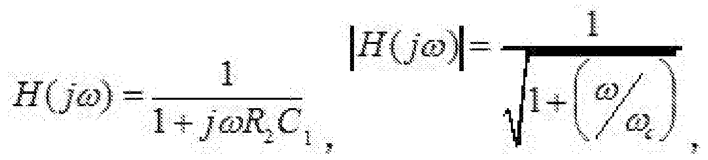
- resistors R2 and C1 form a low pass filter to filter the target pulse signal.
- any one of the signals A 0 can be expanded using Fourier series:
- Fig. 10 is a diagram showing the filtered signal of the target pulse signal, i.e., V5.
- the filtered signal at node S3 is input to the negative input of comparator CMP.
- the comparator CMP can output a digital level signal, which is a logic level signal, for example, logic 1 is a TTL high level (such as 3V), and logic 0 is a TTL low level (such as 0V).
- Figure 11 is a diagram showing the digital level signal output by the comparator.
- the comparator CMP herein may correspond to the comparison unit 422 of FIG.
- the low-pass filter composed of R2 and C1 is a comparator CMP that increases the reference voltage for comparison and can therefore be regarded as a reference voltage generating unit.
- the light receiving unit 1200 may include a phototransistor Q1 to convert an optical signal into an electrical signal.
- the photoelectric conversion unit may be used as the photoelectric conversion unit.
- the light receiving unit 1200 may further include a capacitor C1 and a resistor R1.
- the collector of the phototransistor Q1 is coupled to a power supply voltage Vcc (for example, 5V).
- Vcc for example, 5V
- the emitter of the phototransistor Q1 is coupled to one end of the resistor R1 and one end of the capacitor C1, and the other end of the resistor R1 is grounded.
- the light receiving unit 1200 may further include a voltage dividing resistor and a transistor Q2.
- the other end of the capacitor C1 is coupled to the intermediate node of the voltage dividing resistor.
- the voltage dividing resistor includes resistors R2 and R3.
- the intermediate node of R2 and R3 is also coupled to the base of transistor Q2.
- the other ends of R2 and R3 are respectively coupled to a power supply voltage Vcc and a ground.
- the emitter of transistor Q2 is grounded, and its collector is coupled to the supply voltage through resistor R4, which is also used to output the digital level signal Vout.
- the values of the voltage dividing resistors R2 and R3 determine the base voltage at the node S4.
- the base voltage is the bias voltage of the transistor Q2.
- the target optical signal of the signal source is high frequency flickering.
- the generated electrical signal on S1 is the target electrical signal corresponding to the target optical signal, which is a high and low level pulse sequence.
- the electrical signal generated at node S1 is a noisy electrical signal corresponding to ambient light when illuminated by ambient light.
- ambient light can be considered to be constant or slow to change, so the corresponding noise electrical signal can be approximated as a direct current signal.
- the electrical signal including both the target electrical signal and the noise electrical signal can be generated on the node S1.
- the electrical signal of this chirp is a pulse signal on which a DC noise electrical signal is superimposed on the basis of the target electrical signal.
- the capacitor C1 functions to conduct AC and DC. That is, the DC component in the electrical signal cannot reach node S4. As mentioned above, the noisy electrical signal is a direct current signal, or an approximately direct current signal. Thus, the capacitor C1 can effectively filter out the noise electrical signal. Therefore, C1 functions to filter the noise electrical signal, corresponding to the noise filtering unit 421 of FIG. The target pulse signal arriving at node S4 is then approximated to the target electrical signal, e.g., having a pulse sequence that is consistent with the change in the target electrical signal.
- the base voltage ⁇ can be set to be smaller than the turn-on voltage of Q2, and is larger than the turn-on voltage of Q2 after the voltage of the target pulse signal is superimposed.
- the transistor Q2 can be turned on and off regularly in accordance with the pulse sequence of the target electrical signal. By turning on and off the transistor Q2, a corresponding digital level signal Vout can be output at the collector.
- the transistor Q2 is outputted by comparing the voltage at the node S4 with its own turn-on voltage.
- the digital level signal may correspond to the comparison unit 422 of FIG. Since the reference voltage is the turn-on voltage of the transistor Q2 itself, the comparison unit 222 can be regarded as itself including the reference voltage generating unit, or the reference voltage generating unit is a part of the comparing unit.
- the light receiving unit 1300 may include a phototransistor Q1 to convert an optical signal into an electrical signal.
- the photoelectric conversion unit may be used as the photoelectric conversion unit.
- the light receiving unit 1300 may further include a capacitor C1 and a resistor R1.
- the collector of the phototransistor Q1 is coupled to a power supply voltage Vcc (for example, 5V).
- Vcc for example, 5V
- the emitter of the phototransistor Q1 is coupled to one end of the resistor R1 and one end of the capacitor C1, and the other end of the resistor R1 is grounded.
- the light receiving unit 1300 may further include a first voltage dividing resistor and a comparator CMP.
- the other end of the capacitor C 1 is coupled to the intermediate node of the voltage dividing resistor.
- the first voltage dividing resistor includes resistors R2 and R3.
- the intermediate node of R2 and R3 is also coupled to the positive input terminal of the comparator CMP.
- the other ends of R2 and R3 are respectively coupled to a power supply voltage Vc c and a ground.
- the light receiving unit 1300 may further include a second voltage dividing resistor including the resistors R4 and R5.
- the negative input terminal of the comparator CMP can be coupled to the intermediate node of the second voltage dividing resistor, and the other ends of R4 and R5 are respectively coupled to the power supply voltage Vcc and the ground.
- the circuits of Figures 13 and 12 are the same from the left until node S4, i.e., a target pulse signal can be generated at node S4.
- the difference is that the comparator CMP is used as a comparison unit in Fig. 13 to perform comparison and output. That is, the target pulse signal is input to the positive input terminal of the comparator CMP.
- the negative input terminal of the comparator CMP is coupled to the intermediate node of the second voltage dividing resistor, the junction of R4 and R5, to receive the reference voltage for comparison.
- the second voltage dividing resistor can be regarded as a reference voltage generating unit.
- the reference voltage input to the negative input terminal of the comparator CMP can be between the peak and valley of the pulse sequence of the target pulse signal.
- the CMP can output a logic level signal that reflects the digital logic of the target optical signal emitted by the signal source.
- the memory disclosed herein can be any type and size of memory and can be configured to store any type of information needed.
- various illustrative components, blocks, modules, circuits, and steps have been described above generally in the form of their function. How such functions are implemented depends on the specific application, design choices, and/or design constraints imposed on the overall system. Skilled artisans may implement the described functionality in a different manner for each particular application, and such implementation decisions should not be construed as a departure from the scope of the disclosure.
- the various illustrative logical blocks, modules, and circuits described in connection with the embodiments disclosed herein may be a processor, DSP, application specific integrated circuit (ASIC), FPGA, or other device that may be designed to perform the functions described herein. Programming logic, discrete gate or transistor logic, discrete hardware components, or any combination thereof is implemented or executed.
- the processor can be a microprocessor, but in the alternative, the processor can be any conventional processor, controller, microcontroller, or state machine.
- the processor may also be implemented as a combination of computing devices, e.g., a combination of a DSP and a microprocessor, a plurality of microprocessors, one or more microprocessors in conjunction with a DSP core, or any other such configuration.
- Embodiments disclosed herein may be implemented as hardware and instructions stored in hardware, such as may reside in random access memory (RAM), flash memory, read only memory (ROM), electricity. Programmable RO M (EPROM), electrically erasable programmable ROM (EEPROM), registers, hard disk, removable disk, CD-ROM. or any other form of storage medium known in the art.
- An exemplary storage medium is coupled to the processor to enable the processor to read/write information from/to the storage medium.
- the storage medium can be integrated into the processor.
- the processor and storage medium can reside in an ASIC.
Landscapes
- Physics & Mathematics (AREA)
- Electromagnetism (AREA)
- Engineering & Computer Science (AREA)
- Computer Networks & Wireless Communication (AREA)
- Signal Processing (AREA)
- Optical Communication System (AREA)
- Circuit Arrangement For Electric Light Sources In General (AREA)
- Light Receiving Elements (AREA)
Abstract
Description



Claims
Priority Applications (4)
| Application Number | Priority Date | Filing Date | Title |
|---|---|---|---|
| EP17762497.0A EP3429097B1 (en) | 2016-03-08 | 2017-03-03 | Optical noise removal circuit, optical receiver, and optical chip |
| KR1020187026169A KR102057726B1 (ko) | 2016-03-08 | 2017-03-03 | 조명소음 제거 회로, 수광기 및 조명칩 |
| JP2018547393A JP6955505B2 (ja) | 2016-03-08 | 2017-03-03 | 光ノイズ除去電気回路、光レシーバー及び光チップ |
| US16/122,884 US10567088B2 (en) | 2016-03-08 | 2018-09-06 | Optical noise removal circuit, optical receiver, and optical chip |
Applications Claiming Priority (4)
| Application Number | Priority Date | Filing Date | Title |
|---|---|---|---|
| CN201610131707.5 | 2016-03-08 | ||
| CN201610130395.6 | 2016-03-08 | ||
| CN201610130395.6A CN107171723B (zh) | 2016-03-08 | 2016-03-08 | 光噪去除电路以及光接收器 |
| CN201610131707.5A CN107171734B (zh) | 2016-03-08 | 2016-03-08 | 用于光通信的光芯片 |
Related Child Applications (1)
| Application Number | Title | Priority Date | Filing Date |
|---|---|---|---|
| US16/122,884 Continuation US10567088B2 (en) | 2016-03-08 | 2018-09-06 | Optical noise removal circuit, optical receiver, and optical chip |
Publications (1)
| Publication Number | Publication Date |
|---|---|
| WO2017152811A1 true WO2017152811A1 (zh) | 2017-09-14 |
Family
ID=59790030
Family Applications (1)
| Application Number | Title | Priority Date | Filing Date |
|---|---|---|---|
| PCT/CN2017/075622 Ceased WO2017152811A1 (zh) | 2016-03-08 | 2017-03-03 | 光噪去除电路、光接收器以及光芯片 |
Country Status (5)
| Country | Link |
|---|---|
| US (1) | US10567088B2 (zh) |
| EP (1) | EP3429097B1 (zh) |
| JP (1) | JP6955505B2 (zh) |
| KR (1) | KR102057726B1 (zh) |
| WO (1) | WO2017152811A1 (zh) |
Cited By (2)
| Publication number | Priority date | Publication date | Assignee | Title |
|---|---|---|---|---|
| CN110854830A (zh) * | 2018-08-20 | 2020-02-28 | 博世力士乐(西安)电子传动与控制有限公司 | 用于变频器的sto输入电路、变频器、伺服系统以及滤波泄放电路 |
| CN113075673A (zh) * | 2021-03-22 | 2021-07-06 | 深圳市德明新微电子有限公司 | 一种测距传感器及测距方法 |
Citations (6)
| Publication number | Priority date | Publication date | Assignee | Title |
|---|---|---|---|---|
| CN101232329A (zh) * | 2007-11-28 | 2008-07-30 | 华东理工大学 | 可见光通信系统的干扰消除方法 |
| CN201503272U (zh) * | 2009-10-14 | 2010-06-09 | 深圳市神舟电脑股份有限公司 | 一种滤除光噪声信号的电路 |
| KR101503519B1 (ko) * | 2012-01-18 | 2015-03-19 | 경희대학교 산학협력단 | 계층 간섭 제거 장치 및 수신 장치 |
| CN104717015A (zh) * | 2015-02-11 | 2015-06-17 | 杭州易尧数据科技有限公司 | 一种可见光通信系统、通信方法及相关设备 |
| CN104980217A (zh) * | 2015-06-19 | 2015-10-14 | 邹骁 | 一种可见光通信系统、方法及相关设备 |
| CN205407826U (zh) * | 2016-03-08 | 2016-07-27 | 深圳光启智能光子技术有限公司 | 光噪去除电路以及光接收器 |
Family Cites Families (30)
| Publication number | Priority date | Publication date | Assignee | Title |
|---|---|---|---|---|
| JPS5920299B2 (ja) * | 1978-05-17 | 1984-05-12 | 三菱電機株式会社 | 光電変換回路 |
| JPS59132264U (ja) * | 1983-02-23 | 1984-09-05 | 株式会社日立製作所 | 受光回路 |
| US5495358A (en) * | 1992-11-23 | 1996-02-27 | Hewlett-Packard Company | Optical transceiver with improved range and data communication rate |
| JPH06276157A (ja) * | 1993-03-16 | 1994-09-30 | Siemens Ag | 高速データ伝送用光受信機 |
| JP4019555B2 (ja) * | 1999-05-25 | 2007-12-12 | Kddi株式会社 | 光受信装置及び方法 |
| JP2000356676A (ja) * | 1999-06-14 | 2000-12-26 | Kenichi Suzuki | 移動体通信装置 |
| US6366373B1 (en) * | 1999-11-24 | 2002-04-02 | Luxn, Inc. | Method of intrinsic continuous management data transmission in fiber optic communications |
| AU2001237988A1 (en) * | 2000-01-26 | 2001-08-07 | Vyyo, Ltd. | Transverter control mechanism for a wireless modem in a broadband wireless access system |
| JP2002281571A (ja) * | 2001-03-22 | 2002-09-27 | Matsushita Electric Ind Co Ltd | リモートコントロール信号受信回路 |
| US6963696B1 (en) * | 2001-04-30 | 2005-11-08 | Quantum Bridge Communications, Inc. | AC-coupled burst mode receiver with wide dynamic range |
| US7309852B2 (en) * | 2004-10-18 | 2007-12-18 | Avago Technologies Ecbu Ip (Singapore) Pte Ltd. | Variable noise control for an optical transducer |
| KR100826882B1 (ko) * | 2005-12-05 | 2008-05-06 | 한국전자통신연구원 | 버스트 모드 광 수신기에서 디지털 자동이득제어 방법 및장치 |
| CN101620664A (zh) | 2008-07-03 | 2010-01-06 | 中兴通讯股份有限公司 | 一种阅读器向标签传输数据信息的方法 |
| CN101355389A (zh) * | 2008-09-11 | 2009-01-28 | 中兴通讯股份有限公司 | 一种优化调整接收机判决电平的方法及其装置 |
| JP5322120B2 (ja) * | 2008-09-19 | 2013-10-23 | 国立大学法人静岡大学 | 情報取得装置及び光通信システム |
| DE112010004476T5 (de) * | 2009-11-18 | 2012-10-04 | Taiyo Yuden Co., Ltd. | Empfangsschaltung für sichtbares Licht |
| CN102754349B (zh) * | 2010-02-19 | 2014-11-19 | 古河电气工业株式会社 | 脉冲接收机和脉冲串信号的接收方法 |
| JP2011211371A (ja) | 2010-03-29 | 2011-10-20 | Panasonic Corp | 逐次比較型ad変換器用クロック生成回路 |
| JP2011120297A (ja) * | 2011-03-03 | 2011-06-16 | Kddi Corp | データ伝送方法及びシステム、光送信装置並びに光受信装置 |
| US8464855B2 (en) * | 2011-03-21 | 2013-06-18 | Pitney Bowes Inc. | Mailing machine having optical sensors with improved immunity to ambient |
| JP2013005326A (ja) * | 2011-06-20 | 2013-01-07 | Seiwa Electric Mfg Co Ltd | 増幅回路 |
| US8559154B2 (en) * | 2011-09-01 | 2013-10-15 | Osram Sylvania Inc. | Systems and methods for switching a relay at zero cross |
| CN102594111A (zh) * | 2012-02-24 | 2012-07-18 | 中兴通讯股份有限公司 | 一种快速放电电路 |
| US20140153083A1 (en) | 2012-11-30 | 2014-06-05 | Massachusetts Institute Of Technology | Rin reduced optical source for optical coherence tomography |
| CN103812557B (zh) | 2013-07-31 | 2015-05-27 | 深圳光启创新技术有限公司 | 可见光信号的编码和解码方法、装置及系统 |
| CN105094303B (zh) | 2014-05-19 | 2018-06-29 | 深圳Tcl新技术有限公司 | 显示设备自动唤醒的方法和装置 |
| US20150372761A1 (en) * | 2014-06-23 | 2015-12-24 | Rockwell Automation Technologies, Inc. | Photoelectric sensor with tone modulation |
| CN104367309B (zh) | 2014-11-03 | 2016-09-14 | 深圳市莱通光学科技有限公司 | 一种反射式腕式心率计及反射式腕式心率测量方法 |
| CN105227245B (zh) | 2015-08-20 | 2017-10-10 | 广东顺德中山大学卡内基梅隆大学国际联合研究院 | 一种基于白光led的可见光通信系统的接收装置 |
| DE102016125457A1 (de) * | 2015-12-25 | 2017-06-29 | Panasonic Intellectual Property Management Co., Ltd. | Beleuchtungslicht-Kommunikationsvorrichtung und Kommunikationsmodul |
-
2017
- 2017-03-03 KR KR1020187026169A patent/KR102057726B1/ko not_active Expired - Fee Related
- 2017-03-03 EP EP17762497.0A patent/EP3429097B1/en not_active Not-in-force
- 2017-03-03 WO PCT/CN2017/075622 patent/WO2017152811A1/zh not_active Ceased
- 2017-03-03 JP JP2018547393A patent/JP6955505B2/ja not_active Expired - Fee Related
-
2018
- 2018-09-06 US US16/122,884 patent/US10567088B2/en not_active Expired - Fee Related
Patent Citations (6)
| Publication number | Priority date | Publication date | Assignee | Title |
|---|---|---|---|---|
| CN101232329A (zh) * | 2007-11-28 | 2008-07-30 | 华东理工大学 | 可见光通信系统的干扰消除方法 |
| CN201503272U (zh) * | 2009-10-14 | 2010-06-09 | 深圳市神舟电脑股份有限公司 | 一种滤除光噪声信号的电路 |
| KR101503519B1 (ko) * | 2012-01-18 | 2015-03-19 | 경희대학교 산학협력단 | 계층 간섭 제거 장치 및 수신 장치 |
| CN104717015A (zh) * | 2015-02-11 | 2015-06-17 | 杭州易尧数据科技有限公司 | 一种可见光通信系统、通信方法及相关设备 |
| CN104980217A (zh) * | 2015-06-19 | 2015-10-14 | 邹骁 | 一种可见光通信系统、方法及相关设备 |
| CN205407826U (zh) * | 2016-03-08 | 2016-07-27 | 深圳光启智能光子技术有限公司 | 光噪去除电路以及光接收器 |
Non-Patent Citations (1)
| Title |
|---|
| See also references of EP3429097A4 * |
Cited By (3)
| Publication number | Priority date | Publication date | Assignee | Title |
|---|---|---|---|---|
| CN110854830A (zh) * | 2018-08-20 | 2020-02-28 | 博世力士乐(西安)电子传动与控制有限公司 | 用于变频器的sto输入电路、变频器、伺服系统以及滤波泄放电路 |
| CN113075673A (zh) * | 2021-03-22 | 2021-07-06 | 深圳市德明新微电子有限公司 | 一种测距传感器及测距方法 |
| CN113075673B (zh) * | 2021-03-22 | 2024-05-03 | 深圳市德明新微电子有限公司 | 一种测距传感器及测距方法 |
Also Published As
| Publication number | Publication date |
|---|---|
| JP6955505B2 (ja) | 2021-10-27 |
| EP3429097B1 (en) | 2021-11-17 |
| US20180367221A1 (en) | 2018-12-20 |
| US10567088B2 (en) | 2020-02-18 |
| JP2019511171A (ja) | 2019-04-18 |
| EP3429097A1 (en) | 2019-01-16 |
| EP3429097A4 (en) | 2019-11-13 |
| KR102057726B1 (ko) | 2019-12-19 |
| KR20180114117A (ko) | 2018-10-17 |
Similar Documents
| Publication | Publication Date | Title |
|---|---|---|
| US8818204B2 (en) | Methods and apparatus for modulating light to concurrently convey high rate data and low rate data | |
| WO2015014160A1 (zh) | 基于多阶幅度调制的可见光信号的编码和解码方法、装置及系统 | |
| JP6058636B2 (ja) | 照明装置及び受信器 | |
| WO2017152812A1 (zh) | 用于光通信的光芯片及鉴权装置 | |
| WO2015014238A1 (zh) | 可见光信号的编码和解码方法、装置及系统 | |
| CN104869252A (zh) | 一种基于LiFi的超高速数据传输移动终端 | |
| WO2017180122A1 (en) | Optical receivers | |
| TWI616071B (zh) | 應用於可見光的可調光與光通訊之發光裝置與互動裝置 | |
| CN110771067A (zh) | 光接收装置、光发送装置、数据识别方法及多值通信系统 | |
| CN105049198B (zh) | 基于不对称的诱骗态量子密钥分发协议的通信方法 | |
| CN1082280C (zh) | 通信设备 | |
| US8402354B2 (en) | Signal processor and error correction process | |
| WO2016034036A1 (zh) | 信号的编解码方法、装置及系统 | |
| CN108880682B (zh) | 一种基于编码的可见光通信调光控制方法及系统 | |
| WO2013181980A1 (zh) | 基于可见光通信的握手同步方法和系统 | |
| WO2016034033A1 (zh) | 一种光信号编码、解码方法及装置 | |
| CN107171734B (zh) | 用于光通信的光芯片 | |
| WO2017152811A1 (zh) | 光噪去除电路、光接收器以及光芯片 | |
| WO2015014168A1 (zh) | 具有错误重发机制的可见光信号的发送方法和接收方法、装置及系统 | |
| CN205407826U (zh) | 光噪去除电路以及光接收器 | |
| CN107171723B (zh) | 光噪去除电路以及光接收器 | |
| CN103001901B (zh) | 一种基于mdpcm的集成电路高速数字接口模块 | |
| CN103812556A (zh) | 一种用于光子客户端的发光参数的调优方法 | |
| TW202433869A (zh) | 序列傳輸處理器進行近場通訊方法以及使用其之近場通訊標籤裝置 | |
| Pant et al. | Analog/Digital Data Transmission using Li-Fi |
Legal Events
| Date | Code | Title | Description |
|---|---|---|---|
| ENP | Entry into the national phase |
Ref document number: 2018547393 Country of ref document: JP Kind code of ref document: A |
|
| ENP | Entry into the national phase |
Ref document number: 20187026169 Country of ref document: KR Kind code of ref document: A |
|
| WWE | Wipo information: entry into national phase |
Ref document number: 1020187026169 Country of ref document: KR |
|
| NENP | Non-entry into the national phase |
Ref country code: DE |
|
| WWE | Wipo information: entry into national phase |
Ref document number: 2017762497 Country of ref document: EP |
|
| ENP | Entry into the national phase |
Ref document number: 2017762497 Country of ref document: EP Effective date: 20181008 |
|
| 121 | Ep: the epo has been informed by wipo that ep was designated in this application |
Ref document number: 17762497 Country of ref document: EP Kind code of ref document: A1 |