WO2017154286A1 - 素子、セル及び発電装置 - Google Patents
素子、セル及び発電装置 Download PDFInfo
- Publication number
- WO2017154286A1 WO2017154286A1 PCT/JP2016/085401 JP2016085401W WO2017154286A1 WO 2017154286 A1 WO2017154286 A1 WO 2017154286A1 JP 2016085401 W JP2016085401 W JP 2016085401W WO 2017154286 A1 WO2017154286 A1 WO 2017154286A1
- Authority
- WO
- WIPO (PCT)
- Prior art keywords
- intermediate layer
- rubber
- electrode
- electrodes
- pair
- Prior art date
- Legal status (The legal status is an assumption and is not a legal conclusion. Google has not performed a legal analysis and makes no representation as to the accuracy of the status listed.)
- Ceased
Links
Images


Classifications
-
- H—ELECTRICITY
- H10—SEMICONDUCTOR DEVICES; ELECTRIC SOLID-STATE DEVICES NOT OTHERWISE PROVIDED FOR
- H10N—ELECTRIC SOLID-STATE DEVICES NOT OTHERWISE PROVIDED FOR
- H10N30/00—Piezoelectric or electrostrictive devices
- H10N30/30—Piezoelectric or electrostrictive devices with mechanical input and electrical output, e.g. functioning as generators or sensors
-
- H—ELECTRICITY
- H02—GENERATION; CONVERSION OR DISTRIBUTION OF ELECTRIC POWER
- H02N—ELECTRIC MACHINES NOT OTHERWISE PROVIDED FOR
- H02N1/00—Electrostatic generators or motors using a solid moving electrostatic charge carrier
- H02N1/04—Friction generators
-
- H—ELECTRICITY
- H02—GENERATION; CONVERSION OR DISTRIBUTION OF ELECTRIC POWER
- H02N—ELECTRIC MACHINES NOT OTHERWISE PROVIDED FOR
- H02N11/00—Generators or motors not provided for elsewhere; Alleged perpetua mobilia obtained by electric or magnetic means
-
- H—ELECTRICITY
- H10—SEMICONDUCTOR DEVICES; ELECTRIC SOLID-STATE DEVICES NOT OTHERWISE PROVIDED FOR
- H10N—ELECTRIC SOLID-STATE DEVICES NOT OTHERWISE PROVIDED FOR
- H10N30/00—Piezoelectric or electrostrictive devices
- H10N30/50—Piezoelectric or electrostrictive devices having a stacked or multilayer structure
-
- H—ELECTRICITY
- H10—SEMICONDUCTOR DEVICES; ELECTRIC SOLID-STATE DEVICES NOT OTHERWISE PROVIDED FOR
- H10N—ELECTRIC SOLID-STATE DEVICES NOT OTHERWISE PROVIDED FOR
- H10N30/00—Piezoelectric or electrostrictive devices
- H10N30/80—Constructional details
- H10N30/85—Piezoelectric or electrostrictive active materials
- H10N30/857—Macromolecular compositions
-
- H—ELECTRICITY
- H10—SEMICONDUCTOR DEVICES; ELECTRIC SOLID-STATE DEVICES NOT OTHERWISE PROVIDED FOR
- H10N—ELECTRIC SOLID-STATE DEVICES NOT OTHERWISE PROVIDED FOR
- H10N30/00—Piezoelectric or electrostrictive devices
- H10N30/80—Constructional details
- H10N30/87—Electrodes or interconnections, e.g. leads or terminals
Definitions
- the present invention relates to an element, a cell, and a power generation device.
- vibration of structures such as roads, bridges, buildings, etc.
- vibrations of moving bodies such as automobiles and railway vehicles
- vibrations caused by human movements and wave energy and vibration energy generated by wind power are converted into electrical energy for effective use.
- Techniques to do this have been proposed.
- a piezoelectric element that can take out electricity with a relatively small external force such as rubbing the surface with a finger or the like has been disclosed (see, for example, Patent Documents 1 to 4).
- This piezoelectric element utilizes a phenomenon that charges are induced on the surface of the piezoelectric element when the piezoelectric element is strained by an external force such as vibration.
- the conventional piezoelectric element is hard, and a rigid structure is required to efficiently transmit force to the element.
- the present invention has been made in view of such a current situation, and its main object is to provide a novel element having a deformability for converting external force into electric energy.
- an element of the present invention includes a pair of electrodes, and a deformable intermediate layer that is disposed between the pair of electrodes and includes a silicon compound having an unpaired electron as a material.
- FIG. 7 It is a figure which shows an example of the whole structure of the element concerning the 1st Example of this invention. It is sectional drawing which shows an example of a structure when the element shown in FIG. 7 is made into a cell form. It is a figure which shows an example of the state which connected and arrange
- FIG. 1 is a schematic cross section of an element according to this embodiment.
- the element 1 includes a first electrode 2 and a second electrode 3 that face each other, and an intermediate layer 4 that is disposed between the first and second electrodes 2 and 3 and formed of rubber or a rubber composition. is doing.
- first electrode and second electrode There is no restriction
- the material, shape, size, and structure may be the same or different, but are preferably the same.
- the material of the first electrode 2 and the second electrode 3 include metals, carbon-based conductive materials, conductive rubber compositions, conductive polymers, and oxides.
- Examples of the metal include gold, silver, copper, aluminum, stainless steel, tantalum, nickel, and phosphor bronze.
- Examples of the carbon-based conductive material include carbon nanotubes, carbon fibers, and graphite.
- Examples of the conductive rubber composition include a composition containing a conductive filler and rubber.
- Examples of the conductive polymer include polyethylene dioxythiophene (PEDOT), polypyrrole, polyaniline, and the like.
- Examples of the oxide include indium tin oxide (ITO), indium oxide / zinc oxide (IZO), and zinc oxide.
- Examples of the conductive filler include carbon materials (for example, ketjen black, acetylene black, graphite, carbon fiber, carbon fiber (CF), carbon nanofiber (CNF), carbon nanotube (CNT), graphene, etc.), metal Filler (gold, silver, platinum, copper, aluminum, nickel, etc.), conductive polymer material (polythiophene, polyacetylene, polyaniline, polypyrrole, polyparaphenylene, and polyparaphenylene vinylene derivatives, or derivatives thereof) And the like, and ionic liquids. These may be used individually by 1 type and may use 2 or more types together.
- carbon materials for example, ketjen black, acetylene black, graphite, carbon fiber, carbon fiber (CF), carbon nanofiber (CNF), carbon nanotube (CNT), graphene, etc.
- metal Filler gold, silver, platinum, copper, aluminum, nickel, etc.
- conductive polymer material polythiophene, polyacetylene, polyaniline, polypyr
- Examples of the rubber include silicone rubber, modified silicone rubber, acrylic rubber, chloroprene rubber, polysulfide rubber, urethane rubber, butyl rubber, fluorosilicone rubber, natural rubber, ethylene / propylene rubber, nitrile rubber, fluorine rubber, isoprene rubber, Examples thereof include butadiene rubber, styrene / butadiene rubber, acrylonitrile / butadiene rubber, ethylene / propylene / diene rubber, chlorosulfonated polyethylene rubber, polyisobutylene, and modified silicone. These may be used individually by 1 type and may use 2 or more types together.
- Examples of the shape of the first electrode 2 and the shape of the second electrode 3 include a thin film.
- the structure of the first electrode 2 and the structure of the second electrode 3 may be, for example, a woven fabric, a nonwoven fabric, a knitted fabric, a mesh, a sponge, or a nonwoven fabric formed by overlapping fibrous carbon
- the average thickness of the electrode is not particularly limited and may be appropriately selected depending on the intended purpose, but is preferably 0.01 ⁇ m to 1 mm, more preferably 0.1 ⁇ m to 500 ⁇ m from the viewpoint of conductivity and flexibility. .
- the average thickness is 0.01 ⁇ m or more, the mechanical strength is appropriate and the conductivity is improved. Further, when the average thickness is 1 mm or less, the element can be deformed and the power generation performance is good.
- the intermediate layer 4 has flexibility.
- the intermediate layer 4 satisfies at least one of the following conditions (1) and (2).
- Condition (1) When the intermediate layer 4 is pressed from the direction orthogonal to the surface of the intermediate layer 4, the deformation amount of the intermediate layer 4 on the first electrode 2 side (one side), and the intermediate layer 4 The amount of deformation on the second electrode 3 side (the other side) is different.
- Condition (2) Universal hardness (H1) at the time of 10 ⁇ m indentation on the first electrode 2 side of the intermediate layer 4 and universal hardness (H2) at the time of 10 ⁇ m indentation on the second electrode 3 side of the intermediate layer 4 Different.
- the deformation amount is the maximum indentation depth of the indenter when the intermediate layer 4 is pressed under the following conditions.
- Measuring machine Microhardness tester WIN-HUD manufactured by Fischer Indenter: Square pyramid diamond indenter with a face angle of 136 °
- Initial load 0.02 mN
- Maximum load 1mN Load increase time from initial load to maximum load: 10 seconds
- the ratio (H1 / H2) of universal hardness (H1) to universal hardness (H2) is preferably 1.01 or more, more preferably 1.07 or more, and particularly preferably 1.13 or more.
- the upper limit of the ratio (H1 / H2) is not particularly limited, and is appropriately selected depending on, for example, the degree of flexibility required in the use state, the load in the use state, etc., but is preferably 1.70 or less.
- H1 is the universal hardness of the relatively hard surface
- H2 is the universal hardness of the relatively soft surface.
- middle layer 4 there is no restriction
- gum, a rubber composition, etc. are mentioned.
- rubber include silicone rubber, modified silicone rubber, acrylic rubber, chloroprene rubber, polysulfide rubber, urethane rubber, butyl rubber, fluorosilicone rubber, natural rubber, ethylene / propylene rubber, nitrile rubber, fluorine rubber, isoprene rubber, and butadiene.
- Examples thereof include rubber, styrene / butadiene rubber, acrylonitrile / butadiene rubber, ethylene / propylene / diene rubber, chlorosulfonated polyethylene rubber, polyisobutylene, and modified silicone. These may be used individually by 1 type and may use 2 or more types together. Among these, silicone rubber is preferable.
- the silicone rubber is not particularly limited as long as it is a rubber having a siloxane bond, and can be appropriately selected according to the purpose.
- the silicone rubber include dimethyl silicone rubber, methylphenyl silicone rubber, fluorosilicone rubber, and modified silicone rubber (for example, acrylic modification, alkyd modification, ester modification, and epoxy modification). These may be used individually by 1 type and may use 2 or more types together.
- the rubber composition include a composition containing a filler and the rubber. Among these, the silicone rubber composition containing the silicone rubber is preferable because of its high power generation performance.
- the filler examples include organic fillers, inorganic fillers, and organic-inorganic composite fillers.
- the organic filler is not particularly limited as long as it is an organic compound, and can be appropriately selected according to the purpose.
- examples of the organic filler include acrylic fine particles, polystyrene fine particles, melamine fine particles, fluororesin fine particles such as polytetrafluoroethylene, silicone powder (silicone resin powder, silicone rubber powder, silicone composite powder), rubber powder, wood powder, and pulp. And starch.
- silicone powder silicon resin powder, silicone rubber powder, silicone composite powder
- rubber powder wood powder, and pulp.
- starch There is no restriction
- examples of the inorganic filler include oxides, hydroxides, carbonates, sulfates, silicates, nitrides, carbons, metals, and other compounds.
- Examples of the oxide include silica, diatomaceous earth, alumina, zinc oxide, titanium oxide, iron oxide, and magnesium oxide.
- Examples of the hydroxide include aluminum hydroxide, calcium hydroxide, and magnesium hydroxide.
- Examples of the carbonate include calcium carbonate, magnesium carbonate, barium carbonate, and hydrotalcite.
- Examples of the sulfate include aluminum sulfate, calcium sulfate, and barium sulfate.
- Examples of the silicate include calcium silicate (wollastonite, zonotlite), zircon silicate, kaolin, talc, mica, zeolite, perlite, bentonite, montmoronite, sericite, activated clay, glass, hollow glass. Examples include beads.
- Examples of the nitride include aluminum nitride, silicon nitride, and boron nitride.
- Examples of the carbons include ketjen black, acetylene black, graphite, carbon fiber, carbon fiber, carbon nanofiber, carbon nanotube, fullerene (including derivatives), graphene, and the like.
- Examples of the metal include gold, silver, platinum, copper, iron, aluminum, and nickel.
- Examples of the other compounds include potassium titanate, barium titanate, strontium titanate, lead zirconate titanate, silicon carbide, molybdenum sulfide, and the like.
- the inorganic filler may be surface treated.
- the organic-inorganic composite filler can be used without particular limitation as long as it is a compound in which an organic compound and an inorganic compound are combined at a molecular level.
- examples of the organic / inorganic composite filler include silica / acryl composite fine particles and silsesquioxane.
- the average particle size of the filler is not particularly limited and may be appropriately selected depending on the intended purpose, but is preferably 0.01 ⁇ m to 30 ⁇ m, more preferably 0.1 ⁇ m to 10 ⁇ m. When the average particle size is 0.01 ⁇ m or more, the power generation performance may be improved.
- middle layer 4 can deform
- the average particle size can be measured according to a known method using a known particle size distribution measuring device such as Microtrac HRA (manufactured by Nikkiso Co., Ltd.).
- the content of the filler is preferably 0.1 to 100 parts by mass, more preferably 1 to 50 parts by mass with respect to 100 parts by mass of rubber. When the content is 0.1 parts by mass or more, power generation performance may be improved.
- middle layer 4 can deform
- limiting in particular as said other component According to the objective, it can select suitably, For example, an additive etc. are mentioned. Content of the said other component can be suitably selected in the grade which does not impair the objective of this invention.
- the additive examples include a crosslinking agent, a reaction control agent, a filler, a reinforcing material, an anti-aging agent, a conductivity control agent, a colorant, a plasticizer, a processing aid, a flame retardant, an ultraviolet absorber, and a tackifier. And thixotropic agent.
- a crosslinking agent a reaction control agent
- a filler a reinforcing material
- an anti-aging agent a conductivity control agent
- thixotropic agent There is no restriction
- the rubber composition can be prepared by mixing and kneading and dispersing the rubber, the filler, and, if necessary, the other components.
- the average thickness of the intermediate layer 4 is not particularly limited and may be appropriately selected depending on the intended purpose, but is preferably 1 ⁇ m to 10 mm, more preferably 20 ⁇ m to 1 mm from the viewpoint of deformation followability. In addition, when the average thickness is within a preferable range, film formability can be ensured and deformation is not hindered, so that good power generation can be performed.
- the intermediate layer 4 is preferably insulating.
- the insulating property preferably has a volume resistivity of 10 8 ⁇ cm or more, and more preferably has a volume resistivity of 10 10 ⁇ cm or more.
- the intermediate layer 4 may have a multilayer structure.
- Examples of the method for varying the deformation amount or hardness on both surfaces of the intermediate layer 4 include surface modification treatment and inactivation treatment. Both of these processes may be performed, or only one of them may be performed.
- ⁇ Surface modification treatment> Examples of the surface modification treatment include plasma treatment, corona discharge treatment, electron beam irradiation treatment, ultraviolet ray irradiation treatment, ozone treatment, radiation (X-ray, ⁇ -ray, ⁇ -ray, ⁇ -ray, neutron ray) irradiation treatment and the like. It is done. Among these treatments, plasma treatment, corona discharge treatment, and electron beam irradiation treatment are preferable from the viewpoint of processing speed, but are not limited to these as long as they have a certain amount of irradiation energy and can modify the material. .
- ⁇ Plasma treatment In the case of plasma processing, as the plasma generator, for example, a parallel plate type, a capacitive coupling type, an inductive coupling type, or an atmospheric pressure plasma apparatus can be used. From the viewpoint of durability, reduced pressure plasma treatment is preferred.
- the reaction pressure in the plasma treatment is not particularly limited and may be appropriately selected depending on the intended purpose, but is preferably 0.05 Pa to 100 Pa, more preferably 1 Pa to 20 Pa.
- the reaction atmosphere in the plasma treatment is not particularly limited and can be appropriately selected according to the purpose. For example, an inert gas, a rare gas, oxygen or the like is effective, but argon is effective in sustaining the effect. preferable.
- the oxygen partial pressure is preferably 5,000 ppm or less.
- production of ozone can be suppressed as the oxygen partial pressure in reaction atmosphere is 5,000 ppm or less, and use of an ozone treatment apparatus can be refrained.
- the irradiation power amount in the plasma processing is defined by (output ⁇ irradiation time).
- the irradiation power amount is preferably 5 Wh to 200 Wh, and more preferably 10 Wh to 50 Wh.
- the intermediate layer 4 can be provided with a power generation function, and durability is not reduced by excessive irradiation.
- corona discharge treatment The applied energy in corona discharge treatment (cumulative energy), preferably 6J / cm 2 ⁇ 300J / cm 2, 12J / cm 2 ⁇ 60J / cm 2 is more preferable.
- the intermediate layer 4 can be provided with a power generation function, and the durability is not reduced by excessive irradiation.
- the dose in the electron beam irradiation treatment is preferably 1 kGy or more, more preferably 300 kGy to 10 MGy.
- the intermediate layer 4 can be provided with a power generation function, and durability is not reduced by excessive irradiation.
- limiting in particular as reaction atmosphere in an electron beam irradiation process Although it can select suitably according to the objective, It fills with inert gas, such as argon, neon, helium, nitrogen, and oxygen partial pressure is 5,000 ppm or less. It is preferable that Generation
- the ultraviolet ray in the ultraviolet irradiation treatment is preferably 200 nm or more at a wavelength of 365 nm or less, and more preferably 240 nm or more at a wavelength of 320 nm or less.
- the integrated light intensity in the ultraviolet irradiation treatment preferably 5J / cm 2 ⁇ 500J / cm 2, 50J / cm 2 ⁇ 400J / cm 2 is more preferable. If the integrated light quantity is within a preferable range, the intermediate layer 4 can be provided with a power generation function, and durability is not reduced by excessive irradiation.
- reaction atmosphere in an ultraviolet irradiation process there is no restriction
- production of ozone can be suppressed as the oxygen partial pressure in reaction atmosphere is 5,000 ppm or less, and use of an ozone treatment apparatus can be refrained.
- an active group is formed by excitation or oxidation by plasma treatment, corona discharge treatment, ultraviolet irradiation treatment, electron beam irradiation treatment, etc., and the interlayer adhesion is increased.
- the technique is limited to application between layers, and application to the outermost surface has been found to be unfavorable because it rather reduces mold release.
- the reaction is performed in an oxygen-rich state, and a reactive group (hydroxyl group) is effectively introduced. Therefore, such a conventional technique is different from the surface modification treatment of the present invention.
- the surface modification treatment of the present invention promotes re-crosslinking and bonding of the surface because of treatment in a reaction environment with low oxygen and reduced pressure (for example, plasma treatment), for example, “Si—O bond with high binding energy”. Durability is improved due to "increase”. In addition, it is considered that the releasability is improved due to “densification by improving crosslinking density”.
- a part of the active group is also formed, but the active group is inactivated by a coupling agent or air drying treatment described later.
- the surface of the intermediate layer 4 may be appropriately deactivated using various materials.
- the inactivation treatment is not particularly limited as long as the surface of the intermediate layer 4 is inactivated, and can be appropriately selected according to the purpose.
- an inactivation agent is added to the intermediate layer 4.
- a treatment applied to the surface is mentioned.
- Inactivation means that the surface of the intermediate layer 4 is changed to a property that hardly causes a chemical reaction. This change is caused by reacting an active group (for example, —OH) generated by excitation or oxidation caused by plasma treatment, corona discharge treatment, ultraviolet irradiation treatment, electron beam irradiation treatment, etc. with an inactivating agent. It is obtained by reducing the surface activity.
- an active group for example, —OH
- Examples of the deactivator include an amorphous resin and a coupling agent.
- Examples of the amorphous resin include a resin having a perfluoropolyether structure in the main chain.
- Examples of the coupling agent include metal alkoxides and solutions containing metal alkoxides.
- Examples of the metal alkoxide include a compound represented by the following general formula (1), a partially hydrolyzed polycondensate having a polymerization degree of about 2 to 10, or a mixture thereof.
- R 1 (4-n) Si (OR 2 ) n General formula (1)
- R 1 and R 2 each independently represents any of a linear or branched alkyl group having 1 to 10 carbon atoms, an alkyl polyether chain, and an aryl group.
- . n represents an integer of 2 to 4.
- the inactivation treatment may be performed, for example, by impregnating the surface of the intermediate layer precursor with an inactivating agent by coating or dipping after the surface modification treatment is performed on the intermediate layer precursor such as rubber. it can.
- an inactivating agent such as silicone rubber
- after the surface modification treatment it may be deactivated by standing in the air and air drying.
- the oxygen concentration profile in the thickness direction of the intermediate layer 4 preferably has a maximum value.
- the carbon concentration profile in the thickness direction of the intermediate layer 4 preferably has a minimum value.
- the oxygen concentration profile and the carbon concentration profile can be obtained by X-ray photoelectron spectroscopy (XPS). Examples of the measurement method include the following methods.
- Measuring apparatus Ulvac-PHI Quantera SXM, manufactured by ULVAC-PHI Co., Ltd.
- Measuring light source Al (mono) Measurement output: 100 ⁇ m ⁇ , 25.1 W Measurement area: 500 ⁇ m ⁇ 300 ⁇ m Pass energy: 55 eV (narrow scan) Energy step: 0.1 eV (narrow scan)
- Relative sensitivity coefficient PHI relative sensitivity coefficient used
- XPS by capturing the electrons popping out by the photoelectron effect, it is possible to know the concentration ratio of atoms in the measurement object and the bonding state.
- Silicone rubber has a siloxane bond, and the main components are Si, O, and C. Therefore, when silicone rubber is used as the material in the intermediate layer 4, a wide scan spectrum of XPS is measured, and from the relative peak intensity ratio of each element, the existing concentration in the depth direction of each atom existing inside from the surface layer The ratio can be determined. An example is shown in FIG. Here, each atom is Si, O, and C, and the existence concentration ratio is (atomic%).
- FIG. 2 is a sample of the intermediate layer 4 obtained by using silicone rubber and further performing the surface modification treatment (plasma treatment) and the inert treatment. In FIG. 2, the horizontal axis represents the analysis depth from the surface to the inside, and the vertical axis represents the concentration ratio.
- the element bonded to silicon and the bonding state can be known by measuring the energy at which the electrons of the 2p orbit of Si jump out. Therefore, peak separation was performed from the narrow scan spectrum in the Si2p orbital indicating the Si bonding state to obtain the chemical bonding state.
- FIG. 3 is the sample used for the measurement in FIG.
- the horizontal axis is the binding energy
- the vertical axis is the intensity ratio.
- the measurement spectrum in the depth direction is shown from the bottom to the top.
- the amount of peak shift depends on the bonding state, and in the case of silicone rubber related to the present case, the peak shift to the high energy side in the Si2p orbit means that the number of oxygen bonded to Si. Indicates an increase.
- oxygen increases from the surface layer toward the inside to have a maximum value, and carbon decreases to have a minimum value. Further analysis in the depth direction causes oxygen to decrease and carbon to increase, resulting in an atomic concentration equivalent to that of untreated silicone rubber. Further, the maximum value of oxygen detected at the position of ⁇ in FIG. 2 coincides with the shift of the Si2p bond energy shift to the higher energy side (position of ⁇ in FIG. 3), and the increase in oxygen was bonded to Si. It has been shown to be due to the number of oxygen.
- FIG. 4 The results of the same analysis on the untreated silicone rubber are shown in FIG. 4 and FIG. FIG. 4 does not show the maximum value of oxygen concentration and the minimum value of carbon concentration as seen in FIG. Further, from FIG. 5, it was confirmed that the number of oxygen bonded to Si did not change because the Si2p bond energy shift did not shift to the high energy side.
- the inactivating agent soaks into the intermediate layer 4 by applying or dipping the inactivating agent such as a coupling agent to the surface of the intermediate layer 4 and allowing it to penetrate.
- the coupling agent is a compound represented by the general formula (1)
- the polyorganosiloxane is present in the intermediate layer 4 with a concentration distribution, and this distribution indicates that oxygen atoms contained in the polyorganosiloxane are present.
- the distribution has a maximum value in the depth direction.
- the intermediate layer 4 contains a polyorganosiloxane having silicon atoms bonded to 3 to 4 oxygen atoms.
- the inactivation treatment method is not limited to the dipping method.
- the intermediate layer 4 does not need to have an initial surface potential in a stationary state.
- the initial surface potential in the stationary state can be measured under the following measurement conditions.
- having no initial surface potential means ⁇ 10 V or less when measured under the following measurement conditions.
- the element 1 of the present embodiment charging by a mechanism similar to frictional charging and generation of a surface potential difference due to internal charge retention are static due to a difference in deformation based on a difference in hardness between both surfaces of the intermediate layer 4. By creating a bias in the capacitance, it is assumed that the charge moves to generate electricity.
- the element 1 preferably has a space between the intermediate layer 4 and at least one of the first electrode 2 and the second electrode 3. By doing so, the amount of power generation can be increased.
- the method of providing the space is not particularly limited and may be appropriately selected depending on the purpose. For example, a spacer is provided between the intermediate layer 4 and at least one of the first electrode 2 and the second electrode 3. And a method of arranging these.
- the material of the spacer include a polymer material, rubber, metal, a conductive polymer material, and a conductive rubber composition.
- the polymer material include polyethylene, polypropylene, polyethylene terephthalate, polyvinyl chloride, polyimide resin, fluorine resin, and acrylic resin.
- the rubber examples include silicone rubber, modified silicone rubber, acrylic rubber, chloroprene rubber, polysulfide rubber, urethane rubber, butyl rubber, fluorosilicone rubber, natural rubber, ethylene / propylene rubber, nitrile rubber, fluorine rubber, isoprene rubber, Examples thereof include butadiene rubber, styrene / butadiene rubber, acrylonitrile / butadiene rubber, ethylene / propylene / diene rubber, chlorosulfonated polyethylene rubber, polyisobutylene, and modified silicone.
- Examples of the metal include gold, silver, copper, aluminum, stainless steel, tantalum, nickel, and phosphor bronze.
- Examples of the conductive polymer material include polythiophene, polyacetylene, polyaniline, and the like.
- Examples of the conductive rubber composition include a composition containing a conductive filler and rubber.
- Examples of the conductive filler include carbon materials (eg, ketjen black, acetylene black, graphite, carbon fiber, carbon fiber, carbon nanofiber, carbon nanotube, graphene, etc.), metal (eg, gold, silver, platinum, Conductive polymer materials such as copper, iron, aluminum, nickel (eg, polythiophene, polyacetylene, polyaniline, polypyrrole, polyparaphenylene, and polyparaphenylene vinylene derivatives, or their derivatives represented by anions or cations) And the like, and ionic liquids.
- carbon materials eg, ketjen black, acetylene black, graphite, carbon fiber, carbon fiber, carbon nanofiber, carbon nanotube, graphene, etc.
- metal eg, gold, silver, platinum
- Conductive polymer materials such as copper, iron, aluminum, nickel (eg, polythiophene, polyacetylene, polyaniline, polypyrrole, polyparaphenylene, and polyparaphenylene
- Examples of the rubber include silicone rubber, modified silicone rubber, acrylic rubber, chloroprene rubber, polysulfide rubber, urethane rubber, butyl rubber, fluorosilicone rubber, natural rubber, ethylene / propylene rubber, nitrile rubber, fluorine rubber, isoprene rubber, Examples thereof include butadiene rubber, styrene / butadiene rubber, acrylonitrile / butadiene rubber, ethylene / propylene / diene rubber, chlorosulfonated polyethylene rubber, polyisobutylene, and modified silicone.
- Examples of the form of the spacer include a sheet, a film, a woven fabric, a nonwoven fabric, a mesh, and a sponge. The shape, size, thickness, and installation location of the spacer can be appropriately selected according to the structure of the element.
- the surface modification treatment or inactivation treatment is performed on the first electrode a side of the intermediate layer b. Is performed, the first electrode a side of the intermediate layer b becomes harder than the second electrode c side. Accordingly, the universal hardness is H1> H2.
- the element 1 is disposed between the first and second electrodes 2 and 3 as a pair of electrodes, and the first electrode 2 and the second electrode 3, and has deformability.
- the intermediate layer 4, the LED 30 as detection means for operation confirmation, and the rectifier circuit 40 are included.
- the element 1 also has a PET film 50 which is an exterior member formed so as to cover the first electrode 2, the second electrode 3, and the intermediate layer 4.
- the intermediate layer 4 is a rubber or rubber composition formed by subjecting a silicone rubber member to surface modification treatment by corona discharge.
- the silicone rubber member used for the intermediate layer 4 is made of silicone rubber (manufactured by Shin-Etsu Chemical Co., KE-1603) and has a film thickness of about 100 ⁇ 10 ⁇ m. That is, the intermediate layer 4 contains a silicon compound as a material. Silicone rubber members are blade-coated with silicone rubber as a material, fired at 120 ° C. for 30 minutes at high temperature, and then subjected to corona discharge treatment at an applied voltage of 100 V and an accumulated energy of 500 J / cm 2 to obtain a rectangular shape having a length of 20 mm and a width of 50 mm. It is processed into a shape.
- the intermediate layer 4 is a rubber or a rubber composition containing a silicon compound as a material.
- the intermediate layer 4 is not limited to such a configuration, and may be any material that includes a silicon compound as a material and has deformability. good.
- deformability includes flexibility and rubber elasticity, and more specifically indicates deformability to the extent that it is deformed by an external force applied by the user.
- the first electrode 2 is patterned so as to be placed on the silicone rubber member.
- the LED 30 is connected to the rectifier circuit 40 as shown in FIG.
- a voltmeter such as an oscilloscope may be disposed at the position where the LED 30 is connected.
- the first electrode 2, the second electrode 3, and the intermediate layer 4 are all covered with a PET film 50 as an exterior member and sealed with a sealing portion 51 as shown in FIG. 8A. .
- a pair of electrodes 2 and 3 and the intermediate layer 4 are covered with the exterior member and packaged, and the word “cellular” is particularly used.
- the element 1 has a function as a cell in which the element 1 and the rectifier circuit 40 are integrally formed when held in the mode shown in FIG. Further, the elements 1 may be connected and arranged side by side as shown in FIG. 8B to form one power generation element.
- Alpet 9-100 manufactured by Panac, aluminum foil thickness 9 ⁇ m, PET film thickness 100 ⁇ m
- the second electrode 3 is a continuous belt-like electrode and is disposed in contact with the intermediate layer 4.
- a spacer or the like may be disposed between the first electrode 2 or the second electrode 3 and the intermediate layer 4. According to such a configuration, the intermediate layer 4 is likely to be peeled off as described later, so that the piezoelectric effect of the element 1 is improved.
- Example 2 In place of the plasma treatment in Example 1, a UV irradiation lamp (VL-215.C manufactured by Vilver Lumat) was used, under a nitrogen atmosphere having a wavelength of 254 nm, an integrated light quantity of 300 J / cm 2 , and an oxygen partial pressure of 5000 ppm or less. Irradiation treatment was performed under conditions, and an element was produced in the same manner as in Example 1.
- VL-215.C manufactured by Vilver Lumat a UV irradiation lamp
- Example 3 Instead of the plasma treatment in Example 1, an electron beam irradiation (a line irradiation type low energy electron beam irradiation source manufactured by Hamamatsu Photonics) was used, and the irradiation treatment was performed under conditions of a nitrogen atmosphere with an irradiation dose of 1 MGy and an oxygen partial pressure of 5000 ppm or less. A device was fabricated in the same manner as in Example 1.
- an electron beam irradiation a line irradiation type low energy electron beam irradiation source manufactured by Hamamatsu Photonics
- Example 4 Regarding the fixing structure of the first electrode 2 and the second electrode 3, as shown in FIGS. 9A and 9B, the fixing layer 70 is located between the first electrode 2 and the second electrode 3, The first electrode 2 and the second electrode 3 are bonded to each other. With this configuration, when the element 1 is bent, the first electrode 2 or the second electrode 3 and the intermediate layer 4 slide relative to each other, in other words, slide.
- the first electrode 2 and the PET film 50 and the adhering respectively similarly to adhere the second electrode 3 and the PET film 50, the difference moving distance d 1 by the curvature of the flexion 10A and 10B may be configured to slide and move.
- Example 5 A rubber (Dow Corning DY35-2147 manufactured by Toray Industries, Inc.) is used as the silicone rubber member of the intermediate layer 4.
- the rubber contains iron oxide as a material, and therefore has unpaired electrons derived from iron oxide in the structure in addition to unpaired electrons derived from the silicon compound generated by the surface treatment.
- Example 1 A metal-coated piezo film sheet (200 ⁇ 280 ⁇ 110 CuNi manufactured by Tokyo Sensor) was cut into a length of 20 mm and a width of 50 mm, the metal portions of the first electrode 2 and the second electrode 3 in Example 1 were all removed by etching, and the upper and lower electrodes Were connected as shown in FIG. 8A and FIG. 8B to produce an element. That is, in this embodiment, a CuNi film covered with a piezo film sheet is used as an electrode.
- Comparative Example 2 The same metal-coated piezo film sheet as in Comparative Example 1 was etched both vertically and with a ferric chloride aqueous solution (H-200A manufactured by Sanhayato). This was put in place of the silicone rubber member of Example 1 to produce an element.
- H-200A ferric chloride aqueous solution manufactured by Sanhayato
- FIG. 4 About the structure similar to Example 1, the member which carried out the charging process of the polypropylene (PP) film substantially uniformly by corona discharge was cut into 20 mm length and 50 mm width, and was used as the intermediate
- FIG. The corona charger has a corona needle and electrode facing each other, can be discharged by a DC high-voltage power supply (HAR-20R5; manufactured by Matsusada Precision), and a grid is placed between the corona needle and the electrode. Yes. A voltage can be applied to the grid from a grid power supply different from the DC high-voltage power supply device.
- An element was fabricated using a thin film charged (electretized) under the discharge conditions shown below as the intermediate layer 4. [Charging conditions] Corona needle voltage: -10 kV Grid voltage: -1 kV The potential difference between both surfaces of the intermediate layer 4 using polypropylene was about 200V.
- Comparative Example 5 The whole polypropylene (PP) film having a thickness of 100 ⁇ m was subjected to charging treatment substantially uniformly by corona discharge in the same manner as in Comparative Example 4. Note that the potential difference between both surfaces of the intermediate layer 4 was about 200 V as in Comparative Example 4. As in Comparative Example 4, the length is set to 20 mm and the width is set to 50 mm. Instead of the silicone rubber member of Example 1, a mask pattern is used on the surface in contact with the first electrode 2 at an equal interval of about 10 mm. Then, the first electrode 2 and the intermediate layer 4 were partially point-bonded by arranging and applying in a dot shape having a diameter of about 1 mm and a thickness of 100 ⁇ m.
- Example 1 Each of the elements prepared as described above was evaluated as follows, and the results shown in Table 1 were obtained. From the results shown in Table 1, when Examples 1, 2, 3, 4, 5 and Comparative Example 2 are compared, those using the material and configuration of the present invention have high power generation performance and do not break down due to the occurrence of discharge. I can say that. In terms of durability, when Examples 1, 2, 3, 4, 5 and Comparative Example 5 are compared, those having a point adhesion structure have a low fracture durability. When Example 3 and Comparative Example 3 are compared, it can be seen that even if the same silicone rubber has no unpaired electrons, the power generation performance is not good. That is, it is considered that by treating the surface of the silicone rubber member, unpaired electrons are stably maintained as will be described later, thereby contributing to improvement in power generation performance.
- the power generation performance of the element 1 is measured using a vibration evaluator shown in FIG.
- the vibration evaluation machine is configured by combining a function generator SG-4105 (manufactured by Iwasaki Tsushinsha) and a vibration tester MES151 (manufactured by Mitsutoyo), so that both sides of the element 1 when the vibration head unit 500 moves up and down are arranged. Evaluate by voltage waveform.
- the power generating element 1 formed in a cell shape was fixed horizontally on the vibration head unit 500, and was vibrated at a vibration width of 5 mm and a vibration frequency of 10 Hz.
- the voltage waveform measured when the power generating element 1 is vibrated in this way is the voltage between the first electrode 2 and the second electrode 3, and the maximum value and the minimum value pp of the voltage are applied.
- the values are shown in Table 1.
- the pp value of the voltage of Comparative Example 1 measured in the same manner was normalized as 1, and a value of 5 times or more was determined to be a good result, and indicated in the determination column with a circle.
- the endurance test of 10,000 round trips was performed, and about the comparative example 2 with a large reduction rate, let the frequency
- ESR Electron Spin Resonance
- the g value which is a function of the magnetic field strength, is displayed on the horizontal axis, and the first derivative waveform of the absorption spectrum is displayed on the vertical axis.
- the g value is a value specific to each ESR signal determined by the frequency ( ⁇ ) of the microwave applied to the sample and the strength (H) of the resonance magnetic field.
- the ESR signal and the lattice defect are identified by the g value.
- the ESR signal is used to observe a resonance phenomenon caused by absorption of microwaves (electromagnetic wave having a frequency of about 9.4 GHz and a wavelength of about 3 cm: X band) associated with a transition of spins of unpaired electrons. Means that there are unpaired electrons in the sample. In other words, the detection of the peak of the measured waveform when taking the horizontal axis g value is equivalent to the detection of unpaired electrons.
- FIG. 13A shows the ESR signal of the intermediate layer 4 described in the third embodiment
- FIG. 13B shows the ESR signal of the intermediate layer 4 of the comparative example 3. From comparison between FIG. 13A and FIG. 13B, it is clear that the intermediate layer 4 in this embodiment has unpaired electrons.
- FIG. 13A The way of viewing FIG. 13A will be described in more detail.
- the ESR signal intensity is substantially symmetric with respect to the inversion position.
- the waveform shown in FIG. 13A is asymmetric with respect to the inversion position Q in both T1 and T2
- the intermediate layer 4 is anisotropic in structure.
- the peak value g C of the ESR signal is detected between the g values 2.070 to 2.001.
- the influence of electron thermal motion and relaxation time is reduced, so that the sensitivity of the ESR signal is improved and an ESR signal that is difficult to see in a room temperature environment is measured.
- the peak value g C not detected in the measurement result T1 is considered to indicate a peroxide radical.
- the intermediate layer 4 in the present embodiment has “at least one peak between g values of 2.004 and 1.998 when measured using an electron spin resonance apparatus”. Further, as is apparent from the measurement result T2, the intermediate layer 4 in this embodiment is “at least between g values 2.070 to 2.001 when measured at ⁇ 150 ° C. using an electron spin resonance apparatus. It has one peak ".
- ⁇ is 80% or more, ⁇ is about 30%, and no peak was detected. Those are shown in Table 1 as x.
- FIG. 10A is a schematic diagram illustrating an operation when the element 1 illustrated in FIG. 1 is bent by an external force. Due to the deformation of the element 1, the first electrode 2 or the second electrode 3 abuts on the surface of the intermediate layer 4 and moves away from or slides on the surface of the intermediate layer 4. Electron movement occurs due to work function difference.
- V represents an electromotive force generated between the first electrode 2 and the second electrode 3
- ⁇ represents a dielectric constant
- A represents an area of the element 1
- ⁇ d represents a displacement amount.
- the intermediate layer 4 may be provided with a void portion separated from one of the first electrode 2 or the second electrode 3 on the surface containing a silicon compound having unpaired electrons as a material.
- one of the first electrode 2 or the second electrode 3 and the intermediate layer 4 are likely to be deformed so as to be separated from each other, and the power generation efficiency of the element 1 is improved.
- such a deformation is not only a displacement of the element 1 in the thickness direction but also a deformation in which one of the first electrode 2 or the second electrode 3 and the intermediate layer 4 slide. May be. That is, when the element 1 is bent by an external force, the deformation may be such that at least one of the pair of electrodes and the intermediate layer 4 slide due to the difference in the moving distance d 1 caused by the curvature.
- the fixed layer 70 is fixed with insulation between the first electrode 2 and the second electrode 3, and the movement distance d caused by the curvature when the element 1 is bent by an external force. Due to the difference in 1 , at least one of the pair of electrodes and the intermediate layer 4 are fixed so as to slide. With this configuration, even when the element 1 is bent by an external force, the element 1 functions as a power generation element that converts deformation due to the external force into electrical energy.
- Example 4 at least a part of the PET film 50 and the first electrode 2 or the second electrode 3 is fixed, and due to the difference in the movement distance d 1 caused by the curvature when the element 1 is bent by an external force, At least one of the first electrode 2 or the second electrode 3 and the intermediate layer 4 slide. With this configuration, even when the element 1 is bent by an external force, the element 1 functions as a power generation element that converts deformation due to the external force into electrical energy.
- the element 1 shown in the first to fifth embodiments and the rectifier circuit 40 may be used as a power generator having the element 1 shown in the first to fifth embodiments and the rectifier circuit 40 and having a restoring force against an external force.
- the element 1 even when the element 1 is bent by an external force, the element 1 repeatedly converts deformation due to the external force into electrical energy, and thus has a function as a power generator capable of generating power continuously.
- the element shown in the above embodiment may be used not only as a power generation element but also as a sensor as a detection element that detects contact as an electric signal. Further, any other element may be used as long as it is converted from external force to electric energy.
- the effects described in the embodiments of the present invention are merely examples of the most preferable effects resulting from the present invention, and the effects of the present invention are not limited to those described in the embodiments of the present invention. .
Landscapes
- Physics & Mathematics (AREA)
- Spectroscopy & Molecular Physics (AREA)
- Laminated Bodies (AREA)
- General Electrical Machinery Utilizing Piezoelectricity, Electrostriction Or Magnetostriction (AREA)
- Treatments Of Macromolecular Shaped Articles (AREA)
- Electrostatic Charge, Transfer And Separation In Electrography (AREA)
Abstract
Description
この圧電素子は、例えば振動等の外力によって圧電素子に歪が加わる際に、圧電素子の表面に電荷が誘起される現象を利用している。
図1は、本実施形態に係る素子の模式的断面である。素子1は、互いに対向する第1の電極2及び第2の電極3と、第1及び第2の電極2,3間に配置され、ゴムまたはゴム組成物で形成された中間層4とを有している。
[第1の電極、及び第2の電極]
第1の電極2、及び第2の電極3の材質、形状、大きさ、構造としては、特に制限はなく、目的に応じて適宜選択することができる。
第1の電極2、及び第2の電極3において、その材質、形状、大きさ、構造は、同じであってもよいし、異なっていてもよいが、同じであることが好ましい。
第1の電極2、及び第2の電極3の材質としては、例えば、金属、炭素系導電材料、導電性ゴム組成物、導電性高分子、酸化物などが挙げられる。
前記導電性フィラーとしては、例えば、炭素材料(例えば、ケッチェンブラック、アセチレンブラック、黒鉛、炭素繊維、カーボンファイバー(CF)、カーボンナノファイバー(CNF)、カーボンナノチューブ(CNT)、グラフェンなど)、金属フィラー(金、銀、白金、銅、アルミニウム、ニッケルなど)、導電性高分子材料(ポリチオフェン、ポリアセチレン、ポリアニリン、ポリピロール、ポリパラフェニレン、及びポリパラフェニレンビニレンのいずれかの誘導体、又は、これら誘導体にアニオン若しくはカチオンに代表されるドーパントを添加したものなど)、イオン液体などが挙げられる。これらは、1種単独で使用してもよいし、2種以上を併用してもよい。
第1の電極2の形状、及び第2の電極3の形状としては、例えば、薄膜などが挙げられる。第1の電極2の構造、及び第2の電極3の構造としては、例えば、織物、不織布、編物、メッシュ、スポンジ、繊維状の炭素材料が重なって形成された不織布であってもよい。
中間層4は、可撓性を有する。
中間層4においては、以下の条件(1)及び条件(2)の少なくともいずれかを満たす。 条件(1):中間層4の面に対して直交する方向から中間層4が加圧された際に、中間層4における第1の電極2側(一方側)の変形量と、中間層4における第2の電極3側(他方側)の変形量とが、異なる。
条件(2):中間層4の第1の電極2側における10μm押し込み時のユニバーサル硬度(H1)と、中間層4の第2の電極3側における10μm押し込み時のユニバーサル硬度(H2)とが、異なる。
本発明において、変形量とは、以下の条件で中間層4を押し付けた際の、圧子の最大押し込み深さである。
測定機:フィッシャー社製、超微小硬度計WIN-HUD
圧子:対面角度136°の四角錐ダイヤモンド圧子
初期荷重:0.02mN
最大荷重:1mN
初期荷重から最大荷重までの荷重増加時間:10秒間
{測定条件}
測定機:フィッシャー社製、超微小硬度計WIN-HUD
圧子:対面角度136°の四角錐ダイヤモンド圧子
押し込み深さ:10μm
初期荷重:0.02mN
最大荷重:100mN
初期荷重から最大荷重までの荷重増加時間:50秒間
前記ゴム組成物としては、例えば、フィラーと前記ゴムとを含有する組成物などが挙げられる。これらの中でも、前記シリコーンゴムを含有するシリコーンゴム組成物は発電性能が高いため好ましい。
前記無機フィラーとしては、例えば、酸化物、水酸化物、炭酸塩、硫酸塩、ケイ酸塩、窒化物、炭素類、金属、又はその他の化合物などが挙げられる。
前記水酸化物としては、例えば、水酸化アルミニウム、水酸化カルシウム、水酸化マグネシウムなどが挙げられる。
前記炭酸塩としては、例えば、炭酸カルシウム、炭酸マグネシウム、炭酸バリウム、ハイドロタルサイトなどが挙げられる。
前記硫酸塩としては、例えば、硫酸アルミニウム、硫酸カルシウム、硫酸バリウムなどが挙げられる。
前記ケイ酸塩としては、例えば、ケイ酸カルシウム(ウォラストナイト、ゾノトライト)、ケイ酸ジルコン、カオリン、タルク、マイカ、ゼオライト、パーライト、ベントナイト、モンモロナイト、セリサイト、活性白土、ガラス、中空ガラスビーズなどが挙げられる。
前記炭素類としては、例えば、ケッチェンブラック、アセチレンブラック、黒鉛、炭素繊維、カーボンファイバー、カーボンナノファイバー、カーボンナノチューブ、フラーレン(誘導体を含む)、グラフェンなどが挙げられる。
前記金属としては、例えば、金、銀、白金、銅、鉄、アルミニウム、ニッケルなどが挙げられる。
前記その他の化合物としては、例えば、チタン酸カリウム、チタン酸バリウム、チタン酸ストロンチウム、チタン酸ジルコン酸鉛、炭化ケイ素、硫化モリブテン、などが挙げられる。なお、前記無機フィラーは、表面処理をしていてもよい。
前記有機無機複合フィラーとしては、例えば、シリカ・アクリル複合微粒子、シルセスキオキサンなどが挙げられる。
前記フィラーの平均粒径は、特に制限はなく、目的に応じて適宜選択することができるが、0.01μm~30μmが好ましく、0.1μm~10μmがより好ましい。前記平均粒径が、0.01μm以上であると、発電性能が向上することがある。また、前記平均粒径が、30μm以下であると、中間層4が変形可能であり、発電性能の増加を図ることができる。
前記フィラーの含有量は、ゴム100質量部に対して、0.1質量部~100質量部が好ましく、1質量部~50質量部がより好ましい。前記含有量が、0.1質量部以上であると、発電性能が向上することがある。また、前記含有量が、100質量部以下であると、中間層4が変形可能であり、発電性能の増加を図ることができる。
前記その他の成分としては、特に制限はなく、目的に応じて適宜選択することができ、例えば添加剤などが挙げられる。前記その他の成分の含有量は、本発明の目的を損なわない程度で適宜選定することができる。
前記中間層4を構成する材料の調製方法としては、特に制限はなく、目的に応じて適宜選択することができる。例えば、前記ゴム組成物の調製方法としては、前記ゴム及び前記フィラー、更に必要に応じて前記その他の成分を混合し、混錬分散することにより調製することができる。
前記中間層4の形成方法としては、特に制限はなく、目的に応じて適宜選択することができる。例えば、前記ゴム組成物の薄膜の形成方法としては、前記ゴム組成物を、基材上にブレード塗装、ダイ塗装、ディップ塗装などで塗布し、その後、熱や電子線などで硬化する方法が挙げられる。
中間層4において、両面での変形量、又は硬度を異ならせる方法としては、例えば、表面改質処理、不活性化処理などが挙げられる。これらの処理は、両方を行ってもよいし、片方のみを行ってもよい。
表面改質処理としては、例えば、プラズマ処理、コロナ放電処理、電子線照射処理、紫外線照射処理、オゾン処理、放射線(X線、α線、β線、γ線、中性子線)照射処理などが挙げられる。これらの処理の中でも、処理スピードの点から、プラズマ処理、コロナ放電処理、電子線照射処理が好ましいが、ある程度の照射エネルギーを有し、材料を改質しうるものであれば、これらに限定されない。
プラズマ処理の場合、プラズマ発生装置としては、例えば、平行平板型、容量結合型、誘導結合型のほか、大気圧プラズマ装置でも可能である。耐久性の観点から、減圧プラズマ処理が好ましい。
プラズマ処理における反応圧力としては、特に制限はなく、目的に応じて適宜選択することができるが、0.05Pa~100Paが好ましく、1Pa~20Paがより好ましい。
プラズマ処理における反応雰囲気としては、特に制限はなく、目的に応じて適宜選択することができ、例えば、不活性ガス、希ガス、酸素などのガスが有効であるが、効果の持続性においてアルゴンが好ましい。
プラズマ処理における照射電力量は、(出力×照射時間)により規定される。前記照射電力量としては、5Wh~200Whが好ましく、10Wh~50Whがより好ましい。照射電力量が、好ましい範囲内であると、中間層4に発電機能を付与でき、かつ照射過剰により耐久性を低下させることもない。
コロナ放電処理における印加エネルギー(積算エネルギー)としては、6J/cm2~300J/cm2が好ましく、12J/cm2~60J/cm2がより好ましい。印加エネルギーが、好ましい範囲内であると、中間層4に発電機能を付与でき、かつ照射過剰により耐久性を低下させることもない。
電子線照射処理における照射量としては、1kGy以上が好ましく、300kGy~10MGyがより好ましい。照射量が、好ましい範囲内であると、中間層4に発電機能を付与でき、かつ照射過剰により耐久性を低下させることもない。
電子線照射処理における反応雰囲気としては、特に制限はなく、目的に応じて適宜選択することができるが、アルゴン、ネオン、ヘリウム、窒素等の不活性ガスが充填し酸素分圧を5,000ppm以下とすることが好ましい。反応雰囲気における酸素分圧が、5,000ppm以下であると、オゾンの発生を抑制でき、オゾン処理装置の使用を控えることができる。
紫外線照射処理における紫外線としては、波長365nm以下で200nm以上が好ましく、波長320nm以下で240nm以上がより好ましい。
紫外線照射処理における積算光量としては、5J/cm2~500J/cm2が好ましく、50J/cm2~400J/cm2がより好ましい。積算光量が、好ましい範囲内であると、中間層4に発電機能を付与でき、かつ照射過剰により耐久性を低下させることもない。
さらに加えて「架橋密度向上による緻密化」に起因して離型性が向上すると考えられる。なお、本発明においても一部活性基は形成されてしまうが、後述するカップリング剤や風乾処理にて、活性基を不活性化させている。
中間層4の表面は、各種材料を用いて、適宜不活性化処理が施されてもよい。
不活性化処理としては、中間層4の表面を不活性化させる処理であれば、特に制限はなく、目的に応じて適宜選択することができ、例えば、不活性化剤を前記中間層4の表面に付与する処理が挙げられる。不活性化とは、中間層4の表面を、化学反応を起こしにくい性質に変化させることを意味する。この変化は、プラズマ処理、コロナ放電処理、紫外線照射処理、電子線照射処理などによる励起又は酸化によって発生した活性基(例えば、-OHなど)を不活性化剤と反応させて、中間層4の表面の活性度を下げることで得られる。
カップリング剤としては、例えば、金属アルコキシド、金属アルコキシドを含む溶液などが挙げられる。
R1 (4-n)Si(OR2)n・・・一般式(1)
ただし、一般式(1)中、R1及びR2は、それぞれ独立に、炭素数1~10の直鎖状又は分枝状のアルキル基、アルキルポリエーテル鎖、及びアリール基のいずれかを表す。
nは、2~4の整数を表す。
中間層前駆体としてシリコーンゴムを用いた場合は、前記表面改質処理を行った後に、空気中に静置して風乾することにより、失活させてもよい。
中間層4において、酸素濃度のプロファイルが極大値を示す位置と、炭素濃度のプロファイルが極小値を示す位置とは、一致することがより好ましい。
酸素濃度のプロファイル、及び炭素濃度のプロファイルは、X線光電子分光分析法(XPS)によって求めることができる。
測定方法は、例えば、以下の方法が挙げられる。
測定装置:Ulvac-PHI QuanteraSXM、アルバック・ファイ株式会社製
測定光源:Al(mono)
測定出力:100μmφ、25.1W
測定領域:500μm×300μm
パスエネルギー:55eV(narrow scan)
エネルギーstep:0.1eV(narrow scan)
相対感度係数:PHIの相対感度係数を使用
スパッタ源:C60クラスターイオン
Ion Gun 出力:10 kV、10 nA
Raster Control:(X=0.5,Y=2.0)mm
スパッタレート:0.9nm/min(SiO2換算)
XPSでは、光電子効果により飛び出す電子を捕捉することにより、測定対象物中の原子の存在濃度比や結合状態を知ることができる。
図2は、シリコーンゴムを用い、更に前記表面改質処理(プラズマ処理)及び前記不活性処理を行って得られた中間層4のサンプルである。図2において、横軸は表面から内部方向への分析深さであり、縦軸は存在濃度比である。
その結果を図3に示す。図3の測定対象は、図2の測定に用いたサンプルである。図3において、横軸は結合エネルギーであり、縦軸は強度比である。また、下から上に向かっては深さ方向での測定スペクトルを示している。
一般に、ピークシフトの量は結合状態に依存することが知られており、本件に関するシリコーンゴムの場合、Si2p軌道において高エネルギー側にピークがシフトするということは、Siに結合している酸素の数が増えていることを示す。
さらに図2のαの位置で検出された酸素の極大値は、Si2p結合エネルギーシフトが高エネルギー側にシフトすることと一致(図3のαの位置)しており、酸素増加がSiに結合した酸素の数に起因することが示されている。
図4には、図2にみられたような酸素濃度の極大値、及び炭素濃度の極小値は見られない。更に、図5より、Si2p結合エネルギーシフトが高エネルギー側にシフトする様子もみられないことから、Siに結合した酸素の数も変化していないことが確認された。
結果として、中間層4は、3つ~4つの酸素原子と結合したケイ素原子を有するポリオルガノシロキサンを含有することとなる。
前処理:温度30℃相対湿度40%雰囲気に24h静置後、除電を60sec(Keyence製のSJ-F300を使用)
装置:Treck Model344
測定プローブ:6000B-7C
測定距離:2mm
測定スポット径:直径10mm
素子1は、中間層4と、第1の電極2及び第2の電極3の少なくともいずれかとの間に空間を有することが好ましい。そうすることにより、発電量を増やすことができる。
前記空間を設ける方法としては、特に制限はなく、目的に応じて適宜選択することができ、例えば、中間層4と、第1の電極2及び第2の電極3の少なくともいずれかとの間にスペーサを配置する方法などが挙げられる。
前記高分子材料としては、例えば、ポリエチレン、ポリプロピレン、ポリエチレンテレフタレート、ポリ塩化ビニル、ポリイミド樹脂、フッ素樹脂、アクリル樹脂などが挙げられる。前記ゴムとしては、例えば、シリコーンゴム、変性シリコーンゴム、アクリルゴム、クロロプレンゴム、多硫化ゴム、ウレタンゴム、ブチルゴム、フロロシリコーンゴム、天然ゴム、エチレン・プロピレンゴム、ニトリルゴム、フッ素ゴム、イソプレンゴム、ブタジエンゴム、スチレン・ブタジエンゴム、アクリロニトリル・ブタジエンゴム、エチレン・プロピレン・ジエンゴム、クロロスルホン化ポリエチレンゴム、ポリイソブチレン、変成シリコーンなどが挙げられる。
前記スペーサの形態としては、例えば、シート、フィルム、織布、不織布、メッシュ、スポンジなどが挙げられる。
前記スペーサの形状、大きさ、厚み、設置場所は、素子の構造に応じて適宜選択することができる。
これにより、同じ変形付与力である加圧力Fが第1の電極a側と第2の電極c側に作用した場合、中間層bの第1の電極a側の変形の度合いが、第2の電極c側よりも小さくなる。
素子1は、図7に示すように、一対の電極としての第1及び第2の電極2,3と、第1の電極2と第2の電極3との間に配置され、変形性を備えた中間層4と、動作確認のための検知手段たるLED30と、整流回路40と、を有している。
素子1はまた、第1の電極2と、第2の電極3と、中間層4とを覆うように形成された外装部材たるPETフィルム50を有している。
中間層4に用いるシリコーンゴム部材は、シリコーンゴム(信越化学製、KE-1603)を用いており、膜厚は約100±10μmである。すなわち、中間層4は、ケイ素化合物を材料として含んでいる。
シリコーンゴム部材は、材料となるシリコーンゴムをブレード塗装し、30分、120℃で高温焼成した後、印加電圧100V、積算エネルギー500J/cm2でコロナ放電処理を行い、縦20mm、横50mmの矩形状に加工したものである。
なおここでは中間層4は、ケイ素化合物を材料として含むゴムまたはゴム組成物であるとしたが、かかる構成に限定されるものではなく、ケイ素化合物を材料として含み、変形性を備えるものであれば良い。かかる変形性とは、可撓性及びゴム弾性を含み、より詳しくは使用者が印加する外力によって変形する程度の変形性を示している。
LED30は、図7に示すように整流回路40と結線されて、整流回路40の通電を検知して点灯する。なお、以降の説明において、素子1の電極間に生じる電圧または中間層4の上下面間の電圧を測定する必要があるときには、LED30の接続された位置にオシロスコープなどの電圧計を配置すると良い。
第1の電極2と、第2の電極3と、中間層4とは、図8Aに示すように何れも外装部材としてのPETフィルム50に覆われて、封止部51によって封止されている。このように一対の電極2,3と、中間層4とが外装部材によって覆われ、パッケージングされた状態を指して、特に「セル状」との文言を用いる。すなわち、素子1は、図7に示す態様で保持されるとき、素子1と整流回路40とが一体に形成されたセルとしての機能を有している。また、素子1を図8Bに示すように連結して並べて配置し、1つの発電素子としても良い。
第2の電極3は、連続した帯状の電極であり、中間層4と当接して配置されている。
なお、第1の電極2または第2の電極3と、中間層4と、の間には、スペーサーなどを配置しても良い。かかる構成によれば、中間層4が後述するように剥離帯電が生じやすくなることにより、素子1の圧電効果が向上する。
実施例1におけるプラズマ処理の代わりに、UV照射ランプ(ヴィルヴァー・ルーマット社製VL-215.C)を用いて、波長254nm、積算光量300J/cm2、酸素分圧5000ppm以下の窒素雰囲気下の条件で照射処理を行い、実施例1と同様に素子を作成した。
実施例1におけるプラズマ処理の代わりに、電子線照射(浜松ホトニクス社製ライン照射型低エネルギー電子線照射源)を用いて、照射量1MGy、酸素分圧5000ppm以下の窒素雰囲気下の条件で照射処理を行い、実施例1と同様に素子を作成した。
第1の電極2と第2の電極3との固定構造について、図9Aおよび図9Bに示すように、固定層70が第1の電極2と第2の電極3との間に位置し、第1の電極2と第2の電極3とを互いに接着している。
かかる構成により、素子1を屈曲させたときに、第1の電極2または第2の電極3と、中間層4とが互いに滑り移動、言い換えると摺動する。あるいは、この構成例は、第1の電極2とPETフィルム50とをそれぞれ接着し、同様に第2の電極3とPETフィルム50とを接着して、屈曲時の曲率による移動距離d1の違いで滑り移動する図10Aおよび図10Bのような構成であっても良い。
中間層4のシリコーンゴム部材としてゴム(東レ製ダウコーニングDY35-2147)を用いたものである。当該ゴムは、酸化鉄を材料として含んでおり、したがって表面処理によって生じるケイ素化合物由来の不対電子の他に、酸化鉄由来の不対電子をも構造中に有している。
金属被覆ピエゾフィルムシート(東京センサー製200×280×110CuNi)を縦20mm横50mmに切り出し、実施例1における第1の電極2と第2の電極3の金属部分をすべてエッチングで取り除き、上下の電極を図8Aおよび図8Bに示すように結線して素子を作成した。
すなわち、本実施形態では、ピエゾフィルムシートに被覆されているCuNi膜を電極として用いている。
比較例1と同様の金属被覆ピエゾフィルムシートを塩化第2鉄水溶液(サンハヤト製H-200A)で上下ともすべてエッチングした。これを実施例1のシリコーンゴム部材の代わりに入れ、素子を作成した。
実施例1のシリコーンゴムで、表面処理をしないものを使用して素子を作成した。
実施例1と同様の構成について、ポリプロピレン(PP)フィルムを、コロナ放電によって全体を略均一に帯電処理を行った部材を縦20mm横50mmに切り分けて中間層4として用いた。コロナ帯電器はコロナ針と電極とが対向配置され、直流高圧電源装置(HAR-20R5;松定プレシジョン製)により、放電が可能となっており、更にコロナ針と電極間にグリッドが配置されている。グリッドには直流高圧電源装置とは異なるグリッド用電源から電圧を印加できる。下記に示す放電条件で帯電(エレクトレット化)した薄膜を中間層4として用いて素子を作成した。
[帯電条件]
コロナ針電圧:-10kV
グリッド電圧:-1kV
なお、ポリプロピレンを用いた中間層4の両表面間の電位差は約200Vであった。
厚さ100μmのポリプロピレン(PP)フィルム全体を、比較例4と同様に、コロナ放電によって略均一に帯電処理を行ったものを用いた。なお、中間層4の両表面間の電位差は、比較例4と同様に約200Vであった。
比較例4と同様に縦20mm横50mmとし、実施例1のシリコーンゴム部材の代わりに入れ、第1の電極2と当接する側の面に、接着剤を約10mmの等間隔でマスクパターンを用いて直径約1mm、厚み100μmのドット状に配列塗布することによって、第1の電極2と中間層4とを部分的にポイント接着した。
また、耐久性能でみた場合、実施例1、2、3、4、5と比較例5を比較するとポイント接着構造を持ったものは、破壊耐久性が小さい。
実施例3と比較例3とを比較すると、同じシリコーンゴムであっても不対電子のないものは、発電性能がよくないことが分かる。すなわち、シリコーンゴム部材を表面処理することで、後述するように不対電子が安定的に維持されて発電性向上に寄与していると考えられる。
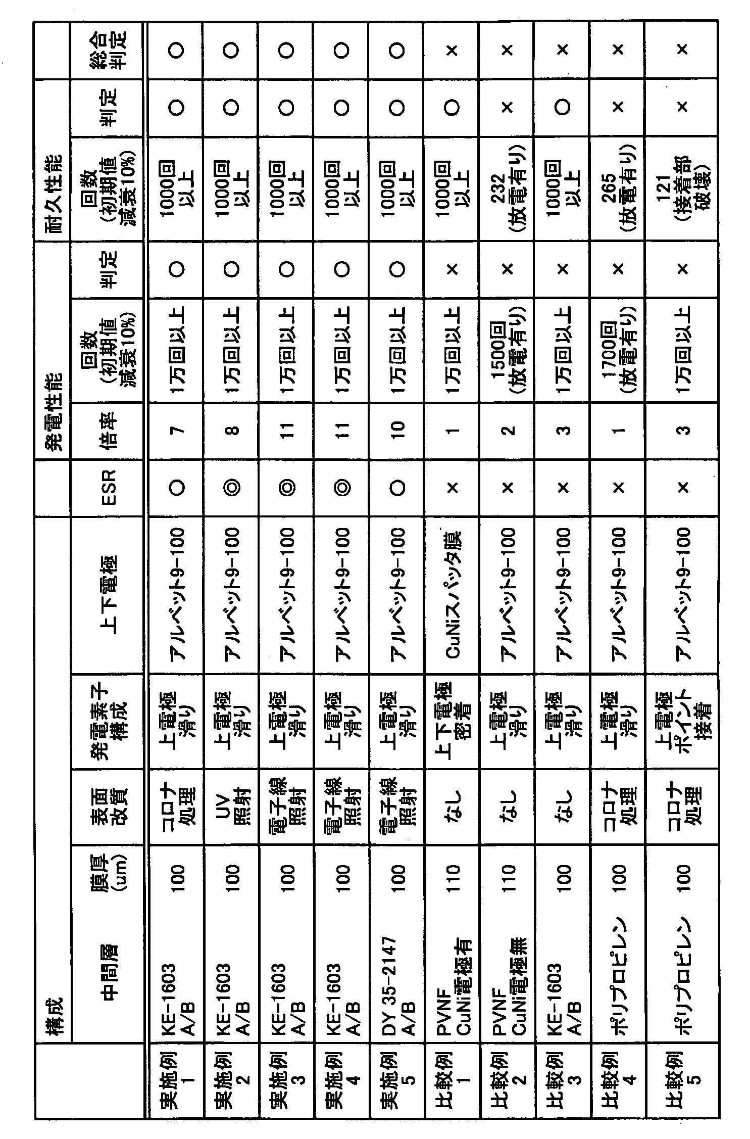
素子1の発電性能を図11に示す振動評価機を用いて測定する。
振動評価機は、ファンクションジェネレータSG-4105(岩崎通信社製)と、振動試験機MES151(Mitsutoyo製)と、が組み合わせて構成され、加振ヘッド部500が上下動するときの素子1の両面の電圧波形によって評価を行う。
加振ヘッド部500にセル状に形成した発電素子1を水平に固定し、振動幅5mm、振動周波数10Hzにて加振した。
また、評価の基準としては、同様に測定した比較例1の電圧のp-p値を1として規格化し、5倍以上のものを良好な成績と判定し、判定欄に○で表記した。
以上の測定について、5サンプルの平均値をとるとともに、往復1万回の耐久試験を行い、減少率が大きかった比較例2については、初期値から10%減になった回数を「回数」として示した。
セル状に形成した素子1の曲げ耐久性能を測定するために、卓上型耐久試験機TCDM111LH(ユアサシステム機器製)を用いて図12Aおよび図12Bに示すように、90°の屈曲試験を行った。
R30の治具の中間にサンプルを設置し、毎分10往復、1000回の耐久試験を行い、電圧のp-p値の測定を行った。
評価1と同様に、初期値から10%減になったものは、その回数を回数の欄に記載した。
中間層4の材料評価試験として、XバンドESR測定装置EMX-nano(Bruker製)を用いて測定した。かかる測定結果について、環境温度が室温の場合の測定結果T1を破線で、環境温度が-150℃の場合の測定結果T2を実線で、それぞれ図13Aに示した。同様に、比較例3の中間層4を用いてESR測定を行った結果について図13Bに示した。
ESR信号は、不対電子のスピンの遷移に伴うマイクロ波(周波数9.4GHz、波長3cm程度の電磁波:Xバンド)の吸収による共鳴現象を観測するものであるから、ESR信号が検出されることは、試料内に不対電子が存在することを意味している。言い換えると、横軸g値に取ったときの測定波形のピークが検出されることは、不対電子が検出されたことと等しい。
また、測定結果T1、T2に表示されるESR信号のピーク値gA、gBは、何れも、石英ガラス中の欠損で測定されるE’センターg⊥(=2.0014)と、E’センターg∥(=2.0004)によく一致している。
このことは、表面処理によってシリコーンゴム中に酸素Oの欠損が生じ、当該欠損位置に不対電子が形成されていることを示していると考えられる。
したがって、本実施形態における中間層4が測定結果T1において、g値2.004~1.998の間に2つのピークを有することは、中間層4の厚み方向に、異方性を有していることを示していると考えられる。
一般に、-150℃での低温測定では、電子の熱運動や緩和時間の影響が小さくなるため、ESR信号の感度が向上し、室温環境では見ることの難しいESR信号が測定される。
測定結果T2において、測定結果T1には検出されていないピーク値gCは、過酸化ラジカルを示すものであると考えられる。
また、測定結果T2から明らかなように、本実施形態における中間層4は、「電子スピン共鳴装置を用いて-150℃において測定されるとき、g値2.070~2.001の間に少なくとも1つのピークを有し」ている。
図10Aは、図1に示した素子1が、外力によって撓められた場合の動作について示す模式図である。
素子1の変形によって、第1の電極2または第2の電極3が中間層4の表面に当接し、離間するあるいは摺動することで、電極部分の金属と、中間層4との間の表面仕事関数差によって、電子の移動が生じる。
特に、中間層4がゴム弾性を有する場合には、かかる変形による当接と離間とが繰り返し生じやすく、大きな帯電量を得られる。
かかる帯電によって、中間層4がコンデンサのような役割を果たし、V=Q/C=(Q×Δd)/(ε×A)の起電力が生じる。なお、ここでVは第1の電極2と第2の電極3との間に生じる起電力、εは誘電率、Aは素子1の面積、Δdは変位量をそれぞれ示している。
かかる構成により素子1は、外力による変形を電気的なエネルギーへと変換する発電素子として機能している。
ところで、このような変形については、素子1の厚さ方向への変位のみならず、第1の電極2あるいは第2の電極3の一方と、中間層4とが摺動するような変形であっても良い。すなわち、素子1が外力により屈曲したときに、曲率によって生じる移動距離d1の違いにより、一対の電極の少なくとも一方と、中間層4とが摺動する変形であっても良い。
かかる構成により、素子1が外力によって屈曲したときにも、素子1は外力による変形を電気的なエネルギーへと変換する発電素子として機能する。
かかる構成により、素子1が外力によって屈曲したときにも、素子1は外力による変形を電気的なエネルギーへと変換する発電素子として機能する。
かかる構成により、素子1が外力によって屈曲したときにも、素子1は外力による変形を繰り返し電気的なエネルギーへと変換するから、持続的に発電可能な発電装置としての機能を有する。
本発明実施の形態に記載された効果は、本発明から生じる最も好適な効果を例示したに過ぎず、本発明による効果は、本発明の実施形態に記載されたものに限定されるものではない。
2 一対の電極(第1の電極)
3 一対の電極(第2の電極)
4 中間層
40 整流回路
50 外装部材(PETフィルム)
51 封止部
70 固定構造(固定層)
Claims (9)
- 一対の電極と、
前記一対の電極の間に配置され、不対電子を有するケイ素化合物を材料として含む変形性を備えた中間層と、
を、有することを特徴とする素子。 - 請求項1に記載の素子であって、
前記中間層が不対電子を持つ粒子を含むことを特徴とする素子。 - 請求項1に記載の素子であって、
前記中間層は、ゴム弾性を有することを特徴とする素子。 - 請求項1に記載の素子であって、
前記中間層は、電子スピン共鳴(ESR)装置を用いて測定されるとき、g値2.004~1.998の間に少なくとも1つのピークを有することを特徴とする素子。 - 請求項1に記載の素子であって、
前記中間層は、電子スピン共鳴(ESR)装置を用いて-150℃の環境温度下で測定されるとき、g値2.070~2.001の間に少なくとも1つのピークを持つことを特徴とする素子。 - 請求項1に記載の素子であって、
前記一対の電極の一部は、当該電極間で絶縁性を有したまま固定する固定構造を有し、
前記固定構造は、前記素子が外力により屈曲したときに、曲率によって生じる移動距離の違いにより、前記一対の電極の少なくとも一方と、前記中間層とが摺動するように前記一対の電極を固定することを特徴とする素子。 - 請求項1に記載の素子と、
前記一対の電極と前記中間層とを覆う可撓性のある外装部材と、
を有するセル。 - 請求項7に記載のセルであって、
前記外装部材と前記電極の少なくとも一部を固定するための固定構造を有し、
前記固定構造は、当該セルが外力により屈曲したときに曲率によって生じる移動距離の違いにより、前記一対の電極の少なくとも一方と、前記中間層とが摺動するように前記一対の電極と前記外装部材とを固定することを特徴とするセル。 - 請求項7に記載のセルと、
整流回路とを有し、外力に対して復元力を有することを特徴とする発電装置。
Priority Applications (5)
| Application Number | Priority Date | Filing Date | Title |
|---|---|---|---|
| KR1020187024752A KR102115870B1 (ko) | 2016-03-07 | 2016-11-29 | 소자, 셀, 및 발전 디바이스 |
| US16/080,993 US11189778B2 (en) | 2016-03-07 | 2016-11-29 | Element, cell, and power generation device |
| EP16893610.2A EP3429075B1 (en) | 2016-03-07 | 2016-11-29 | Element, cell, and power generation device |
| JP2018504001A JP6658864B2 (ja) | 2016-03-07 | 2016-11-29 | 素子、セル及び発電装置 |
| CN201680083253.7A CN108702108B (zh) | 2016-03-07 | 2016-11-29 | 元件、电池、和发电装置 |
Applications Claiming Priority (2)
| Application Number | Priority Date | Filing Date | Title |
|---|---|---|---|
| JP2016-043657 | 2016-03-07 | ||
| JP2016043657 | 2016-03-07 |
Publications (1)
| Publication Number | Publication Date |
|---|---|
| WO2017154286A1 true WO2017154286A1 (ja) | 2017-09-14 |
Family
ID=59790177
Family Applications (1)
| Application Number | Title | Priority Date | Filing Date |
|---|---|---|---|
| PCT/JP2016/085401 Ceased WO2017154286A1 (ja) | 2016-03-07 | 2016-11-29 | 素子、セル及び発電装置 |
Country Status (6)
| Country | Link |
|---|---|
| US (1) | US11189778B2 (ja) |
| EP (1) | EP3429075B1 (ja) |
| JP (1) | JP6658864B2 (ja) |
| KR (1) | KR102115870B1 (ja) |
| CN (1) | CN108702108B (ja) |
| WO (1) | WO2017154286A1 (ja) |
Cited By (2)
| Publication number | Priority date | Publication date | Assignee | Title |
|---|---|---|---|---|
| JP2021064690A (ja) * | 2019-10-11 | 2021-04-22 | 株式会社リコー | 素子および素子の製造方法 |
| JP2021158215A (ja) * | 2020-03-26 | 2021-10-07 | 三菱ケミカル株式会社 | 積層圧電シート |
Families Citing this family (10)
| Publication number | Priority date | Publication date | Assignee | Title |
|---|---|---|---|---|
| JP6870200B2 (ja) * | 2014-11-13 | 2021-05-12 | 株式会社リコー | 素子、及び発電装置 |
| CN108885146B (zh) * | 2016-01-29 | 2020-12-18 | 株式会社理光 | 压敏传感器,抓取装置和机器人 |
| WO2018101359A1 (ja) * | 2016-11-30 | 2018-06-07 | 株式会社ユポ・コーポレーション | 圧電素子および楽器 |
| GB201707486D0 (en) * | 2017-05-10 | 2017-06-21 | Univ Bristol | Radiation powered devices comprising diamond material |
| DE102018221053A1 (de) * | 2018-04-05 | 2019-10-10 | Continental Reifen Deutschland Gmbh | Vorrichtung zum Messen einer mechanischen Kraft, umfassend eine erste, zweite, dritte, vierte und fünfte Schicht sowie die Verwendungen der Vorrichtung und Reifen oder technischer Gummiartikel umfassend die Vorrichtung |
| KR102143112B1 (ko) * | 2018-09-04 | 2020-08-10 | 한국과학기술연구원 | 복합체 액추에이터 장치 |
| US12056994B2 (en) * | 2020-07-15 | 2024-08-06 | Xerox Corporation | Systems and methods for improved object placement sensing for point-of-purchase sales |
| US12216011B2 (en) | 2020-07-30 | 2025-02-04 | Xerox Corporation | Systems and methods for improved sensing performance of pressure-sensitive conductive sheets |
| CN112928944B (zh) * | 2021-01-25 | 2022-09-16 | 江苏大学 | 一种基于摩擦纳米发电机的波浪能发电装置 |
| US12009159B2 (en) | 2021-04-13 | 2024-06-11 | Xerox Corporation | Membrane switches configured to sense pressure applied from compliant and rigid objects |
Citations (5)
| Publication number | Priority date | Publication date | Assignee | Title |
|---|---|---|---|---|
| JP2004120809A (ja) * | 2002-09-24 | 2004-04-15 | Ricoh Co Ltd | 無機エレクトレットアクチュエータ及びその製造方法、液滴吐出ヘッド、光学デバイス、圧力センサ、発振器、モータ |
| WO2013157643A1 (ja) * | 2012-04-20 | 2013-10-24 | 旭化成イーマテリアルズ株式会社 | ラジカル架橋性基を有するポリシロキサン組成物 |
| JP2014220949A (ja) * | 2013-05-09 | 2014-11-20 | バンドー化学株式会社 | アクチュエータ素子、アクチュエータ、可撓性シート及びアクチュエータ素子の製造方法 |
| JP5699641B2 (ja) * | 2011-01-31 | 2015-04-15 | 大日本印刷株式会社 | 積層体およびその製造方法 |
| JP2015122922A (ja) * | 2013-12-25 | 2015-07-02 | 株式会社ビスキャス | 振動発電体 |
Family Cites Families (25)
| Publication number | Priority date | Publication date | Assignee | Title |
|---|---|---|---|---|
| SE347356B (ja) | 1970-03-20 | 1972-07-31 | Essem Metotest Ab | |
| US5376590A (en) * | 1992-01-20 | 1994-12-27 | Nippon Telegraph And Telephone Corporation | Semiconductor device and method of fabricating the same |
| US5699641A (en) | 1996-02-23 | 1997-12-23 | Usg Interiors, Inc. | Suspension ceiling with integrated openings |
| JP2002075987A (ja) | 2000-08-25 | 2002-03-15 | Toyota Central Res & Dev Lab Inc | 半導体装置の製造方法 |
| JP3694740B2 (ja) | 2001-03-08 | 2005-09-14 | 独立行政法人産業技術総合研究所 | 薄型圧力センサ及びそれを用いた人体情報計測装置 |
| US6823739B2 (en) | 2001-12-20 | 2004-11-30 | National Institute Of Advanced Industrial Science And Technology | Thin pressure sensor and biological information measuring device using same, and biological information measuring method |
| JP2006278583A (ja) * | 2005-03-28 | 2006-10-12 | Dainippon Printing Co Ltd | 有機薄膜太陽電池 |
| JP2009232677A (ja) | 2008-02-25 | 2009-10-08 | Nsk Ltd | エラストマートランスデューサーおよび誘電性ゴム組成物ならびに発電素子 |
| JP2011049073A (ja) | 2009-08-27 | 2011-03-10 | Nsk Ltd | 発電素子 |
| TWI538218B (zh) * | 2010-09-14 | 2016-06-11 | 半導體能源研究所股份有限公司 | 薄膜電晶體 |
| GB201016193D0 (en) * | 2010-09-27 | 2010-11-10 | Univ Bolton | Hybrid energy conversion device |
| WO2012046560A1 (en) * | 2010-10-04 | 2012-04-12 | Semiconductor Energy Laboratory Co., Ltd. | Composite material, light-emitting element, light-emitting device, electronic device, and lighting device |
| CN103339715B (zh) * | 2010-12-03 | 2016-01-13 | 株式会社半导体能源研究所 | 氧化物半导体膜以及半导体装置 |
| JP5691080B2 (ja) | 2012-07-25 | 2015-04-01 | 株式会社ビスキャス | 振動発電体およびその製造方法と発電方法 |
| KR101868780B1 (ko) * | 2012-12-28 | 2018-06-20 | 다우 코닝 도레이 캄파니 리미티드 | 변환기용 경화성 유기폴리실록산 조성물 및 그러한 변환기용 경화성 실리콘 조성물의 응용 |
| CN103354429B (zh) | 2013-03-12 | 2015-09-16 | 北京纳米能源与系统研究所 | 一种滑动摩擦纳米发电机及发电方法 |
| CN103368453B (zh) | 2013-03-12 | 2016-04-13 | 北京纳米能源与系统研究所 | 一种滑动摩擦纳米发电机及发电方法 |
| CN104135186A (zh) | 2013-05-03 | 2014-11-05 | 纳米新能源(唐山)有限责任公司 | 悬臂梁结构式摩擦发电机和发电机组 |
| CN104283453B (zh) | 2013-07-11 | 2017-02-15 | 北京纳米能源与系统研究所 | 滑动摩擦发电机、发电方法以及矢量位移传感器 |
| CN104426414B (zh) * | 2013-08-23 | 2016-08-10 | 纳米新能源(唐山)有限责任公司 | 发电效果改善的摩擦发电机及其制备方法 |
| JP2015198154A (ja) | 2014-04-01 | 2015-11-09 | 帝人株式会社 | 圧電素子 |
| US20160088696A1 (en) | 2014-09-19 | 2016-03-24 | Osamu Kizaki | System for controlling control target units, method of controlling control target units, and recording medium |
| US20160088706A1 (en) | 2014-09-19 | 2016-03-24 | Osamu Kizaki | Detection device, detection method, and recording medium storing a detection program |
| JP6699119B2 (ja) | 2015-01-22 | 2020-05-27 | 株式会社リコー | 素子及び発電装置 |
| JP6618035B2 (ja) | 2015-03-09 | 2019-12-11 | 株式会社リコー | 素子、及び発電装置 |
-
2016
- 2016-11-29 WO PCT/JP2016/085401 patent/WO2017154286A1/ja not_active Ceased
- 2016-11-29 CN CN201680083253.7A patent/CN108702108B/zh active Active
- 2016-11-29 JP JP2018504001A patent/JP6658864B2/ja active Active
- 2016-11-29 EP EP16893610.2A patent/EP3429075B1/en active Active
- 2016-11-29 KR KR1020187024752A patent/KR102115870B1/ko active Active
- 2016-11-29 US US16/080,993 patent/US11189778B2/en active Active
Patent Citations (5)
| Publication number | Priority date | Publication date | Assignee | Title |
|---|---|---|---|---|
| JP2004120809A (ja) * | 2002-09-24 | 2004-04-15 | Ricoh Co Ltd | 無機エレクトレットアクチュエータ及びその製造方法、液滴吐出ヘッド、光学デバイス、圧力センサ、発振器、モータ |
| JP5699641B2 (ja) * | 2011-01-31 | 2015-04-15 | 大日本印刷株式会社 | 積層体およびその製造方法 |
| WO2013157643A1 (ja) * | 2012-04-20 | 2013-10-24 | 旭化成イーマテリアルズ株式会社 | ラジカル架橋性基を有するポリシロキサン組成物 |
| JP2014220949A (ja) * | 2013-05-09 | 2014-11-20 | バンドー化学株式会社 | アクチュエータ素子、アクチュエータ、可撓性シート及びアクチュエータ素子の製造方法 |
| JP2015122922A (ja) * | 2013-12-25 | 2015-07-02 | 株式会社ビスキャス | 振動発電体 |
Non-Patent Citations (1)
| Title |
|---|
| See also references of EP3429075A4 * |
Cited By (3)
| Publication number | Priority date | Publication date | Assignee | Title |
|---|---|---|---|---|
| JP2021064690A (ja) * | 2019-10-11 | 2021-04-22 | 株式会社リコー | 素子および素子の製造方法 |
| JP2021158215A (ja) * | 2020-03-26 | 2021-10-07 | 三菱ケミカル株式会社 | 積層圧電シート |
| JP7491013B2 (ja) | 2020-03-26 | 2024-05-28 | 三菱ケミカル株式会社 | 積層圧電シート |
Also Published As
| Publication number | Publication date |
|---|---|
| JP6658864B2 (ja) | 2020-03-04 |
| EP3429075B1 (en) | 2020-10-28 |
| US11189778B2 (en) | 2021-11-30 |
| JPWO2017154286A1 (ja) | 2018-10-04 |
| EP3429075A1 (en) | 2019-01-16 |
| KR102115870B1 (ko) | 2020-05-28 |
| US20190103548A1 (en) | 2019-04-04 |
| EP3429075A4 (en) | 2019-02-27 |
| KR20180107190A (ko) | 2018-10-01 |
| CN108702108A (zh) | 2018-10-23 |
| CN108702108B (zh) | 2020-04-14 |
Similar Documents
| Publication | Publication Date | Title |
|---|---|---|
| JP6658864B2 (ja) | 素子、セル及び発電装置 | |
| JP6801188B2 (ja) | 発電素子及び発電装置 | |
| JP6870200B2 (ja) | 素子、及び発電装置 | |
| EP3070833B1 (en) | Electric generating element and electric generator | |
| US10714676B2 (en) | Sensor and sensor system | |
| JP6672817B2 (ja) | 素子 | |
| JP2017108596A (ja) | 発電装置 | |
| JP2017099105A (ja) | 発電装置 | |
| JP6808930B2 (ja) | 発電素子及び発電装置 | |
| JP2018087801A (ja) | センサ及びセンサシステム | |
| EP3806315B1 (en) | Element and method for manufacturing element | |
| EP4064300A1 (en) | Element |
Legal Events
| Date | Code | Title | Description |
|---|---|---|---|
| ENP | Entry into the national phase |
Ref document number: 2018504001 Country of ref document: JP Kind code of ref document: A |
|
| ENP | Entry into the national phase |
Ref document number: 20187024752 Country of ref document: KR Kind code of ref document: A |
|
| NENP | Non-entry into the national phase |
Ref country code: DE |
|
| WWE | Wipo information: entry into national phase |
Ref document number: 2016893610 Country of ref document: EP |
|
| ENP | Entry into the national phase |
Ref document number: 2016893610 Country of ref document: EP Effective date: 20181008 |
|
| 121 | Ep: the epo has been informed by wipo that ep was designated in this application |
Ref document number: 16893610 Country of ref document: EP Kind code of ref document: A1 |