WO2017159184A1 - 無線モジュールおよび画像表示装置 - Google Patents
無線モジュールおよび画像表示装置 Download PDFInfo
- Publication number
- WO2017159184A1 WO2017159184A1 PCT/JP2017/005482 JP2017005482W WO2017159184A1 WO 2017159184 A1 WO2017159184 A1 WO 2017159184A1 JP 2017005482 W JP2017005482 W JP 2017005482W WO 2017159184 A1 WO2017159184 A1 WO 2017159184A1
- Authority
- WO
- WIPO (PCT)
- Prior art keywords
- wireless module
- antenna
- short
- ground plane
- facing portion
- Prior art date
- Legal status (The legal status is an assumption and is not a legal conclusion. Google has not performed a legal analysis and makes no representation as to the accuracy of the status listed.)
- Ceased
Links
Images


















Classifications
-
- H—ELECTRICITY
- H01—ELECTRIC ELEMENTS
- H01Q—ANTENNAS, i.e. RADIO AERIALS
- H01Q1/00—Details of, or arrangements associated with, antennas
- H01Q1/52—Means for reducing coupling between antennas; Means for reducing coupling between an antenna and another structure
- H01Q1/521—Means for reducing coupling between antennas; Means for reducing coupling between an antenna and another structure reducing the coupling between adjacent antennas
- H01Q1/523—Means for reducing coupling between antennas; Means for reducing coupling between an antenna and another structure reducing the coupling between adjacent antennas between antennas of an array
-
- H—ELECTRICITY
- H01—ELECTRIC ELEMENTS
- H01Q—ANTENNAS, i.e. RADIO AERIALS
- H01Q1/00—Details of, or arrangements associated with, antennas
- H01Q1/12—Supports; Mounting means
- H01Q1/22—Supports; Mounting means by structural association with other equipment or articles
- H01Q1/2291—Supports; Mounting means by structural association with other equipment or articles used in Bluetooth® or Wi-Fi® devices of Wireless Local Area Networks [WLAN]
-
- H—ELECTRICITY
- H01—ELECTRIC ELEMENTS
- H01Q—ANTENNAS, i.e. RADIO AERIALS
- H01Q1/00—Details of, or arrangements associated with, antennas
- H01Q1/36—Structural form of radiating elements, e.g. cone, spiral, umbrella; Particular materials used therewith
- H01Q1/38—Structural form of radiating elements, e.g. cone, spiral, umbrella; Particular materials used therewith formed by a conductive layer on an insulating support
-
- H—ELECTRICITY
- H01—ELECTRIC ELEMENTS
- H01Q—ANTENNAS, i.e. RADIO AERIALS
- H01Q1/00—Details of, or arrangements associated with, antennas
- H01Q1/48—Earthing means; Earth screens; Counterpoises
-
- H—ELECTRICITY
- H01—ELECTRIC ELEMENTS
- H01Q—ANTENNAS, i.e. RADIO AERIALS
- H01Q1/00—Details of, or arrangements associated with, antennas
- H01Q1/52—Means for reducing coupling between antennas; Means for reducing coupling between an antenna and another structure
- H01Q1/521—Means for reducing coupling between antennas; Means for reducing coupling between an antenna and another structure reducing the coupling between adjacent antennas
-
- H—ELECTRICITY
- H01—ELECTRIC ELEMENTS
- H01Q—ANTENNAS, i.e. RADIO AERIALS
- H01Q21/00—Antenna arrays or systems
- H01Q21/28—Combinations of substantially independent non-interacting antenna units or systems
-
- H—ELECTRICITY
- H01—ELECTRIC ELEMENTS
- H01Q—ANTENNAS, i.e. RADIO AERIALS
- H01Q5/00—Arrangements for simultaneous operation of antennas on two or more different wavebands, e.g. dual-band or multi-band arrangements
- H01Q5/30—Arrangements for providing operation on different wavebands
-
- H—ELECTRICITY
- H01—ELECTRIC ELEMENTS
- H01Q—ANTENNAS, i.e. RADIO AERIALS
- H01Q9/00—Electrically-short antennas having dimensions not more than twice the operating wavelength and consisting of conductive active radiating elements
- H01Q9/04—Resonant antennas
- H01Q9/0407—Substantially flat resonant element parallel to ground plane, e.g. patch antenna
-
- H—ELECTRICITY
- H01—ELECTRIC ELEMENTS
- H01Q—ANTENNAS, i.e. RADIO AERIALS
- H01Q9/00—Electrically-short antennas having dimensions not more than twice the operating wavelength and consisting of conductive active radiating elements
- H01Q9/04—Resonant antennas
- H01Q9/0407—Substantially flat resonant element parallel to ground plane, e.g. patch antenna
- H01Q9/0421—Substantially flat resonant element parallel to ground plane, e.g. patch antenna with a shorting wall or a shorting pin at one end of the element
-
- H—ELECTRICITY
- H01—ELECTRIC ELEMENTS
- H01Q—ANTENNAS, i.e. RADIO AERIALS
- H01Q1/00—Details of, or arrangements associated with, antennas
- H01Q1/12—Supports; Mounting means
- H01Q1/22—Supports; Mounting means by structural association with other equipment or articles
- H01Q1/24—Supports; Mounting means by structural association with other equipment or articles with receiving set
- H01Q1/241—Supports; Mounting means by structural association with other equipment or articles with receiving set used in mobile communications, e.g. GSM
- H01Q1/242—Supports; Mounting means by structural association with other equipment or articles with receiving set used in mobile communications, e.g. GSM specially adapted for hand-held use
- H01Q1/243—Supports; Mounting means by structural association with other equipment or articles with receiving set used in mobile communications, e.g. GSM specially adapted for hand-held use with built-in antennas
Definitions
- the present disclosure relates to a wireless module including an antenna and an image display device including the wireless module.
- Patent Document 1 discloses a wireless communication device including a plurality of antennas.
- two conductor plates are arranged between two antennas, and slits are formed by providing short-circuit members at two locations between the two conductor plates.
- the slit is provided with a function equivalent to that of the slit antenna, thereby increasing the isolation between the two antennas.
- the present disclosure provides a wireless module that includes two antennas, can improve isolation between the two antennas, and can expand a frequency band in which the isolation can be secured, and an image display device including the wireless module.
- the wireless module includes a substrate, a ground pattern disposed on the substrate, a first antenna, a second antenna, and a conductive ground plane.
- the first antenna is disposed between one end of the substrate and the ground pattern, and includes a grounding unit connected to the ground pattern and a first power feeding unit to which a first signal is supplied.
- the second antenna is disposed between the other end of the substrate and the ground pattern, and has a second power feeding unit to which a second signal is supplied.
- the ground plane includes a first facing portion that faces the first antenna, a second facing portion that faces the second antenna, and a third facing portion that faces the ground pattern and is short-circuited to the ground pattern.
- a ground plane has a short circuit point which short-circuits a ground plane and a ground pattern in a 3rd opposing part.
- the short-circuit point is arranged at a position closer to the first facing portion than the second facing portion in the third facing portion.
- the wireless module according to the present disclosure is effective in improving the isolation between the two antennas and expanding the frequency band in which the isolation can be secured.
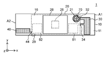
- FIG. 1A is a perspective view schematically showing an example of the appearance of a wireless module according to Embodiment 1.
- FIG. 1B is a top view schematically showing an example of the appearance of the wireless module in the first exemplary embodiment.
- FIG. 1C is a side view schematically showing an example of the appearance of the wireless module in the first exemplary embodiment.
- FIG. 1D is a bottom view schematically showing an example of the appearance of the wireless module in the first exemplary embodiment.
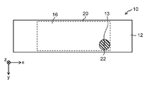
- FIG. 2 is a bottom view schematically showing an example of the appearance of the wireless module substrate according to the first embodiment.
- FIG. 3A is a top view schematically showing an example of the appearance of the wireless module in the second exemplary embodiment.
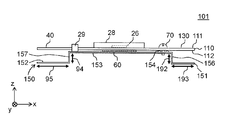
- FIG. 3B is a side view schematically showing an example of the appearance of the wireless module according to Embodiment 2.
- FIG. 3C is a bottom view schematically showing an example of the appearance of the wireless module in the second exemplary embodiment.
- FIG. 4 is a bottom view schematically showing an example of the appearance of the wireless module substrate according to the second embodiment.
- FIG. 5A is a top view schematically showing an example of the appearance of a wireless module according to Modification 1 of Embodiment 2.
- FIG. 5B is a side view schematically showing an example of the appearance of the wireless module in Modification 1 of Embodiment 2.
- FIG. 5C is a bottom view schematically showing an example of the appearance of the wireless module according to Modification 1 of Embodiment 2.
- FIG. 5A is a top view schematically showing an example of the appearance of a wireless module according to Modification 1 of Embodiment 2.
- FIG. 5B is a side view schematically showing an example of the appearance of the wireless module in Modification 1 of Embod
- FIG. 6 is a bottom view schematically showing an example of the appearance of the wireless module substrate in the first modification of the second embodiment.
- FIG. 7A is a top view schematically showing an example of the appearance of a wireless module in Modification 2 of Embodiment 2.
- FIG. 7B is a side view schematically showing an example of the appearance of the wireless module in the second modification of the second exemplary embodiment.
- FIG. 7C is a bottom view schematically showing an example of the appearance of the wireless module in the second modification of the second exemplary embodiment.
- FIG. 8 is a bottom view schematically showing an example of the appearance of the wireless module substrate according to the second modification of the second embodiment.
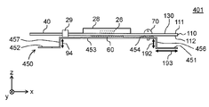
- FIG. 9A is a top view schematically showing an example of the appearance of the wireless module according to Embodiment 3.
- FIG. FIG. FIG. 9A is a top view schematically showing an example of the appearance of the wireless module according to Embodiment 3.
- FIG. FIG. FIG. 9A is a top view schematically showing an example of the appearance of the
- FIG. 9B is a side view schematically showing an example of the appearance of the wireless module according to Embodiment 3.
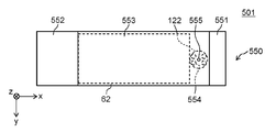
- FIG. 10 is a bottom view schematically showing an example of the appearance of the base plate of the wireless module in the third embodiment.
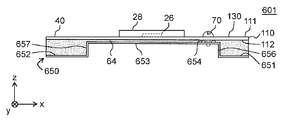
- FIG. 11A is a top view schematically showing an example of an appearance of a wireless module in the fourth exemplary embodiment.
- FIG. 11B is a side view schematically showing an example of the appearance of the wireless module in the fourth exemplary embodiment.
- FIG. 11C is a bottom view schematically showing an example of the appearance of the wireless module according to Embodiment 4.
- FIG. 12A is a top view schematically showing an example of an external appearance of a wireless module according to Modification 1 of Embodiment 4.
- FIG. 12B is a side view schematically showing an example of the appearance of the wireless module according to Modification 1 of Embodiment 4.
- FIG. 13A is a top view schematically showing an example of an external appearance of a wireless module according to Modification 2 of Embodiment 4.
- FIG. 13B is a side view schematically showing an example of the appearance of the wireless module in Modification 2 of Embodiment 4.
- FIG. 14 is a bottom view schematically showing an example of the appearance of the base plate of the wireless module in the second modification of the fourth embodiment.
- FIG. 15A is a top view schematically showing an example of an appearance of a wireless module in the fifth exemplary embodiment.
- FIG. 15B is a side view schematically showing an example of the appearance of the wireless module in the fifth exemplary embodiment.
- FIG. 15A is a top view schematically showing an example of an appearance of a wireless module in the fifth exemplary embodiment.
- FIG. 15B is a side view schematically showing an example of the appearance of the wireless module in the fifth
- FIG. 16 is a current intensity distribution diagram showing an example of the result of numerical analysis of a model corresponding to the wireless module in the fifth embodiment.
- FIG. 17A is a top view schematically showing an example of an external appearance of a wireless module according to Modification 1 of Embodiment 5.
- FIG. 17B is a side view schematically showing an example of the external appearance of the wireless module in Modification 1 of Embodiment 5.
- FIG. 18A is a top view schematically showing an example of an appearance of a wireless module in the sixth exemplary embodiment.
- FIG. 18B is a side view schematically showing an example of the appearance of the wireless module according to Embodiment 6.
- FIG. 19 is a bottom view schematically showing an example of the appearance of the base plate of the wireless module in the sixth embodiment.
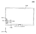
- FIG. 20 is a rear view schematically illustrating an example of an appearance of an image display device including the wireless module according to the seventh embodiment.
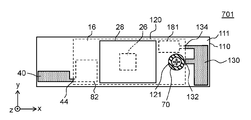
- FIG. 21 is an enlarged top view showing a portion where the wireless module is attached in the image display apparatus according to the seventh embodiment.
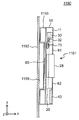
- FIG. 22 is an enlarged side view showing a portion where the wireless module is attached in the image display apparatus according to the seventh embodiment.
- Embodiment 1 the wireless module according to Embodiment 1 will be described with reference to FIGS. 1A to 2.
- FIG. 1A is a perspective view schematically showing an example of the appearance of the wireless module 1 according to the first embodiment.
- FIG. 1B is a top view schematically showing an example of the appearance of the wireless module 1 in the first embodiment.
- FIG. 1C is a side view schematically showing an example of the appearance of the wireless module 1 in the first exemplary embodiment.
- FIG. 1D is a bottom view schematically showing an example of the appearance of the wireless module 1 according to the first embodiment.
- FIG. 2 is a bottom view schematically showing an example of the appearance of the substrate 10 of the wireless module 1 according to the first embodiment.
- each figure used for the following explanation shows three axes of x-axis, y-axis, and z-axis
- the longitudinal axis of the wireless module 1 is the x-axis, is perpendicular to the x-axis direction, and is a wireless module.
- An axis in a direction perpendicular to the main surface of one substrate 10 is defined as a z-axis
- an axis orthogonal to both the x-axis and the z-axis is defined as a y-axis.
- the x-axis, y-axis, and z-axis are similarly defined. However, these axes are shown for convenience only and do not limit the present disclosure.
- the wireless module 1 is a wireless terminal that transmits and receives electromagnetic wave signals.
- the wireless module 1 is a wireless terminal based on a standard such as a wireless LAN (Local Area Network) or Bluetooth (registered trademark).
- the wireless module 1 includes a substrate 10, a ground pattern 20, a first antenna 30, a second antenna 40, and a ground plane 50.
- the wireless module 1 further includes a shield case 28, a first matching circuit 81, a second matching circuit 82, a conductive screw 70, and a spacer 29.
- the wireless module 1 further includes an IC (Integrated Circuit) 26 and a heat conducting member 60.
- the wireless module 1 according to the present embodiment may be a wireless module such as a MIMO (Multi-Input Multi-Output) method, a diversity method, or the like.
- the substrate 10 is a circuit board on which the ground pattern 20, the first antenna 30, and the second antenna 40 are formed and the IC 26 is mounted.
- the substrate 10 is a rectangular plate-like dielectric.
- the substrate 10 is, for example, a glass epoxy substrate.
- the substrate 10 includes a first main surface 11 on which the first antenna 30 and the second antenna 40 are formed, and a second main surface 12 facing away from the first main surface 11. .
- the ground pattern 20 is a wiring pattern arranged on the substrate 10 as shown in FIGS. 1A to 1C.
- the ground pattern 20 is formed on the first main surface 11 side and the second main surface 12 side of the substrate 10, and each ground pattern 20 is electrically connected to each other through a sufficient number of via electrodes (not shown).
- the ground pattern 20 is formed of, for example, a metal foil such as a copper foil, and is covered with the resist 16.
- the resist 16 is an insulating film that protects the wiring pattern formed on the substrate 10.
- the ground pattern 20 includes an exposed portion 21 provided on the first main surface 11 side of the substrate 10.
- the ground pattern 20 further includes an exposed portion 22 provided on the second main surface 12 side of the substrate 10.
- the exposed portion 21 and the exposed portion 22 are portions of the ground pattern 20 that are not covered with the resist 16 and are exposed to the outside. That is, in the present embodiment, the ground pattern 20 provided on the first main surface 11 side is covered with the resist 16 except for the exposed portion 21, and the ground pattern 20 provided on the second main surface 12 side is The resist 16 is covered except for the exposed portion 22.
- the exposed portion 21 and the exposed portion 22 are arranged at positions facing each other.
- the ground plane 50 is short-circuited with the ground pattern 20 via the exposed portion 21 and the exposed portion 22.
- the ground pattern 20 shows the structural example provided with the exposed part 21 and the exposed part 22, this indication is not limited to this structural example.
- the ground pattern 20 may include at least one of the exposed portion 21 and the exposed portion 22.
- the ground pattern 20 includes both the exposed portion 21 and the exposed portion 22, and the exposed portion 21 and the exposed portion 22 are connected to each other by the through-hole process in the through hole 13 of the substrate 10. With the configuration in which the via electrode is short-circuited, the uniformity of the potential of the ground pattern 20 can be improved.
- a through hole 13 is formed at the center of the exposed portion 22 of the ground pattern 20.
- a conductive screw 70 as an example of a fastening member is inserted into the through hole 13 from the first main surface 11 side of the substrate 10.
- the conductive screw 70 is an example of a conductive fastening member having a threaded portion.
- the ground plane 50 is fixed to the substrate 10 by the conductive screws 70 inserted into the through holes 13. Furthermore, the exposed portion 21 of the ground pattern 20 and the ground plane 50 are short-circuited via the conductive screw 70.
- the IC 26 is a circuit component that is mounted on the substrate 10 and connected to the ground pattern 20.
- the IC 26 is a component including a power amplifier and the like, for example, a wireless LAN chip.
- a high frequency signal amplified by a power amplifier included in the IC 26 is supplied to the first antenna 30 and the second antenna 40.
- the IC 26 is covered with a shield case 28.
- the shield case 28 is a metal box-like conductive member that covers the IC 26 mounted on the first main surface 11 of the substrate 10.
- the shield case 28 suppresses entry of electromagnetic noise from the outside to the inside of the shield case 28, and suppresses leakage of electromagnetic noise generated inside the shield case 28 to the outside.
- the shield case 28 is connected to the ground pattern 20 by soldering or the like. Thereby, the electromagnetic noise shielding effect by the shield case 28 is improved.
- the shield case 28 may cover not only the IC 26 but also other circuit elements.
- the first antenna 30 is disposed between one end A1 of the substrate 10 and the ground pattern 20, and is connected to the ground pattern 20. It is an antenna element provided with the 1st electric power feeding part 34 to which a signal is supplied.
- the first antenna 30 is formed between one end A ⁇ b> 1 in the x-axis direction of the substrate 10 (that is, the longitudinal direction of the substrate 10) and the ground pattern 20.
- the first antenna 30 is formed of a metal foil such as a copper foil, for example.
- the first antenna 30 is a PIFA (Planar Inverted-F Antenna) and functions as an antenna in combination with the ground plane 50.
- the resonance frequency of the first antenna 30 is not particularly limited, but is, for example, about 2.4 GHz.
- the pattern shape of the first antenna 30 is not limited to the shape shown in the drawing.
- the first antenna 30 may be, for example, a multiband antenna that supports multiband.
- the 1st antenna 30 shows the structural example arrange
- the 1st antenna 30 is arrange
- the first ground portion 32 of the first antenna 30 is a ground point connected to the ground pattern 20.
- the ground pattern 20 on the first main surface 11 side and the ground pattern 20 on the second main surface 12 side are electrically connected as close as possible to the first ground portion 32 via via electrodes or the like.
- the distance from the first ground portion 32 to the via electrode is set to about 1/20 or less of the wavelength of the electromagnetic wave used in the wireless module 1 (first antenna 30).
- the first antenna 30 may be formed integrally with the ground pattern 20 or may be connected to the ground pattern 20 by solder or the like.
- the first feeding unit 34 of the first antenna 30 is a part including a feeding point to which a first signal is supplied from the IC 26.
- the high frequency signal output from the IC 26 is supplied to the first power feeding unit 34 via the first matching circuit 81.
- the first antenna 30 may be formed integrally with the wiring pattern constituting the first matching circuit 81, or may be connected to the wiring pattern by solder or the like.
- the second antenna 40 is disposed between the other end A2 of the substrate 10 and the ground pattern 20, and includes an antenna element including a second feeding portion 44 to which a second signal is supplied. It is.
- the second antenna 40 is formed between the other end A ⁇ b> 2 in the x-axis direction of the substrate 10 (that is, the longitudinal direction of the substrate 10) and the ground pattern 20.
- the second antenna 40 is formed of a metal foil such as a copper foil, for example.
- the second antenna 40 is a monopole antenna.
- the pattern shape of the second antenna 40 is not limited to the shape shown in the drawing.
- the second antenna 40 may be, for example, a PIFA or a multiband antenna that supports multiband.
- the resonant frequency of the 2nd antenna 40 is not specifically limited, For example, it is about 2.4 GHz.
- the 2nd antenna 40 shows the structural example arrange
- the 2nd antenna 40 is arrange
- the second power feeding unit 44 of the second antenna 40 is a part including a power feeding point to which the first signal is supplied from the IC 26.
- the high frequency signal output from the IC 26 is supplied to the second power feeding unit 44 via the second matching circuit 82.
- the second antenna 40 may be formed integrally with a wiring pattern constituting the second matching circuit 82, or may be connected to the wiring pattern by solder or the like.
- the first matching circuit 81 is an impedance matching circuit for suppressing reflection of the high-frequency signal output from the IC 26 at the first antenna 30.
- the high frequency signal output from the IC 26 is input to the first matching circuit 81.
- the first matching circuit 81 outputs the high-frequency signal to the first power feeding unit 34 of the first antenna 30.
- the first matching circuit 81 is disposed between the IC 26 and the first antenna 30 on the first main surface 11 side of the substrate 10.
- the second matching circuit 82 is an impedance matching circuit for suppressing reflection of the high-frequency signal output from the IC 26 at the second antenna 40.
- the high frequency signal output from the IC 26 is input to the second matching circuit 82.
- the second matching circuit 82 outputs the high-frequency signal to the second power feeding unit 44 of the second antenna 40.
- the second matching circuit 82 is disposed between the IC 26 and the second antenna 40 on the first main surface 11 side of the substrate 10.
- the ground plane 50 includes a first facing portion 51 that faces the first antenna 30, a second facing portion 52 that faces the second antenna 40, and a third facing portion that faces the ground pattern 20 and is short-circuited to the ground pattern 20. 53, a conductive plate member.
- the ground plane 50 further includes a first gap forming part 56 and a second gap forming part 57.
- the ground plane 50 has a short-circuit point that short-circuits the ground plane 50 and the ground pattern 20 at the third facing portion 53. This short-circuit point is arranged at a position closer to the first facing portion 51 than the second facing portion 52 in the third facing portion 53. This short-circuit point will be described later.
- the ground plane 50 functions as an antenna together with the first antenna 30.
- the ground plane 50 has a configuration for improving the isolation between the first antenna 30 and the second antenna 40. This configuration will be described later.
- the ground plane 50 may function as a heat radiating member that dissipates heat generated by the IC 26.
- the ground plane 50 has a shape bent into a convex shape as shown in FIGS. 1A and 1C.
- the ground plane 50 is formed of, for example, a metal material such as aluminum, iron, or an alloy of various metals.
- the first facing portion 51 of the ground plane 50 is a portion disposed facing the first antenna 30.
- “the first facing portion 51 faces the first antenna 30” is not limited to the configuration in which the first facing portion 51 and the first antenna 30 face each other directly without using the substrate 10 or the like. This includes a configuration in which the first facing portion 51 and the first antenna 30 face each other with a non-conductive member such as the substrate 10 in between as in the present embodiment.
- the configuration in which the first antenna 30 is disposed on the first main surface 11 side of the substrate 10 or the configuration in which the first antenna 30 is disposed on the second main surface 12 side is the first of the ground plane 50.
- the facing portion 51 is included in the configuration arranged to face the first antenna 30.
- the first facing portion 51 has a substantially flat plate shape and is spaced apart from the first antenna 30 and the substrate 10. That is, a gap is formed between the first facing portion 51 and the first antenna 30.
- the distance between the 1st opposing part 51 and the 1st antenna 30 is 1/30 or more and about 1/10 or less of the wavelength of the electromagnetic waves used with the radio
- the first gap forming portion 56 of the ground plate 50 is a plate-like portion that is disposed between the first facing portion 51 and the third facing portion 53 and connects the first facing portion 51 and the third facing portion 53.
- the first gap forming portion 56 is disposed in a plane intersecting the substrate 10, thereby forming a gap between the first facing portion 51 and the first antenna 30.
- the first gap forming portion 56 is disposed in a plane substantially orthogonal to the substrate 10.
- the third facing portion 53 of the ground plane 50 is a plate-like portion that faces the ground pattern 20 and is short-circuited to the ground pattern.
- the ground plane 50 further includes one or a plurality of (for example, four) protrusions 54 on the third facing portion 53.
- the protruding portion 54 is disposed at a position facing the exposed portion 22 of the ground pattern 20 and is provided so as to be in contact with the exposed portion 22. Thereby, the ground plane 50 is short-circuited with the ground pattern 20.
- the base plate 50 is provided with a screw hole 55 at a position corresponding to the through hole 13, and a threaded portion of the conductive screw 70 penetrating the through hole 13 from the first main surface 11 side. Is screwed into the screw hole 55.
- the ground plane 50 is fixed to the substrate 10 and short-circuited to the exposed portion 21 of the ground pattern 20 via the conductive screw 70. That is, in the wireless module 1 according to the present embodiment, the projecting portion 54 and the screw hole 55 of the ground plane 50 constitute a short circuit point that short-circuits the ground plane 50 and the ground pattern 20.
- the ground plate 50 can be easily attached to the substrate 10 by having the above-described configuration, and the ground plate 50 is short-circuited to the ground pattern 20 with high accuracy. Can do. Moreover, in the structure shown in this Embodiment, since the ground plane 50 is attached to the board
- the wireless module 1 is provided with a total of five short-circuit points including the four protrusions 54 and the screw holes 55.
- the number of short-circuit points provided in the wireless module 1 is equal to this number. It is not limited to. For example, the number of short-circuit points may be one. As described above, in the wireless module 1 shown in the present embodiment, it is not necessary to provide two short-circuit members as in the wireless communication device disclosed in Patent Document 1.
- the position where the ground plane 50 and the ground pattern 20 are short-circuited that is, the arrangement position of the exposed portion 21 and the exposed portion 22 greatly affects the radiation characteristics of the antenna unit constituted by the first antenna 30 and the ground plane 50.
- the short-circuit point between the ground plane 50 and the ground pattern 20 is arranged as close as possible to the first grounding portion 32, good and stable radiation characteristics as an antenna unit can be obtained.
- the configuration in which the exposed portion 21 is directly connected to the first ground portion 32 or the distance from the short-circuit point between the ground plane 50 and the ground pattern 20 to the first ground portion 32 is the wavelength of the electromagnetic wave used in the wireless module 1.
- the wireless module 1 can obtain stable radiation characteristics.
- the portions of the third facing portion 53 other than the protrusions 54 are arranged away from the ground pattern 20 by a predetermined distance.
- the predetermined distance is, for example, 1/500 or more and 1/50 or less of the resonance wavelength of the first antenna 30. In the present embodiment, the predetermined distance is about 0.5 mm.
- the second facing portion 52 of the ground plane 50 is a portion disposed facing the second antenna 40.
- the second facing portion 52 has a substantially flat plate shape and is disposed apart from the second antenna 40 and the substrate 10. That is, a gap is formed between the second facing portion 52 and the second antenna 40.
- the distance between the second facing portion 52 and the second antenna 40 is, for example, about 1/30 to 1/10 of the wavelength of the electromagnetic wave used in the wireless module 1 (second antenna 40).
- the second gap forming portion 57 of the ground plate 50 is a plate-like portion that is disposed between the second facing portion 52 and the third facing portion 53 and connects the second facing portion 52 and the third facing portion 53.
- the second gap forming part 57 is disposed in a plane intersecting the substrate 10, thereby forming a gap between the second facing part 52 and the second antenna 40.
- the second gap forming portion 57 is disposed in a plane substantially orthogonal to the substrate 10.
- the spacer 29 is a member for stably maintaining the distance between the substrate 10 and the third facing portion 53 of the ground plane 50.
- the spacer 29 has a plate shape bent into a substantially U shape, and a part thereof is inserted between the substrate 10 and the third facing portion 53.
- the thickness of the portion of the spacer 29 that is inserted between the substrate 10 and the third facing portion 53 is approximately the same as the distance between the substrate 10 and the third facing portion 53. Thereby, the space
- the spacer 29 is formed of an insulating material.
- the spacer 29 is made of, for example, an insulating resin.
- the heat conducting member 60 is a member that is disposed between the ground plane 50 and the IC 26 and conducts heat generated by the IC 26 to the ground plane 50.
- the heat conducting member 60 is disposed at a position facing the IC 26 between the second main surface 12 of the substrate 10 and the ground plane 50. Further, the heat conducting member 60 is disposed so as to contact the second main surface 12 and the ground plane 50.
- the heat conductive member 60 includes, for example, a heat conductive elastomer as a material used.
- the heat conducting member 60 is formed of heat radiating rubber containing silicone or the like as a material used. Thereby, since the heat conductive member 60 has elasticity, the adhesiveness with the board
- the ground plane 50 includes a configuration that improves the isolation between the first antenna 30 and the second antenna 40 as described above. That is, a configuration is provided that can reduce the interference of the electromagnetic wave output from one antenna with the other antenna.
- the ground plane 50 has a short circuit point at the third facing portion 53 to short-circuit the ground plane 50 and the ground pattern 20.
- This short-circuit point is arranged at a position closer to the first facing portion 51 than the second facing portion 52 in the third facing portion 53.
- part of the current flowing from the first ground portion 32 of the first antenna 30 to the ground pattern 20 flows to the ground plane 50.
- the current flowing from the first antenna 30 to the ground pattern 20 is reduced, whereby the current flowing to the vicinity of the second antenna 40 of the ground pattern 20 is reduced.
- the wireless module 1 it is possible to suppress the influence of the current flowing from the first antenna 30 to the ground pattern 20 on the second antenna 40. That is, in the wireless module 1, it is possible to improve the isolation between the first antenna 30 and the second antenna 40.
- the electrical length from the short-circuit point that short-circuits the ground plane 50 and the ground pattern 20 to the vertex 51t that is closest to the short-circuit point of the ground plane 50 is set to a predetermined length.
- the isolation between the first antenna 30 and the second antenna 40 can be improved.
- the ground plane 50 has four vertices at positions where each end edge at both ends in the x-axis direction and each end edge at both ends in the y-axis direction intersect.
- the vertex of the ground plane 50 closest to the short-circuit point is the vertex at the position where the edge of the end B1 in the x-axis direction of the ground plane 50 and the edge of the end C1 in the y-axis direction intersect. 51t (see FIGS. 1A and 1D).
- the electrical length from the short-circuit point that short-circuits the ground plane 50 and the ground pattern 20 to the vertex 51t corresponds to the leg of the perpendicular line from the short-circuit point to the edge of the ground plane 50 closest to the short-circuit point. It is defined as the sum of the distance to the point (the distance indicated by the arrow 91 in FIGS. 1A and 1D) and the length of the edge of the ground plane 50 from the point to the vertex 51t.
- the electrical length from the short circuit point which short-circuits the ground plane 50 and the ground pattern 20 to the vertex 51t nearest to the said short circuit point of the ground plane 50 is shown typically, the length will be shown to FIG. 1A.
- the four protrusions 54 and the screw holes 55 of the main plate 50 correspond to short-circuit points.
- the electrical length from the short-circuit point to the vertex 51t is defined as the shortest electrical length among the electrical lengths from the vertex 51t to each short-circuit point.
- the inventors of the present application improve the isolation between the two antennas (between the first antenna 30 and the second antenna 40) by setting the electrical length to approximately 1 ⁇ 4 of the resonance wavelength of the first antenna 30. I found out that I can do it.
- about 1/4 of the resonance wavelength specifically means that it is about 1/8 or more and 3/8 or less of the resonance wavelength.
- the cause of the correlation between the electrical length and the isolation between the two antennas is estimated as follows.
- an antenna current is generated in the first antenna 30 and the ground pattern 20.
- the electrical length from the short-circuit point that short-circuits the ground plane 50 and the ground pattern 20 to the vertex 51t is approximately 1 ⁇ 4 of the resonance wavelength, the vertex 51t becomes a node of current, and the short-circuit point becomes an antinode of current.
- Standing waves Thereby, the antenna current flowing through the ground pattern 20 is distributed to the path toward the second antenna 40 and the path toward the first facing portion 51, and the current input to the second antenna 40 decreases.
- the wireless module 1 can improve the isolation between the two antennas. Guessed.
- the isolation between the two antennas in the wireless module 1 can be improved by optimizing the size of the portion of the ground plane 50 near the second antenna 40. Specifically, the inventors set the electrical length from the end of the base plate 50 on the second facing portion 52 side of the third facing portion 53 to the end of the second facing portion 52 opposite to the third facing portion 53. It has been found that the isolation between the two antennas can be improved in the wireless module 1 by setting the frequency to about 1 ⁇ 4 of the resonance wavelength of the first antenna 30. Here, approximately 1/4 of the resonance wavelength specifically means that it is about 1/8 or more and 3/8 or less of the resonance wavelength.
- the length is equal to the length of the edge of the second gap forming portion 57 indicated by the arrow 94 in FIGS. 1A and 1C, and FIGS. 1A and 1C. It is shown as the sum of the length from the edge on the third facing portion 53 side of the second facing portion 52 to the edge on the opposite side of the third facing portion 53 indicated by the arrow 95.
- the size of the ground plane 50 in the width direction (y-axis direction) of the ground plane 50 is not limited near the second antenna 40. This is because, in the vicinity of the second antenna 40, the direction of the current flowing from the short-circuit point that short-circuits the ground plane 50 and the ground pattern 20 to the ground plane 50 is substantially parallel to the longitudinal direction (x-axis direction) of the ground plane 50. This is because the influence of the size in the width direction of the ground plane 50 on the current is reduced.
- the isolation between the first antenna 30 and the second antenna 40 can be improved by optimizing the size of the ground plane 50. Furthermore, the isolation characteristic is less sensitive to changes in the resonance wavelength than, for example, the isolation characteristic in the technique using the slit disclosed in Patent Document 1. That is, in the wireless module 1 according to the present embodiment, it is possible to ensure isolation between the first antenna 30 and the second antenna 40 in a relatively wide frequency band.
- the first antenna 30 and the second antenna 40 can be used in frequency bands close to each other.
- the first antenna 30 can be used as a Bluetooth (registered trademark) antenna of about 2.4 GHz band
- the second antenna 40 can be used as an antenna for a wireless LAN of about 2.4 GHz band.
- the wireless module includes the substrate, the ground pattern disposed on the substrate, the first antenna, the second antenna, and the conductive ground plane.
- the first antenna is disposed between one end of the substrate and the ground pattern, and includes a grounding unit connected to the ground pattern and a first power feeding unit to which a first signal is supplied.
- the second antenna is disposed between the other end of the substrate and the ground pattern, and has a second power feeding unit to which a second signal is supplied.
- the ground plane includes a first facing portion that faces the first antenna, a second facing portion that faces the second antenna, and a third facing portion that faces the ground pattern and is short-circuited to the ground pattern.
- a ground plane has a short circuit point which short-circuits a ground plane and a ground pattern in a 3rd opposing part.
- the short-circuit point is arranged at a position closer to the first facing portion than the second facing portion in the third facing portion.
- the wireless module 1 is an example of a wireless module.
- the substrate 10 is an example of a substrate.
- the ground pattern 20 is an example of a ground pattern.
- the first antenna 30 is an example of a first antenna.
- the second antenna 40 is an example of a second antenna.
- the ground plane 50 is an example of a ground plane.
- One end A1 is an example of one end of the substrate.
- the first grounding part 32 is an example of a grounding part.
- the first power supply unit 34 is an example of a first power supply unit.
- the other end A2 is an example of the other end of the substrate.
- the second power supply unit 44 is an example of a second power supply unit.
- the first facing portion 51 is an example of a first facing portion.
- the second facing portion 52 is an example of a second facing portion.
- the third facing portion 53 is an example of a third facing portion.
- the wireless module 1 includes a substrate 10 and a ground pattern 20 disposed on the substrate 10.
- the wireless module 1 is further disposed between the one end A1 of the substrate 10 and the ground pattern 20, and is connected to the ground pattern 20, and a first power feeding unit 34 to which a first signal is supplied.
- a first antenna 30 is provided.
- the wireless module 1 further includes a second antenna 40 that is disposed between the other end A2 of the substrate 10 and the ground pattern 20 and has a second power feeding unit 44 to which a second signal is supplied. Further, the wireless module 1 is further short-circuited to the ground pattern 20, facing the first pattern 51 facing the first antenna 30, facing the second pattern 52 facing the second antenna 40, and the ground pattern 20.
- a conductive ground plane 50 having a third opposing portion 53 is provided.
- the ground plane 50 has a short circuit point that short-circuits the ground plane 50 and the ground pattern 20 to the third facing portion 53.
- the short-circuit point is arranged at a position in the third facing portion 53 that is closer to the first facing portion 51 than the second facing portion 52.
- the wireless module 1 configured as described above, a part of the current flowing from the first ground portion 32 of the first antenna 30 to the ground pattern 20 flows to the ground plane 50. As described above, by reducing the current flowing from the first antenna 30 to the ground pattern 20, in the wireless module 1, the current flowing to the vicinity of the second antenna 40 of the ground pattern 20 is reduced. For this reason, in the wireless module 1, the isolation between the first antenna 30 and the second antenna 40 can be improved.
- the short circuit point may be arranged in the vicinity of the grounding unit.
- the short-circuit point is arranged in the vicinity of the first grounding unit 32.
- the wireless module 1 good radiation characteristics can be obtained in the antenna unit constituted by the first antenna 30 and the ground plane 50.
- the electrical length from the short-circuit point to the apex closest to the short-circuit point of the ground plane may be approximately 1 ⁇ 4 of the resonance wavelength of the first antenna.
- vertex 51t is an example of the vertex closest to the short-circuit point of the ground plane.
- the electrical length from the short-circuit point that short-circuits the ground plane 50 and the ground pattern 20 to the vertex 51t that is closest to the short-circuit point of the ground plane 50 is the first This is approximately 1 ⁇ 4 of the resonance wavelength of the antenna 30.
- the isolation between the first antenna 30 and the second antenna 40 can be improved.
- the electrical length from the end of the third facing portion on the second facing portion side to the end of the second facing portion opposite to the third facing portion is approximately 1 ⁇ 4 of the resonance wavelength of the first antenna. There may be.
- the third opposing portion 53 of the second opposing portion 52 is opposite.
- the electrical length to the end on the side is approximately 1 ⁇ 4 of the resonance wavelength of the first antenna 30.
- the isolation between the first antenna 30 and the second antenna 40 can be improved.
- the wireless module may further include a conductive fastening member that is disposed at the short-circuit point and fastens the substrate and the ground plane.
- the conductive screw 70 is an example of a conductive fastening member.
- the wireless module 1 further includes a conductive screw 70 that is disposed at the short-circuit point and fastens the substrate 10 and the ground plane 50.
- the ground plane 50 can be stably fixed to the substrate 10. Further, by using the conductive screw 70 as the fastening member, the base plate 50 can be easily attached to and detached from the substrate 10. Further, by bringing the conductive screw 70 into contact with the exposed portion 21 of the ground pattern 20, the wireless module 1 can short-circuit the ground pattern 20 and the ground plane 50 via the conductive screw 70.
- the first antenna may be a PIFA (Planar Inverted-F Antenna).
- the first antenna 30 is a PIFA.
- the first antenna 30 functions as an antenna when combined with the ground plane 50.
- the wireless module 101 according to the present embodiment has substantially the same configuration as the wireless module 1 described in the first embodiment.
- the wireless module 101 shown in the second embodiment is different from the wireless module 1 according to the first embodiment in the position of the short circuit point that short-circuits the ground plane and the ground pattern.
- the description of the matters described in Embodiment 1 will be omitted as appropriate, and differences from the wireless module 1 according to Embodiment 1 will be mainly described.
- symbol same as the component is provided, and the description is abbreviate
- FIG. 3A is a top view schematically showing an example of the appearance of the wireless module 101 in the second embodiment.
- FIG. 3B is a side view schematically showing an example of the appearance of the wireless module 101 in the second exemplary embodiment.
- FIG. 3C is a bottom view schematically showing an example of the appearance of the wireless module 101 in the second exemplary embodiment.
- FIG. 4 is a bottom view schematically showing an example of the appearance of the substrate 110 of the wireless module 101 in the second embodiment.
- the wireless module 101 includes a substrate 110, a ground pattern 120, an IC 26, a shield case 28, a first antenna 130, a second antenna 40, a first matching circuit 181, Two matching circuits 82 and a spacer 29 are provided. As illustrated in FIG. 3B, the wireless module 101 further includes a ground plane 150, a conductive screw 70, and a heat conducting member 60.
- the ground pattern 120 includes an exposed portion 121 provided on the first main surface 111 side of the substrate 110.
- the ground pattern 120 further includes an exposed portion 122 provided on the second main surface 112 side of the substrate 110.
- the exposed portion 121 and the exposed portion 122 are portions of the ground pattern 120 that are not covered with the resist 16 and are exposed to the outside.
- the exposed part 121 and the exposed part 122 are arranged at positions facing each other.
- exposed portion 121 and exposed portion 122 are formed in the center of substrate 110 in the width direction (y-axis direction).
- the substrate 110 includes a first main surface 111 on which the first antenna 130 and the second antenna 40 are formed, and a second main surface 112 facing away from the first main surface 111. .
- a through hole 113 is formed in the substrate 110 at the center of the exposed portion 121 and the exposed portion 122 of the ground pattern 120.
- Substrate 110 is mainly arranged such that first feeding unit 134 and first grounding unit 132 of first antenna 130 are arranged at first feeding unit 34 and first antenna 30 of first antenna 30 of substrate 10 according to the first embodiment. It is different from the arrangement position of the grounding portion 32.
- the first ground portion 132 of the first antenna 130 is disposed near the center in the width direction (y-axis direction) of the substrate 110 in accordance with the positions of the exposed portions 121 and 122 in the ground pattern 120. ing.
- the first power feeding unit 134 of the first antenna 130 is disposed in the vicinity of the end of the substrate 110 in the width direction so as not to interfere with the first grounding unit 132.
- the first matching circuit 181 is substantially the same circuit as the first matching circuit 81 according to the first embodiment. However, in the substrate 110, the layout of the first matching circuit 181 is different from the layout of the first matching circuit 81 in the substrate 10 of the first embodiment. In the substrate 110, the first matching circuit 181 is arranged at a position that does not interfere with the arrangement position of the exposed portion 121 of the ground pattern 120. In the first matching circuit 181, the position of the output unit is set in accordance with the arrangement position of the first power feeding unit 134 of the first antenna 130.
- the ground plane 150 includes a first facing portion 151, a second facing portion 152, a third facing portion 153, a first gap forming portion 156, and a second gap forming. Part 157 (see FIG. 3B).
- the ground plane 150 has a short-circuit point that short-circuits the ground plane 150 and the ground pattern 120 at the third facing portion 153. This short-circuit point is arranged at a position closer to the first facing portion 151 than the second facing portion 152 in the third facing portion 153.
- the ground plate 150 has one or a plurality of (for example, four) protrusions 154 on the third facing portion 153.
- the protruding portion 154 is disposed at a position facing the exposed portion 122 of the ground pattern 120 and is provided so as to be in contact with the exposed portion 122.
- the base plate 150 is provided with a screw hole 155 at a position corresponding to the through hole 113, and the screw portion of the conductive screw 70 that penetrates the through hole 113 from the first main surface 111 side of the substrate 110 is a screw hole. 155.
- the ground plane 150 is fixed to the substrate 110 and short-circuited to the exposed portion 121 of the ground pattern 120 via the conductive screw 70.
- the exposed portion 122 and the protruding portion 154 are short-circuited.
- the projecting portion 154 and the screw hole 155 of the ground plane 150 constitute a short-circuit point that short-circuits the ground plane 150 and the ground pattern 120.
- the protrusions 154 and the screw holes 155 are arranged on the first facing portion 151 side of the third facing portion 153 in accordance with the arrangement positions of the exposed portions 121 and the exposed portions 122 of the ground pattern 120.
- positioned in the approximate center of an edge direction differs from the ground plane 50 which concerns on Embodiment 1.
- the edge direction means the width direction (y-axis direction) of the ground plane 150, and the approximate center in the edge direction is a range of about 10% of the width from the center in the width direction of the ground plane 150. Means.
- the length of the first facing portion 151 in the x-axis direction is different from the length of the first facing portion 51 according to the first embodiment in the x-axis direction.
- the length of the first facing portion 151 in the x-axis direction will be described later.
- the ground plane 150 has a short-circuit point that short-circuits the ground plane 150 and the ground pattern 120 at the third facing portion 153, similarly to the ground plane 50 of the first embodiment.
- This short-circuit point is arranged at a position closer to the first facing portion 151 than the second facing portion 152 in the third facing portion 153.
- the electrical length up to is determined.
- the electrical length is schematically shown as the sum of the lengths of the arrows 191, 192, and 193 shown in FIGS. 3A to 3C.
- the electrical length is about 1 ⁇ 4 of the resonance wavelength of the first antenna 130.
- the electrical length from the end of the third facing portion 153 on the second facing portion 152 side to the end of the second facing portion 152 on the side opposite to the third facing portion 153 is the wireless length of the first embodiment.
- the length of the electrical length is schematically shown as the sum of the distance indicated by the arrow 94 and the distance indicated by the arrow 95 in FIGS. 3B and 3C.
- the wireless module 101 can further improve the isolation between both antennas (between the first antenna 130 and the second antenna 40).
- the short-circuit point that short-circuits the ground plane 150 and the ground pattern 120 is disposed at the approximate center in the width direction (y-axis direction) of the ground plane 150. Therefore, the distance from the short-circuit point to the point corresponding to the leg of the perpendicular from the short-circuit point to the edge of the ground plane 150 closest to the short-circuit point (distance indicated by the arrow 191 in FIGS. 3A and 3C) Is longer than the distance according to Embodiment 1 (the distance indicated by the arrow 91 in FIGS. 1A and 1D).
- the electrical length from the short-circuit point that short-circuits the ground plane 150 and the ground pattern 120 to the vertex 151t closest to the short-circuit point of the ground plane 150 is approximately 1 of the resonance wavelength of the first antenna 130. / 4 is set. Therefore, since the distance indicated by the arrow 191 is longer than the distance indicated by the arrow 91 in the first embodiment, the length of the edge of the ground plate 150 from the point corresponding to the perpendicular foot to the vertex 151t is The length is set shorter than the length of the first embodiment. For example, the length in the z-axis direction of the first gap forming portion 156 (the distance indicated by the arrow 192 in FIG.
- the length in the x-axis direction of the first facing portion 151 of the main plate 150 is shortened. Can do. Thereby, the wireless module 101 can be reduced in size. Along with this, the cost required for the main plate 150 can be reduced.
- the wireless module in this embodiment has substantially the same configuration as the wireless module shown in Embodiment 1, and can obtain substantially the same effect.
- the wireless module 101 is an example of a wireless module.
- the substrate 110 is an example of a substrate.
- the ground pattern 120 is an example of a ground pattern.
- the first antenna 130 is an example of a first antenna.
- the ground plane 150 is an example of a ground plane.
- the first ground portion 132 is an example of a ground portion.
- the first power supply unit 134 is an example of a first power supply unit.
- the first facing portion 151 is an example of a first facing portion.
- the second facing portion 152 is an example of a second facing portion.
- the third facing portion 153 is an example of a third facing portion.
- the short-circuit point may be arranged at the approximate center in the edge direction on the first facing portion side in the third facing portion.
- the short-circuit point that short-circuits the ground plane 150 and the ground pattern 120 is approximately the center in the edge direction on the first facing portion 151 side in the third facing portion 153. Is arranged.
- the approximate center may be defined as, for example, that the exposed portion 121 or the exposed portion 122 is disposed at a position including the center.
- the wireless module 101 from the short circuit point that short-circuits the ground plane 150 and the ground pattern 120 to the vertex 151t closest to the short circuit point of the ground plane 150, from the short circuit point to the edge of the ground plane 150.
- the wireless module 201 according to this modification has substantially the same configuration as the wireless module 1 described in the first embodiment.
- the wireless module 201 shown in this modification is different from the wireless module 1 according to the first embodiment in the configuration of a short-circuit point that short-circuits the ground plane and the ground pattern.
- the description of the matters described in the first embodiment will be omitted as appropriate, and differences from the wireless module 1 according to the first embodiment will be mainly described.
- symbol same as the component is provided, and the description is abbreviate
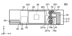
- FIG. 5A is a top view schematically showing an example of the appearance of the wireless module 201 in the first modification of the second embodiment.
- FIG. 5B is a side view schematically showing an example of the appearance of the wireless module 201 in the first modification of the second embodiment.
- FIG. 5C is a bottom view schematically showing an example of the appearance of the wireless module 201 in the first modification of the second embodiment.
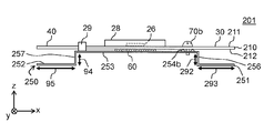
- FIG. 6 is a bottom view schematically showing an example of the appearance of the substrate 210 of the wireless module 201 in the first modification of the second embodiment.
- the wireless module 201 includes a substrate 210, a ground pattern 220, an IC 26, a shield case 28, a first antenna 30, a second antenna 40, a first matching circuit 281 and a first matching circuit 281.
- the second matching circuit 82, the spacer 29, the conductive screw 70, the conductive screw 70a, and the conductive screw 70b are provided.
- the wireless module 201 further includes a ground plane 250 and a heat conducting member 60.
- the ground pattern 220 includes an exposed portion 221, an exposed portion 221a, and an exposed portion 221b provided on the first main surface 211 side of the substrate 210.
- the ground pattern 220 further includes an exposed portion 222, an exposed portion 222a, and an exposed portion 222b provided on the second main surface 212 side of the substrate 210.
- the exposed portion 221, the exposed portion 221a, the exposed portion 221b, the exposed portion 222, the exposed portion 222a, and the exposed portion 222b are portions of the ground pattern 220 that are not covered with the resist 16 and are exposed to the outside.
- the exposed part 221 and the exposed part 222 are arranged at positions facing each other.
- the exposed part 221a and the exposed part 222a are disposed at positions facing each other.
- the exposed part 221b and the exposed part 222b are arranged at positions facing each other.
- the exposed portion 221, the exposed portion 221a, and the exposed portion 221b, and the exposed portion 222, the exposed portion 222a, and the exposed portion 222b are arranged in the width direction (y-axis direction) of the substrate 210.
- the substrate 210 includes a first main surface 211 on which the first antenna 30 and the second antenna 40 are formed, and a second main surface 212 facing away from the first main surface 211. .
- a through hole 213 is formed in the center of the exposed portion 221 and the exposed portion 222 of the ground pattern 220, and a through hole is formed in the center of the exposed portion 221a and the exposed portion 222a.
- a hole 213a is formed, and a through hole 213b is formed at the center of the exposed portion 221b and the exposed portion 222b.
- the first matching circuit 281 is substantially the same circuit as the first matching circuit 81 according to the first embodiment. However, in the substrate 210, the layout of the first matching circuit 281 is different from the layout of the first matching circuit 81 in the substrate 10 of the first embodiment. In the substrate 210, the first matching circuit 281 is arranged at a position that does not interfere with the arrangement position of each exposed portion of the ground pattern 220. In the first matching circuit 281, the position of the output unit is set in accordance with the arrangement position of the first power feeding unit 34 of the first antenna 30.
- the ground plane 250 is composed of a first facing portion 251, a second facing portion 252, a third facing portion 253, a first gap forming portion 256, and a second gap forming. Part 257 (see FIG. 5B).
- the ground plane 250 has a short-circuit point that short-circuits the ground plane 250 and the ground pattern 220 at the third facing portion 253. This short circuit point is arranged at a position in the third facing portion 253 that is closer to the first facing portion 251 than the second facing portion 252.
- the ground plate 250 has one or a plurality of (for example, four) protrusions 254 at positions corresponding to the exposed portions 222 of the ground pattern 220, and positions corresponding to the exposed portions 222a.
- the protruding portion 254 is in contact with the exposed portion 222
- the protruding portion 254a is in contact with the exposed portion 222a
- the protruding portion 254b is provided in contact with the exposed portion 222b.
- the base plate 250 is provided with a screw hole 255 at a position corresponding to the through hole 213, and is provided with a screw hole 255a at a position corresponding to the through hole 213a, corresponding to the through hole 213b.
- the screw hole 255b is provided in the position to do. Then, the screw portion of the conductive screw 70 penetrating the through hole 213 from the first main surface 211 side of the substrate 210 is screwed into the screw hole 255 and penetrates the through hole 213a from the first main surface 211 side of the substrate 210.
- the screw portion of the conductive screw 70a is screwed into the screw hole 255a, and the screw portion of the conductive screw 70b passing through the through hole 213b from the first main surface 211 side of the substrate 210 is screwed into the screw hole 255b. Accordingly, the ground plane 250 is fixed to the substrate 210 and short-circuited with the exposed portion 221, the exposed portion 221a, and the exposed portion 221b of the ground pattern 220 via the conductive screw 70, the conductive screw 70a, and the conductive screw 70b.
- the exposed portion 222 and the protruding portion 254 are short-circuited, the exposed portion 222a and the protruding portion 254a are short-circuited, and the exposed portion 222b and the protruding portion 254b are short-circuited.
- the projecting portion 254, the projecting portion 254a, the projecting portion 254b, the screw hole 255, the screw hole 255a, and the screw hole 255b of the ground plate 250 are connected to the ground plate 250 and the ground pattern 220. Configure a short-circuit point to short-circuit.
- the ground plane 250 and the ground pattern 220 are short-circuited at positions corresponding to the exposed portion 222, the exposed portion 222a, and the exposed portion 222b of the ground pattern 220.
- Short-circuit points are formed, and the short-circuit points are arranged in the width direction (y-axis direction) of the main plate 250.
- the number and position of the short-circuit points of the wireless module 201 may be adjusted as appropriate.
- the electrical length from the short circuit point which short-circuits the ground plane 250 and the ground pattern 220 to the edge nearest to the said short circuit point of the ground plane 250 can be set to desired length.
- the electrical length from the short-circuit point that short-circuits the ground plane 250 and the ground pattern 220 to the vertex closest to the short-circuit point of the ground plane 250 is the wireless module of the first embodiment. It is determined in the same way as 1. That is, when the electrical length is schematically shown, the length is defined as the sum of the length of the arrow 291 in FIG. 5C, the length of the arrow 292 in FIG. 5B, and the length of the arrow 293.
- the electrical length from the short-circuit point that short-circuits the ground plane 250 and the ground pattern 220 to the vertex closest to the short-circuit point of the ground plane 250 is the wireless module 1 of the first embodiment.
- the resonance wavelength of the first antenna 30 is approximately 1 ⁇ 4.
- the ground plane 250 by setting the electrical length from the short-circuit point that short-circuits the ground plane 250 and the ground pattern 220 to the edge closest to the short-circuit point of the ground plane 250 to a desired length, the ground plane 250
- the length of the first gap forming portion 256 in the z-axis direction (the distance indicated by the arrow 292 in FIG. 5B) and the length of the first facing portion 251 in the x-axis direction (in the arrow 293 in FIGS. 5B and 5C) The distance shown) can be adjusted to the desired length.
- the wireless module according to the present modification has substantially the same configuration as the wireless module described in Embodiment 1, and can obtain substantially the same effect.
- the wireless module 201 is an example of a wireless module.
- the substrate 210 is an example of a substrate.
- the ground pattern 220 is an example of a ground pattern.
- the ground plane 250 is an example of a ground plane.
- the first facing portion 251 is an example of a first facing portion.
- the second facing portion 252 is an example of a second facing portion.
- the third facing portion 253 is an example of a third facing portion.
- the position and number of the exposed portions of the ground pattern 220 and the position and number of the protrusions 254 of the ground plate 250 are adjusted, so that the ground plate 250 and the ground pattern are adjusted.
- the position and number of short-circuit points that short-circuit 220 are adjusted.
- the electrical length from the short-circuit point that short-circuits the ground plane 250 and the ground pattern 220 to the edge closest to the short-circuit point of the ground plane 250 is set to a desired length.
- the electrical length from the short-circuit point to the apex closest to the short-circuit point of the ground plane 250 is approximately 1 ⁇ 4 of the resonance wavelength of the first antenna 30, the first of the ground plane 250
- the dimensions of the one gap forming portion 256 and the first facing portion 251 can be adjusted to a desired size.
- the wireless module 301 according to this modification has substantially the same configuration as the wireless module 1 described in the first embodiment.
- the wireless module 301 shown in the present modification is different from the wireless module 1 according to the first embodiment in the configuration of a short-circuit point that short-circuits the ground plane and the ground pattern.
- the description of the matters described in the first embodiment will be omitted as appropriate, and differences from the wireless module 1 according to the first embodiment will be mainly described.
- symbol same as the component is provided, and the description is abbreviate
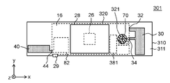
- FIG. 7A is a top view schematically showing an example of the appearance of the wireless module 301 in the second modification of the second embodiment.
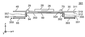
- FIG. 7B is a side view schematically showing an example of the appearance of the wireless module 301 in the second modification of the second embodiment.
- FIG. 7C is a bottom view schematically showing an example of the appearance of the wireless module 301 in the second modification of the second embodiment.
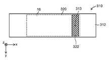
- FIG. 8 is a bottom view schematically showing an example of the appearance of the substrate 310 of the wireless module 301 in the second modification of the second embodiment.
- the wireless module 301 includes a substrate 310, a ground pattern 320, an IC 26, a shield case 28, a first antenna 30, a second antenna 40, a first matching circuit 381, and a first matching circuit 381. Two matching circuits 82 and a spacer 29 are provided. As shown in FIG. 7B, the wireless module 301 further includes a ground plane 350, a conductive screw 70, and a heat conducting member 60.
- the ground pattern 320 includes an exposed portion 321 provided on the first main surface 311 side of the substrate 310. Further, as shown in FIG. 8, the ground pattern 320 further includes an exposed portion 322 provided on the second main surface 312 side of the substrate 310.
- the exposed portion 321 and the exposed portion 322 are portions of the ground pattern 320 that are not covered with the resist 16 and are exposed to the outside.
- the exposed portion 322 has a rectangular shape extending in the width direction (y-axis direction) of the substrate 310. The exposed portion 322 is disposed at a position including a region facing the exposed portion 321.
- the substrate 310 includes a first main surface 311 on which the first antenna 30 and the second antenna 40 are formed, and a second main surface 312 facing away from the first main surface 311. . Further, as shown in FIG. 8, in the substrate 310, a through hole 313 is formed in the center of the exposed portion 322 of the ground pattern 320.
- the first matching circuit 381 is substantially the same circuit as the first matching circuit 81 according to the first embodiment. However, in the substrate 310, the layout of the first matching circuit 381 is different from the layout of the first matching circuit 81 in the substrate 10 of the first embodiment. In the substrate 310, the first matching circuit 381 is arranged at a position that does not interfere with the arrangement position of the exposed portion 321 of the ground pattern 320. In the first matching circuit 381, the position of the output unit is set in accordance with the arrangement position of the first power feeding unit 34 of the first antenna 30.
- the ground plane 350 includes a first facing portion 351, a second facing portion 352, a third facing portion 353, a first gap forming portion 356, and a second gap forming. Part 357 (see FIG. 7B).
- the ground plane 350 has a short circuit point that short-circuits the ground plane 350 and the ground pattern 320 at the third facing portion 353. This short-circuit point is arranged at a position closer to the first facing portion 351 than the second facing portion 352 in the third facing portion 353.
- the ground plate 350 has one or a plurality of protrusions 354 at positions corresponding to the exposed portions 322 of the ground pattern 320.
- the protrusion 354 is provided so as to be in contact with the exposed portion 322.
- the number of protrusions 354 is not particularly limited, but in the present modification, the number of protrusions 354 included in the ground plane 350 is twelve.
- the base plate 350 is provided with a screw hole 355 at a position corresponding to the through hole 313. Then, the screw portion of the conductive screw 70 penetrating the through hole 313 from the first main surface 311 side of the substrate 310 is screwed into the screw hole 355.
- the ground plane 350 is fixed to the substrate 310 and short-circuited to the exposed portion 321 of the ground pattern 320 via the conductive screw 70, and the exposed portion 322 and the protruding portion 354 are short-circuited.
- the protrusion 354 and the screw hole 355 of the ground plate 350 constitute a short-circuit point that short-circuits the ground plate 350 and the ground pattern 320.
- the exposed portion 322 of the ground pattern 320 has a rectangular shape extending in the width direction (y-axis direction) of the substrate 310. Further, the ground plate 350 has a protrusion 354 at a position corresponding to the exposed portion 322. As described above, the shape of the exposed portion 322 and the shape of the ground plane 350 corresponding thereto (position and number of protrusions 354) may be adjusted as appropriate.
- the electrical length from the short-circuit point that short-circuits the ground plane 350 and the ground pattern 320 to the vertex closest to the short-circuit point of the ground plane 350 is the wireless module of the first embodiment. It is determined in the same way as 1. That is, when the electrical length is schematically shown, the length is defined as the sum of the length of the arrow 391 in FIG. 7C, the length of the arrow 392 in FIG. 7B, and the length of the arrow 393. Also in the wireless module 301 in this modification, the electrical length from the short circuit point that short-circuits the ground plane 350 and the ground pattern 320 to the vertex closest to the short circuit point of the ground plane 350 is the wireless module 1 of the first embodiment. Similarly to the above, the resonance wavelength of the first antenna 30 is approximately 1 ⁇ 4.
- the ground plane 350 is set to a desired length.
- the length of the first gap forming portion 356 in the z-axis direction (distance indicated by the arrow 392 in FIG. 7B) and the length of the first facing portion 351 in the x-axis direction (in the arrow 393 in FIGS. 7B and 7C) The distance shown) can be adjusted to the desired length.
- the wireless module according to the present modification has substantially the same configuration as the wireless module described in Embodiment 1, and can obtain substantially the same effect.
- the wireless module 301 is an example of a wireless module.
- the substrate 310 is an example of a substrate.
- the ground pattern 320 is an example of a ground pattern.
- the ground plane 350 is an example of a ground plane.
- the first facing portion 351 is an example of a first facing portion.
- the second facing portion 352 is an example of a second facing portion.
- the third facing portion 353 is an example of a third facing portion.
- the ground plane 350 and the ground pattern 320 are short-circuited by adjusting the shape of the exposed portion 322 of the ground pattern 320 and the number of protrusions 354 of the ground plane 350. The position and number of short-circuit points to be adjusted are adjusted.
- the electrical length from the short-circuit point that short-circuits the ground plane 350 and the ground pattern 320 to the edge closest to the short-circuit point of the ground plane 350 is set to a desired length.
- the electrical length from the short-circuit point to the apex closest to the short-circuit point of the ground plane 350 is set to approximately 1 ⁇ 4 of the resonance wavelength of the first antenna 30, the first of the ground plane 350
- the dimensions of the gap forming portion 356 and the first facing portion 351 can be adjusted to a desired size.
- the wireless module 401 according to the present embodiment has substantially the same configuration as the wireless module 101 described in the second embodiment. However, the wireless module 401 described in this embodiment is different from the wireless module 101 according to Embodiment 2 in the shape of the ground plane.
- the description of the matters described in Embodiments 1 and 2 will be omitted as appropriate, and differences from the wireless module 101 according to Embodiment 2 will be mainly described. .
- constituent elements that are substantially the same as those included in the wireless module 101 described in Embodiment 2 are assigned the same reference numerals as those of the constituent elements, and descriptions thereof are omitted or simplified.
- FIG. 9A is a top view schematically showing an example of the appearance of the wireless module 401 in the second embodiment.
- FIG. 9B is a side view schematically showing an example of the appearance of the wireless module 401 in the second exemplary embodiment.
- FIG. 10 is a bottom view schematically showing an example of the appearance of the base plate 450 of the wireless module 401 in the second embodiment.
- the wireless module 401 includes a substrate 110, a ground pattern 120, an IC 26, a shield case 28, a first antenna 130, a second antenna 40, a first matching circuit 181 and a first matching circuit 181. Two matching circuits 82 and a spacer 29 are provided. 9B, the wireless module 401 further includes a ground plane 450, a conductive screw 70, and a heat conduction member 60.
- the ground plate 450 is similar to the ground plate 150 shown in the second embodiment in that the first facing portion 451, the second facing portion 452, the third facing portion 453, the first gap forming portion 456, and the second gap forming. Part 457 (see FIG. 9B).
- the ground plane 450 has a short circuit point at the third facing portion 453 to short-circuit the ground plane 450 and the ground pattern 120. This short-circuit point is arranged at a position in the third facing portion 453 that is closer to the first facing portion 451 than to the second facing portion 452.
- the main plate 450 has one or a plurality of (for example, four) protrusions 454. And the projection part 454 is provided so that the exposure part 122 (refer FIG. 4) may be contact
- the base plate 450 is provided with a screw hole 455 at a position corresponding to the through hole 113 (see FIG. 4) provided in the substrate 110 for passing the conductive screw 70. . Then, the screw portion of the conductive screw 70 that penetrates the through hole 113 from the first main surface 111 side of the substrate 110 is screwed into the screw hole 455.
- the ground plane 450 is fixed to the substrate 110 and short-circuited to the exposed portion 121 of the ground pattern 120 via the conductive screw 70, and the exposed portion 122 and the protruding portion 454 are short-circuited.
- the protrusion 454 and the screw hole 455 of the base plate 450 constitute a short-circuit point that short-circuits the base plate 450 and the ground pattern 120.
- the ground plate 450 included in the wireless module 401 according to the present embodiment is arranged at the end of the second facing portion 452 on the third facing portion 453 side in the direction of the edge of the end.
- a cut portion 458 is formed along.
- the second counter portion 452 of the second counter portion 452 is connected to the base plate 450 from the end of the third counter portion 453 on the second counter portion 452 side.
- the electrical length to the end opposite to the three facing portions 453 is set to approximately 1/4 of the resonance wavelength of the first antenna 130.
- the notch part 458 is formed in the ground plane 450 like this Embodiment, the above-mentioned “end of the 2nd opposing part 452 on the opposite side to the 3rd opposing part 453" is shown by FIG. This is an end D1 of the second facing portion 452 in the y-axis direction.
- the length is the length of the edge of the second gap forming portion 457 indicated by the arrow 94 in FIG. 9B and the cut portion indicated by the arrow 495 in FIG. It is shown as the sum of the width of 458 and the length of the notch 458 indicated by arrow 496.
- the wireless module 401 by forming the cut portion 458 in the ground plane 450, the dimension in the x-axis direction of the second facing portion 452 can be reduced as compared with the wireless module 1 according to the first embodiment. That is, in this embodiment, the wireless module 401 can be further downsized.
- the wireless module according to the present embodiment has substantially the same configuration as the wireless module described in Embodiment 2, and can obtain substantially the same effect.
- the wireless module 401 is an example of a wireless module.
- the ground plane 450 is an example of a ground plane.
- the first facing portion 451 is an example of a first facing portion.
- the second facing portion 452 is an example of a second facing portion.
- the third facing portion 453 is an example of a third facing portion.
- a cut portion may be formed in the end portion of the second facing portion on the third facing portion side along the direction of the edge of the end portion.
- the cut portion 458 is an example of a cut portion.
- the base plate 450 of the wireless module 401 is cut into the end portion of the second facing portion 452 on the third facing portion 453 side along the direction of the edge of the end portion.
- a portion 458 is formed.
- the electrical length from the end of the ground plate 450 on the second facing portion 452 side of the third facing portion 453 to the end of the second facing portion 452 opposite to the third facing portion 453 is
- the resonance wavelength of the first antenna 130 is approximately 1 ⁇ 4
- the dimension of the second facing portion 452 in the x-axis direction can be reduced as compared with the case where the cut portion 458 is not formed. That is, in this embodiment, the wireless module 401 can be further downsized.
- the wireless module 501 according to the present embodiment has substantially the same configuration as the wireless module 101 described in the second embodiment. However, the wireless module 501 described in this embodiment is different from the wireless module 101 according to Embodiment 2 in that a dielectric is inserted between the substrate and the ground plane.
- the description of the matters described in Embodiments 1 and 2 will be omitted as appropriate, and differences from the wireless module 101 according to Embodiment 2 will be mainly described. .
- constituent elements that are substantially the same as those included in the wireless module 101 described in Embodiment 2 are assigned the same reference numerals as those of the constituent elements, and descriptions thereof are omitted or simplified.
- FIG. 11A is a top view schematically showing an example of the appearance of the wireless module 501 in the fourth embodiment.
- FIG. 11B is a side view schematically showing an example of the appearance of wireless module 501 in the fourth exemplary embodiment.
- FIG. 11C is a bottom view schematically showing an example of the appearance of the wireless module 501 in the fourth embodiment.
- the wireless module 501 includes a substrate 110, a ground pattern 120, an IC 26, a shield case 28, a first antenna 130, a second antenna 40, a first matching circuit 181, A second matching circuit 82.
- the wireless module 501 further includes a ground plane 550, a conductive screw 70, and a dielectric 62.
- the ground plane 550 includes a first facing portion 551, a second facing portion 552, a third facing portion 553, a first gap forming portion 556, and a second gap forming. Part 557 (see FIG. 11B).
- the ground plane 550 has a short circuit point that short-circuits the ground plane 550 and the ground pattern 120 to the third facing portion 553. The short-circuit point is disposed at a position in the third facing portion 553 that is closer to the first facing portion 551 than the second facing portion 552.
- the ground plane 550 has one or a plurality of (for example, four) protrusions 554.
- the protrusion 554 is provided so as to be in contact with the exposed portion 122 (see FIG. 4), similarly to the wireless module 101 described in Embodiment 2.
- the base plate 550 is provided with a screw hole 555 at a position corresponding to the through hole 113 (see FIG. 4) provided in the substrate 110 for passing the conductive screw 70. . Then, the screw portion of the conductive screw 70 that penetrates the through hole 113 from the first main surface 111 side of the substrate 110 is screwed into the screw hole 555.
- ground plane 550 is fixed to the substrate 110 and short-circuited to the exposed portion 121 of the ground pattern 120 via the conductive screw 70, and the exposed portion 122 and the protruding portion 554 are short-circuited.
- protrusion 554 and screw hole 555 of ground plate 550 constitute a short-circuit point that short-circuits ground plate 550 and ground pattern 120.
- the dielectric 62 is a dielectric disposed between the substrate 110 and the ground plane 550.
- the dielectric 62 has a sheet-like shape and is disposed in a region other than the short circuit point between the substrate 110 and the third facing portion 553 of the ground plane 550.
- the dielectric constant between the ground pattern 120 disposed on the substrate 110 and the ground plane 550 can be adjusted by the dielectric 62.
- the dielectric constant affects the isolation characteristics between the two antennas (between the first antenna 130 and the second antenna 40). Therefore, in the wireless module 501, the isolation characteristic between both antennas can be adjusted by adjusting the dielectric constant. In the wireless module 501, for example, the isolation characteristic between the two antennas can be improved by adjusting the dielectric constant and dimension of the dielectric 62 according to the dimension of the ground plane 550 and the like.
- the wireless module according to the present embodiment has substantially the same configuration as the wireless module described in Embodiment 2, and can obtain substantially the same effect.
- the wireless module 501 is an example of a wireless module.
- the ground plane 550 is an example of a ground plane.
- the first facing portion 551 is an example of a first facing portion.
- the second facing portion 552 is an example of a second facing portion.
- the third facing portion 553 is an example of a third facing portion.
- the wireless module may further include a dielectric disposed between the substrate and the ground plane.
- the dielectric 62 is an example of a dielectric.
- the wireless module 501 further includes a dielectric 62 disposed between the substrate 110 and the ground plane 550.
- the dielectric constant between the ground pattern 120 and the ground plane 550 disposed on the substrate 110 can be adjusted by inserting the dielectric 62 between the board 110 and the ground plane 550.
- the wireless module 501 for example, by adjusting the dielectric constant and dimension of the dielectric 62 in accordance with the dimension of the ground plane 550, the isolator between the two antennas (between the first antenna 130 and the second antenna 40) is isolated. Improvement characteristics.
- the wireless module 601 according to this modification has substantially the same configuration as the wireless module 501 described in the fourth embodiment.
- the wireless module 601 shown in the present modification includes not only a dielectric between the substrate and the third facing portion, but also between the substrate and the first facing portion and between the substrate and the second facing portion. The point of insertion is different from the wireless module 501 according to the fourth embodiment.
- the description of the matters described in Embodiments 1 to 4 will be omitted as appropriate, and differences from the wireless module 501 according to Embodiment 4 will be mainly described. Note that components that are substantially the same as the components included in the wireless module 501 described in Embodiment 4 are given the same reference numerals, and descriptions thereof are omitted or simplified.
- FIG. 12A is a top view schematically showing an example of the appearance of the wireless module 601 in the first modification of the fourth embodiment.
- FIG. 12B is a side view schematically showing an example of the appearance of wireless module 601 in Modification 1 of Embodiment 4.
- the wireless module 601 includes a substrate 110, a ground pattern 120, an IC 26, a shield case 28, a first antenna 130, a second antenna 40, a first matching circuit 181, A second matching circuit 82. As shown in FIG. 12B, the wireless module 601 further includes a ground plane 650, a conductive screw 70, and a dielectric 64.
- the ground plane 650 includes a first facing portion 651, a second facing portion 652, a third facing portion 653, a first gap forming portion 656, and a second gap forming. Part 657 (see FIG. 12B).
- the ground plane 650 has a short-circuit point that short-circuits the ground plane 650 and the ground pattern 120 to the third facing portion 653.
- the short-circuit point is arranged at a position in the third facing portion 653 that is closer to the first facing portion 651 than the second facing portion 652.
- the ground plane 650 has one or a plurality of protrusions 654. And the projection part 654 is provided so that the exposure part 122 (refer FIG. 4) may be touched similarly to the wireless module 101 shown in Embodiment 2.
- FIG. Further, the ground plane 650 is provided with a screw hole (not shown) at a position corresponding to the through hole 113 (see FIG. 4) provided in the substrate 110 for allowing the conductive screw 70 to pass therethrough. Then, the screw portion of the conductive screw 70 penetrating the through hole 113 from the first main surface 111 side of the substrate 110 is screwed into the screw hole.
- the ground plane 650 is fixed to the substrate 110, and is short-circuited to the exposed portion 121 of the ground pattern 120 via the conductive screw 70, and the exposed portion 122 and the protruding portion 654 are short-circuited.
- the projecting portion 654 and the screw hole of the ground plane 650 constitute a short-circuit point that short-circuits the ground plane 650 and the ground pattern 120.
- the dielectric 64 is a dielectric disposed between the substrate 110 and the ground plane 650. As shown in FIG. 12B, the dielectric 64 is inserted between the substrate 110 and the ground plane 650 in almost the whole area except for the short circuit point. That is, the dielectric 64 is inserted not only between the substrate 110 and the third facing portion 653 but also between the substrate 110 and the first facing portion 651 and between the substrate 110 and the second facing portion 652. ing.
- such a dielectric 64 is used between the ground pattern 120 disposed on the substrate 110 and the ground plane 650, similarly to the dielectric 62 in the wireless module 501 according to the fourth embodiment.
- the dielectric constant can be adjusted.
- the wireless module 601 can adjust the isolation characteristics between the two antennas (between the first antenna 130 and the second antenna 40).
- the isolation characteristic between the two antennas can be improved by adjusting the dielectric constant and dimension of the dielectric 64 according to the dimension of the ground plane 650 and the like.
- the ground plane 650 may be formed of a thin metal such as a copper foil disposed on the dielectric 64.
- the wireless module in the present modification has substantially the same configuration as the wireless module shown in Embodiment 4, and can obtain substantially the same effect.
- the wireless module 601 is an example of a wireless module.
- the ground plane 650 is an example of a ground plane.
- the first facing portion 651 is an example of a first facing portion.
- the second facing portion 652 is an example of a second facing portion.
- the third facing portion 653 is an example of a third facing portion.
- the dielectric 64 is an example of a dielectric.
- the wireless module 601 further includes a dielectric 64 disposed between the substrate 110 and the ground plane 650.
- the dielectric 64 is inserted not only between the substrate 110 and the third facing portion 653 but also between the substrate 110 and the first facing portion 651 and between the substrate 110 and the second facing portion 652. .
- the wireless module 601 by inserting the dielectric 64 between the substrate 110 and the ground plane 650, the dielectric constant between the ground pattern 120 disposed on the substrate 110 and the ground plane 650 can be adjusted. In the wireless module 601, for example, by adjusting the dielectric constant and dimension of the dielectric 64 in accordance with the dimension of the ground plane 650, the isolation between the two antennas (between the first antenna 130 and the second antenna 40) is achieved. Improvement characteristics.
- the ground plane 650 can be configured by a thin metal such as a copper foil disposed on the dielectric 64.
- the wireless module 701 according to the present modification has substantially the same configuration as the wireless module 601 described in the first modification of the fourth embodiment.
- the wireless module 701 shown in this modification is different from the wireless module 601 according to Modification 1 of Embodiment 4 in that the ground plane includes a reactance element.
- the description of the matters described in the first to fourth embodiments and the first modification of the fourth embodiment will be omitted as appropriate, and the wireless module 701 according to the first modification of the fourth embodiment will be described. Differences from the wireless module 601 will be mainly described. Note that components that are substantially the same as the components included in the wireless module 601 shown in Modification 1 of Embodiment 4 are given the same reference numerals as those components, and descriptions thereof are omitted or simplified.
- FIG. 13A is a top view schematically showing an example of the external appearance of wireless module 701 in Modification 2 of Embodiment 4.
- FIG. 13A is a top view schematically showing an example of the external appearance of wireless module 701 in Modification 2 of Embodiment 4.
- FIG. 13B is a side view schematically showing an example of the appearance of wireless module 701 in Modification 2 of Embodiment 4.
- FIG. 14 is a bottom view schematically showing an example of the appearance of the base plate 750 of the wireless module 701 in the second modification of the fourth embodiment.
- the wireless module 701 includes a substrate 110, a ground pattern 120, an IC 26, a shield case 28, a first antenna 130, a second antenna 40, a first matching circuit 181 and a first matching circuit 181.
- the wireless module 701 further includes a ground plane 750, a conductive screw 70, and a dielectric 64.
- the ground plane 750 includes a first facing portion 751, a second facing portion 752, a third facing portion 753, a first gap forming portion 756, A second gap forming portion 757 (see FIG. 13B).
- the ground plane 750 has a short circuit point at the third facing portion 753 to short-circuit the ground plane 750 and the ground pattern 120. This short circuit point is arranged at a position in the third facing portion 753 that is closer to the first facing portion 751 than the second facing portion 752.
- the ground plane 750 has one or a plurality of (for example, four) protrusions 754.
- the protrusion 754 is provided so as to be in contact with the exposed portion 122 (see FIG. 4), similarly to the wireless module 101 described in Embodiment 2.
- the ground plane 750 is provided with a screw hole 755 at a position corresponding to the through hole 113 (see FIG. 4) provided in the substrate 110 for allowing the conductive screw 70 to pass therethrough. Then, the screw portion of the conductive screw 70 penetrating the through hole 113 from the first main surface 111 side of the substrate 110 is screwed into the screw hole 755.
- the ground plane 750 is fixed to the substrate 110 and short-circuited to the exposed portion 121 of the ground pattern 120 via the conductive screw 70, and the exposed portion 122 and the protruding portion 754 are short-circuited.
- the protrusion 754 and the screw hole 755 of the ground plane 750 form a short-circuit point that short-circuits the ground plane 750 and the ground pattern 120.
- the wireless module 701 further includes a reactance element 758 and a reactance element 759 on the ground plane 750.
- the reactance element 758 is an element that connects between the first facing portion 751 and the first gap forming portion 756 as shown in FIGS. 13B and 14.
- the reactance element 759 is an element that connects the second facing portion 752 and the second gap forming portion 757 as shown in FIGS. 13B and 14.
- the effective electrical length from the short-circuit point that short-circuits the ground plane 750 and the ground pattern 120 to the vertex closest to the short-circuit point of the ground plane 750 is adjusted by the reactance element 758. Can do. That is, in the wireless module 701, the effective electrical length can be adjusted without changing the physical dimensions of the ground plane 750. Similarly, in the wireless module 701 according to this modification, from the end of the ground plate 750 on the second facing portion 752 side of the third facing portion 753, the side opposite to the third facing portion 753 of the second facing portion 752. The effective electrical length to the end can be adjusted by the reactance element 759.
- the wireless module 701 can make their effective electrical length longer than the physical length determined by the size of the ground plane 750. it can.
- the wireless module 701 can make their effective electrical lengths shorter than the physical length determined by the size of the ground plane 750.
- the wireless module in the present modification has substantially the same configuration as the wireless module shown in Modification 1 of Embodiment 4 and can obtain substantially the same effect.
- the wireless module 701 is an example of a wireless module.
- the ground plane 750 is an example of a ground plane.
- the first facing portion 751 is an example of a first facing portion.
- the second facing portion 752 is an example of a second facing portion.
- the third facing portion 753 is an example of a third facing portion.
- the wireless module 701 includes a reactance element 758 and a reactance element 759 on the ground plane 750.
- the effective electrical length in the ground plane 750 can be adjusted. That is, in the wireless module 701, the effective electrical length can be adjusted without changing the physical dimensions of the ground plane 750.
- the wireless module 701 for example, by adjusting the characteristics of the reactance element 758 and the reactance element 759 according to the size of the ground plane 750, the isolator between the two antennas (between the first antenna 130 and the second antenna 40). Improvement characteristics.
- the wireless module 801 according to the present embodiment has substantially the same configuration as the wireless module 101 described in the second embodiment. However, the wireless module 801 described in this embodiment is different from the wireless module 101 according to Embodiment 2 in that the first antenna 830 and the second antenna 840 have shapes corresponding to dual bands.
- the description of the items described in Embodiments 1 and 2 will be omitted as appropriate, and differences from the wireless module 101 according to Embodiment 2 will be mainly described. .
- constituent elements that are substantially the same as those included in the wireless module 101 described in Embodiment 2 are assigned the same reference numerals as those of the constituent elements, and descriptions thereof are omitted or simplified.
- FIG. 15A is a top view schematically showing an example of the appearance of wireless module 801 in the fifth exemplary embodiment.
- FIG. 15B is a side view schematically showing an example of the appearance of wireless module 801 in the fifth exemplary embodiment.
- the wireless module 801 includes a substrate 810, a ground pattern 120, an IC 26, a shield case 28, a first antenna 830, a second antenna 840, a first matching circuit 881, Two matching circuits 882 and a spacer 29 are provided. As illustrated in FIG. 15B, the wireless module 801 further includes a ground plane 850, a conductive screw 70, and a heat conducting member 60.
- the substrate 810 includes a first main surface 811 on which the first antenna 830 and the second antenna 840 are formed, and a second main surface 812 facing away from the first main surface 811. .
- a through hole is formed in the substrate 810 at a position corresponding to the center of the exposed portion 121 of the ground pattern 120, similarly to the substrate 110 of the wireless module 101 described in the second embodiment. Yes.
- the first antenna 830 includes a first grounding unit 832 connected to the ground pattern 120 and a first power feeding unit 834 to which a first signal is supplied.
- the shape of the first antenna 830 is different from that of the first antenna 130 according to the second embodiment.
- the first antenna 830 has a shape corresponding to the dual band. That is, the first antenna 830 includes a first band unit 836 corresponding to the first frequency band and a second band unit 838 corresponding to the second frequency band that is a frequency band lower than the first frequency band. Accordingly, the first antenna 830 can correspond to two frequency bands.
- the first frequency band is, for example, a 5 GHz band
- the second frequency band is, for example, a 2.4 GHz band.
- the first antenna 830 shows a configuration example corresponding to the two frequency bands described above, but the configuration of the first antenna 830 is not limited to this.
- the first antenna 830 may have a configuration corresponding to three or more frequency bands.
- the first matching circuit 881 is a circuit similar to the first matching circuit 181 according to the second embodiment. However, the first matching circuit 881 is different from the first matching circuit 181 in that reflection at the first antenna 830 of signals in two frequency bands, the first frequency band and the second frequency band, output from the IC 26 is suppressed. To do.
- the shape of the second antenna 840 is different from that of the second antenna 40 according to the second embodiment.
- the second antenna 840 has a shape corresponding to the dual band. That is, the second antenna 840 includes a first band unit 846 corresponding to the first frequency band and a second band unit 848 corresponding to the second frequency band which is a frequency band lower than the first frequency band. Accordingly, the second antenna 840 can correspond to two frequency bands.
- the second matching circuit 882 is a circuit similar to the second matching circuit 82 according to the second embodiment. However, the second matching circuit 882 is different from the second matching circuit 82 in that the second matching circuit 882 suppresses reflection at the second antenna 840 of signals in the two frequency bands of the first frequency band and the second frequency band output from the IC 26. To do.
- the ground plane 850 is similar to the ground plane 150 shown in the second embodiment in that the first facing portion 851, the second facing portion 852, the third facing portion 853, the first gap forming portion 856, and the second gap forming. Part 857 (see FIG. 15B).
- the ground plane 850 has a short circuit point at the third facing portion 853 to short-circuit the ground plane 850 and the ground pattern 120. This short circuit point is arranged at a position in the third facing portion 853 that is closer to the first facing portion 851 than the second facing portion 852.
- the ground plane 850 has one or a plurality of protrusions 854.
- the protrusion 854 is provided so as to be in contact with an exposed portion (not shown) provided on the second main surface 812 of the substrate 810, similarly to the wireless module 101 described in Embodiment 2.
- the ground plane 850 is provided with a screw hole (not shown) at a position corresponding to a through hole (not shown) provided in the substrate 810 for allowing the conductive screw 70 to pass therethrough. Then, the screw portion of the conductive screw 70 penetrating the through hole from the first main surface 811 side of the substrate 810 is screwed into the screw hole.
- the ground plane 850 is fixed to the substrate 810, short-circuited to the exposed portion 121 of the ground pattern 120 via the conductive screw 70, and the exposed portion and the protruding portion provided on the second main surface 812 of the substrate 810. 854 is short-circuited.
- the protrusion 854 and the screw hole of the ground plane 850 constitute a short circuit point that short-circuits the ground plane 850 and the ground pattern 120.
- the ground plane 850 of the wireless module 801 has a configuration that can improve the isolation between the first antenna 830 and the second antenna 840, similarly to the ground plane 150 according to the second embodiment.
- the ground plane 850 includes a configuration capable of improving the isolation with respect to the resonance frequency that can be more interfered with the second antenna 840 out of the two frequency bands corresponding to the first antenna 830. That is, in the ground plane 850, the electrical length from the short-circuit point that short-circuits the ground plane 850 and the ground pattern 120 to the vertex closest to the short-circuit point of the ground plane 850 is approximately 1 ⁇ 4 of the resonance wavelength corresponding to the resonance frequency. It is comprised so that it may become.
- the ground plane 850 has an electrical length from the end of the ground plane 850 on the second facing portion 852 side of the third facing portion 853 to the end opposite to the third facing portion 853 of the second facing portion 852, so that the resonance It is comprised so that it may become substantially 1/4 of a wavelength.
- the wireless module 801 can improve isolation between both antennas (between the first antenna 830 and the second antenna 840).
- the wireless module according to the present embodiment has substantially the same configuration as the wireless module described in Embodiment 2, and can obtain substantially the same effect.
- the wireless module 801 is an example of a wireless module.
- the substrate 810 is an example of a substrate.
- the first antenna 830 is an example of a first antenna.
- the second antenna 840 is an example of a second antenna.
- the ground plane 850 is an example of a ground plane.
- the first grounding part 832 is an example of a grounding part.
- the first power supply unit 834 is an example of a first power supply unit.
- the second power supply unit 844 is an example of a second power supply unit.
- the first facing portion 851 is an example of a first facing portion.
- the second facing portion 852 is an example of a second facing portion.
- the third facing portion 853 is an example of a third facing portion.
- the first antenna may have a shape corresponding to a dual band.
- the first antenna 830 has a shape corresponding to the dual band.
- the wireless module 801 can increase the frequency band that can be handled, and can improve the isolation between the first antenna 830 and the second antenna 840.
- FIG. 16 is a current intensity distribution diagram showing an example of a result of numerical analysis of a model corresponding to the wireless module 801 in the fifth embodiment.
- the current intensity distribution diagram shown in FIG. 16A shows the intensity distribution of the current flowing through the first antenna 830, the second antenna 840, and the ground pattern 120 when the first signal is supplied to the first antenna 830.
- the current intensity distribution diagram shown in FIG. 16B shows the intensity distribution of the current flowing through the ground plane 850 when the first signal is supplied to the first antenna 830.
- the current intensity in the vicinity of the first antenna 830 and the first facing portion 851 of the ground plane 850 is relatively large, but the current intensity in the second antenna 840 is Small enough to ensure isolation.
- the isolation between the first antenna 830 and the second antenna 840 can be improved.
- the wireless module 901 according to this modification has substantially the same configuration as the wireless module 801 described in the fifth embodiment.
- the wireless module 901 shown in this modification is different from the wireless module 801 according to Embodiment 5 in that the second antenna is a PIFA.
- the description of the matters described in Embodiments 1 to 5 will be omitted as appropriate, and differences from the wireless module 801 according to Embodiment 5 will be mainly described.
- constituent elements that are substantially the same as those included in the wireless module 801 described in Embodiment 5 are given the same reference numerals, and descriptions thereof are omitted or simplified.
- FIG. 17A is a top view schematically showing an example of the appearance of the wireless module 901 in the first modification of the fourth embodiment.
- FIG. 17B is a side view schematically showing an example of the appearance of wireless module 901 in Modification 1 of Embodiment 4.
- the wireless module 901 includes a substrate 910, a ground pattern 120, an IC 26, a shield case 28, a first antenna 830, a second antenna 940, a first matching circuit 881, Two matching circuits 982 and a spacer 29 are provided.
- the wireless module 801 further includes a ground plane 850, a conductive screw 70, and a heat conducting member 60.
- the wireless module 901 according to the present modification is different from the wireless module 801 according to Embodiment 5 mainly in the configuration of the second antenna 940.
- the substrate 910 includes a first main surface 911 on which the first antenna 830 and the second antenna 940 are formed, and a second main surface 912 facing away from the first main surface 911.
- a through-hole is formed in the substrate 910 at a position corresponding to the center of the exposed portion 121 of the ground pattern 120, similarly to the substrate 810 of the wireless module 801 described in the fifth embodiment. Yes.
- the second antenna 940 is a PIFA including a second grounding portion 942 connected to the ground pattern 120 and a second power feeding portion 944 to which a second signal is supplied.
- the second antenna 940 is an antenna corresponding to a dual band.
- the second antenna 940 includes a first band unit 946 corresponding to the first frequency band and a second band unit 948 corresponding to the second frequency band which is a frequency band lower than the first frequency band.
- the second matching circuit 982 is a circuit that suppresses reflection at the second antenna 940 of signals in two frequency bands included in the second signal.
- the wireless module in the present embodiment has substantially the same configuration as the wireless module described in Embodiment 5, and can obtain substantially the same effect.
- the wireless module 901 is an example of a wireless module.
- the substrate 910 is an example of a substrate.
- the second antenna 940 is an example of a second antenna.
- the second power feeding unit 944 is an example of a second power feeding unit.
- the second antenna 940 is a PIFA.
- the isolator between the first antenna 830 and the second antenna 940 is Improvement.
- the wireless module 1001 according to the present embodiment has substantially the same configuration as the wireless module 901 described in the first modification of the fifth embodiment. However, wireless module 1001 shown in this modification is different from wireless module 901 according to modification 1 of Embodiment 5 in that ground plane 1050 has an isolation effect corresponding to the dual band.
- ground plane 1050 has an isolation effect corresponding to the dual band.
- the description of the matters described in Embodiments 1 to 5 and Modification 1 of Embodiment 5 will be omitted as appropriate, and Modification 1 of Embodiment 5 will be omitted. Differences from the wireless module 901 will be mainly described. Note that components that are substantially the same as the components included in the wireless module 901 illustrated in Modification 1 of Embodiment 5 are given the same reference numerals as those components, and descriptions thereof are omitted or simplified.
- FIG. 18A is a top view schematically showing an example of the appearance of wireless module 1001 in the sixth embodiment.
- FIG. 18B is a side view schematically showing an example of the appearance of wireless module 1001 according to Embodiment 6.
- FIG. 19 is a bottom view schematically showing an example of the appearance of the ground plane 1050 of the wireless module 1001 in the sixth embodiment.
- the wireless module 1001 includes a substrate 910, a ground pattern 120, an IC 26, a shield case 28, a first antenna 830, a second antenna 940, a first matching circuit 881, Two matching circuits 982 and a spacer 29 are provided.
- the wireless module 1001 further includes a ground plane 1050, a conductive screw 70, and a heat conducting member 60.
- the radio module 1001 according to the present embodiment is different from the ground plane 850 of the wireless module 901 according to the first modification of the fifth embodiment in the configuration of the ground plane 1050.
- the ground plane 1050 includes a first facing portion 1051, a second facing portion 1052, a third facing portion 1053, a first gap forming portion 1056, A second gap forming portion 1057 (see FIG. 18B).
- the ground plane 1050 has a short-circuit point that short-circuits the ground plane 1050 and the ground pattern 120 to the third facing portion 1053. This short-circuit point is arranged at a position closer to the first facing portion 1051 than the second facing portion 1052 in the third facing portion 1053.
- the ground plane 1050 has one or a plurality of (for example, four) protrusions 1054.
- the protruding portion 1054 is provided so as to be in contact with an exposed portion (not shown) provided on the second main surface 912 of the substrate 910, similarly to the wireless module 101 described in Embodiment 2.
- the ground plane 1050 is provided with a screw hole 1055 at a position corresponding to a through hole (not shown) provided in the substrate 910 for allowing the conductive screw 70 to pass therethrough. Then, the screw portion of the conductive screw 70 that penetrates the through hole from the first main surface 911 side of the substrate 910 is screwed into the screw hole 1055.
- the ground plane 1050 is fixed to the substrate 910 and short-circuited with the exposed portion 121 of the ground pattern 120 via the conductive screw 70, and the exposed portion and the protruding portion provided on the second main surface 912 of the substrate 910. 1054 is short-circuited.
- the protrusion 1054 and the screw hole 1055 of the ground plane 1050 constitute a short circuit point that short-circuits the ground plane 1050 and the ground pattern 120.
- the ground plane 1050 included in the wireless module 1001 according to the present embodiment has a configuration for producing an isolation effect corresponding to the dual band. Specifically, as shown in FIG. 19, a substantially L-shaped first cut portion 1058 is formed in the first facing portion 1051 of the main plate 1050. Further, a substantially L-shaped second cut portion 1059 is also formed in the second facing portion 1052 of the ground plane 1050.
- the first cut portion 1058 forms the apex of the ground plane 1050. That is, not only the vertex 1051t shown in FIG. 19 but also the vertex 1058t formed by the first cut portion 1058 functions as the vertex closest to the short-circuit portion of the ground plane 1050.
- the electrical length from the short-circuit point to the vertex 1051t is approximately 1 ⁇ 4 of the longer resonance wavelength of the two resonance wavelengths of the first antenna 830.
- the ground plane 1050 is formed so that it may become. Furthermore, the ground plane 1050 is formed so that the electrical length from the short-circuit point to the vertex 1058t is approximately 1 ⁇ 4 of the shorter resonance wavelength of the two resonance wavelengths of the first antenna 830. Since the ground plane 1050 has such a configuration, the wireless module 1001 according to this embodiment has an isolation effect corresponding to the dual band.
- a distance (indicated by an arrow 891 in FIG. 19) from a short-circuit point to a point corresponding to a perpendicular foot from the short-circuit point to the edge of the ground plane 1050 closest to the short-circuit point.
- the length of the edge of the ground plane 1050 from the point to the vertex 1051t (the sum of the length indicated by the arrow 892 and the length indicated by the arrow 893 in FIG. 18B) is the first antenna
- the ground plane 1050 is formed so that one of the two resonance wavelengths of 830 is approximately 1 ⁇ 4 of the longer resonance wavelength.
- the distance from the short-circuit point to the point corresponding to the leg of the perpendicular from the short-circuit point to the edge of the ground plane 1050 closest to the short-circuit point (the distance indicated by the arrow 1091 in FIG. 19), and from the point
- the sum of the length of the edge of the ground plane 1050 up to the vertex 1058t (the sum of the length indicated by the arrow 892 in FIG. 18B and the length indicated by the arrow 1093 in FIG. 19) is the two resonances of the first antenna 830.
- the ground plane 1050 is formed so that the shorter one of the wavelengths is approximately 1/4 of the resonance wavelength.
- the second cut portion 1059 also forms the apex of the ground plane 1050. That is, the vertex 1059t formed by the second cut portion 1059 shown in FIG. 19 also functions as the vertex of the main plate 1050.
- wireless module 1001 from the end of ground plate 1050 on the second facing portion 1052 side of third facing portion 1053 to the end on the opposite side of third facing portion 1053 of second facing portion 1052.
- the ground plane 1050 is formed such that the electrical length of the first antenna 830 is approximately 1 ⁇ 4 of the longer resonant wavelength of the two resonant wavelengths of the first antenna 830. Furthermore, the electrical length from the end of the ground plate 1050 on the second facing portion 1052 side of the third facing portion 1053 to the vertex 1059t of the second facing portion 1052 is the wavelength of the two resonance wavelengths of the first antenna 830.
- the ground plane 1050 is formed so as to be approximately 1/4 of the shorter resonance wavelength. Since the ground plane 1050 has such a configuration, the wireless module 1001 according to this embodiment has an isolation effect corresponding to the dual band.
- the sum of the length from the side edge to the edge opposite to the third facing portion 1053 is approximately 1 ⁇ 4 of the longer one of the two resonance wavelengths of the first antenna 830.
- the ground plane 1050 is formed.
- the ground plane 1050 is formed so that the sum of the length and the length of the first antenna 830 is approximately 1 ⁇ 4 of the shorter one of the two resonance wavelengths of the first antenna 830.
- the wireless module according to the present embodiment has substantially the same configuration as the wireless module shown in the first modification of the fifth embodiment, and can obtain substantially the same effect.
- the wireless module 1001 is an example of a wireless module.
- the ground plane 1050 is an example of a ground plane.
- the first facing portion 1051 is an example of a first facing portion.
- the second facing portion 1052 is an example of a second facing portion.
- the third facing portion 1053 is an example of a third facing portion.
- the first antenna may have a shape corresponding to a dual band, and a first cut portion may be formed in the first facing portion.
- the electrical length from the short-circuit point to the first cut portion (the apex formed by the first cut portion) is approximately 1 ⁇ 4 of the shorter one of the two resonance wavelengths of the first antenna. Also good.
- the first cut portion 1058 is an example of the first cut portion.
- the vertex 1058t is an example of a vertex formed by the first cut portion.
- the first notch portion 1058 is formed in the first facing portion 1051, and the first notch portion 1058 (first notch portion 1058) from the short circuit point.
- the electrical length to the vertex 1058t) formed by the above is approximately 1/4 of the shorter one of the two resonance wavelengths of the first antenna 830.
- the wireless module 1001 has an isolation effect corresponding to the dual band between the first antenna 830 and the second antenna 940.
- a second cut portion may be formed in the second facing portion.
- the electrical length from the end of the third facing portion on the second facing portion side to the second cut portion (the apex formed by the second cut portion) is the shorter of the two resonance wavelengths of the first antenna. It may be approximately 1 ⁇ 4 of the resonance wavelength.
- the second cut portion 1059 is an example of the second cut portion.
- the vertex 1059t is an example of a vertex formed by the second cut portion.
- the second facing portion 1052 is formed with the second cut portion 1059, and the end of the third facing portion 1053 on the second facing portion 1052 side.
- To the second cut portion 1059 verex 1059t formed by the second cut portion 1059 is approximately 1 ⁇ 4 of the shorter one of the two resonance wavelengths of the first antenna 830. is there.
- the wireless module 1001 has an isolation effect corresponding to the dual band between the first antenna 830 and the second antenna 940.
- the wireless module 1101 according to the present embodiment has substantially the same configuration as the wireless module 1 described in the first embodiment. However, the wireless module 1101 described in Embodiment 7 is different from the wireless module 1 according to Embodiment 1 in the shape of the ground plane, and the other configurations are substantially the same.
- a wireless module 1101 and an image display device 1190 including the wireless module 1101 according to this embodiment will be described with reference to the drawings.
- FIG. 20 is a rear view schematically illustrating an example of the appearance of an image display device 1190 including the wireless module 1101 according to the seventh embodiment.
- FIG. 21 is an enlarged top view showing a portion where the wireless module 1101 is attached in the image display device 1190 of the seventh embodiment.
- FIG. 22 is an enlarged side view showing a portion where the wireless module 1101 is attached in the image display apparatus 1190 of the seventh embodiment.
- 21 and 22 are cross-sectional views of the chassis 1192 for explaining the cross-sectional shape of the chassis 1192 to which the wireless module 1101 is attached.
- the direction that is the vertical direction and is also the longitudinal direction of the wireless module 1101 is the x-axis direction, and the upward upward direction is the positive direction of the x-axis direction.
- a direction perpendicular to the x-axis direction and perpendicular to the front surface (that is, the surface on which the display screen is arranged) and the back surface (that is, the back side surface of the display screen) of the image display device 1190 is defined as the z-axis direction.
- a direction perpendicular to the axial direction and the z-axis direction is taken as a y-axis direction.
- the image display device 1190 shown in FIGS. 20 to 21 is, for example, a television receiver.
- the image display device 1190 includes a wireless module 1101, a chassis 1192 to which the wireless module 1101 is attached, and a display unit 1195 that displays an image.
- the display unit 1195 is disposed on the front side of the image display device 1190.
- the wireless module 1101 is disposed in the vicinity of the end portion in the y-axis direction of a metal chassis 1192 disposed on the back side of the image display device 1190. Accordingly, the wireless module 1101 can be disposed at a position where it cannot be seen from the front side of the image display device 1190. Further, in the present embodiment, the wireless module 1101 is arranged near the end of the chassis 1192, so that the electromagnetic wave radiated from the wireless module 1101 out of the back side of the image display device 1190 at the end of the chassis 1192. The component diffracted toward the front side can be increased. Note that the wireless module 1101 may be disposed, for example, near the end of the chassis 1192 of the image display device 1190 in the x-axis direction.
- the ground plane 1150 of the wireless module 1101 further includes an attachment portion 1159 for attaching the wireless module 1101 to the chassis 1192 in addition to the ground plane 50 shown in the first embodiment.
- Two through holes are formed in the attachment portion 1159, and screws 76 are inserted into the two through holes, respectively.
- the two screws 76 are respectively screwed into two screw holes (not shown) formed in the chassis 1192 via the attachment portion 1159, so that the ground plane 1150 is fixed to the chassis 1192.
- the wireless module 1101 is attached to the chassis 1192.
- the first antenna 30 and the second antenna 40 of the wireless module 1101 are arranged so as to be inclined with respect to the chassis 1192. That is, in the wireless module 1101, when the mounting portion 1159 is attached to the chassis 1192, the ground antenna 1150 is attached to the first antenna 30 and the second antenna 40 (that is, the board 10), and the mounting portion 1159 in the chassis 1192 is attached. It is formed to be inclined with respect to the surface. In other words, in the main plate 1150, the attachment portion 1159 is inclined with respect to the third facing portion 53 (see FIGS. 1A and 1C).
- the component propagating from the back side of the image display device 1190 toward the front side among the electromagnetic waves radiated from the wireless module 1101 can be increased.
- the shape of the portion of the chassis 1192 to which the wireless module 1101 is attached is not necessarily flat, and may be various shapes depending on the structure of the image display device 1190.
- the chassis 1192 may include uneven portions 1193 having various shapes in the vicinity of the wireless module 1101.
- the ground plane 1150 of the wireless module 1101 is arranged between the board 10 provided with the first antenna 30 and the second antenna 40 and the chassis 1192. Therefore, the metal closest to the chassis 1192 is the ground plane 1150. Therefore, even when the chassis 1192 includes the uneven portion 1193, the wireless module 1101 suppresses the influence of the shape of the uneven portion 1193 on the radiation characteristics of the electromagnetic wave, and the first antenna 30 and the second antenna 40 Stable radiation characteristics can always be obtained.
- the chassis 1192 is exposed on the back surface, but the image display device 1190 may include a back cover that covers the chassis 1192 and the wireless module 1101.
- the back cover has a configuration that transmits electromagnetic waves.
- the back cover is made of an insulating material.
- a television receiver is shown as an example of the image display device 1190 to which the wireless module 1101 is fixed.
- the image display device 1190 is not limited to the television receiver.
- the image display device 1190 may be a personal computer display device or the like.
- the wireless module 1101 has substantially the same configuration as the wireless module 1 described in the first embodiment, except that the ground plane 1150 includes the mounting portion 1159.
- the wireless module 1101 shown in Embodiment 7 may have a configuration in which any one of the wireless modules shown in Embodiments 2 to 6 includes an attachment portion 1159.
- the image display device includes a wireless module, a chassis to which the wireless module is attached, and a display unit on which an image is displayed. It is arranged between the chassis.
- the image display device 1190 is an example of an image display device.
- the wireless module 1101 is an example of a wireless module.
- the chassis 1192 is an example of a chassis.
- the display unit 1195 is an example of a display unit.
- the ground plane 1150 is an example of a ground plane.
- the substrate 10 is an example of a substrate.
- the image display device 1190 includes a wireless module 1101, a chassis 1192 to which the wireless module 1101 is attached, and a display unit 1195 on which an image is displayed. Arranged between the substrate 10 and the chassis 1192.
- the image display device 1190 configured as described above, a part of the current flowing from the first ground portion 32 of the first antenna 30 to the ground pattern 20 flows to the ground plane 1150.
- the current flowing to the vicinity of the second antenna 40 of the ground pattern 20 is reduced in the wireless module 1101.
- the isolation between the first antenna 30 and the second antenna 40 can be improved.
- Embodiments 1 to 7 and modifications have been described as examples of the technology disclosed in the present application.
- the technology in the present disclosure is not limited to this, and can also be applied to embodiments in which changes, replacements, additions, omissions, and the like are performed.
- a new embodiment can be made by combining the components described in the first to seventh embodiments or the modifications.
- the configuration example in which the first antenna and the second antenna are formed on the first main surface side of the substrate in the wireless module has been described.
- the present disclosure is not limited to this configuration example.
- the first antenna and the second antenna may be formed on the second main surface side of the substrate.
- the configuration example in which the first antenna and the second antenna are exposed without being covered with the resist in the wireless module has been described.
- the present disclosure is not limited to this configuration example.
- the first antenna and the second antenna may be covered with a resist.
- the first antenna and the second antenna can be protected with a resist.
- the conduction between the ground pattern on the first main surface side of the substrate and the ground plate is further stabilized by fixing the ground plate to the substrate using conductive screws in the wireless module.
- a configuration example to be performed has been described.
- the present disclosure is not limited to this configuration example.
- a non-conductive screw may be used in the wireless module.
- the ground pattern on the first main surface side of the substrate and the ground plane, the through hole, the via electrode, and the ground pattern on the second main surface side It can be made to conduct through.
- the configuration example in which the heat conduction member is provided between the heat generating component and the ground plane in the wireless module has been described.
- the present disclosure is not limited to this configuration example.
- the heat conducting member is not essential.
- the base plate and the resist on the substrate may be in direct contact with each other.
- the present disclosure is applicable to a wireless communication device and an electric device having a wireless communication function. Specifically, the present disclosure is applicable to a wireless LAN terminal, a wireless LAN router, a television receiver, a personal computer display device, and the like.
- Wireless module 10110,210,310,810,910 Substrate 11,111,211,311,811,911 First Main surface 12, 112, 212, 312, 812, 912 Second main surface 13, 113, 213, 213a, 213b, 313 Through hole 16 Resist 20, 120, 220, 320 Ground pattern 21, 22, 121, 122, 221 , 221a, 221b, 222, 222a, 222b, 321, 322 Exposed portion 26 IC 28 Shield Case 29 Spacer 30, 130, 830 First Antenna 32, 132, 832 First Grounding Part 34, 134, 834 First Feeder 40, 840, 940 Second Antenna 44, 844, 944 Second Feeder 50, 150, 250, 350, 450, 550, 650, 750, 850, 1050, 1150 Ground plate 51, 151, 251, 351, 451, 551, 651, 751, 851, 1051 First
Landscapes
- Engineering & Computer Science (AREA)
- Computer Networks & Wireless Communication (AREA)
- Support Of Aerials (AREA)
- Details Of Aerials (AREA)
- Variable-Direction Aerials And Aerial Arrays (AREA)
- Waveguide Aerials (AREA)
Abstract
Description
以下、図1A~図2を用いて、実施の形態1に係る無線モジュールについて説明する。
まず、本実施の形態における無線モジュール1の構成について図面を用いて説明する。
次に、本実施の形態に係る地板50の構成について説明する。
以上のように、本実施の形態において、無線モジュールは、基板と、基板に配置されるグランドパターンと、第一アンテナと、第二アンテナと、導電性の地板と、を備える。第一アンテナは、基板の一端とグランドパターンとの間に配置され、グランドパターンに接続される接地部と、第一信号が供給される第一給電部と、を有する。第二アンテナは、基板の他端とグランドパターンとの間に配置され、第二信号が供給される第二給電部を有する。地板は、第一アンテナに対向する第一対向部と、第二アンテナに対向する第二対向部と、グランドパターンに対向し、グランドパターンに短絡された第三対向部と、を有する。また、地板は、第三対向部に、地板とグランドパターンとを短絡する短絡点を有する。短絡点は、第三対向部における、第二対向部よりも第一対向部に近い位置、に配置される。
次に、実施の形態2に係る無線モジュール101について説明する。
まず、本実施の形態における無線モジュール101の構成について図面を用いて説明する。
次に、本実施の形態に係る地板150の構成について説明する。
以上のように、本実施の形態における無線モジュールは、実施の形態1に示した無線モジュールと実質的に同じ構成を有し、実質的に同じ効果を得ることができる。
次に、実施の形態2の変形例1に係る無線モジュール201について説明する。
まず、本変形例における無線モジュール201の構成について図面を用いて説明する。
次に、本変形例に係る短絡点の構成について説明する。
以上のように、本変形例における無線モジュールは、実施の形態1に示した無線モジュールと実質的に同じ構成を有し、実質的に同じ効果を得ることができる。
次に、実施の形態2の変形例2に係る無線モジュール301について説明する。
まず、本変形例における無線モジュール301の構成について図面を用いて説明する。
次に、本変形例に係る短絡点の構成について説明する。
以上のように、本変形例における無線モジュールは、実施の形態1に示した無線モジュールと実質的に同じ構成を有し、実質的に同じ効果を得ることができる。
次に、実施の形態3に係る無線モジュール401について説明する。
まず、本実施の形態に係る無線モジュール401の構成について図面を用いて説明する。
以上のように、本実施の形態における無線モジュールは、実施の形態2に示した無線モジュールと実質的に同じ構成を有し、実質的に同じ効果を得ることができる。
次に、実施の形態4に係る無線モジュール501について説明する。
まず、本実施の形態に係る無線モジュール501の構成について図面を用いて説明する。
以上のように、本実施の形態における無線モジュールは、実施の形態2に示した無線モジュールと実質的に同じ構成を有し、実質的に同じ効果を得ることができる。
次に、実施の形態4の変形例1に係る無線モジュール601について説明する。
まず、本変形例に係る無線モジュール601の構成について図面を用いて説明する。
以上のように、本変形例における無線モジュールは、実施の形態4に示した無線モジュールと実質的に同じ構成を有し、実質的に同じ効果を得ることができる。
次に、実施の形態4の変形例2に係る無線モジュール701について説明する。
まず、本変形例に係る無線モジュール701の構成について図面を用いて説明する。
以上のように、本変形例における無線モジュールは、実施の形態4の変形例1に示した無線モジュールと実質的に同じ構成を有し、実質的に同じ効果を得ることができる。
次に、実施の形態5に係る無線モジュール801について説明する。
まず、本実施の形態に係る無線モジュール801の構成について図面を用いて説明する。
以上のように、本実施の形態における無線モジュールは、実施の形態2に示した無線モジュールと実質的に同じ構成を有し、実質的に同じ効果を得ることができる。
次に、実施の形態5の変形例1に係る無線モジュール901について説明する。
まず、本変形例に係る無線モジュール901の構成について図面を用いて説明する。
以上のように、本実施の形態における無線モジュールは、実施の形態5に示した無線モジュールと実質的に同じ構成を有し、実質的に同じ効果を得ることができる。
次に、実施の形態6に係る無線モジュール1001について説明する。
まず、本変形例に係る無線モジュール1001の構成について図面を用いて説明する。
以上のように、本実施の形態における無線モジュールは、実施の形態5の変形例1に示した無線モジュールと実質的に同じ構成を有し、実質的に同じ効果を得ることができる。
次に、実施の形態7に係る無線モジュール1101および無線モジュール1101を備える画像表示装置1190について説明する。本実施の形態に係る無線モジュール1101は、実施の形態1で説明した無線モジュール1と実質的に同じ構成である。ただし、実施の形態7に示す無線モジュール1101は、実施の形態1に係る無線モジュール1と、地板の形状が相違し、その他の構成は実質的に一致する。以下、本実施の形態に係る無線モジュール1101と無線モジュール1101を備える画像表示装置1190について、図面を用いて説明する。なお、実施の形態1に示した無線モジュール1が備える構成要素と実質的に同じ構成要素については、その構成要素と同じ符号を付与して、その説明を省略または簡略化する。また、実施の形態1~6で説明した事項については適宜説明を省略する。
図20は、実施の形態7における無線モジュール1101を備える画像表示装置1190の外観の一例を模式的に示す背面図である。
以上のように、本実施の形態において、画像表示装置は、無線モジュールと、当該無線モジュールが取り付けられるシャーシと、画像が表示される表示部と、を備え、当該無線モジュールの地板は、基板とシャーシとの間に配置される。
以上のように、本出願において開示する技術の例示として、実施の形態1~7および変形例を説明した。しかしながら、本開示における技術は、これに限定されず、変更、置き換え、付加、省略等を行った実施の形態にも適用できる。また、上記実施の形態1~7または各変形例で説明した構成要素を組み合わせて、新たな実施の形態とすることも可能である。
10,110,210,310,810,910 基板
11,111,211,311,811,911 第一主面
12,112,212,312,812,912 第二主面
13,113,213,213a,213b,313 貫通孔
16 レジスト
20,120,220,320 グランドパターン
21,22,121,122,221,221a,221b,222,222a,222b,321,322 露出部
26 IC
28 シールドケース
29 スペーサ
30,130,830 第一アンテナ
32,132,832 第一接地部
34,134,834 第一給電部
40,840,940 第二アンテナ
44,844,944 第二給電部
50,150,250,350,450,550,650,750,850,1050,1150 地板
51,151,251,351,451,551,651,751,851,1051 第一対向部
51t,151t,1051t,1058t,1059t 頂点
52,152,252,352,452,552,652,752,852,1052 第二対向部
53,153,253,353,453,553,653,753,853,1053 第三対向部
54,154,254,254a,254b,354,454,554,654,754,854,1054 突起部
55,155,255,255a,255b,355,455,555,755,1055 ねじ穴
56,156,256,356,456,556,656,756,856,1056 第一間隙形成部
57,157,257,357,457,557,657,757,857,1057 第二間隙形成部
60 熱伝導部材
62,64 誘電体
70,70a,70b 導電性ビス
76 ビス
81,181,281,381,881 第一マッチング回路
82,882,982 第二マッチング回路
91,92,93,94,95,191,192,193,291,292,293,391,392,393,495,496,891,892,893,994,995,1091,1093,1095 矢印
458 切り込み部
758,759 リアクタンス素子
836,846,946 第一帯域部
838,848,948 第二帯域部
942 第二接地部
1058 第一切り込み部
1059 第二切り込み部
1159 取付部
1190 画像表示装置
1192 シャーシ
1193 凹凸部
1195 表示部
Claims (13)
- 基板と、
前記基板に配置されるグランドパターンと、
前記基板の一端と前記グランドパターンとの間に配置され、前記グランドパターンに接続される接地部、および、第一信号が供給される第一給電部を有する第一アンテナと、
前記基板の他端と前記グランドパターンとの間に配置され、第二信号が供給される第二給電部を有する第二アンテナと、
前記第一アンテナに対向する第一対向部と、前記第二アンテナに対向する第二対向部と、前記グランドパターンに対向し、前記グランドパターンに短絡された第三対向部と、を有する導電性の地板と、を備え、
前記地板は、前記第三対向部に、前記地板と前記グランドパターンとを短絡する短絡点を有し、
前記短絡点は、前記第二対向部よりも前記第一対向部に近い位置に配置される、
無線モジュール。 - 前記短絡点は、前記接地部の近傍に配置される、
請求項1に記載の無線モジュール。 - 前記短絡点から、前記地板の前記短絡点に最も近い頂点までの電気長は、前記第一アンテナの共振波長の略1/4である、
請求項1に記載の無線モジュール。 - 前記第三対向部の前記第二対向部側の端から、前記第二対向部の前記第三対向部と反対側の端までの電気長は、前記第一アンテナの共振波長の略1/4である、
請求項1に記載の無線モジュール。 - 前記短絡点は、第三対向部における前記第一対向部側の端縁方向の略中央に配置されている、
請求項1に記載の無線モジュール。 - 前記短絡点に配置され、前記基板と前記地板とを締結する導電性の締結部材をさらに備える、
請求項1に記載の無線モジュール。 - 前記第二対向部の前記第三対向部側の端部に、当該端部の端縁の方向に沿って切り込み部が形成されている、
請求項1に記載の無線モジュール。 - 前記第一アンテナは、デュアルバンドに対応する形状を有する、
請求項1に記載の無線モジュール。 - 前記第一アンテナは、デュアルバンドに対応する形状を有し、
前記第一対向部には、第一切り込み部が形成されており、前記短絡点から前記第一切り込み部までの電気長は、前記第一アンテナの二つの共振波長のうちの波長が短い方の共振波長の略1/4である、
請求項1に記載の無線モジュール。 - 前記第一アンテナは、デュアルバンドに対応する形状を有し、
前記第二対向部には第二切り込み部が形成されており、前記第三対向部の前記第二対向部側の端から前記第二切り込み部までの電気長は、前記第一アンテナの二つの共振波長のうちの波長が短い方の共振波長の略1/4である、
請求項1に記載の無線モジュール。 - 前記第一アンテナは、PIFA(Planar Inverted-F Antenna)である、
請求項1に記載の無線モジュール。 - 前記基板と前記地板との間に配置された誘電体をさらに備える、
請求項1に記載の無線モジュール。 - 請求項1に記載の無線モジュールと、
前記無線モジュールが取り付けられるシャーシと、
画像が表示される表示部と、を備え、
前記地板は、前記基板と前記シャーシとの間に配置される、
画像表示装置。
Priority Applications (4)
| Application Number | Priority Date | Filing Date | Title |
|---|---|---|---|
| US16/083,310 US10658746B2 (en) | 2016-03-17 | 2017-02-15 | Wireless module and image display device |
| EP17766191.5A EP3432419B1 (en) | 2016-03-17 | 2017-02-15 | Wireless module and image display device |
| JP2018505358A JP6557872B2 (ja) | 2016-03-17 | 2017-02-15 | 無線モジュールおよび画像表示装置 |
| CN201780017132.7A CN108780945B (zh) | 2016-03-17 | 2017-02-15 | 无线模块以及图像显示装置 |
Applications Claiming Priority (2)
| Application Number | Priority Date | Filing Date | Title |
|---|---|---|---|
| JP2016053977 | 2016-03-17 | ||
| JP2016-053977 | 2016-03-17 |
Publications (1)
| Publication Number | Publication Date |
|---|---|
| WO2017159184A1 true WO2017159184A1 (ja) | 2017-09-21 |
Family
ID=59851253
Family Applications (1)
| Application Number | Title | Priority Date | Filing Date |
|---|---|---|---|
| PCT/JP2017/005482 Ceased WO2017159184A1 (ja) | 2016-03-17 | 2017-02-15 | 無線モジュールおよび画像表示装置 |
Country Status (5)
| Country | Link |
|---|---|
| US (1) | US10658746B2 (ja) |
| EP (1) | EP3432419B1 (ja) |
| JP (1) | JP6557872B2 (ja) |
| CN (1) | CN108780945B (ja) |
| WO (1) | WO2017159184A1 (ja) |
Cited By (4)
| Publication number | Priority date | Publication date | Assignee | Title |
|---|---|---|---|---|
| EP3605734A1 (fr) * | 2018-08-02 | 2020-02-05 | Commissariat à l'Énergie Atomique et aux Énergies Alternatives | Dispositif d'antenne comportant au moins deux antennes à même substrat de raccordement électrique |
| JP2021184593A (ja) * | 2020-05-21 | 2021-12-02 | ▲啓▼碁科技股▲ふん▼有限公司 | 電子裝置及びそのアンテナモジュール |
| JP2024510055A (ja) * | 2022-02-18 | 2024-03-06 | 広州視源電子科技股▲分▼有限公司 | アンテナアセンブリ及びインタラクティブディスプレイ |
| WO2024176832A1 (ja) * | 2023-02-20 | 2024-08-29 | 株式会社ソニー・インタラクティブエンタテインメント | 電子機器 |
Families Citing this family (5)
| Publication number | Priority date | Publication date | Assignee | Title |
|---|---|---|---|---|
| US10700406B2 (en) * | 2015-12-10 | 2020-06-30 | Panasonic Intellectual Property Management Co., Ltd. | Wireless module and image display device |
| DK3343782T3 (da) * | 2016-12-29 | 2019-10-28 | Oticon As | Trådløs kommunikationsanordning til at kommunikere med flere eksterne anordninger via en trådløs kommunikationsenhed |
| CN108039561B (zh) * | 2017-12-01 | 2020-03-10 | Oppo广东移动通信有限公司 | 中框组件及电子设备 |
| FR3075484B1 (fr) * | 2017-12-18 | 2021-10-15 | Sagemcom Broadband Sas | Antenne pour circuit imprime, circuit electronique et equipement electronique pourvus d'une telle antenne |
| AU2020477004B2 (en) * | 2020-11-12 | 2023-12-14 | Guangzhou Shiyuan Electronic Technology Company Limited | Antenna assembly and electronic device |
Citations (3)
| Publication number | Priority date | Publication date | Assignee | Title |
|---|---|---|---|---|
| JP2004007243A (ja) * | 2002-05-31 | 2004-01-08 | Toshiba Corp | 携帯無線通信装置 |
| JP2012231452A (ja) * | 2011-04-22 | 2012-11-22 | Sony Mobile Communications Inc | アンテナ装置 |
| JP2013090208A (ja) * | 2011-10-19 | 2013-05-13 | Toshiba Corp | アンテナ装置とこのアンテナ装置を備えた電子機器 |
Family Cites Families (8)
| Publication number | Priority date | Publication date | Assignee | Title |
|---|---|---|---|---|
| US5231407A (en) * | 1989-04-18 | 1993-07-27 | Novatel Communications, Ltd. | Duplexing antenna for portable radio transceiver |
| WO1990013152A1 (en) * | 1989-04-18 | 1990-11-01 | Novatel Communications Ltd. | Duplexing antenna for portable radio transceiver |
| US9088069B2 (en) | 2011-09-21 | 2015-07-21 | Sony Corporation | Wireless communication apparatus |
| US8803742B2 (en) * | 2012-03-12 | 2014-08-12 | King Fahd University Of Petroleum And Minerals | Dual-band MIMO antenna system |
| TWI502809B (zh) | 2012-05-11 | 2015-10-01 | Acer Inc | 通訊裝置 |
| DE102012009268A1 (de) * | 2012-05-11 | 2013-11-14 | Waltec Maschinen Gmbh | Nach dem Longitudinalflussprinzip ausgebildeter Linearmotor |
| CN104253303B (zh) * | 2013-06-28 | 2017-02-15 | 华为技术有限公司 | 多天线系统和移动终端 |
| US9685693B2 (en) | 2014-09-15 | 2017-06-20 | Blackberry Limited | Multi-antenna system for mobile handsets with a predominantly metal back side |
-
2017
- 2017-02-15 EP EP17766191.5A patent/EP3432419B1/en active Active
- 2017-02-15 US US16/083,310 patent/US10658746B2/en not_active Expired - Fee Related
- 2017-02-15 CN CN201780017132.7A patent/CN108780945B/zh not_active Expired - Fee Related
- 2017-02-15 JP JP2018505358A patent/JP6557872B2/ja not_active Expired - Fee Related
- 2017-02-15 WO PCT/JP2017/005482 patent/WO2017159184A1/ja not_active Ceased
Patent Citations (3)
| Publication number | Priority date | Publication date | Assignee | Title |
|---|---|---|---|---|
| JP2004007243A (ja) * | 2002-05-31 | 2004-01-08 | Toshiba Corp | 携帯無線通信装置 |
| JP2012231452A (ja) * | 2011-04-22 | 2012-11-22 | Sony Mobile Communications Inc | アンテナ装置 |
| JP2013090208A (ja) * | 2011-10-19 | 2013-05-13 | Toshiba Corp | アンテナ装置とこのアンテナ装置を備えた電子機器 |
Non-Patent Citations (1)
| Title |
|---|
| See also references of EP3432419A4 * |
Cited By (7)
| Publication number | Priority date | Publication date | Assignee | Title |
|---|---|---|---|---|
| EP3605734A1 (fr) * | 2018-08-02 | 2020-02-05 | Commissariat à l'Énergie Atomique et aux Énergies Alternatives | Dispositif d'antenne comportant au moins deux antennes à même substrat de raccordement électrique |
| FR3084779A1 (fr) * | 2018-08-02 | 2020-02-07 | Commissariat A L'energie Atomique Et Aux Energies Alternatives | Dispositif d'antenne comportant au moins deux antennes a meme substrat de raccordement electrique |
| JP2021184593A (ja) * | 2020-05-21 | 2021-12-02 | ▲啓▼碁科技股▲ふん▼有限公司 | 電子裝置及びそのアンテナモジュール |
| JP7270664B2 (ja) | 2020-05-21 | 2023-05-10 | ▲啓▼碁科技股▲ふん▼有限公司 | 電子裝置及びそのアンテナモジュール |
| JP2024510055A (ja) * | 2022-02-18 | 2024-03-06 | 広州視源電子科技股▲分▼有限公司 | アンテナアセンブリ及びインタラクティブディスプレイ |
| JP7568187B2 (ja) | 2022-02-18 | 2024-10-16 | 広州視源電子科技股▲分▼有限公司 | アンテナアセンブリ及びインタラクティブディスプレイ |
| WO2024176832A1 (ja) * | 2023-02-20 | 2024-08-29 | 株式会社ソニー・インタラクティブエンタテインメント | 電子機器 |
Also Published As
| Publication number | Publication date |
|---|---|
| CN108780945B (zh) | 2021-05-18 |
| JP6557872B2 (ja) | 2019-08-14 |
| US10658746B2 (en) | 2020-05-19 |
| JPWO2017159184A1 (ja) | 2019-01-24 |
| EP3432419B1 (en) | 2021-03-31 |
| CN108780945A (zh) | 2018-11-09 |
| EP3432419A4 (en) | 2019-03-20 |
| EP3432419A1 (en) | 2019-01-23 |
| US20190089046A1 (en) | 2019-03-21 |
Similar Documents
| Publication | Publication Date | Title |
|---|---|---|
| JP6557872B2 (ja) | 無線モジュールおよび画像表示装置 | |
| JP5684167B2 (ja) | 無線端末装置のアンテナ・システム | |
| TWI425713B (zh) | 諧振產生之三頻段天線 | |
| US10431875B2 (en) | Communication device | |
| US20150263430A1 (en) | Antenna structure | |
| JP6489534B2 (ja) | アンテナ及び電気機器 | |
| JP5794312B2 (ja) | アンテナ装置および電子機器 | |
| US10700406B2 (en) | Wireless module and image display device | |
| CN101359766A (zh) | 天线及具有该天线的电气设备 | |
| JP5969821B2 (ja) | アンテナ装置 | |
| US11749878B2 (en) | Mobile device | |
| CN103703618B (zh) | 天线装置以及天线的安装方法 | |
| JP5701394B2 (ja) | アンテナ装置及びアンテナの実装方法 | |
| US11424536B2 (en) | Multiband compatible antenna and radio communication device | |
| CN110661077B (zh) | 无线通信装置 | |
| CN105655683A (zh) | 一种天线电路结构 | |
| TWI754495B (zh) | 天線裝置以及測量系統 | |
| JPWO2019193793A1 (ja) | アンテナ装置及び電気機器 | |
| TW201444183A (zh) | 天線結構及具有該天線結構的無線通訊裝置 | |
| JP2008187447A (ja) | アンテナおよびアンテナの部品 | |
| JP2019004344A (ja) | アンテナ装置、及び、無線通信装置 |
Legal Events
| Date | Code | Title | Description |
|---|---|---|---|
| WWE | Wipo information: entry into national phase |
Ref document number: 2018505358 Country of ref document: JP |
|
| NENP | Non-entry into the national phase |
Ref country code: DE |
|
| WWE | Wipo information: entry into national phase |
Ref document number: 2017766191 Country of ref document: EP |
|
| ENP | Entry into the national phase |
Ref document number: 2017766191 Country of ref document: EP Effective date: 20181017 |
|
| 121 | Ep: the epo has been informed by wipo that ep was designated in this application |
Ref document number: 17766191 Country of ref document: EP Kind code of ref document: A1 |