WO2017163842A1 - 誘電体組成物、誘電体素子、電子部品及び積層電子部品 - Google Patents
誘電体組成物、誘電体素子、電子部品及び積層電子部品 Download PDFInfo
- Publication number
- WO2017163842A1 WO2017163842A1 PCT/JP2017/008802 JP2017008802W WO2017163842A1 WO 2017163842 A1 WO2017163842 A1 WO 2017163842A1 JP 2017008802 W JP2017008802 W JP 2017008802W WO 2017163842 A1 WO2017163842 A1 WO 2017163842A1
- Authority
- WO
- WIPO (PCT)
- Prior art keywords
- dielectric
- sample
- main component
- multilayer ceramic
- dielectric composition
- Prior art date
- Legal status (The legal status is an assumption and is not a legal conclusion. Google has not performed a legal analysis and makes no representation as to the accuracy of the status listed.)
- Ceased
Links
Images
Classifications
-
- H—ELECTRICITY
- H01—ELECTRIC ELEMENTS
- H01G—CAPACITORS; CAPACITORS, RECTIFIERS, DETECTORS, SWITCHING DEVICES, LIGHT-SENSITIVE OR TEMPERATURE-SENSITIVE DEVICES OF THE ELECTROLYTIC TYPE
- H01G4/00—Fixed capacitors; Processes of their manufacture
- H01G4/002—Details
- H01G4/018—Dielectrics
- H01G4/06—Solid dielectrics
- H01G4/08—Inorganic dielectrics
- H01G4/12—Ceramic dielectrics
- H01G4/1209—Ceramic dielectrics characterised by the ceramic dielectric material
- H01G4/1254—Ceramic dielectrics characterised by the ceramic dielectric material based on niobium or tungsteen, tantalum oxides or niobates, tantalates
-
- C—CHEMISTRY; METALLURGY
- C04—CEMENTS; CONCRETE; ARTIFICIAL STONE; CERAMICS; REFRACTORIES
- C04B—LIME, MAGNESIA; SLAG; CEMENTS; COMPOSITIONS THEREOF, e.g. MORTARS, CONCRETE OR LIKE BUILDING MATERIALS; ARTIFICIAL STONE; CERAMICS; REFRACTORIES; TREATMENT OF NATURAL STONE
- C04B35/00—Shaped ceramic products characterised by their composition; Ceramics compositions; Processing powders of inorganic compounds preparatory to the manufacturing of ceramic products
- C04B35/01—Shaped ceramic products characterised by their composition; Ceramics compositions; Processing powders of inorganic compounds preparatory to the manufacturing of ceramic products based on oxide ceramics
- C04B35/495—Shaped ceramic products characterised by their composition; Ceramics compositions; Processing powders of inorganic compounds preparatory to the manufacturing of ceramic products based on oxide ceramics based on vanadium, niobium, tantalum, molybdenum or tungsten oxides or solid solutions thereof with other oxides, e.g. vanadates, niobates, tantalates, molybdates or tungstates
- C04B35/497—Shaped ceramic products characterised by their composition; Ceramics compositions; Processing powders of inorganic compounds preparatory to the manufacturing of ceramic products based on oxide ceramics based on vanadium, niobium, tantalum, molybdenum or tungsten oxides or solid solutions thereof with other oxides, e.g. vanadates, niobates, tantalates, molybdates or tungstates based on solid solutions with lead oxides
- C04B35/499—Shaped ceramic products characterised by their composition; Ceramics compositions; Processing powders of inorganic compounds preparatory to the manufacturing of ceramic products based on oxide ceramics based on vanadium, niobium, tantalum, molybdenum or tungsten oxides or solid solutions thereof with other oxides, e.g. vanadates, niobates, tantalates, molybdates or tungstates based on solid solutions with lead oxides containing also titanates
-
- C—CHEMISTRY; METALLURGY
- C04—CEMENTS; CONCRETE; ARTIFICIAL STONE; CERAMICS; REFRACTORIES
- C04B—LIME, MAGNESIA; SLAG; CEMENTS; COMPOSITIONS THEREOF, e.g. MORTARS, CONCRETE OR LIKE BUILDING MATERIALS; ARTIFICIAL STONE; CERAMICS; REFRACTORIES; TREATMENT OF NATURAL STONE
- C04B35/00—Shaped ceramic products characterised by their composition; Ceramics compositions; Processing powders of inorganic compounds preparatory to the manufacturing of ceramic products
- C04B35/622—Forming processes; Processing powders of inorganic compounds preparatory to the manufacturing of ceramic products
- C04B35/626—Preparing or treating the powders individually or as batches ; preparing or treating macroscopic reinforcing agents for ceramic products, e.g. fibres; mechanical aspects section B
- C04B35/63—Preparing or treating the powders individually or as batches ; preparing or treating macroscopic reinforcing agents for ceramic products, e.g. fibres; mechanical aspects section B using additives specially adapted for forming the products, e.g.. binder binders
- C04B35/638—Removal thereof
-
- C—CHEMISTRY; METALLURGY
- C04—CEMENTS; CONCRETE; ARTIFICIAL STONE; CERAMICS; REFRACTORIES
- C04B—LIME, MAGNESIA; SLAG; CEMENTS; COMPOSITIONS THEREOF, e.g. MORTARS, CONCRETE OR LIKE BUILDING MATERIALS; ARTIFICIAL STONE; CERAMICS; REFRACTORIES; TREATMENT OF NATURAL STONE
- C04B35/00—Shaped ceramic products characterised by their composition; Ceramics compositions; Processing powders of inorganic compounds preparatory to the manufacturing of ceramic products
- C04B35/622—Forming processes; Processing powders of inorganic compounds preparatory to the manufacturing of ceramic products
- C04B35/64—Burning or sintering processes
-
- H—ELECTRICITY
- H01—ELECTRIC ELEMENTS
- H01B—CABLES; CONDUCTORS; INSULATORS; SELECTION OF MATERIALS FOR THEIR CONDUCTIVE, INSULATING OR DIELECTRIC PROPERTIES
- H01B3/00—Insulators or insulating bodies characterised by the insulating materials; Selection of materials for their insulating or dielectric properties
- H01B3/02—Insulators or insulating bodies characterised by the insulating materials; Selection of materials for their insulating or dielectric properties mainly consisting of inorganic substances
- H01B3/10—Insulators or insulating bodies characterised by the insulating materials; Selection of materials for their insulating or dielectric properties mainly consisting of inorganic substances metallic oxides
-
- H—ELECTRICITY
- H01—ELECTRIC ELEMENTS
- H01G—CAPACITORS; CAPACITORS, RECTIFIERS, DETECTORS, SWITCHING DEVICES, LIGHT-SENSITIVE OR TEMPERATURE-SENSITIVE DEVICES OF THE ELECTROLYTIC TYPE
- H01G4/00—Fixed capacitors; Processes of their manufacture
- H01G4/002—Details
- H01G4/018—Dielectrics
- H01G4/06—Solid dielectrics
- H01G4/08—Inorganic dielectrics
- H01G4/12—Ceramic dielectrics
- H01G4/1209—Ceramic dielectrics characterised by the ceramic dielectric material
- H01G4/1254—Ceramic dielectrics characterised by the ceramic dielectric material based on niobium or tungsteen, tantalum oxides or niobates, tantalates
- H01G4/1263—Ceramic dielectrics characterised by the ceramic dielectric material based on niobium or tungsteen, tantalum oxides or niobates, tantalates containing also zirconium oxides or zirconates
-
- H—ELECTRICITY
- H01—ELECTRIC ELEMENTS
- H01G—CAPACITORS; CAPACITORS, RECTIFIERS, DETECTORS, SWITCHING DEVICES, LIGHT-SENSITIVE OR TEMPERATURE-SENSITIVE DEVICES OF THE ELECTROLYTIC TYPE
- H01G4/00—Fixed capacitors; Processes of their manufacture
- H01G4/30—Stacked capacitors
-
- C—CHEMISTRY; METALLURGY
- C04—CEMENTS; CONCRETE; ARTIFICIAL STONE; CERAMICS; REFRACTORIES
- C04B—LIME, MAGNESIA; SLAG; CEMENTS; COMPOSITIONS THEREOF, e.g. MORTARS, CONCRETE OR LIKE BUILDING MATERIALS; ARTIFICIAL STONE; CERAMICS; REFRACTORIES; TREATMENT OF NATURAL STONE
- C04B2235/00—Aspects relating to ceramic starting mixtures or sintered ceramic products
- C04B2235/02—Composition of constituents of the starting material or of secondary phases of the final product
- C04B2235/30—Constituents and secondary phases not being of a fibrous nature
- C04B2235/32—Metal oxides, mixed metal oxides, or oxide-forming salts thereof, e.g. carbonates, nitrates, (oxy)hydroxides, chlorides
- C04B2235/3201—Alkali metal oxides or oxide-forming salts thereof
- C04B2235/3203—Lithium oxide or oxide-forming salts thereof
-
- C—CHEMISTRY; METALLURGY
- C04—CEMENTS; CONCRETE; ARTIFICIAL STONE; CERAMICS; REFRACTORIES
- C04B—LIME, MAGNESIA; SLAG; CEMENTS; COMPOSITIONS THEREOF, e.g. MORTARS, CONCRETE OR LIKE BUILDING MATERIALS; ARTIFICIAL STONE; CERAMICS; REFRACTORIES; TREATMENT OF NATURAL STONE
- C04B2235/00—Aspects relating to ceramic starting mixtures or sintered ceramic products
- C04B2235/02—Composition of constituents of the starting material or of secondary phases of the final product
- C04B2235/30—Constituents and secondary phases not being of a fibrous nature
- C04B2235/32—Metal oxides, mixed metal oxides, or oxide-forming salts thereof, e.g. carbonates, nitrates, (oxy)hydroxides, chlorides
- C04B2235/3205—Alkaline earth oxides or oxide forming salts thereof, e.g. beryllium oxide
- C04B2235/3206—Magnesium oxides or oxide-forming salts thereof
-
- C—CHEMISTRY; METALLURGY
- C04—CEMENTS; CONCRETE; ARTIFICIAL STONE; CERAMICS; REFRACTORIES
- C04B—LIME, MAGNESIA; SLAG; CEMENTS; COMPOSITIONS THEREOF, e.g. MORTARS, CONCRETE OR LIKE BUILDING MATERIALS; ARTIFICIAL STONE; CERAMICS; REFRACTORIES; TREATMENT OF NATURAL STONE
- C04B2235/00—Aspects relating to ceramic starting mixtures or sintered ceramic products
- C04B2235/02—Composition of constituents of the starting material or of secondary phases of the final product
- C04B2235/30—Constituents and secondary phases not being of a fibrous nature
- C04B2235/32—Metal oxides, mixed metal oxides, or oxide-forming salts thereof, e.g. carbonates, nitrates, (oxy)hydroxides, chlorides
- C04B2235/3205—Alkaline earth oxides or oxide forming salts thereof, e.g. beryllium oxide
- C04B2235/3208—Calcium oxide or oxide-forming salts thereof, e.g. lime
-
- C—CHEMISTRY; METALLURGY
- C04—CEMENTS; CONCRETE; ARTIFICIAL STONE; CERAMICS; REFRACTORIES
- C04B—LIME, MAGNESIA; SLAG; CEMENTS; COMPOSITIONS THEREOF, e.g. MORTARS, CONCRETE OR LIKE BUILDING MATERIALS; ARTIFICIAL STONE; CERAMICS; REFRACTORIES; TREATMENT OF NATURAL STONE
- C04B2235/00—Aspects relating to ceramic starting mixtures or sintered ceramic products
- C04B2235/02—Composition of constituents of the starting material or of secondary phases of the final product
- C04B2235/30—Constituents and secondary phases not being of a fibrous nature
- C04B2235/32—Metal oxides, mixed metal oxides, or oxide-forming salts thereof, e.g. carbonates, nitrates, (oxy)hydroxides, chlorides
- C04B2235/3205—Alkaline earth oxides or oxide forming salts thereof, e.g. beryllium oxide
- C04B2235/3213—Strontium oxides or oxide-forming salts thereof
-
- C—CHEMISTRY; METALLURGY
- C04—CEMENTS; CONCRETE; ARTIFICIAL STONE; CERAMICS; REFRACTORIES
- C04B—LIME, MAGNESIA; SLAG; CEMENTS; COMPOSITIONS THEREOF, e.g. MORTARS, CONCRETE OR LIKE BUILDING MATERIALS; ARTIFICIAL STONE; CERAMICS; REFRACTORIES; TREATMENT OF NATURAL STONE
- C04B2235/00—Aspects relating to ceramic starting mixtures or sintered ceramic products
- C04B2235/02—Composition of constituents of the starting material or of secondary phases of the final product
- C04B2235/30—Constituents and secondary phases not being of a fibrous nature
- C04B2235/32—Metal oxides, mixed metal oxides, or oxide-forming salts thereof, e.g. carbonates, nitrates, (oxy)hydroxides, chlorides
- C04B2235/3205—Alkaline earth oxides or oxide forming salts thereof, e.g. beryllium oxide
- C04B2235/3215—Barium oxides or oxide-forming salts thereof
-
- C—CHEMISTRY; METALLURGY
- C04—CEMENTS; CONCRETE; ARTIFICIAL STONE; CERAMICS; REFRACTORIES
- C04B—LIME, MAGNESIA; SLAG; CEMENTS; COMPOSITIONS THEREOF, e.g. MORTARS, CONCRETE OR LIKE BUILDING MATERIALS; ARTIFICIAL STONE; CERAMICS; REFRACTORIES; TREATMENT OF NATURAL STONE
- C04B2235/00—Aspects relating to ceramic starting mixtures or sintered ceramic products
- C04B2235/02—Composition of constituents of the starting material or of secondary phases of the final product
- C04B2235/30—Constituents and secondary phases not being of a fibrous nature
- C04B2235/32—Metal oxides, mixed metal oxides, or oxide-forming salts thereof, e.g. carbonates, nitrates, (oxy)hydroxides, chlorides
- C04B2235/3217—Aluminum oxide or oxide forming salts thereof, e.g. bauxite, alpha-alumina
-
- C—CHEMISTRY; METALLURGY
- C04—CEMENTS; CONCRETE; ARTIFICIAL STONE; CERAMICS; REFRACTORIES
- C04B—LIME, MAGNESIA; SLAG; CEMENTS; COMPOSITIONS THEREOF, e.g. MORTARS, CONCRETE OR LIKE BUILDING MATERIALS; ARTIFICIAL STONE; CERAMICS; REFRACTORIES; TREATMENT OF NATURAL STONE
- C04B2235/00—Aspects relating to ceramic starting mixtures or sintered ceramic products
- C04B2235/02—Composition of constituents of the starting material or of secondary phases of the final product
- C04B2235/30—Constituents and secondary phases not being of a fibrous nature
- C04B2235/32—Metal oxides, mixed metal oxides, or oxide-forming salts thereof, e.g. carbonates, nitrates, (oxy)hydroxides, chlorides
- C04B2235/3224—Rare earth oxide or oxide forming salts thereof, e.g. scandium oxide
- C04B2235/3225—Yttrium oxide or oxide-forming salts thereof
-
- C—CHEMISTRY; METALLURGY
- C04—CEMENTS; CONCRETE; ARTIFICIAL STONE; CERAMICS; REFRACTORIES
- C04B—LIME, MAGNESIA; SLAG; CEMENTS; COMPOSITIONS THEREOF, e.g. MORTARS, CONCRETE OR LIKE BUILDING MATERIALS; ARTIFICIAL STONE; CERAMICS; REFRACTORIES; TREATMENT OF NATURAL STONE
- C04B2235/00—Aspects relating to ceramic starting mixtures or sintered ceramic products
- C04B2235/02—Composition of constituents of the starting material or of secondary phases of the final product
- C04B2235/30—Constituents and secondary phases not being of a fibrous nature
- C04B2235/32—Metal oxides, mixed metal oxides, or oxide-forming salts thereof, e.g. carbonates, nitrates, (oxy)hydroxides, chlorides
- C04B2235/3224—Rare earth oxide or oxide forming salts thereof, e.g. scandium oxide
- C04B2235/3227—Lanthanum oxide or oxide-forming salts thereof
-
- C—CHEMISTRY; METALLURGY
- C04—CEMENTS; CONCRETE; ARTIFICIAL STONE; CERAMICS; REFRACTORIES
- C04B—LIME, MAGNESIA; SLAG; CEMENTS; COMPOSITIONS THEREOF, e.g. MORTARS, CONCRETE OR LIKE BUILDING MATERIALS; ARTIFICIAL STONE; CERAMICS; REFRACTORIES; TREATMENT OF NATURAL STONE
- C04B2235/00—Aspects relating to ceramic starting mixtures or sintered ceramic products
- C04B2235/02—Composition of constituents of the starting material or of secondary phases of the final product
- C04B2235/30—Constituents and secondary phases not being of a fibrous nature
- C04B2235/32—Metal oxides, mixed metal oxides, or oxide-forming salts thereof, e.g. carbonates, nitrates, (oxy)hydroxides, chlorides
- C04B2235/3231—Refractory metal oxides, their mixed metal oxides, or oxide-forming salts thereof
- C04B2235/3239—Vanadium oxides, vanadates or oxide forming salts thereof, e.g. magnesium vanadate
-
- C—CHEMISTRY; METALLURGY
- C04—CEMENTS; CONCRETE; ARTIFICIAL STONE; CERAMICS; REFRACTORIES
- C04B—LIME, MAGNESIA; SLAG; CEMENTS; COMPOSITIONS THEREOF, e.g. MORTARS, CONCRETE OR LIKE BUILDING MATERIALS; ARTIFICIAL STONE; CERAMICS; REFRACTORIES; TREATMENT OF NATURAL STONE
- C04B2235/00—Aspects relating to ceramic starting mixtures or sintered ceramic products
- C04B2235/02—Composition of constituents of the starting material or of secondary phases of the final product
- C04B2235/30—Constituents and secondary phases not being of a fibrous nature
- C04B2235/32—Metal oxides, mixed metal oxides, or oxide-forming salts thereof, e.g. carbonates, nitrates, (oxy)hydroxides, chlorides
- C04B2235/3231—Refractory metal oxides, their mixed metal oxides, or oxide-forming salts thereof
- C04B2235/3244—Zirconium oxides, zirconates, hafnium oxides, hafnates, or oxide-forming salts thereof
-
- C—CHEMISTRY; METALLURGY
- C04—CEMENTS; CONCRETE; ARTIFICIAL STONE; CERAMICS; REFRACTORIES
- C04B—LIME, MAGNESIA; SLAG; CEMENTS; COMPOSITIONS THEREOF, e.g. MORTARS, CONCRETE OR LIKE BUILDING MATERIALS; ARTIFICIAL STONE; CERAMICS; REFRACTORIES; TREATMENT OF NATURAL STONE
- C04B2235/00—Aspects relating to ceramic starting mixtures or sintered ceramic products
- C04B2235/02—Composition of constituents of the starting material or of secondary phases of the final product
- C04B2235/30—Constituents and secondary phases not being of a fibrous nature
- C04B2235/32—Metal oxides, mixed metal oxides, or oxide-forming salts thereof, e.g. carbonates, nitrates, (oxy)hydroxides, chlorides
- C04B2235/3231—Refractory metal oxides, their mixed metal oxides, or oxide-forming salts thereof
- C04B2235/3256—Molybdenum oxides, molybdates or oxide forming salts thereof, e.g. cadmium molybdate
-
- C—CHEMISTRY; METALLURGY
- C04—CEMENTS; CONCRETE; ARTIFICIAL STONE; CERAMICS; REFRACTORIES
- C04B—LIME, MAGNESIA; SLAG; CEMENTS; COMPOSITIONS THEREOF, e.g. MORTARS, CONCRETE OR LIKE BUILDING MATERIALS; ARTIFICIAL STONE; CERAMICS; REFRACTORIES; TREATMENT OF NATURAL STONE
- C04B2235/00—Aspects relating to ceramic starting mixtures or sintered ceramic products
- C04B2235/02—Composition of constituents of the starting material or of secondary phases of the final product
- C04B2235/30—Constituents and secondary phases not being of a fibrous nature
- C04B2235/32—Metal oxides, mixed metal oxides, or oxide-forming salts thereof, e.g. carbonates, nitrates, (oxy)hydroxides, chlorides
- C04B2235/3231—Refractory metal oxides, their mixed metal oxides, or oxide-forming salts thereof
- C04B2235/3258—Tungsten oxides, tungstates, or oxide-forming salts thereof
-
- C—CHEMISTRY; METALLURGY
- C04—CEMENTS; CONCRETE; ARTIFICIAL STONE; CERAMICS; REFRACTORIES
- C04B—LIME, MAGNESIA; SLAG; CEMENTS; COMPOSITIONS THEREOF, e.g. MORTARS, CONCRETE OR LIKE BUILDING MATERIALS; ARTIFICIAL STONE; CERAMICS; REFRACTORIES; TREATMENT OF NATURAL STONE
- C04B2235/00—Aspects relating to ceramic starting mixtures or sintered ceramic products
- C04B2235/02—Composition of constituents of the starting material or of secondary phases of the final product
- C04B2235/30—Constituents and secondary phases not being of a fibrous nature
- C04B2235/32—Metal oxides, mixed metal oxides, or oxide-forming salts thereof, e.g. carbonates, nitrates, (oxy)hydroxides, chlorides
- C04B2235/3262—Manganese oxides, manganates, rhenium oxides or oxide-forming salts thereof, e.g. MnO
-
- C—CHEMISTRY; METALLURGY
- C04—CEMENTS; CONCRETE; ARTIFICIAL STONE; CERAMICS; REFRACTORIES
- C04B—LIME, MAGNESIA; SLAG; CEMENTS; COMPOSITIONS THEREOF, e.g. MORTARS, CONCRETE OR LIKE BUILDING MATERIALS; ARTIFICIAL STONE; CERAMICS; REFRACTORIES; TREATMENT OF NATURAL STONE
- C04B2235/00—Aspects relating to ceramic starting mixtures or sintered ceramic products
- C04B2235/02—Composition of constituents of the starting material or of secondary phases of the final product
- C04B2235/30—Constituents and secondary phases not being of a fibrous nature
- C04B2235/32—Metal oxides, mixed metal oxides, or oxide-forming salts thereof, e.g. carbonates, nitrates, (oxy)hydroxides, chlorides
- C04B2235/327—Iron group oxides, their mixed metal oxides, or oxide-forming salts thereof
- C04B2235/3275—Cobalt oxides, cobaltates or cobaltites or oxide forming salts thereof, e.g. bismuth cobaltate, zinc cobaltite
-
- C—CHEMISTRY; METALLURGY
- C04—CEMENTS; CONCRETE; ARTIFICIAL STONE; CERAMICS; REFRACTORIES
- C04B—LIME, MAGNESIA; SLAG; CEMENTS; COMPOSITIONS THEREOF, e.g. MORTARS, CONCRETE OR LIKE BUILDING MATERIALS; ARTIFICIAL STONE; CERAMICS; REFRACTORIES; TREATMENT OF NATURAL STONE
- C04B2235/00—Aspects relating to ceramic starting mixtures or sintered ceramic products
- C04B2235/02—Composition of constituents of the starting material or of secondary phases of the final product
- C04B2235/30—Constituents and secondary phases not being of a fibrous nature
- C04B2235/34—Non-metal oxides, non-metal mixed oxides, or salts thereof that form the non-metal oxides upon heating, e.g. carbonates, nitrates, (oxy)hydroxides, chlorides
- C04B2235/3409—Boron oxide, borates, boric acids, or oxide forming salts thereof, e.g. borax
-
- C—CHEMISTRY; METALLURGY
- C04—CEMENTS; CONCRETE; ARTIFICIAL STONE; CERAMICS; REFRACTORIES
- C04B—LIME, MAGNESIA; SLAG; CEMENTS; COMPOSITIONS THEREOF, e.g. MORTARS, CONCRETE OR LIKE BUILDING MATERIALS; ARTIFICIAL STONE; CERAMICS; REFRACTORIES; TREATMENT OF NATURAL STONE
- C04B2235/00—Aspects relating to ceramic starting mixtures or sintered ceramic products
- C04B2235/02—Composition of constituents of the starting material or of secondary phases of the final product
- C04B2235/30—Constituents and secondary phases not being of a fibrous nature
- C04B2235/34—Non-metal oxides, non-metal mixed oxides, or salts thereof that form the non-metal oxides upon heating, e.g. carbonates, nitrates, (oxy)hydroxides, chlorides
- C04B2235/3418—Silicon oxide, silicic acids or oxide forming salts thereof, e.g. silica sol, fused silica, silica fume, cristobalite, quartz or flint
-
- C—CHEMISTRY; METALLURGY
- C04—CEMENTS; CONCRETE; ARTIFICIAL STONE; CERAMICS; REFRACTORIES
- C04B—LIME, MAGNESIA; SLAG; CEMENTS; COMPOSITIONS THEREOF, e.g. MORTARS, CONCRETE OR LIKE BUILDING MATERIALS; ARTIFICIAL STONE; CERAMICS; REFRACTORIES; TREATMENT OF NATURAL STONE
- C04B2235/00—Aspects relating to ceramic starting mixtures or sintered ceramic products
- C04B2235/65—Aspects relating to heat treatments of ceramic bodies such as green ceramics or pre-sintered ceramics, e.g. burning, sintering or melting processes
- C04B2235/656—Aspects relating to heat treatments of ceramic bodies such as green ceramics or pre-sintered ceramics, e.g. burning, sintering or melting processes characterised by specific heating conditions during heat treatment
- C04B2235/6562—Heating rate
-
- C—CHEMISTRY; METALLURGY
- C04—CEMENTS; CONCRETE; ARTIFICIAL STONE; CERAMICS; REFRACTORIES
- C04B—LIME, MAGNESIA; SLAG; CEMENTS; COMPOSITIONS THEREOF, e.g. MORTARS, CONCRETE OR LIKE BUILDING MATERIALS; ARTIFICIAL STONE; CERAMICS; REFRACTORIES; TREATMENT OF NATURAL STONE
- C04B2235/00—Aspects relating to ceramic starting mixtures or sintered ceramic products
- C04B2235/65—Aspects relating to heat treatments of ceramic bodies such as green ceramics or pre-sintered ceramics, e.g. burning, sintering or melting processes
- C04B2235/656—Aspects relating to heat treatments of ceramic bodies such as green ceramics or pre-sintered ceramics, e.g. burning, sintering or melting processes characterised by specific heating conditions during heat treatment
- C04B2235/6565—Cooling rate
-
- C—CHEMISTRY; METALLURGY
- C04—CEMENTS; CONCRETE; ARTIFICIAL STONE; CERAMICS; REFRACTORIES
- C04B—LIME, MAGNESIA; SLAG; CEMENTS; COMPOSITIONS THEREOF, e.g. MORTARS, CONCRETE OR LIKE BUILDING MATERIALS; ARTIFICIAL STONE; CERAMICS; REFRACTORIES; TREATMENT OF NATURAL STONE
- C04B2235/00—Aspects relating to ceramic starting mixtures or sintered ceramic products
- C04B2235/65—Aspects relating to heat treatments of ceramic bodies such as green ceramics or pre-sintered ceramics, e.g. burning, sintering or melting processes
- C04B2235/656—Aspects relating to heat treatments of ceramic bodies such as green ceramics or pre-sintered ceramics, e.g. burning, sintering or melting processes characterised by specific heating conditions during heat treatment
- C04B2235/6567—Treatment time
-
- H—ELECTRICITY
- H01—ELECTRIC ELEMENTS
- H01G—CAPACITORS; CAPACITORS, RECTIFIERS, DETECTORS, SWITCHING DEVICES, LIGHT-SENSITIVE OR TEMPERATURE-SENSITIVE DEVICES OF THE ELECTROLYTIC TYPE
- H01G4/00—Fixed capacitors; Processes of their manufacture
- H01G4/002—Details
- H01G4/018—Dielectrics
- H01G4/06—Solid dielectrics
- H01G4/08—Inorganic dielectrics
- H01G4/12—Ceramic dielectrics
- H01G4/1209—Ceramic dielectrics characterised by the ceramic dielectric material
- H01G4/1218—Ceramic dielectrics characterised by the ceramic dielectric material based on titanium oxides or titanates
- H01G4/1227—Ceramic dielectrics characterised by the ceramic dielectric material based on titanium oxides or titanates based on alkaline earth titanates
-
- H—ELECTRICITY
- H01—ELECTRIC ELEMENTS
- H01G—CAPACITORS; CAPACITORS, RECTIFIERS, DETECTORS, SWITCHING DEVICES, LIGHT-SENSITIVE OR TEMPERATURE-SENSITIVE DEVICES OF THE ELECTROLYTIC TYPE
- H01G4/00—Fixed capacitors; Processes of their manufacture
- H01G4/002—Details
- H01G4/018—Dielectrics
- H01G4/06—Solid dielectrics
- H01G4/08—Inorganic dielectrics
- H01G4/12—Ceramic dielectrics
- H01G4/1209—Ceramic dielectrics characterised by the ceramic dielectric material
- H01G4/1236—Ceramic dielectrics characterised by the ceramic dielectric material based on zirconium oxides or zirconates
- H01G4/1245—Ceramic dielectrics characterised by the ceramic dielectric material based on zirconium oxides or zirconates containing also titanates
Definitions
- the present invention particularly relates to a dielectric composition, a dielectric element, an electronic component, and a laminated electronic component that are suitable for use in a high-temperature environment such as in-vehicle use.
- multilayer ceramic capacitors are used in many electronic devices because of their high reliability and low cost. Specifically, information terminals, home appliances, automobile electrical components, and the like.
- multilayer ceramic capacitors used for in-vehicle use are often used in a high temperature range as compared with multilayer ceramic capacitors used for information terminals and home appliances, and guarantees to a higher temperature range are required. Therefore, the dielectric material used in the multilayer ceramic capacitor is required to have a high dielectric constant, a high specific resistance, and a high withstand voltage even in a high temperature region.
- Patent Document 1 discloses a dielectric ceramic composition that exhibits a high relative dielectric constant at room temperature and a high specific resistance even in a high temperature range of 180 ° C. Specifically, a tungsten bronze type complex oxide represented by a composition formula (K 1-y Na y ) Sr 2 Nb 5 O 15 (where 0 ⁇ y ⁇ 0.2) is included as a main component, and A technique relating to a multilayer ceramic capacitor using a dielectric ceramic composition containing a first subcomponent and a second subcomponent in an amount of 0.1 mol part or more and 40 mol parts or less with respect to 100 mol parts of the main component is disclosed. Yes.
- Patent Document 1 includes potassium (K) and sodium (Na), which are alkali metal elements, as constituent elements of the main component. Since alkali metals are highly volatile, there is a problem that handling at the time of manufacture tends to be complicated, for example, it is necessary to incorporate a step of supplementing alkali metal elements in the steps. In addition, by including a highly volatile alkali metal, lattice defects due to the alkali metal are easily generated in the dielectric composition in a binder removal process, a baking process, and a reoxidation process in which heat treatment is performed at a high temperature, and a high resistance. There was a problem that it was difficult to obtain a voltage. For this reason, in the said patent document 1, disclosure of the technique about a high dielectric constant and a high withstand voltage is not made
- Patent Document 2 discloses a composition formula (Ca 1 ⁇ x (Ba, Sr) x ) k (Zr 1 ⁇ 1 ) having a high quality factor Q and a good temperature coefficient at 20 ° C. and a high withstand voltage at 150 ° C. the perovskite type oxide consisting of y Ti y) O 3, techniques for magnetic capacitor is disclosed which includes a dielectric ceramic layer obtained by adding more additives.
- Patent Document 2 a high withstand voltage is shown in a high temperature region of 150 ° C., but a relative dielectric constant at 20 ° C. of only about 125 is obtained at the maximum, and a high temperature region of 175 ° C. or higher expected to be used in the future.
- a relative dielectric constant at 20 ° C. of only about 125 is obtained at the maximum, and a high temperature region of 175 ° C. or higher expected to be used in the future.
- a desired capacitance there is a problem that it is difficult to obtain a desired capacitance.
- the technology is disclosed.
- the relative dielectric constant at room temperature is as high as about 100 to 700, and a good value of tan ⁇ at room temperature of 5% or less is obtained.
- Non-Patent Document 2 discloses a tungsten bronze type dielectric Ba 2 Sm 2 Ti 4 Ta 6 O 30 having a high relative dielectric constant and a low dielectric loss.
- Non-Patent Document 1 has a problem that the rate of change of the relative dielectric constant at 200 ° C. with respect to the relative dielectric constant at room temperature is large.
- BMTNO15, M Bi3 +, La3 +, Nd3 +, Nd3 +, Nd3 +, Nd3 +, Sd3 +, Nd3 +, Nd3 +, Sd3 +, Nd3 +, Nd3 +, Sd3 +, Nd3 +, Nd3 +, Sd3 +, Nd3 +, Nd3 +, Nd3 +, Nd3 +, Nd3 +, Journal of the American Ceramic Society, 93 [3] 782-786 (2010) "Crystal structure and ferroelectric behaviors of Ba5SmTi3Ta4O3B4Ta4O3B4S4O4O4
- the present invention has been made in view of the above problems, and is suitable for being used in a high temperature environment of 175 ° C. or higher such as in-vehicle use, and has a high DC withstand voltage and a high specific resistance.
- a dielectric composition having a high relative dielectric constant, and a dielectric element, an electronic component and a laminated electronic component using the same.
- the dielectric composition of the present invention comprises: Main component (Sr 1.00-s-t Ba s Ca t) 6.00-x R x (Ti 1.00-a Zr a) x + 2.00 (Nb 1.00-b Ta b) 8.00 -X O 30.00 ,
- R is at least one element selected from Y, La, Pr, Nd, Sm, Eu, Gd, Tb, Dy, Ho, Er, Tm, Yb, and Lu;
- s, t, x, a, b are 0.70 ⁇ s ⁇ 1.00, 0 ⁇ t ⁇ 0.30, 0.70 ⁇ s + t ⁇ 1.00, 0 ⁇ x ⁇ 0.50, 0.10
- It has the main component which is a tungsten bronze type complex oxide satisfying ⁇ a ⁇ 1.00 and 0 ⁇ b ⁇ 1.00.
- the dielectric composition By using the dielectric composition, it is possible to obtain a dielectric composition that is suitable for use in a high-temperature environment and has not only high DC withstand voltage and high specific resistance but also high dielectric constant. It becomes.
- At least one selected from Mn, Mg, Co, V, W, Mo, Si, Li, B, and Al is added as an auxiliary component to 0.1 mol of the main component. It is preferable to contain 10 mol or more and 20.00 mol or less. Thereby, it becomes easy to obtain a higher specific resistance, a higher DC withstand voltage, and a higher dielectric constant.
- the dielectric element according to the present invention preferably comprises the above dielectric composition.
- the dielectric element according to the present invention can be used in a high-temperature environment such as in-vehicle use by including the above-described dielectric composition.
- the electronic component according to the present invention preferably includes a dielectric layer made of the above dielectric composition.
- the laminated electronic component according to the present invention has a laminated portion in which dielectric layers made of the above-described dielectric composition and internal electrode layers are alternately laminated.
- the electronic component and the laminated electronic component according to the present invention can be used in a high-temperature environment such as in-vehicle use by including a dielectric layer made of the above-described dielectric composition.
- the use of the electronic component having a dielectric layer made of the dielectric composition according to the present invention is not particularly limited, but is useful for a multilayer ceramic capacitor, a piezoelectric element, a chip varistor, a chip thermistor, and the like.
- the present invention is suitable for use in a high temperature environment of 175 ° C. or higher such as in-vehicle use, a dielectric composition having a high DC withstand voltage, a specific dielectric constant and a specific resistance, and a dielectric element using the same, Electronic components and laminated electronic components can be provided.
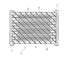
- FIG. 1 is a cross-sectional view of a multilayer ceramic capacitor according to an embodiment of the present invention.
- the dielectric composition according to this embodiment is Main component chemical formula (Sr 1.00-s-t Ba s Ca t) 6.00-x R x (Ti 1.00-a Zr a) x + 2.00 (Nb 1.00-b Ta b) 8.
- R is at least one element selected from Y, La, Pr, Nd, Sm, Eu, Gd, Tb, Dy, Ho, Er, Tm, Yb, and Lu;
- s, t, x, a, b are 0.70 ⁇ s ⁇ 1.00, 0 ⁇ t ⁇ 0.30, 0.70 ⁇ s + t ⁇ 1.00, 0 ⁇ x ⁇ 0.50, 0.10
- the dielectric composition according to the present embodiment is mainly composed of the tungsten bronze type complex oxide represented by the chemical formula
- a high withstand voltage can be easily obtained.
- the tungsten bronze complex oxide which is the main component of this embodiment, is characterized by a wide band gap. Therefore, electrons in the valence band are difficult to excite into the conduction band and are majority carriers involved in conduction. It becomes possible to suppress the electron carrier concentration.
- the carrier concentration of conduction electrons that are majority carriers may be affected.
- the dielectric composition of the present invention it is possible to suppress the carrier concentration of electrons, which are majority carriers, to be low, so that it is considered that breakdown due to avalanche is less likely to occur. Furthermore, since the band gap is wide, it is possible to maintain a wide band gap to some extent even when a high electric field strength is applied. Therefore, it seems that a high withstand voltage can be easily obtained even in a high electric field. In addition, since it does not contain an alkali metal, it is difficult to generate lattice defects and it is difficult to generate conduction electrons.
- a high withstand voltage can be easily obtained.
- higher withstand voltage can be obtained when s and t in the chemical formula are 0.80 ⁇ s ⁇ 1.00, 0 ⁇ t ⁇ 0.20, and 0.80 ⁇ s + t ⁇ 1.00. It becomes easy.
- K or Na which is an alkali metal element is included in addition to Sr, Ba, and Ca, since these elements have high volatility, lattice defects are generated, and as a result, it is difficult to obtain a high withstand voltage. It becomes.
- t represents the amount of substitution of Ca, but Ca is an arbitrary component, and the upper limit of the amount of substitution is 0.30.
- This octahedron has spontaneous polarization due to B site ions slightly shifted from the center position, and is inclined with respect to the c-axis direction. Then, it is considered that the octahedron is vibrated by the oscillating electric field, that is, the polarization is vibrated, and a higher dielectric constant is developed.
- X represents the amount of substitution of R, but R is an optional component, and the upper limit of the amount of substitution is 0.50.
- R in the chemical formula is at least one element selected from Y, La, Pr, Nd, Sm, Eu, Gd, Tb, Dy, Ho, Er, Tm, Yb, and Lu, and has high resistance even in a high temperature region. A voltage is easily obtained.
- x of the chemical formula is 0 ⁇ x ⁇ 0.50
- the x 0 (Sr 1.00-s -t Ba s Ca t) 6.00 (Ti 1.00-a Zr a) 2.00
- a tungsten bronze-type composite oxide such as (Nb 1.00-b Ta b ) 8.00 O 30.00
- a complex oxide such as a chemical formula Ba 5 LaTi 3 Nb 7 O 30 has a low relative dielectric constant at room temperature.
- the substitution amount a of Zr in the chemical formula is 0.10 ⁇ a ⁇ 1.00, the band gap is widened, so that a high withstand voltage is easily obtained.
- the substitution amount a is less than 0.10, it is difficult to widen the band gap, and as a result, it is difficult to obtain a high withstand voltage.
- the tungsten bronze-type crystal structure can be maintained, and the Ta substitution amount b is set to 0.10 ⁇ b ⁇ 1.00. High withstand voltage is easily obtained.
- At least one element selected from Mn, Mg, Co, V, W, Mo, Si, Li, B, and Al is included as a subcomponent.
- the interaction between these elements and Zr contained in the main component makes it easy to obtain a high specific resistance as well as a high withstand voltage.
- the substitution amount a of Zr is 0.80 ⁇ a ⁇ 1.00, the interaction is enhanced and a higher withstand voltage is easily obtained.
- a high specific resistance of 9.00 ⁇ 10 12 ⁇ cm or more can be obtained at 200 ° C. It becomes possible. Furthermore, a higher withstand voltage can be obtained even at a high temperature of 175 ° C. or higher.
- At least one selected from Y, La, Pr, Nd, Sm, Eu, Gd, Tb, Dy, Ho, Er, Tm, Yb, and Lu as the second subcomponent may be included.
- a 2nd subcomponent is arbitrary components, The upper limit of the content is determined in the range which can achieve the objective of invention.
- the dielectric composition may also contain minute impurities and other subcomponents as long as it does not significantly deteriorate the dielectric characteristics that are the effects of the present invention, that is, the relative permittivity, the specific resistance, and the withstand voltage. Absent. Therefore, the content of the main component is not particularly limited, but is, for example, 50 mol% or more and 100 mol% or less with respect to the entire dielectric composition containing the main component.
- FIG. 1 shows a multilayer ceramic capacitor according to an embodiment of the present invention.
- the multilayer ceramic capacitor 1 has a capacitor element body 10 having a configuration in which dielectric layers 2 and internal electrode layers 3 are alternately stacked. At both ends of the capacitor element body 10, a pair of external electrodes 4 are formed which are electrically connected to the internal electrode layers 3 arranged alternately in the element body 10.
- the shape of the capacitor element body 10 is not particularly limited, but is usually a rectangular parallelepiped shape. Moreover, there is no restriction
- the thickness of the dielectric layer 2 is not particularly limited, and may be appropriately determined according to the use of the multilayer ceramic capacitor 1.
- the conductive material contained in the internal electrode layer 3 is not particularly limited, but Ni, Pd, Ag, Pd—Ag alloy, Cu or Cu-based alloy is preferable.
- the Ni, Pd, Ag, Pd—Ag alloy, Cu, or Cu-based alloy may contain various trace components such as P of about 0.1% by weight or less.
- the internal electrode layer 3 may be formed using a commercially available electrode paste. What is necessary is just to determine the thickness of the internal electrode layer 3 suitably according to a use etc.
- a green chip is produced by a normal printing method or a sheet method using a paste as in the case of a conventional multilayer ceramic capacitor, fired, and then fired by applying an external electrode. It is manufactured by doing.
- the manufacturing method will be specifically described.
- a raw material is prepared so that a main component may become a desired ratio, it mixes, and a calcining powder can be obtained by heat-processing (temporary baking) at 800 degreeC or more.
- heat treatment is performed at 800 ° C. to 1000 ° C. so that the particle size of the calcined powder is 0.1 ⁇ m or more and 5.0 ⁇ m or less.
- a different phase such as Ba 5 Nb 4 O 15 having an anisotropic shape is not included in the calcined powder.
- an oxide mainly composed of Sr, Ba, Ca, Ti, Zr, Nb, and Ta or a mixture thereof can be used as the raw material powder.
- various compounds that become the above-described oxides or composite oxides by firing for example, carbonates, oxalates, nitrates, hydroxides, organometallic compounds, and the like can be appropriately selected and mixed for use.
- SrO may be used as a raw material for Sr, or SrCO 3 may be used.
- a raw material for the subcomponent is also prepared.
- the raw material of the subcomponent is not particularly limited, and an oxide of each component or a mixture thereof can be used as the raw material powder.
- various compounds that become the above-described oxides or composite oxides by firing for example, carbonates, oxalates, nitrates, hydroxides, organometallic compounds, and the like can be appropriately selected and mixed for use.
- MgO may be used as a raw material for Mg, or MgCO 3 may be used.
- Prepared calcined powder of main component and raw material of subcomponent are weighed and mixed so as to have a predetermined composition ratio to obtain a dielectric composition raw material.
- Examples of the mixing method include wet mixing using a ball mill and dry mixing using a dry mixer.
- This dielectric composition raw material is made into a paint to prepare a dielectric layer paste.
- the dielectric layer paste may be an organic paint obtained by kneading a dielectric material and an organic vehicle, or may be a water-based paint.
- Organic vehicle is a binder dissolved in an organic solvent.
- the binder used for the organic vehicle is not particularly limited, and may be appropriately selected from usual various binders such as ethyl cellulose and polyvinyl butyral.
- the organic solvent to be used is not particularly limited, and may be appropriately selected from various organic solvents such as terpineol, butyl carbitol, acetone and the like according to a method to be used such as a printing method or a sheet method.
- the dielectric layer paste when used as a water-based paint, a water-based vehicle in which a water-soluble binder or a dispersant is dissolved in water and a dielectric material may be kneaded.
- the water-soluble binder used for the water-based vehicle is not particularly limited, and for example, polyvinyl alcohol, cellulose, water-soluble acrylic resin, etc. may be used.
- the internal electrode layer paste is obtained by kneading the above-mentioned organic vehicle with various conductive metals and alloys as described above, or various oxides, organometallic compounds, resinates, etc. that become the above-mentioned conductive materials after firing. Prepare.
- the external electrode paste may be prepared in the same manner as the internal electrode layer paste described above.
- the content of the organic vehicle in each paste described above is not particularly limited, and may be a normal content, for example, about 1% to 5% by weight for the binder and about 10% to 50% by weight for the solvent.
- Each paste may contain additives selected from various dispersants, plasticizers, dielectric materials, insulator materials, and the like as necessary. The total content of these is preferably 10% by weight or less.
- the dielectric layer paste and the internal electrode layer paste are printed and laminated on a substrate such as PET, cut into a predetermined shape, and then peeled off from the substrate to obtain a green chip.
- a dielectric layer paste is used to form a green sheet, the internal electrode layer paste is printed thereon, and these are stacked to form a green chip.
- the temperature rising rate is preferably 5 ° C./hour to 300 ° C./hour
- the holding temperature is preferably 180 ° C. to 500 ° C.
- the temperature holding time is preferably 0.5 hours to 24 hours.
- the atmosphere for the binder removal treatment is air or a reducing atmosphere.
- the holding temperature during firing is preferably 1000 ° C. to 1400 ° C., more preferably 1100 ° C. to 1360 ° C. If the holding temperature is lower than the above range, the densification becomes insufficient. If the holding temperature exceeds the above range, the electrode is interrupted due to abnormal sintering of the internal electrode layer, or the capacity change rate is deteriorated due to diffusion of the constituent material of the internal electrode layer. It becomes easy. Moreover, when the said range is exceeded, there exists a possibility that a dielectric particle may coarsen and a withstand voltage may be reduced.
- the heating rate is preferably 50 ° C./hour to 500 ° C./hour, more preferably 200 ° C./hour to 300 ° C./hour, after sintering.
- the temperature holding time is preferably 0.5 hours to 24 hours, more preferably 1 hour to 3 hours
- the cooling rate is preferably 50 ° C. / Hour to 500 ° C./hour, more preferably 200 ° C./hour to 300 ° C./hour.
- a wetter or the like may be used to wet the N 2 gas, mixed gas, or the like.
- the water temperature is preferably about 5 to 75 ° C.
- the binder removal treatment, firing and annealing may be performed continuously or independently.
- the capacitor element body obtained as described above is subjected to end surface polishing by, for example, barrel polishing or sand blasting, and the external electrode paste is applied and baked to form the external electrode 4. Then, if necessary, a coating layer is formed on the surface of the external electrode 4 by plating or the like.
- SrCO 3 , BaCO 3 , CaCO 3 TiO 2 , ZrO 2 , Nb 2 O 5 , Ta 2 O 5 , Y 2 O 3 , La 2 O 3 , Pr 2 O 3 , Nd 2 O 3 , Sm 2 O 3 , Eu 2 O 3 , Gd 2 O 3 , Tb 2 O 3 , Dy 2 O 3 , Ho 2 O 3 , Er 2 O 3 , Tm 2 O 3 , Yb 2 O 3 , Lu 2 O 3 , Bi 2 O 3 powders were prepared.
- Dielectric composition raw material thus obtained 100 parts by weight, polyvinyl butyral resin: 10 parts by weight, dibutyl phthalate (DOP) as a plasticizer: 5 parts by weight, and alcohol as a solvent: 100 parts by weight
- DOP dibutyl phthalate
- alcohol as a solvent
- Pd particles 44.6 parts by weight, terpineol: 52 parts by weight, ethyl cellulose: 3 parts by weight, and benzotriazole: 0.4 parts by weight are kneaded by three rolls to form a slurry.
- a Pd internal electrode layer paste was produced.
- Ni internal electrode layer paste was prepared using Ni particles.
- a green sheet was formed on the PET film so that the thickness after drying was 7 ⁇ m.
- the internal electrode layer was printed in a predetermined pattern using the internal electrode layer paste thereon, and then the sheet was peeled from the PET film to produce a green sheet having the internal electrode layer.
- Sample No. 1 to sample no. Pd internal electrode layer paste was used for the green sheet using No. 60, and Sample No. 61 to sample no.
- the green sheets using 63 are made of Ni internal electrode layer paste to produce green sheets each having an internal electrode layer.
- a plurality of green sheets having internal electrode layers were laminated and pressure-bonded to form a green laminate, and the green laminate was cut into a predetermined size to obtain a green chip.
- the obtained green chip was subjected to binder removal treatment (temperature rising rate: 10 ° C./hour, holding temperature: 400 ° C., temperature holding time: 8 hours, atmosphere: in air), and fired (temperature rising rate: 200).
- binder removal treatment temperature rising rate: 10 ° C./hour, holding temperature: 400 ° C., temperature holding time: 8 hours, atmosphere: in air
- fired temperature rising rate: 200.
- an In—Ga eutectic alloy was applied as an external electrode, and a sample No. 1 having the same shape as the multilayer ceramic capacitor shown in FIG. 1 to sample no. 63 multilayer ceramic capacitors were obtained.
- the size of the obtained multilayer ceramic capacitor is 3.2 mm ⁇ 1.6 mm ⁇ 1.2 mm.
- the thickness of the dielectric layer is 5.0 ⁇ m, the thickness of the internal electrode layer is 1.5 ⁇ m, and it is sandwiched between the internal electrode layers.
- the number of dielectric layers was 10.
- Relative permittivity temperature change rate ⁇ ( ⁇ 200 ° C. ⁇ ⁇ 25 ° C. ) / ⁇ 25 ° C. ⁇ ⁇ 100 (1) In this example, it was determined that the relative permittivity change rate was within ⁇ 20%. .
- the insulation resistance of the multilayer ceramic capacitor sample was measured at 180 ° C. and 200 ° C. using a digital resistance meter (R8340 manufactured by ADVANTEST) under the conditions of a measurement voltage of 30 V and a measurement time of 60 seconds.
- the value of specific resistance was calculated from the electrode area of the capacitor sample and the thickness of the dielectric layer.
- the specific resistance is preferably as high as possible, and 1.00 ⁇ 10 12 ⁇ cm or more is more preferable, and 9.00 ⁇ 10 12 ⁇ cm or more is determined to be favorable. If the specific resistance is low, the leakage current of the capacitor becomes large, causing malfunction in the electric circuit.
- a DC voltage was applied to the multilayer ceramic capacitor sample at a boosting rate of 100 V / sec at 180 ° C. and 200 ° C., and the DC breakdown voltage was determined when the leakage current exceeded 10 mA.
- a higher DC withstand voltage is preferable, and it was determined that 150 V / ⁇ m or more, more preferably 155 V / ⁇ m or more, further preferably 160 V / ⁇ m or more, and particularly preferably 175 V / ⁇ m or more.
- a sample with * means that it is a comparative example.
- R is at least one element selected from Y, La, Pr, Nd, Sm, Eu, Gd, Tb, Dy, Ho, Er, Tm, Yb, and Lu
- s, t, x, a, b are 0.70 ⁇ s ⁇ 1.00, 0 ⁇ t ⁇ 0.30, 0.70 ⁇ s + t ⁇ 1.00, 0 ⁇ x ⁇ 0.50, 0.10
- the multilayer ceramic capacitor sample of this embodiment satisfying ⁇ a ⁇ 1.00 and 0 ⁇ b ⁇ 1.00 has a high relative dielectric constant of 500 or more at 25 ° C. and 200 ° C., and a specific resistance of 180 ° C. or more.
- a multilayer ceramic capacitor sample in which s, t and s + t do not satisfy 0.70 ⁇ s ⁇ 1.00, 0 ⁇ t ⁇ 0.30, and 0.70 ⁇ s + t ⁇ 1.00, respectively confirms that the relative dielectric constant at 25 ° C. and the relative dielectric constant at 200 ° C. are less than 500.
- the multilayer ceramic capacitor sample (Sample No. 11) in which the substitution amount x of R as the main component does not satisfy 0 ⁇ x ⁇ 0.50 has a relative dielectric constant of 25 ° C. And the relative dielectric constant at 200 ° C. is as low as less than 500.
- At least one element in which R as a main component is selected from Y, La, Pr, Nd, Sm, Eu, Gd, Tb, Dy, Ho, Er, Tm, Yb, and Lu.
- Multilayer ceramic capacitor samples (sample No. 1 to sample No. 8, sample No. 10 to sample No. 57 and sample No. 61 to sample No. 63) are the same as long as they are elements selected from the above. It was confirmed that the characteristics were exhibited.
- the multilayer ceramic capacitor samples (Sample No. 26 and Sample No. 55) in which the substitution amount a of Zr as the main component does not satisfy 0.10 ⁇ a ⁇ 1.00 are 200.
- the specific resistance at 0 ° C. is low, and the DC withstand voltage at 180 ° C. or higher is lowered.
- multilayer ceramic capacitor samples (sample No. 38 to sample No. 41) in which the molar amount of the subcomponent with respect to 100 mol of the main component is 0.10 mol ⁇ subcomponent ⁇ 20.00 mol are as follows: It was confirmed that the specific resistance at 200 ° C. was higher than 9.00 ⁇ 10 12 ⁇ cm and the DC withstand voltage at 200 ° C. was higher than 160 V / ⁇ m.
- a multilayer ceramic capacitor sample (sample No. 39, sample containing at least one selected from Mn, Mg, Co, V, W, Mo, Si, Li, B, and Al as subcomponents) No. 43 to Sample No. 51, Sample No. 53, Sample No. 54, Sample No. 56, and Sample No. 57) show 9.00 ⁇ 10 12 ⁇ cm or more with a higher specific resistance at 200 ° C.
- the DC withstand voltage at 200 ° C. is higher than 170 V / ⁇ m.
- the multilayer ceramic capacitor sample (sample No. 52) having Fe, which is an element other than the above-mentioned subcomponent, as a subcomponent has a specific resistance at 200 ° C.
- the subcomponent is preferably at least one selected from Mn, Mg, Co, V, W, Mo, Si, Li, B, and Al.
- the subcomponent contains at least one selected from Mn, Mg, Co, V, W, Mo, Si, Li, B, and Al, and the substitution amount a of Zr as the main component is 0.30 ⁇ a ⁇ 1 .00 sample No. 39 to sample no. 51 has a higher specific resistance and a higher withstand voltage.
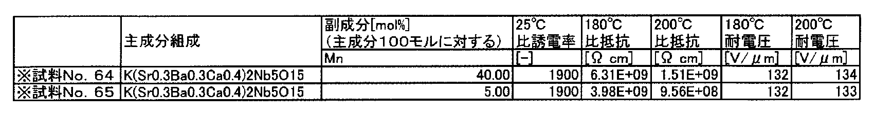
- tungsten bronze complex oxide K (Sr 0.3 Ba 0.3 Ca 0.4 ) 2 Nb 5 O 15 powder containing an alkali metal element synthesized in advance is prepared as a main component.
- MnCO 3 powder was prepared as a starting material for subcomponents to be added.
- MnCO 3 powder, which is a starting material of K (Sr 0.3 Ba 0.3 Ca 0.4 ) 2 Nb 5 O 15 powder, which is the main component, and subcomponents is weighed, and 100 mol of the main component is measured. Then, mixed powders were prepared by mixing so that the subcomponents had a predetermined ratio.
- the mixed powder of the main component and the subcomponent is used as the dielectric composition raw material.
- a dielectric layer paste was prepared in the same manner as in the example except that the dielectric composition raw material was used, and a green sheet was formed on the PET film so that the thickness after drying was 7 ⁇ m. Subsequently, the internal electrode layer was printed in a predetermined pattern using an internal electrode paste containing Ni as a main component thereon, and then the sheet was peeled from the PET film to produce a green sheet having the internal electrode layer. Subsequently, a green chip was obtained using a green sheet as in the example.
- the obtained green chip was subjected to binder removal treatment (temperature rising rate: 10 ° C./hour, holding temperature: 350 ° C., temperature holding time: 8 hours, atmosphere: in nitrogen), and fired (temperature rising rate: 200).
- ° C./hour holding temperature: 1100 ° C., temperature holding time: 2 hours, cooling rate: 200 ° C./hour , oxygen partial pressure: 10 ⁇ 9 to 10 ⁇ 12 Pa, atmosphere: H 2 —N 2 —H 2 O mixed Gas) to obtain a multilayer ceramic fired body.
- Sample No. which is a tungsten bronze type complex oxide containing an alkali metal element as a main component. 64 and sample no. It can be confirmed that No. 65 has low values of both withstand voltage and specific resistance because lattice defects due to alkali metal elements having high volatility are easily generated and conduction electrons are easily generated.
- the dielectric composition of the present invention has high DC withstand voltage and specific resistance in a high temperature region of 200 ° C., and also has a high relative dielectric constant, so that it can be applied as an in-vehicle electronic component in an environment close to an engine room. It can also be applied to applications as electronic components mounted near power devices using SiC or GaN-based semiconductors.
Landscapes
- Engineering & Computer Science (AREA)
- Chemical & Material Sciences (AREA)
- Ceramic Engineering (AREA)
- Manufacturing & Machinery (AREA)
- Power Engineering (AREA)
- Inorganic Chemistry (AREA)
- Organic Chemistry (AREA)
- Structural Engineering (AREA)
- Materials Engineering (AREA)
- Microelectronics & Electronic Packaging (AREA)
- Ceramic Capacitors (AREA)
- Inorganic Insulating Materials (AREA)
- Fixed Capacitors And Capacitor Manufacturing Machines (AREA)
Abstract
Description
また、揮発性の高いアルカリ金属を含むことにより、高温で熱処理を行う脱バインダ工程や焼成工程、再酸化工程で、誘電体組成物中にアルカリ金属に起因した格子欠陥が生成し易く、高い耐電圧が得られ難いという問題点があった。このため、前記特許文献1においては、高温領域において、高い比誘電率と高い耐電圧についての技術の開示はなされていない。
主成分が (Sr1.00-s-tBasCat)6.00-xRx(Ti1.00-aZra)x+2.00(Nb1.00-bTab)8.00-xO30.00で表され、
前記Rが
Y、La、Pr、Nd、Sm、Eu、Gd、Tb、Dy、Ho、Er、Tm、Yb、Luから選ばれる少なくとも一種の元素であり、
s、t、x、a、bが、0.70≦s≦1.00、0≦t≦0.30、0.70≦s+t≦1.00、0≦x≦0.50、0.10≦a≦1.00、0≦b≦1.00を満たすタングステンブロンズ型複合酸化物である主成分を有することを特徴とする。
主成分が 化学式(Sr1.00-s-tBasCat)6.00-xRx(Ti1.00-aZra)x+2.00(Nb1.00-bTab)8.00-xO30.00で表され、
前記Rが
Y、La、Pr、Nd、Sm、Eu、Gd、Tb、Dy、Ho、Er、Tm、Yb、Luから選ばれる少なくとも一種の元素であり、
s、t、x、a、bが、0.70≦s≦1.00、0≦t≦0.30、0.70≦s+t≦1.00、0≦x≦0.50、0.10≦a≦1.00、0≦b≦1.00を満たすタングステンブロンズ型複合酸化物である主成分を有することを特徴とする。

また、※印が付いている試料は比較例であることを意味している。
積層セラミックコンデンサに対し、25℃及び200℃において、デジタルLCRメータ(YHP社製4284A)にて、周波数1kHz、入力信号レベル(測定電圧)1Vrmsの信号を入力し、静電容量Cを測定した。そして、比誘電率εs(単位なし)を、誘電体層の厚みと、有効電極面積と、測定の結果得られた静電容量Cとに基づき算出した。比誘電率は高いほうが好ましく、500以上を良好であると判断した。また、25℃の比誘電率ε25℃に対する200℃の比誘電率ε200℃の変化率を式1に基づき算出した。
比誘電率温度変化率={(ε200℃-ε25℃)/ε25℃}×100 ・・・(1)本実施例では、比誘電率変化率が±20%以内を良好と判断した。
積層セラミックコンデンサ試料に対し、180℃、200℃において、デジタル抵抗メータ(ADVANTEST社製R8340)にて、測定電圧30V、測定時間60秒の条件で絶縁抵抗を測定した。コンデンサ試料の電極面積および誘電体層の厚みから比抵抗の値を算出した。比抵抗は高いほうが好ましく1.00×10¹²Ωcm以上より好ましくは9.00×10¹²Ωcm以上を良好であると判断した。比抵抗が低いとコンデンサとしては漏れ電流が大きくなり、電気回路において誤動作を起こしてしまう。
積層セラミックコンデンサ試料に対し、180℃、200℃において、100V/sec昇圧速度で直流電圧を印加し、漏れ電流が10mAを超えたところを直流耐電圧とした。直流耐電圧は高い方が好ましく、150V/μm以上、より好ましくは155V/μm以上、さらに好ましくは160V/μm以上、特に好ましくは175V/μm以上を良好であると判断した。

(比較例)
2 誘電体層
3 内部電極層
4 外部電極
10 コンデンサ素子本体
Claims (6)
- 主成分が化学式(Sr1.00-s-tBasCat)6.00-xRx(Ti1.00-aZra)x+2.00(Nb1.00-bTab)8.00-xO30.00で表され、
前記Rが
Y、La、Pr、Nd、Sm、Eu、Gd、Tb、Dy、Ho、Er、Tm、Yb、Luから選ばれる少なくとも一種の元素であり、s、t、x、a、bが、0.70≦s≦1.00、0≦t≦0.30、0.70≦s+t≦1.00、0≦x≦0.50、0.10≦a≦1.00、0≦b≦1.00を満たすタングステンブロンズ型複合酸化物である主成分を有する誘電体組成物。 - 前記主成分100モルに対して、副成分としてMn、Mg、Co、V、W、Mo、Si、Li、B、Alから選択される少なくとも一種を0.10モル以上20.00モル以下含むことを特徴とする請求項1に記載の誘電体組成物。
- 前記化学式中のZr置換量aが0.50≦a≦1.00であることを特徴とする請求項1記載の誘電体組成物。
- 請求項1~3のいずれかに記載の誘電体組成物を備える誘電体素子。
- 請求項1~3のいずれかに記載の誘電体組成物からなる誘電体層を備える電子部品。
- 請求項1~3のいずれかに記載の誘電体組成物からなる誘電体層と内部電極層とを交互に積層されてなる積層部分を有する積層電子部品。
Priority Applications (4)
| Application Number | Priority Date | Filing Date | Title |
|---|---|---|---|
| JP2018507184A JP6881433B2 (ja) | 2016-03-24 | 2017-03-06 | 誘電体組成物、誘電体素子、電子部品及び積層電子部品 |
| US16/087,790 US10777355B2 (en) | 2016-03-24 | 2017-03-06 | Dielectric composition, dielectric element, electronic component, and multilayer electronic component |
| CN201780019120.8A CN108883991B (zh) | 2016-03-24 | 2017-03-06 | 电介质组合物、电介质元件、电子部件及层叠电子部件 |
| EP17769887.5A EP3434657A4 (en) | 2016-03-24 | 2017-03-06 | DIELECTRIC COMPOSITION, DIELECTRIC ELEMENT, ELECTRONIC COMPONENT AND ELECTRONIC LAMINATE COMPONENT |
Applications Claiming Priority (2)
| Application Number | Priority Date | Filing Date | Title |
|---|---|---|---|
| JP2016-060421 | 2016-03-24 | ||
| JP2016060421 | 2016-03-24 |
Publications (1)
| Publication Number | Publication Date |
|---|---|
| WO2017163842A1 true WO2017163842A1 (ja) | 2017-09-28 |
Family
ID=59900114
Family Applications (1)
| Application Number | Title | Priority Date | Filing Date |
|---|---|---|---|
| PCT/JP2017/008802 Ceased WO2017163842A1 (ja) | 2016-03-24 | 2017-03-06 | 誘電体組成物、誘電体素子、電子部品及び積層電子部品 |
Country Status (5)
| Country | Link |
|---|---|
| US (1) | US10777355B2 (ja) |
| EP (1) | EP3434657A4 (ja) |
| JP (1) | JP6881433B2 (ja) |
| CN (1) | CN108883991B (ja) |
| WO (1) | WO2017163842A1 (ja) |
Cited By (6)
| Publication number | Priority date | Publication date | Assignee | Title |
|---|---|---|---|---|
| WO2019198419A1 (ja) * | 2018-04-11 | 2019-10-17 | 昭栄化学工業株式会社 | 誘電体磁器組成物及びセラミック電子部品 |
| WO2019198418A1 (ja) * | 2018-04-11 | 2019-10-17 | 昭栄化学工業株式会社 | 誘電体磁器組成物及びセラミック電子部品 |
| JP2020043310A (ja) * | 2018-09-13 | 2020-03-19 | Tdk株式会社 | 誘電体組成物および電子部品 |
| CN110894159A (zh) * | 2018-09-13 | 2020-03-20 | Tdk株式会社 | 电介质组合物及电子部件 |
| JP2020152622A (ja) * | 2019-03-22 | 2020-09-24 | Tdk株式会社 | 誘電体組成物および電子部品 |
| JP2024048975A (ja) * | 2022-09-28 | 2024-04-09 | Tdk株式会社 | 誘電体組成物および電子部品 |
Families Citing this family (5)
| Publication number | Priority date | Publication date | Assignee | Title |
|---|---|---|---|---|
| WO2017163842A1 (ja) * | 2016-03-24 | 2017-09-28 | Tdk株式会社 | 誘電体組成物、誘電体素子、電子部品及び積層電子部品 |
| CN108779031B (zh) * | 2016-03-24 | 2021-06-15 | Tdk株式会社 | 电介质组合物、电介质元件、电子部件及层叠电子部件 |
| EP3527546A4 (en) * | 2016-10-17 | 2020-10-07 | Shoei Chemical Inc. | COMPOSITION OF DIELECTRIC PORCELAIN AND ELECTRONIC CERAMIC COMPONENT |
| CN112341160B (zh) * | 2020-11-06 | 2022-08-30 | 南京工业大学 | 一种宽频高q低温度系数钡镁钙铌钽系复合陶瓷及其制备方法 |
| CN116844862B (zh) * | 2023-06-12 | 2024-02-09 | 潮州三环(集团)股份有限公司 | 一种电介质材料及其在制备陶瓷电容器中的应用 |
Citations (2)
| Publication number | Priority date | Publication date | Assignee | Title |
|---|---|---|---|---|
| JPH03274607A (ja) * | 1990-03-26 | 1991-12-05 | Toshiba Corp | 誘電体組成物 |
| CN102627471A (zh) * | 2012-04-11 | 2012-08-08 | 南京大学 | 多孔结构的Ba6Zr2Nb8O30陶瓷的制备方法 |
Family Cites Families (15)
| Publication number | Priority date | Publication date | Assignee | Title |
|---|---|---|---|---|
| CN1092391C (zh) * | 1994-10-19 | 2002-10-09 | Tdk株式会社 | 多层瓷介片状电容器 |
| JP3323801B2 (ja) | 1998-02-05 | 2002-09-09 | 太陽誘電株式会社 | 磁器コンデンサ |
| JP4407637B2 (ja) * | 2004-02-06 | 2010-02-03 | 株式会社村田製作所 | 強誘電体磁器組成物およびそれを用いた強誘電体応用素子 |
| JP5176543B2 (ja) | 2005-04-18 | 2013-04-03 | 株式会社村田製作所 | 積層セラミックコンデンサ |
| JP2007197277A (ja) * | 2006-01-27 | 2007-08-09 | Kyocera Corp | 誘電体磁器組成物および誘電体磁器、ならびにemiフィルタ |
| JP2007246340A (ja) * | 2006-03-16 | 2007-09-27 | Yokowo Co Ltd | 誘電体磁器組成物 |
| JP5564944B2 (ja) * | 2007-06-20 | 2014-08-06 | 株式会社村田製作所 | 誘電体セラミック組成物及び積層セラミックコンデンサ |
| CN101462878B (zh) * | 2008-12-31 | 2012-04-18 | 中国科学院上海硅酸盐研究所 | 声波测井系统多极子接收用压电陶瓷材料及其制备方法 |
| JP5835013B2 (ja) * | 2012-02-29 | 2015-12-24 | Tdk株式会社 | 誘電体磁器組成物および電子部品 |
| CN108779031B (zh) * | 2016-03-24 | 2021-06-15 | Tdk株式会社 | 电介质组合物、电介质元件、电子部件及层叠电子部件 |
| WO2017163842A1 (ja) * | 2016-03-24 | 2017-09-28 | Tdk株式会社 | 誘電体組成物、誘電体素子、電子部品及び積層電子部品 |
| EP3434659B1 (en) * | 2016-03-24 | 2021-08-11 | TDK Corporation | Dielectric composition, dielectric layer, electronic component and laminate electronic component |
| WO2017163843A1 (ja) * | 2016-03-24 | 2017-09-28 | Tdk株式会社 | 誘電体組成物、誘電体素子、電子部品及び積層電子部品 |
| JP2018104209A (ja) * | 2016-12-22 | 2018-07-05 | 株式会社村田製作所 | 誘電体磁器組成物および積層コンデンサ |
| US10354799B2 (en) * | 2017-02-23 | 2019-07-16 | Tdk Corporation | Dielectric composition, dielectric element, electronic device, and multilayer electronic device |
-
2017
- 2017-03-06 WO PCT/JP2017/008802 patent/WO2017163842A1/ja not_active Ceased
- 2017-03-06 CN CN201780019120.8A patent/CN108883991B/zh active Active
- 2017-03-06 JP JP2018507184A patent/JP6881433B2/ja active Active
- 2017-03-06 US US16/087,790 patent/US10777355B2/en active Active
- 2017-03-06 EP EP17769887.5A patent/EP3434657A4/en not_active Withdrawn
Patent Citations (2)
| Publication number | Priority date | Publication date | Assignee | Title |
|---|---|---|---|---|
| JPH03274607A (ja) * | 1990-03-26 | 1991-12-05 | Toshiba Corp | 誘電体組成物 |
| CN102627471A (zh) * | 2012-04-11 | 2012-08-08 | 南京大学 | 多孔结构的Ba6Zr2Nb8O30陶瓷的制备方法 |
Non-Patent Citations (3)
| Title |
|---|
| A PANIGRAHI: "Structural and electrical properties of Ba5RTi2ZrNb7030 [R=La, Nd, Sm, Eu, Gd, Dy] ceramic system", INDIAN JOURNAL OF PHYSICS , A, vol. 74A, no. 2, 2000, pages 147 - 149, XP009512753 * |
| See also references of EP3434657A4 * |
| ZHANG SHAN-TAO ET AL.: "Structural Evolving Sequence and Porous Ba6Zr2Nb8030 Ferroelectric Ceramics with Ultrahigh Breakdown Field and Zero Strain", JOURNAL OF AMERICAN CERAMIC SOCIETY, vol. 96, no. 2, February 2013 (2013-02-01), pages 555 - 560, XP055422640 * |
Cited By (16)
| Publication number | Priority date | Publication date | Assignee | Title |
|---|---|---|---|---|
| WO2019198419A1 (ja) * | 2018-04-11 | 2019-10-17 | 昭栄化学工業株式会社 | 誘電体磁器組成物及びセラミック電子部品 |
| WO2019198418A1 (ja) * | 2018-04-11 | 2019-10-17 | 昭栄化学工業株式会社 | 誘電体磁器組成物及びセラミック電子部品 |
| US11702368B2 (en) | 2018-04-11 | 2023-07-18 | Shoei Chemical Inc. | Dielectric ceramic composition and ceramic electronic component |
| JP7196906B2 (ja) | 2018-04-11 | 2022-12-27 | 昭栄化学工業株式会社 | 誘電体磁器組成物及びセラミック電子部品 |
| US11524923B2 (en) | 2018-04-11 | 2022-12-13 | Shoei Chemical Inc. | Dielectric ceramic composition and ceramic electronic components |
| JP7136196B2 (ja) | 2018-04-11 | 2022-09-13 | 昭栄化学工業株式会社 | 誘電体磁器組成物及びセラミック電子部品 |
| JPWO2019198419A1 (ja) * | 2018-04-11 | 2021-04-30 | 昭栄化学工業株式会社 | 誘電体磁器組成物及びセラミック電子部品 |
| JPWO2019198418A1 (ja) * | 2018-04-11 | 2021-05-27 | 昭栄化学工業株式会社 | 誘電体磁器組成物及びセラミック電子部品 |
| CN110894159B (zh) * | 2018-09-13 | 2022-03-01 | Tdk株式会社 | 电介质组合物及电子部件 |
| CN110894159A (zh) * | 2018-09-13 | 2020-03-20 | Tdk株式会社 | 电介质组合物及电子部件 |
| JP7196484B2 (ja) | 2018-09-13 | 2022-12-27 | Tdk株式会社 | 誘電体組成物および電子部品 |
| JP2020043310A (ja) * | 2018-09-13 | 2020-03-19 | Tdk株式会社 | 誘電体組成物および電子部品 |
| CN111718195A (zh) * | 2019-03-22 | 2020-09-29 | Tdk株式会社 | 电介质组合物和电子部件 |
| JP7168914B2 (ja) | 2019-03-22 | 2022-11-10 | Tdk株式会社 | 誘電体組成物および電子部品 |
| JP2020152622A (ja) * | 2019-03-22 | 2020-09-24 | Tdk株式会社 | 誘電体組成物および電子部品 |
| JP2024048975A (ja) * | 2022-09-28 | 2024-04-09 | Tdk株式会社 | 誘電体組成物および電子部品 |
Also Published As
| Publication number | Publication date |
|---|---|
| CN108883991A (zh) | 2018-11-23 |
| EP3434657A4 (en) | 2019-11-27 |
| CN108883991B (zh) | 2021-07-27 |
| EP3434657A1 (en) | 2019-01-30 |
| US10777355B2 (en) | 2020-09-15 |
| US20190115154A1 (en) | 2019-04-18 |
| JP6881433B2 (ja) | 2021-06-02 |
| JPWO2017163842A1 (ja) | 2019-03-14 |
Similar Documents
| Publication | Publication Date | Title |
|---|---|---|
| JP6809528B2 (ja) | 誘電体組成物、誘電体素子、電子部品及び積層電子部品 | |
| JP6881433B2 (ja) | 誘電体組成物、誘電体素子、電子部品及び積層電子部品 | |
| JP6801707B2 (ja) | 誘電体組成物、誘電体素子、電子部品及び積層電子部品 | |
| JP6973374B2 (ja) | 誘電体組成物、誘電体素子、電子部品及び積層電子部品 | |
| JP6696266B2 (ja) | 誘電体磁器組成物および積層セラミックコンデンサ | |
| JP4967965B2 (ja) | 誘電体磁器組成物および電子部品 | |
| US20120075768A1 (en) | Dielectric ceramic composition and manufacturing method thereof, and ceramic electronic device | |
| JP2011011918A (ja) | 誘電体セラミックおよびその製造方法ならびに積層セラミックコンデンサ | |
| TWI734892B (zh) | 積層陶瓷電容器及其製造方法 | |
| JP5685931B2 (ja) | 積層セラミックコンデンサ | |
| JP2011057511A (ja) | セラミック電子部品およびその製造方法 | |
| JP2004292173A (ja) | 非還元性誘電体セラミックおよびその製造方法ならびに積層セラミックコンデンサ | |
| JP2014162679A (ja) | 誘電体磁器組成物および電子部品 | |
| JP6696267B2 (ja) | 誘電体磁器組成物および積層セラミックコンデンサ | |
| JP2019099427A (ja) | 誘電体組成物、電子部品および積層電子部品 | |
| JPWO2009041160A1 (ja) | 誘電体セラミック及び積層セラミックコンデンサ | |
| JP2013211398A (ja) | 積層セラミックコンデンサ | |
| JP4863007B2 (ja) | 誘電体磁器組成物および電子部品 | |
| JP4853360B2 (ja) | 誘電体磁器組成物および電子部品 | |
| JP6376001B2 (ja) | 誘電体組成物 | |
| JP5146492B2 (ja) | 誘電体磁器組成物およびその製造方法 | |
| JP5471687B2 (ja) | 誘電体磁器組成物および電子部品 | |
| JP2016160132A (ja) | 誘電体組成物及び電子部品 |
Legal Events
| Date | Code | Title | Description |
|---|---|---|---|
| WWE | Wipo information: entry into national phase |
Ref document number: 2018507184 Country of ref document: JP |
|
| NENP | Non-entry into the national phase |
Ref country code: DE |
|
| WWE | Wipo information: entry into national phase |
Ref document number: 2017769887 Country of ref document: EP |
|
| ENP | Entry into the national phase |
Ref document number: 2017769887 Country of ref document: EP Effective date: 20181024 |
|
| 121 | Ep: the epo has been informed by wipo that ep was designated in this application |
Ref document number: 17769887 Country of ref document: EP Kind code of ref document: A1 |