WO2017163971A1 - Feuille de support et feuille composite pour une formation de film de protection - Google Patents
Feuille de support et feuille composite pour une formation de film de protection Download PDFInfo
- Publication number
- WO2017163971A1 WO2017163971A1 PCT/JP2017/009921 JP2017009921W WO2017163971A1 WO 2017163971 A1 WO2017163971 A1 WO 2017163971A1 JP 2017009921 W JP2017009921 W JP 2017009921W WO 2017163971 A1 WO2017163971 A1 WO 2017163971A1
- Authority
- WO
- WIPO (PCT)
- Prior art keywords
- protective film
- forming
- adhesive layer
- film
- meth
- Prior art date
- Legal status (The legal status is an assumption and is not a legal conclusion. Google has not performed a legal analysis and makes no representation as to the accuracy of the status listed.)
- Ceased
Links
Images


Classifications
-
- B—PERFORMING OPERATIONS; TRANSPORTING
- B32—LAYERED PRODUCTS
- B32B—LAYERED PRODUCTS, i.e. PRODUCTS BUILT-UP OF STRATA OF FLAT OR NON-FLAT, e.g. CELLULAR OR HONEYCOMB, FORM
- B32B5/00—Layered products characterised by the non- homogeneity or physical structure, i.e. comprising a fibrous, filamentary, particulate or foam layer; Layered products characterised by having a layer differing constitutionally or physically in different parts
- B32B5/14—Layered products characterised by the non- homogeneity or physical structure, i.e. comprising a fibrous, filamentary, particulate or foam layer; Layered products characterised by having a layer differing constitutionally or physically in different parts characterised by a layer differing constitutionally or physically in different parts, e.g. denser near its faces
- B32B5/145—Variation across the thickness of the layer
-
- B—PERFORMING OPERATIONS; TRANSPORTING
- B32—LAYERED PRODUCTS
- B32B—LAYERED PRODUCTS, i.e. PRODUCTS BUILT-UP OF STRATA OF FLAT OR NON-FLAT, e.g. CELLULAR OR HONEYCOMB, FORM
- B32B27/00—Layered products comprising a layer of synthetic resin
-
- B—PERFORMING OPERATIONS; TRANSPORTING
- B32—LAYERED PRODUCTS
- B32B—LAYERED PRODUCTS, i.e. PRODUCTS BUILT-UP OF STRATA OF FLAT OR NON-FLAT, e.g. CELLULAR OR HONEYCOMB, FORM
- B32B27/00—Layered products comprising a layer of synthetic resin
- B32B27/06—Layered products comprising a layer of synthetic resin as the main or only constituent of a layer, which is next to another layer of the same or of a different material
- B32B27/08—Layered products comprising a layer of synthetic resin as the main or only constituent of a layer, which is next to another layer of the same or of a different material of synthetic resin
-
- B—PERFORMING OPERATIONS; TRANSPORTING
- B32—LAYERED PRODUCTS
- B32B—LAYERED PRODUCTS, i.e. PRODUCTS BUILT-UP OF STRATA OF FLAT OR NON-FLAT, e.g. CELLULAR OR HONEYCOMB, FORM
- B32B27/00—Layered products comprising a layer of synthetic resin
- B32B27/18—Layered products comprising a layer of synthetic resin characterised by the use of special additives
- B32B27/20—Layered products comprising a layer of synthetic resin characterised by the use of special additives using fillers, pigments, thixotroping agents
-
- B—PERFORMING OPERATIONS; TRANSPORTING
- B32—LAYERED PRODUCTS
- B32B—LAYERED PRODUCTS, i.e. PRODUCTS BUILT-UP OF STRATA OF FLAT OR NON-FLAT, e.g. CELLULAR OR HONEYCOMB, FORM
- B32B27/00—Layered products comprising a layer of synthetic resin
- B32B27/30—Layered products comprising a layer of synthetic resin comprising vinyl (co)polymers; comprising acrylic (co)polymers
- B32B27/308—Layered products comprising a layer of synthetic resin comprising vinyl (co)polymers; comprising acrylic (co)polymers comprising acrylic (co)polymers
-
- B—PERFORMING OPERATIONS; TRANSPORTING
- B32—LAYERED PRODUCTS
- B32B—LAYERED PRODUCTS, i.e. PRODUCTS BUILT-UP OF STRATA OF FLAT OR NON-FLAT, e.g. CELLULAR OR HONEYCOMB, FORM
- B32B27/00—Layered products comprising a layer of synthetic resin
- B32B27/32—Layered products comprising a layer of synthetic resin comprising polyolefins
-
- B—PERFORMING OPERATIONS; TRANSPORTING
- B32—LAYERED PRODUCTS
- B32B—LAYERED PRODUCTS, i.e. PRODUCTS BUILT-UP OF STRATA OF FLAT OR NON-FLAT, e.g. CELLULAR OR HONEYCOMB, FORM
- B32B27/00—Layered products comprising a layer of synthetic resin
- B32B27/38—Layered products comprising a layer of synthetic resin comprising epoxy resins
-
- B—PERFORMING OPERATIONS; TRANSPORTING
- B32—LAYERED PRODUCTS
- B32B—LAYERED PRODUCTS, i.e. PRODUCTS BUILT-UP OF STRATA OF FLAT OR NON-FLAT, e.g. CELLULAR OR HONEYCOMB, FORM
- B32B3/00—Layered products comprising a layer with external or internal discontinuities or unevennesses, or a layer of non-planar shape; Layered products comprising a layer having particular features of form
- B32B3/26—Layered products comprising a layer with external or internal discontinuities or unevennesses, or a layer of non-planar shape; Layered products comprising a layer having particular features of form characterised by a particular shape of the outline of the cross-section of a continuous layer; characterised by a layer with cavities or internal voids ; characterised by an apertured layer
- B32B3/30—Layered products comprising a layer with external or internal discontinuities or unevennesses, or a layer of non-planar shape; Layered products comprising a layer having particular features of form characterised by a particular shape of the outline of the cross-section of a continuous layer; characterised by a layer with cavities or internal voids ; characterised by an apertured layer characterised by a layer formed with recesses or projections, e.g. hollows, grooves, protuberances, ribs
-
- B—PERFORMING OPERATIONS; TRANSPORTING
- B32—LAYERED PRODUCTS
- B32B—LAYERED PRODUCTS, i.e. PRODUCTS BUILT-UP OF STRATA OF FLAT OR NON-FLAT, e.g. CELLULAR OR HONEYCOMB, FORM
- B32B7/00—Layered products characterised by the relation between layers; Layered products characterised by the relative orientation of features between layers, or by the relative values of a measurable parameter between layers, i.e. products comprising layers having different physical, chemical or physicochemical properties; Layered products characterised by the interconnection of layers
- B32B7/04—Interconnection of layers
- B32B7/06—Interconnection of layers permitting easy separation
-
- B—PERFORMING OPERATIONS; TRANSPORTING
- B32—LAYERED PRODUCTS
- B32B—LAYERED PRODUCTS, i.e. PRODUCTS BUILT-UP OF STRATA OF FLAT OR NON-FLAT, e.g. CELLULAR OR HONEYCOMB, FORM
- B32B7/00—Layered products characterised by the relation between layers; Layered products characterised by the relative orientation of features between layers, or by the relative values of a measurable parameter between layers, i.e. products comprising layers having different physical, chemical or physicochemical properties; Layered products characterised by the interconnection of layers
- B32B7/04—Interconnection of layers
- B32B7/12—Interconnection of layers using interposed adhesives or interposed materials with bonding properties
-
- C—CHEMISTRY; METALLURGY
- C09—DYES; PAINTS; POLISHES; NATURAL RESINS; ADHESIVES; COMPOSITIONS NOT OTHERWISE PROVIDED FOR; APPLICATIONS OF MATERIALS NOT OTHERWISE PROVIDED FOR
- C09J—ADHESIVES; NON-MECHANICAL ASPECTS OF ADHESIVE PROCESSES IN GENERAL; ADHESIVE PROCESSES NOT PROVIDED FOR ELSEWHERE; USE OF MATERIALS AS ADHESIVES
- C09J201/00—Adhesives based on unspecified macromolecular compounds
-
- C—CHEMISTRY; METALLURGY
- C09—DYES; PAINTS; POLISHES; NATURAL RESINS; ADHESIVES; COMPOSITIONS NOT OTHERWISE PROVIDED FOR; APPLICATIONS OF MATERIALS NOT OTHERWISE PROVIDED FOR
- C09J—ADHESIVES; NON-MECHANICAL ASPECTS OF ADHESIVE PROCESSES IN GENERAL; ADHESIVE PROCESSES NOT PROVIDED FOR ELSEWHERE; USE OF MATERIALS AS ADHESIVES
- C09J7/00—Adhesives in the form of films or foils
- C09J7/20—Adhesives in the form of films or foils characterised by their carriers
-
- B—PERFORMING OPERATIONS; TRANSPORTING
- B32—LAYERED PRODUCTS
- B32B—LAYERED PRODUCTS, i.e. PRODUCTS BUILT-UP OF STRATA OF FLAT OR NON-FLAT, e.g. CELLULAR OR HONEYCOMB, FORM
- B32B2270/00—Resin or rubber layer containing a blend of at least two different polymers
-
- B—PERFORMING OPERATIONS; TRANSPORTING
- B32—LAYERED PRODUCTS
- B32B—LAYERED PRODUCTS, i.e. PRODUCTS BUILT-UP OF STRATA OF FLAT OR NON-FLAT, e.g. CELLULAR OR HONEYCOMB, FORM
- B32B2307/00—Properties of the layers or laminate
- B32B2307/50—Properties of the layers or laminate having particular mechanical properties
- B32B2307/538—Roughness
Definitions
- the present invention relates to a support sheet and a composite sheet for forming a protective film.
- semiconductor devices have been manufactured using a mounting method called a so-called face down method.
- a semiconductor chip having electrodes such as bumps on a circuit surface is used, and the electrodes are bonded to a substrate. For this reason, the back surface opposite to the circuit surface of the semiconductor chip may be exposed.
- a resin film made of an organic material is formed as a protective film on the exposed back surface of the semiconductor chip, and the semiconductor chip with the protective film obtained by forming the protective film in this way is taken into the semiconductor device. There is.
- the protective film is used to prevent so-called chipping in which cracks and chips are generated in the semiconductor chip in the steps after the dicing step.
- a protective film-forming composite sheet comprising a protective film-forming film (protective film-forming layer) on a support sheet.
- a support sheet for example, a laminated sheet in which an adhesive layer or the like is laminated on a resin base material is used.
- the support sheet in addition to the protective film-forming film having a protective film-forming ability, the support sheet can function as a dicing sheet, and the protective film-forming film and the dicing sheet are integrated. It can be made.
- surface or both surfaces have uneven
- the base material before processing, the support sheet obtained using this base material, or the composite sheet for forming a protective film is rolled up to form a roll. ),
- the contact surfaces of the rolls stick together and block, making it difficult to use.
- the contact surface is each surface of the substrate in the case of a roll of a substrate, and in the case of a composite sheet for forming a support sheet and a protective film, the exposed surface of the substrate that is the lowermost layer. It is the exposed surface of the uppermost layer such as a release film.
- the sheet is wrinkled, or the uppermost layer (usually a release film) is peeled off from the sheet when the sheet is unwound from the roll.
- the uppermost layer usually a release film
- laser printing is performed on the surface of the protective film attached to the semiconductor wafer or the semiconductor chip on the support sheet side by irradiation with laser light (referred to as “laser printing” in this specification). May be performed).
- the laser light is irradiated through the support sheet from the side opposite to the side where the protective film of the support sheet (base material) is formed. That is, the laser light enters the support sheet from the exposed surface side of the base material and reaches the protective film. Therefore, when the exposed surface of the substrate is an uneven surface, the laser light is irregularly reflected here, and there is a problem that the laser printing may become unclear.
- the state of a protective film forming composite sheet or a semiconductor wafer or a semiconductor chip provided with a protective film may be inspected by an infrared camera or the like through the sheet or the like.
- an infrared camera or the like may be inspected by an infrared camera or the like through the sheet or the like.
- the laser light is irregularly reflected on the exposed surface of the substrate as described above, there is a problem that a clear inspection image cannot be obtained.
- a base film having a concavo-convex surface only on one side is used, and the concavo-convex surface is not an exposed surface, and the protective film A film (dicing tape-integrated semiconductor back surface protective film) disposed toward the forming film side is disclosed (see Patent Document 1).
- the haze of a laminated sheet (dicing tape) formed by laminating a base material and an adhesive layer is 45% or less.
- the composite sheet for forming a protective film disclosed in Patent Document 1 has a problem in that the above-described blocking cannot be suppressed when the roll is rolled up because the exposed surface of the base material is a smooth surface. . Furthermore, when an adhesive layer is provided on the uneven surface of the substrate, the adhesive layer needs to be soft and thick enough to reduce the effect of the uneven surface on the adhesive layer. There was a problem. If the pressure-sensitive adhesive layer is hard, a portion of the base material surface near the base of the convex portion is not filled with the pressure-sensitive adhesive layer, and a void may occur.
- the surface on the substrate side (back surface) of the protective film-forming film becomes an uneven surface reflecting the uneven shape on the surface of the substrate.
- the protective film is formed from a film for forming a protective film that has a problem that the embedding of the uneven shape on the surface of the substrate is insufficient, and the laser printing is performed on the surface on the support sheet side, the printing becomes unclear. turn into. In addition, a clear inspection image of the semiconductor wafer or semiconductor chip cannot be acquired.
- the pressure-sensitive adhesive layer is too thick, for example, the pressure-sensitive adhesive layer being cut in the dicing process is likely to vibrate, so that the semiconductor chip and the semiconductor wafer being cut in the process of becoming a semiconductor chip also vibrate. There is also a problem that an extra force is applied to these semiconductor chips and semiconductor wafers, and as a result, the semiconductor chips are easily cracked and chipped (chipping is likely to occur).
- the present invention relates to suppression of blocking, clear laser printing on a protective film, and a semiconductor wafer or semiconductor chip without causing problems such as insufficient embedding of the base material surface with an adhesive layer and occurrence of chipping.
- An object of the present invention is to provide a composite sheet for forming a protective film that enables all of the clear inspection images to be obtained, and a support sheet used for manufacturing the composite sheet for forming the protective film.
- the present invention includes a base material and a pressure-sensitive adhesive layer laminated on the base material, and the surface roughness (Ra) on the surface of the base material on the side including the pressure-sensitive adhesive layer is 0. 4 ⁇ m or less, and the surface roughness (Ra) on the surface of the substrate opposite to the side provided with the pressure-sensitive adhesive layer is larger than the surface roughness on the surface provided with the pressure-sensitive adhesive layer.
- a support sheet that is large and has a size of 0.053 to 0.48 ⁇ m is provided.
- the pressure-sensitive adhesive layer may have a thickness of 15 ⁇ m or less.
- the pressure-sensitive adhesive layer may be non-energy ray curable.
- this invention provides the composite sheet for protective film formation provided with the said support sheet, and further provided with the film for protective film formation on the said adhesive layer in the said support sheet.
- the support sheet and the protective film-forming composite sheet of the present invention By using the support sheet and the protective film-forming composite sheet of the present invention, the embedding of the surface of the base material with the pressure-sensitive adhesive layer becomes insufficient, and the occurrence of chipping is prevented. It is possible to perform clear laser printing on the wafer and acquisition of a clear inspection image of the semiconductor wafer or semiconductor chip.
- the support sheet of the present invention includes a base material and an adhesive layer laminated on the base material, and includes the adhesive layer of the base material.
- the surface roughness (Ra) of the surface on the side (hereinafter sometimes referred to as “first surface”) is 0.4 ⁇ m or less, and the side of the substrate opposite to the side provided with the pressure-sensitive adhesive layer
- the surface roughness (Ra) on the surface (hereinafter sometimes referred to as “second surface”) is larger than the surface roughness on the surface (first surface) provided with the pressure-sensitive adhesive layer, and 0 .053 to 0.48 ⁇ m.
- the support sheet is for constituting the following protective film forming composite sheet, and can be used as a semiconductor wafer processing sheet such as a dicing sheet.
- the surface having a smaller surface roughness (for example, the surface having a surface roughness of 0.4 ⁇ m or less, the first surface) of both surfaces of the substrate is referred to as a smooth surface.
- a surface having a larger surface roughness (for example, a surface having a surface roughness of 0.053 to 0.48 ⁇ m, a second surface) may be referred to as an uneven surface. That is, the names “smooth surface” and “uneven surface” of the base material do not necessarily represent the absolute smoothness of these surfaces, but represent the relative magnitude of the relative smoothness of these surfaces.
- the composite sheet for protective film formation of this invention is equipped with the said support sheet, and is further provided with the film for protective film formation on the said adhesive layer in the said support sheet.
- the surface roughness of the first surface and the second surface is within a specific range as the base material, and the surface roughness of the second surface is more than the surface roughness of the first surface.
- the composite sheet for forming a protective film has a surface roughness of the first surface of the base material within a specific range (small value), and has a low degree of unevenness, thereby softening the adhesive layer. Therefore, it is not necessary to make it sufficiently thick, and the occurrence of problems such as insufficient embedding of the first surface of the base material by the adhesive layer and occurrence of chipping can be suppressed.
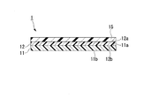
- FIG. 1 is a cross-sectional view schematically showing an embodiment of the support sheet of the present invention.
- the support sheet 1 shown here includes an adhesive layer 12 on a base material 11, and further includes a release film 15 on the adhesive layer 12.
- a pressure-sensitive adhesive layer 12 is laminated on one surface (first surface) 11a of the base material 11, and the other surface of the base material 11, that is, the side opposite to the side having the pressure-sensitive adhesive layer 12 is provided.
- the surface (second surface) 11b is an exposed surface.
- the first surface 11 a has a surface roughness of 0.4 ⁇ m or less
- the second surface 11 b has a surface roughness larger than the surface roughness of the first surface 11 a and 0.053. 0.48 ⁇ m.
- surface roughness means a so-called arithmetic average roughness obtained in accordance with JIS B0601: 2001, and is abbreviated as “Ra” unless otherwise specified.
- the release film 15 is here.
- first surface 12 a On one surface of the pressure-sensitive adhesive layer 12, that is, on the surface opposite to the side on which the substrate 11 is provided (hereinafter sometimes referred to as “first surface”) 12 a, the release film 15 is here.
- symbol 12b means the other surface of the adhesive layer 12, ie, the surface (the following may be called "the 2nd surface") by which the base material 11 is provided.
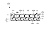
- FIG. 2 is a cross-sectional view schematically showing one embodiment of the composite sheet for forming a protective film of the present invention.
- the protective film-forming composite sheet 101 shown here includes an adhesive layer 12 on a base material 11 and a protective film-forming film 13 on the adhesive layer 12.
- the protective sheet-forming composite sheet 101 can be configured using the support sheet 1, and it can be said that the protective film-forming film 13 is further provided on the pressure-sensitive adhesive layer 12 in the support sheet 1.
- the protective film forming film 13 is laminated on the entire first surface 12 a of the pressure-sensitive adhesive layer 12.
- first surface 13a a part of the surface 13a opposite to the side on which the pressure-sensitive adhesive layer 12 of the protective film-forming film 13 is provided (hereinafter sometimes referred to as “first surface”) 13a, that is, in the vicinity of the periphery In the region, a jig adhesive layer 14 is laminated.
- first surface 13 a of the protective film forming film 13 the surface on which the jig adhesive layer 14 is not laminated is not in contact with the protective film forming film 13 of the jig adhesive layer 14.
- a release film 15 is laminated on the surface (first surface 14a and side surface 14c).
- the first surface 14a of the jig adhesive layer 14 is a surface opposite to the side of the jig adhesive layer 14 that is in contact with the protective film forming film 13, and is used for the jig. In some cases, the boundary between the first surface 14a and the side surface 14c of the adhesive layer 14 cannot be clearly distinguished. Further, the release film 15 may not be in contact with the side surface 14c of the jig adhesive layer 14.
- the protective sheet-forming composite sheet 1 is usually stored in a state in which the release film 15 is provided as described above.
- reference numeral 15 a indicates the surface of the release film 15 opposite to the side in contact with the protective film-forming film 13 (hereinafter sometimes referred to as “first surface”). .
- the protective film-forming composite sheet 101 is a surface on which a circuit of a semiconductor wafer (not shown) is formed by the first surface 13a of the protective film-forming film 13 with the release film 15 removed (this specification). Is affixed to a surface opposite to the “circuit forming surface” (which may be abbreviated as “back surface” in this specification), and The first surface 14a is used by being attached to a jig such as a ring frame.
- the second surface 11b of the substrate 11 has a surface roughness of 0.053 to 0.48 ⁇ m, and this surface roughness is equal to that of the first surface 11a of the substrate 11. It is larger than the surface roughness and has an appropriate uneven shape.
- the protective film forming film 13 is applied to the surface (back surface) opposite to the circuit forming surface of the semiconductor wafer or semiconductor chip, it is made into a protective film by curing.
- Printing may be performed by irradiation of laser light from the second surface 11b side of the substrate 11. At this time, the laser light enters the support sheet 1 from the second surface 11b side of the substrate 11 and reaches the protective film. Therefore, as described above, the second surface 11b of the substrate 11 has an appropriate uneven shape, and the irregularity is low, so that the irregular reflection of the laser light on the second surface 11b of the substrate 11 is suppressed, and the protective film is formed. Clear laser printing is possible.
- the protective film forming composite sheet 101 or the semiconductor wafer or semiconductor chip provided with the protective film is inspected by an infrared camera or the like through the protective film forming composite sheet 101 or the protective film.
- the second surface 11b of the base material 11 has an appropriate uneven shape, and the irregularity is low, so that irregular reflection of infrared rays on the second surface 11b of the base material 11 is suppressed, and a clear inspection is performed. Images can be acquired.
- the pressure-sensitive adhesive is used to reduce the influence of the uneven surface on the pressure-sensitive adhesive layer.
- the layer should be soft and thick enough. This is because when the pressure-sensitive adhesive layer is hard, the pressure-sensitive adhesive layer may not be filled in the vicinity of the base of the convex portion on the surface of the base material, and a void may be formed. This is because the surface (back surface) on the substrate side of the protective film-forming film becomes an uneven surface reflecting the uneven shape on the surface.
- the first surface 11a of the substrate 11 on which the pressure-sensitive adhesive layer 12 is provided has a surface roughness of 0.4 ⁇ m or less and high smoothness ( Since the unevenness is low), the above-described problems can be avoided. That is, in the protective film-forming composite sheet 101, the first surface 11a of the substrate 11 can be sufficiently embedded with the pressure-sensitive adhesive layer 12, and it is not necessary to form the pressure-sensitive adhesive layer 12 thick. Can be suppressed.
- FIG. 3 is a cross-sectional view schematically showing another embodiment of the composite sheet for forming a protective film of the present invention.
- the protective film-forming composite sheet 102 shown here is the same as the protective film-forming composite sheet 101 shown in FIG. 2 except that the shape of the protective film-forming film is different and the jig adhesive layer is not provided. It is. That is, the protective film-forming composite sheet 102 includes the adhesive layer 12 on the base material 11, the protective film-forming film 23 on the adhesive layer 12, and the protective film-forming film 23 on the protective film-forming film 23. A release film 15 is provided.
- the protective film-forming film 23 is laminated on a part of the first surface 12 a of the pressure-sensitive adhesive layer 12, that is, a region on the center side in the width direction (left-right direction in FIG. 3) of the support sheet 1.
- the first surface 12 a of the pressure-sensitive adhesive layer 12 the surface on which the protective film-forming film 23 is not laminated and the surface of the protective film-forming film 23 that is not in contact with the pressure-sensitive adhesive layer 12 (first surface 23 a Further, the release film 15 is laminated on the side surface 23c).
- the first surface 23a of the protective film-forming film 23 is a surface opposite to the side in contact with the pressure-sensitive adhesive layer 12 of the protective film-forming film 23.
- the boundary between the first surface 23a and the side surface 23c cannot be clearly distinguished. Further, the release film 15 may not be in contact with the side surface 23 c of the protective film forming film 23.
- the composite sheet 102 for forming a protective film is usually stored with the release film 15 as described above.
- the protective film-forming composite sheet 102 is attached to the back surface of the semiconductor wafer (not shown) by the first surface 23a of the protective film-forming film 23 with the release film 15 removed, and further, the adhesive layer 12 Of the first surface 12a, the surface on which the protective film forming film 23 is not laminated is attached to a jig such as a ring frame and used.
- the protective sheet-forming composite sheet 102 also has a surface roughness of the first surface 11a of the substrate 11 of 0.4 ⁇ m or less, and the surface roughness of the second surface 11b is larger than the surface roughness of the first surface 11a. And 0.053 to 0.48 ⁇ m.
- the protective film-forming composite sheet 102 as in the case of the protective film-forming composite sheet 101, is insufficiently embedded in the first surface 11a of the base material 11 by the adhesive layer 12, and It is possible to suppress blocking, obtain clear laser printing on a protective film, and obtain a clear inspection image of a semiconductor wafer or semiconductor chip without causing any defects.
- FIG. 4 is a cross-sectional view schematically showing still another embodiment of the composite sheet for forming a protective film of the present invention.
- the protective film-forming composite sheet 103 shown here is further provided for the jig on the surface of the first surface 12a of the pressure-sensitive adhesive layer 12 where the protective film-forming film 23 is not laminated, that is, in the vicinity of the peripheral edge. Except that the adhesive layer 14 is laminated, it is the same as the composite sheet 102 for forming a protective film shown in FIG.
- the protective film-forming composite sheet 103 is attached to the back surface of the semiconductor wafer (not shown) by the first surface 23a of the protective film-forming film 23 in a state where the release film 15 is removed.
- the first surface 14a of the agent layer 14 is used by being attached to a jig such as a ring frame.
- the protective sheet-forming composite sheet 103 also has a surface roughness of the first surface 11a of the substrate 11 of 0.4 ⁇ m or less, and the surface roughness of the second surface 11b is larger than the surface roughness of the first surface 11a. And 0.053 to 0.48 ⁇ m.
- the protective film-forming composite sheet 103 is not sufficiently embedded in the first surface 11a of the base material 11 by the pressure-sensitive adhesive layer 12, as in the case of the protective film-forming composite sheet 101. It is possible to suppress blocking, obtain clear laser printing on a protective film, and obtain a clear inspection image of a semiconductor wafer or semiconductor chip without causing any defects.
- the composite sheet for forming a protective film of the present invention is not limited to the one shown in FIGS. 2 to 4, and a part of the structure shown in FIGS. In addition, another configuration may be added to what has been described so far. Next, the structure of each layer of the support sheet and the composite sheet for forming a protective film of the present invention will be described.
- the surface roughness of the base material on the side (first surface) provided with the pressure-sensitive adhesive layer is 0.4 ⁇ m or less, for example, 0.37 ⁇ m or less, 0.3 ⁇ m or less, 0 .2 ⁇ m or less, 0.1 ⁇ m or less, 0.09 ⁇ m or less, 0.08 ⁇ m or less, 0.07 ⁇ m or less, or 0.06 ⁇ m or less, etc., but these are only examples.
- the lower limit value of the surface roughness on the first surface of the substrate is not particularly limited, and may be 0.01 ⁇ m, for example, but this is an example.
- Preferred examples of the surface roughness on the first surface include 0.01 to 0.4 ⁇ m, 0.01 to 0.37 ⁇ m, 0.01 to 0.3 ⁇ m, 0.01 to 0.2 ⁇ m, and 0.01 to Examples thereof include 0.1 ⁇ m, 0.01 to 0.09 ⁇ m, 0.01 to 0.08 ⁇ m, 0.01 to 0.07 ⁇ m, and 0.01 to 0.06 ⁇ m.
- the surface roughness of the surface (second surface) on the side opposite to the side having the pressure-sensitive adhesive layer of the substrate is 0.053 to 0.48 ⁇ m. 055 ⁇ m or more, 0.08 ⁇ m or more, 0.15 ⁇ m or more, 0.25 ⁇ m or more, 0.35 ⁇ m or more, etc., and 0.47 ⁇ m or less, 0.45 ⁇ m or less, 0.35 ⁇ m or less, 0.25 ⁇ m or less
- Preferred examples of the surface roughness on the second surface include 0.053 to 0.47 ⁇ m, 0.053 to 0.45 ⁇ m, 0.053 to 0.35 ⁇ m, 0.053 to 0.25 ⁇ m, and 0.053. Up to 0.15 ⁇ m.
- the surface roughness on the second surface include 0.055 to 0.48 ⁇ m, 0.08 to 0.48 ⁇ m, 0.15 to 0.48 ⁇ m, 0.25 to 0.48 ⁇ m, and 0 .35 to 0.48 ⁇ m. However, the surface roughness on the second surface is larger than the surface roughness on the first surface.
- the base material is, for example, a method of forming a smooth surface and an uneven surface at the same time using a raw material (hereinafter sometimes abbreviated as “raw material base material”), or a smooth surface and an uneven surface separately. It can produce by the method of forming in this.
- a raw material base material is sandwiched between a pair of rolls having different smoothnesses on the roll surface, and the roll surface is rotated while rotating these rolls.
- a smooth surface is formed from the roll surface having a high smoothness (smooth surface of the roll) and a rough surface from the roll surface having a low smoothness (uneven surface of the roll).
- a method of forming a base material for example, a raw material base material is sandwiched between a pair of rolls having different smoothnesses on the roll surface, and the roll surface is rotated while rotating these rolls.
- a smooth surface is formed from the roll surface having a high smoothness (smooth surface of the roll) and a rough surface from the roll surface having a low smoothness (uneven surface of the roll).
- a method for producing a substrate on which a smooth surface and an uneven surface are separately formed for example, a raw material substrate having a surface roughness of 0.4 ⁇ m or less on one or both sides is used, and finally a smooth surface (surface roughness) A surface having a surface roughness of 0.4 ⁇ m or less, and the other surface different from this is an uneven surface having a surface roughness larger than that of the smooth surface (surface roughness is 0.053 to 0).
- a method of producing a base material by performing a smoothing treatment or a roughening treatment so that the surface is .48 ⁇ m) can be mentioned.
- an embossing method which presses a raw material base material to the smooth surface or uneven
- a smooth surface or an uneven surface is formed on the raw material base material by transferring a shape such as a roll surface, the smoothness on the smooth surface such as the roll surface, or the unevenness on the uneven surface.
- the surface roughness of the substrate can be adjusted.
- a smoothing process or a roughening process is performed on one surface of the raw material base material which is finally a smooth surface (surface having a surface roughness of 0.4 ⁇ m or less). The surface roughness may be adjusted within a range of 0.4 ⁇ m or less.
- the method for setting the surface roughness of one surface of the substrate to 0.053 to 0.48 ⁇ m using the smooth surface or the uneven surface of the roll has been described.
- mold used for is not limited to a roll, The thing of other shapes, such as a plate and a block, may be sufficient.
- embossing method for example, a sand blasting method, a solvent processing method, and the like can be used as the method for forming the surface roughness of the raw material base material.
- a method for producing a base material having a surface roughness of both surfaces satisfying the above-described conditions using a raw material base material having a surface roughness of 0.4 ⁇ m or less on one side or both sides has been described.
- the other surface different from this is subjected to a smoothing treatment or a roughening treatment so that the surface becomes a smooth surface having a surface roughness smaller than that of the concave-convex surface (a surface having a surface roughness of 0.4 ⁇ m or less).
- a smoothing treatment or a roughening treatment so that the surface becomes a smooth surface having a surface roughness smaller than that of the concave-convex surface (a surface having a surface roughness of 0.4 ⁇ m or less).
- the method of producing a base material is also mentioned. In this method, if necessary, the surface of one surface of the raw material base material that is the uneven surface (surface having a surface roughness of 0.053 to 0.48 ⁇ m) is smoothed or uneven. The surface roughness may be adjusted within the range of 0.053 to 0.48 ⁇ m.
- a method for producing the base material a method of simultaneously forming a smooth surface and an uneven surface using a raw material base material is preferable.
- the constituent material of the base material is preferably various resins, and the resin may be a known one. However, it is preferable that the base material has both light transmittance with a wavelength of 532 nm and light with a wavelength of 1600 nm. Light having a wavelength of 532 nm is suitable for performing laser printing of a protective film, and light having a wavelength of 1600 nm is suitable for performing infrared inspection of a semiconductor wafer or semiconductor chip. Furthermore, when the adhesive layer described later is energy ray curable, the substrate preferably has light permeability in the ultraviolet region. Specific constituent materials of the substrate will be described later.
- the tensile elastic modulus of the substrate is not particularly limited, but is preferably 240 to 700 MPa, more preferably 280 to 650 MPa, and particularly preferably 320 to 600 MPa.
- the substrate may be composed of one layer (single layer) or may be composed of two or more layers.
- a base material consists of multiple layers, these multiple layers may be the same as or different from each other. That is, all the layers may be the same, all the layers may be different, or only some of the layers may be the same. And when several layers differ from each other, the combination of these several layers is not specifically limited.
- the phrase “the plurality of layers are different from each other” means that not only the substrate but also at least one of the constituent materials and thicknesses of the respective layers is different from each other.
- the thickness of the substrate can be appropriately selected according to the purpose, but is preferably 15 to 300 ⁇ m, more preferably 20 to 200 ⁇ m, for example, any of 30 to 160 ⁇ m, 40 to 120 ⁇ m, and the like. It may be. When the thickness of the substrate is within such a range, the flexibility of the composite sheet for forming a protective film and the adhesiveness to a semiconductor wafer or semiconductor chip are further improved.
- the thickness of the substrate means the thickness of the entire substrate.
- the thickness of the substrate composed of a plurality of layers means the total thickness of all the layers constituting the substrate.
- At least one surface of the base material is a non-smooth surface having a surface roughness of 0.053 ⁇ m or more and an uneven shape. If the tip of the part is taken as one starting point, it can be calculated with higher accuracy.
- the pressure-sensitive adhesive layer may be either energy ray curable or non-energy ray curable.
- energy beam curability means a property of being cured by irradiation with energy rays. On the contrary, the property that does not cure even when irradiated with energy rays is referred to as “non-energy ray curable”.
- energy beam means an electromagnetic wave or a charged particle beam having energy quanta, and examples thereof include ultraviolet rays, radiation, and electron beams.
- Ultraviolet rays can be irradiated by using, for example, a high-pressure mercury lamp, a fusion H lamp, a xenon lamp, a black light, an LED lamp or the like as an ultraviolet ray source.
- the electron beam can be emitted by an electron beam accelerator or the like.
- the constituent material of the pressure-sensitive adhesive layer examples include a pressure-sensitive adhesive such as a pressure-sensitive resin, and a crosslinking agent.
- the pressure-sensitive adhesive layer has both light transmittance with a wavelength of 532 nm and light with a wavelength of 1600 nm. Light having a wavelength of 532 nm is suitable for performing laser printing of a protective film, and light having a wavelength of 1600 nm is suitable for performing infrared inspection of a semiconductor wafer or semiconductor chip.
- the storage elastic modulus of the pressure-sensitive adhesive layer is not particularly limited, but is usually preferably 0.01 to 1000 MPa, more preferably 0.01 to 500 MPa, and particularly preferably 0.01 to 300 MPa. preferable.
- the storage elastic modulus of the pressure-sensitive adhesive layer can be adjusted by adjusting the type or amount of the components contained in the pressure-sensitive adhesive layer.
- the “storage elastic modulus of the pressure-sensitive adhesive layer” means “the storage elastic modulus of the pressure-sensitive adhesive layer before curing” when the pressure-sensitive adhesive layer is curable, unless otherwise specified. means.
- the storage elastic modulus of the pressure-sensitive adhesive layer is determined by the following method. That is, the pressure-sensitive adhesive layers are bonded to each other to produce a pressure-sensitive adhesive layer laminate having a thickness of 800 ⁇ m, and the laminate is punched into a circle having a diameter of 10 mm to form a test piece. The test piece is strained at a frequency of 1 Hz, the storage elastic modulus at ⁇ 50 to 150 ° C. is measured, and the value of the storage elastic modulus at 23 ° C. is taken as the storage elastic modulus of the pressure-sensitive adhesive layer.
- the thickness of the pressure-sensitive adhesive layer can be appropriately selected depending on the purpose, but is preferably 1 to 50 ⁇ m, more preferably 1 to 40 ⁇ m, and particularly preferably 1 to 30 ⁇ m.
- the adhesive force with respect to the film for protective film formation of an adhesive layer improves more because the thickness of an adhesive layer is more than the said lower limit. Furthermore, the effect of embedding the uneven shape on the first surface of the base material becomes higher, and the influence of the pressure-sensitive adhesive layer on the uneven shape can be further reduced. On the other hand, when the thickness of the pressure-sensitive adhesive layer is not more than the above upper limit value, the effect of suppressing chipping is further increased, and the dicing process is further stabilized.
- the “thickness of the pressure-sensitive adhesive layer” means the thickness of the whole pressure-sensitive adhesive layer.
- the thickness of the pressure-sensitive adhesive layer composed of a plurality of layers is the total of all layers constituting the pressure-sensitive adhesive layer. Means the thickness.
- the surface roughness of the first surface of the base material is 0.4 ⁇ m or less, and the surface on the side where the base material of the pressure-sensitive adhesive layer is provided in accordance with such an uneven shape.
- the (second surface) may be a non-smooth surface having an uneven shape with a surface roughness of 0.1 ⁇ m or more. In that case, the thickness of the pressure-sensitive adhesive layer can be calculated with higher accuracy in a region including the convex portion of the pressure-sensitive adhesive layer if the tip of the convex portion is set as one starting point.
- the hardness of the pressure-sensitive adhesive layer it is preferable to adjust the hardness of the pressure-sensitive adhesive layer according to its thickness.
- the above-mentioned storage elastic modulus is mentioned, for example.
- the thickness of the pressure-sensitive adhesive layer is preferably more than 15 ⁇ m (thicker than 15 ⁇ m), more preferably 18 ⁇ m or more
- the storage elastic modulus of the pressure-sensitive adhesive layer is 30 kPa or more. Is more preferable, 40 kPa or more is more preferable, and 50 kPa or more is particularly preferable.
- the upper limit value of the storage elastic modulus of the pressure-sensitive adhesive layer can be set to, for example, the upper limit value of the normal values listed above.
- semiconductor chips and semiconductor wafers that are being cut in the process of becoming semiconductor chips are also less likely to vibrate, and an extra force is applied to these semiconductor chips and semiconductor wafers, resulting in so-called cracking and chipping of the semiconductor chips. Chipping is suppressed.
- the storage elastic modulus of the pressure-sensitive adhesive layer is not particularly limited.
- the storage elastic modulus of the pressure-sensitive adhesive layer can be set, for example, to the normal range mentioned above, but this is an example.
- the storage elastic modulus of the pressure-sensitive adhesive layer is also preferably set in the same range as in the case where the pressure-sensitive adhesive layer is thick.
- the pressure-sensitive adhesive layer can be formed using a pressure-sensitive adhesive composition containing a pressure-sensitive adhesive.
- an adhesive layer can be formed in the target site
- a more specific method for forming the pressure-sensitive adhesive layer will be described later in detail, along with methods for forming other layers.
- the ratio of the content of components that do not vaporize at room temperature in the pressure-sensitive adhesive composition is usually the same as the ratio of the content of the components of the pressure-sensitive adhesive layer.
- “normal temperature” means a temperature that is not particularly cooled or heated, that is, a normal temperature, and examples thereof include a temperature of 15 to 25 ° C.
- the said adhesive composition is obtained by mix
- the order of addition at the time of blending each component is not particularly limited, and two or more components may be added simultaneously.
- the method of mixing each component at the time of compounding is not particularly limited, from a known method such as a method of mixing by rotating a stirrer or a stirring blade; a method of mixing using a mixer; a method of mixing by applying ultrasonic waves What is necessary is just to select suitably.
- the temperature and time during the addition and mixing of each component are not particularly limited as long as each compounding component does not deteriorate, and may be adjusted as appropriate, but the temperature is preferably 15 to 30 ° C.
- the adhesive composition may be applied by a known method, for example, an air knife coater, blade coater, bar coater, gravure coater, roll coater, roll knife coater, curtain coater, die coater, knife coater, screen coater. And a method using various coaters such as a Meyer bar coater and a kiss coater.
- drying conditions of an adhesive composition are not specifically limited, When the adhesive composition contains the solvent mentioned later, it is preferable to heat-dry.
- the pressure-sensitive adhesive composition containing the solvent is preferably dried, for example, at 70 to 130 ° C. for 10 seconds to 5 minutes.
- a support sheet provided with the base material and adhesive layer which consist of the above-mentioned constituent materials for example, it is described in patent 4805549, and consists of a base film and an adhesive layer formed thereon.
- a pressure-sensitive adhesive sheet, a pressure-sensitive adhesive sheet described in Japanese Patent No. 4781633, a base film and a pressure-sensitive adhesive layer formed thereon, and a base material described in Japanese Patent No. 5414953, and at least one of them A dicing sheet having a pressure-sensitive adhesive layer laminated on the surface, and described in JP 2013-199562 A for processing a workpiece having a pressure-sensitive adhesive resin layer (pressure-sensitive adhesive layer) on at least one side of a substrate A sheet etc. are mentioned.
- the support sheet of the present invention those having the same constituent materials as those of the sheet and having the surface roughness of the first surface and the second surface adjusted to the above numerical range are preferable.
- the protective film-forming film has curability and forms a protective film by curing.
- the protective film-forming film may be either thermosetting or energy ray curable.
- thermosetting protective film examples include those containing a polymer component (A) and a thermosetting component (B).
- the polymer component (A) is a component that can be regarded as formed by polymerization reaction of the polymerizable compound.
- the thermosetting component (B) is a component that can undergo a curing (polymerization) reaction using heat as a reaction trigger.
- the polymerization reaction includes a polycondensation reaction.
- thermosetting protective film-forming film may be composed of one layer (single layer), or may be composed of two or more layers.
- the thermosetting protective film-forming film is composed of a plurality of layers, the plurality of layers may be the same as or different from each other.
- “the plurality of layers may be the same as or different from each other” means the same as in the case of the above-described base material. And when several layers differ from each other, the combination of these several layers is not specifically limited.
- the thickness of the thermosetting protective film-forming film is preferably 1 to 100 ⁇ m, more preferably 5 to 75 ⁇ m, and particularly preferably 5 to 50 ⁇ m.
- a protective film with higher protective ability can be formed.
- an excessive thickness is suppressed.
- the “thickness of the thermosetting protective film forming film” means the thickness of the entire thermosetting protective film forming film, for example, a thermosetting protective film forming film composed of a plurality of layers. The thickness means the total thickness of all the layers constituting the thermosetting protective film forming film.
- thermosetting protective film-forming film when the thermosetting protective film-forming film is applied to the back surface of the semiconductor wafer and cured to form the protective film are particularly set as long as the degree of curing is such that the protective film exhibits its function sufficiently. It is not limited, What is necessary is just to select suitably according to the kind of film for thermosetting protective film formation.
- the heating temperature during curing of the thermosetting protective film-forming film is preferably 100 to 200 ° C., more preferably 110 to 180 ° C., and particularly preferably 120 to 170 ° C.
- the heating time at the time of curing is preferably 0.5 to 5 hours, more preferably 0.5 to 3 hours, and particularly preferably 1 to 2 hours.
- the composition for forming a thermosetting protective film can be formed using a composition for forming a thermosetting protective film containing the constituent materials.
- the composition for forming a thermosetting protective film is applied to the surface to be formed of the film for forming a thermosetting protective film, and dried as necessary to form a thermosetting protective film on the target site.
- a film can be formed.
- the ratio of the content of components that do not vaporize at room temperature in the thermosetting protective film-forming composition is usually the same as the content ratio of the components of the thermosetting protective film-forming film.
- “normal temperature” is as described above.
- thermosetting protective film forming composition The drying conditions of the thermosetting protective film forming composition are not particularly limited, but the thermosetting protective film forming composition is preferably dried by heating when it contains a solvent described later.
- the composition for forming a thermosetting protective film containing a solvent is preferably dried at 70 to 130 ° C. for 10 seconds to 5 minutes, for example.
- composition (III-1) a composition (III-1) for forming a thermosetting protective film containing a polymer component (A) and a thermosetting component (B) (in this specification) May be simply abbreviated as “composition (III-1)”).
- the polymer component (A) is a polymer compound for imparting film-forming properties, flexibility and the like to the thermosetting protective film-forming film.
- the polymer component (A) contained in the composition (III-1) and the thermosetting protective film-forming film may be only one kind, two kinds or more, and combinations of two or more kinds. The ratio can be arbitrarily selected.
- Examples of the polymer component (A) include an acrylic resin (a resin having a (meth) acryloyl group), a polyester, a urethane resin (a resin having a urethane bond), an acrylic urethane resin, and a silicone resin (having a siloxane bond). Resin), rubber resin (resin having a rubber structure), phenoxy resin, thermosetting polyimide and the like, and acrylic resin is preferable.
- (meth) acryloyl group is a concept including both “acryloyl group” and “methacryloyl group”.
- (meth) acrylic acid is a concept including both “acrylic acid” and “methacrylic acid”
- (meth) acrylate” Is a concept including both” acrylate "and” methacrylate ".
- the weight average molecular weight (Mw) of the acrylic resin is preferably 10,000 to 2,000,000, and more preferably 100,000 to 1500,000.
- Mw weight average molecular weight
- the weight average molecular weight of the acrylic resin is equal to or more than the lower limit, the shape stability (time stability during storage) of the thermosetting protective film-forming film is improved.
- the weight average molecular weight of the acrylic resin is not more than the above upper limit value, the thermosetting protective film forming film easily follows the uneven surface of the adherend, and the adherend and the thermosetting protective film are formed. Occurrence of voids and the like with the film is further suppressed.
- the weight average molecular weight is a polystyrene conversion value measured by a gel permeation chromatography (GPC) method unless otherwise specified.
- the acrylic resin is selected from, for example, a polymer of one or more (meth) acrylic acid esters; (meth) acrylic acid, itaconic acid, vinyl acetate, acrylonitrile, styrene, N-methylolacrylamide, and the like. Examples include copolymers of two or more monomers.
- Examples of the (meth) acrylic acid ester constituting the acrylic resin include methyl (meth) acrylate, ethyl (meth) acrylate, n-propyl (meth) acrylate, isopropyl (meth) acrylate, (meth ) N-butyl acrylate, isobutyl (meth) acrylate, sec-butyl (meth) acrylate, tert-butyl (meth) acrylate, pentyl (meth) acrylate, hexyl (meth) acrylate, (meth) acrylic Heptyl acid, 2-ethylhexyl (meth) acrylate, isooctyl (meth) acrylate, n-octyl (meth) acrylate, n-nonyl (meth) acrylate, isononyl (meth) acrylate, decyl (meth) acrylate , Undecyl (me
- the acrylic resin is, for example, one or more monomers selected from (meth) acrylic acid, itaconic acid, vinyl acetate, acrylonitrile, styrene, N-methylolacrylamide and the like in addition to the (meth) acrylic ester. May be obtained by copolymerization.
- Only one type of monomer constituting the acrylic resin may be used, or two or more types may be used, and in the case of two or more types, the combination and ratio thereof can be arbitrarily selected.
- the acrylic resin may have a functional group that can be bonded to other compounds such as a vinyl group, a (meth) acryloyl group, an amino group, a hydroxyl group, a carboxy group, and an isocyanate group.
- the functional group of the acrylic resin may be bonded to another compound via a cross-linking agent (F) described later, or may be directly bonded to another compound not via the cross-linking agent (F). .
- F cross-linking agent
- thermoplastic resin other than an acrylic resin
- thermoplastic resin is used alone without using an acrylic resin.
- it may be used in combination with an acrylic resin.
- the weight average molecular weight of the thermoplastic resin is preferably 1000 to 100,000, more preferably 3000 to 80,000.
- the glass transition temperature (Tg) of the thermoplastic resin is preferably ⁇ 30 to 150 ° C., and more preferably ⁇ 20 to 120 ° C.
- thermoplastic resin examples include polyester, polyurethane, phenoxy resin, polybutene, polybutadiene, and polystyrene.
- thermoplastic resin contained in the composition (III-1) and the thermosetting protective film-forming film may be only one kind, two kinds or more, and in the case of two kinds or more, combinations and ratios thereof. Can be chosen arbitrarily.
- the ratio of the content of the polymer component (A) to the total content of all components other than the solvent (that is, the polymer component (A) of the thermosetting protective film-forming film) is preferably 5 to 85% by mass, more preferably 5 to 80% by mass, regardless of the type of the polymer component (A), for example, 10 to 70% by mass, 20 to The amount may be 60% by mass or 30 to 50% by mass.
- the polymer component (A) may also correspond to the thermosetting component (B).
- the composition (III-1) contains components corresponding to both the polymer component (A) and the thermosetting component (B), the composition (III-1) The polymer component (A) and the thermosetting component (B) are considered to be contained.
- thermosetting component (B) is a component for curing a thermosetting protective film-forming film to form a hard protective film.
- the thermosetting component (B) contained in the composition (III-1) and the thermosetting protective film-forming film may be only one type, two or more types, and when two or more types, Combinations and ratios can be arbitrarily selected.
- thermosetting component (B) examples include epoxy thermosetting resins, thermosetting polyimides, polyurethanes, unsaturated polyesters, and silicone resins, and epoxy thermosetting resins are preferable.
- the epoxy thermosetting resin includes an epoxy resin (B1) and a thermosetting agent (B2).
- the epoxy thermosetting resin contained in the composition (III-1) and the thermosetting protective film-forming film may be only one type, two or more types, and combinations of two or more types. The ratio can be arbitrarily selected.
- Epoxy resin (B1) examples include known ones such as polyfunctional epoxy resins, biphenyl compounds, bisphenol A diglycidyl ether and hydrogenated products thereof, orthocresol novolac epoxy resins, dicyclopentadiene type epoxy resins, Biphenyl type epoxy resins, bisphenol A type epoxy resins, bisphenol F type epoxy resins, phenylene skeleton type epoxy resins, and the like, and bifunctional or higher functional epoxy compounds are listed.
- an epoxy resin having an unsaturated hydrocarbon group may be used as the epoxy resin (B1).
- An epoxy resin having an unsaturated hydrocarbon group is more compatible with an acrylic resin than an epoxy resin having no unsaturated hydrocarbon group. Therefore, by using an epoxy resin having an unsaturated hydrocarbon group, the reliability of the semiconductor chip with a protective film obtained using the composite sheet for forming a protective film is improved.
- Examples of the epoxy resin having an unsaturated hydrocarbon group include compounds obtained by converting a part of the epoxy group of a polyfunctional epoxy resin into a group having an unsaturated hydrocarbon group. Such a compound can be obtained, for example, by addition reaction of (meth) acrylic acid or a derivative thereof to an epoxy group. Moreover, as an epoxy resin which has an unsaturated hydrocarbon group, the compound etc. which the group which has an unsaturated hydrocarbon group directly couple
- the unsaturated hydrocarbon group is a polymerizable unsaturated group, and specific examples thereof include ethenyl group (vinyl group), 2-propenyl group (allyl group), (meth) acryloyl group, (meth) An acrylamide group etc. are mentioned, An acryloyl group is preferable.
- the number average molecular weight of the epoxy resin (B1) is not particularly limited, but is 300 to 30000 from the viewpoint of the curability of the thermosetting protective film-forming film and the strength and heat resistance of the cured protective film. Preferably, it is 300 to 10,000, more preferably 300 to 3000.
- the epoxy equivalent of the epoxy resin (B1) is preferably 100 to 1000 g / eq, and more preferably 150 to 950 g / eq.
- the epoxy resin (B1) may be used alone or in combination of two or more, and when two or more are used in combination, their combination and ratio can be arbitrarily selected.
- thermosetting agent (B2) functions as a curing agent for the epoxy resin (B1).
- a thermosetting agent (B2) the compound which has 2 or more of functional groups which can react with an epoxy group in 1 molecule is mentioned, for example.
- the functional group include a phenolic hydroxyl group, an alcoholic hydroxyl group, an amino group, a carboxy group, a group in which an acid group has been anhydrideized, and the like, and a phenolic hydroxyl group, an amino group, or an acid group has been anhydrideized. It is preferably a group, more preferably a phenolic hydroxyl group or an amino group.
- thermosetting agents (B2) examples of the phenolic curing agent having a phenolic hydroxyl group include polyfunctional phenol resins, biphenols, novolac type phenol resins, dicyclopentadiene type phenol resins, and aralkyl type phenol resins. .
- examples of the amine-based curing agent having an amino group include dicyandiamide (hereinafter sometimes abbreviated as “DICY”).
- the thermosetting agent (B2) may have an unsaturated hydrocarbon group.
- examples of the thermosetting agent (B2) having an unsaturated hydrocarbon group include compounds in which a part of the hydroxyl group of the phenol resin is substituted with a group having an unsaturated hydrocarbon group, and the aromatic ring of the phenol resin. Examples thereof include compounds in which a group having a saturated hydrocarbon group is directly bonded.
- the unsaturated hydrocarbon group in the thermosetting agent (B2) is the same as the unsaturated hydrocarbon group in the epoxy resin having the unsaturated hydrocarbon group described above.
- thermosetting agent (B2) When using a phenolic curing agent as the thermosetting agent (B2), it is preferable that the thermosetting agent (B2) has a high softening point or glass transition temperature in terms of improving the peelability of the protective film from the support sheet. .
- thermosetting agent (B2) for example, the number average molecular weight of the resin component such as polyfunctional phenol resin, novolac type phenol resin, dicyclopentadiene type phenol resin, aralkyl type phenol resin is preferably 300 to 30,000. 400 to 10,000 is more preferable, and 500 to 3000 is particularly preferable.
- the molecular weight of non-resin components such as biphenol and dicyandiamide is not particularly limited, but is preferably 60 to 500, for example.
- thermosetting agent (B2) may be used individually by 1 type, may use 2 or more types together, and when using 2 or more types together, those combinations and ratios can be selected arbitrarily.
- the content of the thermosetting agent (B2) is 0.1 to 500 masses with respect to 100 mass parts of the epoxy resin (B1) content. Parts, preferably 1 to 200 parts by weight, for example, 1 to 100 parts by weight, 1 to 50 parts by weight, and 1 to 25 parts by weight.
- the content of the thermosetting agent (B2) is equal to or higher than the lower limit value, the curing of the thermosetting protective film forming film more easily proceeds.
- the moisture absorption rate of the film for thermosetting protective film formation was reduced because the said content of the thermosetting agent (B2) was below the said upper limit, and it was obtained using the composite sheet for protective film formation Improved package reliability.
- the content of the thermosetting component (B) (for example, the total content of the epoxy resin (B1) and the thermosetting agent (B2)) is:
- the content of the polymer component (A) is preferably 20 to 500 parts by mass, more preferably 30 to 300 parts by mass, and particularly preferably 40 to 150 parts by mass with respect to 100 parts by mass of the polymer component (A).
- it may be any of 40 to 125 parts by mass, 40 to 100 parts by mass, and 40 to 75 parts by mass.
- the curing accelerator (C) contained in the composition (III-1) and the film for forming a thermosetting protective film may be only one type, two or more types, or a combination of two or more types.
- the ratio can be arbitrarily selected.
- the filler (D) may be either an organic filler or an inorganic filler, but is preferably an inorganic filler.
- Preferred inorganic fillers include, for example, powders of silica, alumina, talc, calcium carbonate, titanium white, bengara, silicon carbide, boron nitride, and the like; beads formed by spheroidizing these inorganic fillers; surface modification of these inorganic fillers Products; single crystal fibers of these inorganic fillers; glass fibers and the like.
- the inorganic filler is preferably silica or alumina.
- the filler (D) contained in the composition (III-1) and the thermosetting protective film-forming film may be only one type, two or more types, and when two or more types are combined, The ratio can be arbitrarily selected.
- the ratio of the content of the filler (D) to the total content of all components other than the solvent in the composition (III-1) that is, a film for forming a thermosetting protective film
- the content of the filler (D) is preferably 5 to 80% by mass, more preferably 7 to 60% by mass, such as 10 to 50% by mass, 15 to 45% by mass, and It may be any one of 20 to 40% by mass. Adjustment of said thermal expansion coefficient becomes easier because content of a filler (D) is such a range.
- the coupling agent (E) is preferably a compound having a functional group capable of reacting with the functional group of the polymer component (A), the thermosetting component (B), etc., and is preferably a silane coupling agent. More preferred. Preferred examples of the silane coupling agent include 3-glycidyloxypropyltrimethoxysilane, 3-glycidyloxypropylmethyldiethoxysilane, 3-glycidyloxypropyltriethoxysilane, 3-glycidyloxymethyldiethoxysilane, 2- (3,4-epoxycyclohexyl) ethyltrimethoxysilane, 3-methacryloyloxypropyltrimethoxysilane, 3-aminopropyltrimethoxysilane, 3- (2-aminoethylamino) propyltrimethoxysilane, 3- (2-amino Ethylamino) propylmethyldiethoxysilane, 3- (phenyla
- the coupling agent (E) contained in the composition (III-1) and the thermosetting protective film-forming film may be only one type, two or more types, or a combination thereof when two or more types are used.
- the ratio can be arbitrarily selected.
- the content of the coupling agent (E) is the polymer component (A) and the thermosetting component.
- the total content of (B) is preferably 0.03 to 20 parts by mass, more preferably 0.05 to 10 parts by mass, and 0.1 to 5 parts by mass with respect to 100 parts by mass. It is particularly preferred.
- the content of the coupling agent (E) is equal to or more than the lower limit, the dispersibility of the filler (D) in the resin is improved, and the thermosetting protective film-forming film is adhered to the adherend.
- the effect by using a coupling agent (E), such as a property improvement, is acquired more notably.
- production of an outgas is suppressed more because the said content of a coupling agent (E) is below the said upper limit.
- Crosslinking agent (F) As the polymer component (A), those having functional groups such as vinyl group, (meth) acryloyl group, amino group, hydroxyl group, carboxy group, isocyanate group and the like that can be bonded to other compounds such as the above-mentioned acrylic resin.
- the composition (III-1) and the thermosetting protective film-forming film may contain a crosslinking agent (F).
- the crosslinking agent (F) is a component for bonding the functional group in the polymer component (A) with another compound to crosslink, and by crosslinking in this way, a film for forming a thermosetting protective film It is possible to adjust the initial adhesive force and cohesive force.
- crosslinking agent (F) examples include organic polyvalent isocyanate compounds, organic polyvalent imine compounds, metal chelate crosslinking agents (crosslinking agents having a metal chelate structure), aziridine crosslinking agents (crosslinking agents having an aziridinyl group), and the like. Is mentioned.
- organic polyvalent isocyanate compound examples include an aromatic polyvalent isocyanate compound, an aliphatic polyvalent isocyanate compound, and an alicyclic polyvalent isocyanate compound (hereinafter, these compounds are collectively referred to as “aromatic polyvalent isocyanate compound and the like”).
- a trimer such as the aromatic polyisocyanate compound, isocyanurate and adduct; a terminal isocyanate urethane prepolymer obtained by reacting the aromatic polyvalent isocyanate compound and the polyol compound. Etc.
- organic polyvalent imine compound examples include N, N′-diphenylmethane-4,4′-bis (1-aziridinecarboxamide), trimethylolpropane-tri- ⁇ -aziridinylpropionate, and tetramethylolmethane.
- -Tri- ⁇ -aziridinylpropionate, N, N′-toluene-2,4-bis (1-aziridinecarboxamide) triethylenemelamine and the like.
- the crosslinking agent (F) contained in the composition (III-1) and the film for forming a thermosetting protective film may be only one type, two or more types, and when two or more types are used, a combination thereof and The ratio can be arbitrarily selected.
- the content of the crosslinking agent (F) in the composition (III-1) is 0.01 to 20 parts by mass with respect to 100 parts by mass of the polymer component (A). It is preferably 0.1 to 10 parts by mass, and more preferably 0.5 to 5 parts by mass.
- the effect by using a crosslinking agent (F) is acquired more notably because the said content of a crosslinking agent (F) is more than the said lower limit.
- the excessive use of a crosslinking agent (F) is suppressed because the said content of a crosslinking agent (F) is below the said upper limit.
- the composition (III-1) may contain an energy ray curable resin (G). Since the thermosetting protective film-forming film contains the energy ray-curable resin (G), the characteristics can be changed by irradiation with energy rays.
- the energy beam curable resin (G) is obtained by polymerizing (curing) an energy beam curable compound.
- the energy ray curable compound include compounds having at least one polymerizable double bond in the molecule, and acrylate compounds having a (meth) acryloyl group are preferable.
- acrylate compound examples include trimethylolpropane tri (meth) acrylate, tetramethylolmethanetetra (meth) acrylate, pentaerythritol tri (meth) acrylate, pentaerythritol tetra (meth) acrylate, dipentaerythritol monohydroxypenta ( Chain aliphatic skeleton-containing (meth) acrylates such as (meth) acrylate, dipentaerythritol hexa (meth) acrylate, 1,4-butylene glycol di (meth) acrylate, 1,6-hexanediol di (meth) acrylate; Cyclic aliphatic skeleton-containing (meth) acrylates such as cyclopentanyl di (meth) acrylate; polyalkylene glycol (meth) acrylates such as polyethylene glycol di (meth) acrylate Oligoester (meth)
- the weight average molecular weight of the energy ray curable compound is preferably 100 to 30000, and more preferably 300 to 10000.
- the energy ray-curable compound used for the polymerization may be only one type, or two or more types, and in the case of two or more types, the combination and ratio thereof can be arbitrarily selected.
- the energy ray curable resin (G) contained in the composition (III-1) may be only one type, or two or more types, and in the case of two or more types, the combination and ratio thereof can be arbitrarily selected. .
- the content of the energy ray curable resin (G) in the composition (III-1) is preferably 1 to 95% by mass, and 5 to 90% by mass. More preferred is 10 to 85% by mass.
- the composition (III-1) contains the energy ray curable resin (G)
- the composition (III-1) contains a photopolymerization initiator (H) in order to efficiently advance the polymerization reaction of the energy ray curable resin (G). It may be.
- Examples of the photopolymerization initiator (H) in the composition (III-1) include benzoin, benzoin methyl ether, benzoin ethyl ether, benzoin isopropyl ether, benzoin isobutyl ether, benzoin benzoic acid, benzoin methyl benzoate, and benzoin dimethyl ketal.
- Benzoin compounds such as acetophenone, acetophenone compounds such as acetophenone, 2-hydroxy-2-methyl-1-phenyl-propan-1-one, 2,2-dimethoxy-1,2-diphenylethane-1-one; Acylphosphine oxide compounds such as 4,6-trimethylbenzoyl) phenylphosphine oxide and 2,4,6-trimethylbenzoyldiphenylphosphine oxide; benzylphenyl sulfide, tetramethylthiuram Sulfide compounds such as nosulfides; ⁇ -ketol compounds such as 1-hydroxycyclohexyl phenyl ketone; azo compounds such as azobisisobutyronitrile; titanocene compounds such as titanocene; thioxanthone compounds such as thioxanthone; peroxide compounds; Diketone compound; benzyl; dibenzyl; benzophenone; 2,4-diethylthio
- the photopolymerization initiator (H) contained in the composition (III-1) may be only one type, two or more types, and in the case of two or more types, the combination and ratio thereof can be arbitrarily selected.
- the content of the photopolymerization initiator (H) in the composition (III-1) is 0 with respect to 100 parts by mass of the energy beam curable resin (G).
- the amount is preferably 1 to 20 parts by mass, more preferably 1 to 10 parts by mass, and particularly preferably 2 to 5 parts by mass.
- the composition (III-1) and the thermosetting protective film-forming film may contain a colorant (I).
- a colorant (I) include known pigments such as inorganic pigments, organic pigments, and organic dyes.
- the content of the agent (I)) is preferably 0.1 to 10% by mass, more preferably 0.1 to 7.5% by mass, and 0.1 to 5% by mass. Particularly preferred.
- the content of the colorant (I) is equal to or more than the lower limit value, the effect of using the colorant (I) is more remarkably obtained.
- the excessive fall of the light transmittance of the film for thermosetting protective film formation is suppressed because the said content of a coloring agent (I) is below the said upper limit.
- the general-purpose additive (J) contained in the composition (III-1) and the thermosetting protective film-forming film may be only one type, two or more types, or a combination thereof when two or more types are used. The ratio can be arbitrarily selected.
- the content of the general-purpose additive (J) in the composition (III-1) and the thermosetting protective film-forming film is not particularly limited, and may be appropriately selected depending on the purpose.
- the solvent contained in the composition (III-1) is preferably methyl ethyl ketone or the like from the viewpoint that the components contained in the composition (III-1) can be mixed more uniformly.
- the method of mixing each component at the time of compounding is not particularly limited, from a known method such as a method of mixing by rotating a stirrer or a stirring blade; a method of mixing using a mixer; a method of mixing by applying ultrasonic waves What is necessary is just to select suitably.
- the temperature and time during the addition and mixing of each component are not particularly limited as long as each compounding component does not deteriorate, and may be adjusted as appropriate, but the temperature is preferably 15 to 30 ° C.
- the film for forming an energy beam curable protective film contains an energy beam curable component (a).
- the energy ray curable component (a) is preferably uncured, preferably tacky, and more preferably uncured and tacky.
- “energy beam” and “energy beam curability” are as described above.
- the energy ray-curable protective film-forming film may be only one layer (single layer), or may be two or more layers, and when it is a plurality of layers, these layers may be the same or different from each other, The combination of these multiple layers is not particularly limited.
- the thickness of the energy ray-curable protective film-forming film is preferably 1 to 100 ⁇ m, more preferably 5 to 75 ⁇ m, and particularly preferably 5 to 50 ⁇ m.
- a protective film with higher protective ability can be formed.
- an excessive thickness is suppressed.
- the thickness of the energy ray curable protective film forming film means the thickness of the entire energy ray curable protective film forming film.
- the film thickness means the total thickness of all layers constituting the energy ray-curable protective film-forming film.
- the curing conditions for forming the protective film by applying the energy ray-curable protective film-forming film to the back surface of the semiconductor wafer and curing it are as long as the degree of curing is such that the protective film can fully perform its function. It does not specifically limit and it should just select suitably according to the kind of film for energy-beam curable protective film formation.
- the energy ray illuminance at the time of curing of the energy ray-curable protective film-forming film is preferably 120 to 280 mW / cm 2 .
- the amount of energy rays during the curing is preferably 200 to 1000 mJ / cm 2 .
- composition for forming an energy ray-curable protective film (IV-1) for example, the composition for forming an energy beam curable protective film (IV-1) containing the energy beam curable component (a) (in this specification, simply And “composition (IV-1)”).
- the energy ray curable component (a) is a component that is cured by irradiation with energy rays, and imparts film forming property, flexibility, etc. to the film for forming an energy ray curable protective film, and is hard protected after curing. It is also a component for forming a film.
- the energy ray-curable component (a) include a polymer (a1) having an energy ray-curable group and a weight average molecular weight of 80000 to 2000000, and an energy ray-curable group and a molecular weight of 100 to 80000.
- a compound (a2) is mentioned.
- the polymer (a1) may be crosslinked at least partly with a crosslinking agent or may not be crosslinked.
- Polymer (a1) having an energy ray curable group and having a weight average molecular weight of 80,000 to 2,000,000 examples include an acrylic polymer (a11) having a functional group capable of reacting with a group of another compound, An acrylic resin (a1-1) formed by reacting a functional group reactive group and an energy ray curable compound (a12) having an energy ray curable group such as an energy ray curable double bond. .
- Examples of the functional group capable of reacting with a group possessed by another compound include a hydroxyl group, a carboxy group, an amino group, and a substituted amino group (one or two hydrogen atoms of the amino group are substituted with a group other than a hydrogen atom). Group), an epoxy group, and the like.
- the functional group is preferably a group other than a carboxy group from the viewpoint of preventing corrosion of a circuit such as a semiconductor wafer or a semiconductor chip.
- the functional group is preferably a hydroxyl group.
- the acrylic polymer (a11) having the functional group examples include those obtained by copolymerizing an acrylic monomer having the functional group and an acrylic monomer having no functional group. In addition to monomers, monomers other than acrylic monomers (non-acrylic monomers) may be copolymerized.
- the acrylic polymer (a11) may be a random copolymer or a block copolymer, and a known method can be adopted as a polymerization method.
- hydroxyl group-containing monomer examples include hydroxymethyl (meth) acrylate, 2-hydroxyethyl (meth) acrylate, 2-hydroxypropyl (meth) acrylate, 3-hydroxypropyl (meth) acrylate, (meth) Hydroxyalkyl (meth) acrylates such as 2-hydroxybutyl acrylate, 3-hydroxybutyl (meth) acrylate, and 4-hydroxybutyl (meth) acrylate; non- (meth) acrylic non-methacrylates such as vinyl alcohol and allyl alcohol Saturated alcohol (unsaturated alcohol which does not have a (meth) acryloyl skeleton) etc. are mentioned.
- Examples of the carboxy group-containing monomer include ethylenically unsaturated monocarboxylic acids (monocarboxylic acids having an ethylenically unsaturated bond) such as (meth) acrylic acid and crotonic acid; fumaric acid, itaconic acid, maleic acid, citracone Ethylenically unsaturated dicarboxylic acids such as acids (dicarboxylic acids having an ethylenically unsaturated bond); anhydrides of the ethylenically unsaturated dicarboxylic acids; carboxyalkyl esters of (meth) acrylic acid such as 2-carboxyethyl methacrylate, etc. It is done.
- monocarboxylic acids having an ethylenically unsaturated bond such as (meth) acrylic acid and crotonic acid
- fumaric acid, itaconic acid maleic acid, citracone
- Ethylenically unsaturated dicarboxylic acids such as acids (dica
- the acrylic monomer having a functional group is preferably a hydroxyl group-containing monomer.
- the acrylic monomer having the functional group that constitutes the acrylic polymer (a11) may be only one type, or two or more types, and when there are two or more types, the combination and ratio thereof are arbitrary. You can choose.
- acrylic monomer having no functional group examples include, for example, methyl (meth) acrylate, ethyl (meth) acrylate, n-propyl (meth) acrylate, isopropyl (meth) acrylate, and (meth) acrylic.
- N-butyl acid isobutyl (meth) acrylate, sec-butyl (meth) acrylate, tert-butyl (meth) acrylate, pentyl (meth) acrylate, hexyl (meth) acrylate, heptyl (meth) acrylate 2-ethylhexyl (meth) acrylate, isooctyl (meth) acrylate, n-octyl (meth) acrylate, n-nonyl (meth) acrylate, isononyl (meth) acrylate, decyl (meth) acrylate, ( Undecyl (meth) acrylate, dodecyl (meth) acrylate (lauric (meth) acrylate ), Tridecyl (meth) acrylate, tetradecyl (meth) acrylate (myristyl (meth) acrylate), pent
- the acrylic monomer which does not have the functional group constituting the acrylic polymer (a11) may be only one type, or two or more types, and when there are two or more types, the combination and ratio thereof are arbitrary. Can be selected.
- non-acrylic monomer examples include olefins such as ethylene and norbornene; vinyl acetate; styrene.
- the said non-acrylic monomer which comprises the said acrylic polymer (a11) may be only 1 type, may be 2 or more types, and when it is 2 or more types, those combinations and ratios can be selected arbitrarily.
- the ratio (content) of the amount of the structural unit derived from the acrylic monomer having the functional group to the total amount of the structural unit constituting the polymer is 0.1 to 50 mass. %, More preferably 1 to 40% by mass, and particularly preferably 3 to 30% by mass.
- the acrylic resin (a1-1) obtained by copolymerization of the acrylic polymer (a11) and the energy ray-curable compound (a12) The content of the linear curable group can be easily adjusted within a preferable range of the degree of curing of the protective film.
- the acrylic polymer (a11) constituting the acrylic resin (a1-1) may be only one type, or two or more types, and when there are two or more types, the combination and ratio thereof are arbitrary. You can choose.
- the ratio of the content of the acrylic resin (a1-1) to the total content of components other than the solvent (that is, the acrylic of the energy ray curable protective film forming film) Content of the resin (a1-1)) is preferably 1 to 70% by mass, more preferably 5 to 60% by mass, and particularly preferably 10 to 50% by mass. It may be any of 15 to 50% by mass, 25 to 50% by mass, and 35 to 50% by mass.
- the energy ray curable compound (a12) is one or two selected from the group consisting of an isocyanate group, an epoxy group and a carboxy group as a group capable of reacting with the functional group of the acrylic polymer (a11). Those having the above are preferred, and those having an isocyanate group as the group are more preferred. For example, when the energy beam curable compound (a12) has an isocyanate group as the group, the isocyanate group easily reacts with the hydroxyl group of the acrylic polymer (a11) having a hydroxyl group as the functional group.
- the energy ray curable compound (a12) preferably has 1 to 5 energy ray curable groups in one molecule, and more preferably 1 to 3 energy ray curable groups.
- Examples of the energy ray curable compound (a12) include 2-methacryloyloxyethyl isocyanate, meta-isopropenyl- ⁇ , ⁇ -dimethylbenzyl isocyanate, methacryloyl isocyanate, allyl isocyanate, 1,1- (bisacryloyloxymethyl).
- Ethyl isocyanate An acryloyl monoisocyanate compound obtained by reacting a diisocyanate compound or polyisocyanate compound with hydroxyethyl (meth) acrylate; Examples thereof include an acryloyl monoisocyanate compound obtained by a reaction of a diisocyanate compound or a polyisocyanate compound, a polyol compound, and hydroxyethyl (meth) acrylate.
- the energy beam curable compound (a12) is preferably 2-methacryloyloxyethyl isocyanate.
- the content of the energy beam curable group derived from the energy beam curable compound (a12) with respect to the content of the functional group derived from the acrylic polymer (a11). is preferably 20 to 120 mol%, more preferably 35 to 100 mol%, and particularly preferably 50 to 100 mol%. When the ratio of the content is within such a range, the adhesive force of the protective film after curing is further increased.
- the upper limit of the content ratio is 100 mol%
- the energy ray curable compound (a12) is a polyfunctional compound (having two or more of the groups in one molecule)
- the upper limit of the content ratio may exceed 100 mol%.
- the polymer (a1) is at least partially crosslinked by a crosslinking agent
- the polymer (a1) has been described as constituting the acrylic polymer (a11).
- a monomer that does not correspond to any of the monomers and has a group that reacts with the crosslinking agent is polymerized to be crosslinked at the group that reacts with the crosslinking agent, or the energy ray-curable compound ( In the group which reacts with the functional group derived from a12), it may be crosslinked.
- the polymer (a1) contained in the composition (IV-1) and the energy ray-curable protective film-forming film may be only one type, two or more types, and when there are two or more types, Combinations and ratios can be arbitrarily selected.
- the epoxy resin having an energy ray curable group and the phenol resin having an energy ray curable group are described in, for example, paragraph 0043 of “JP 2013-194102 A”. Things can be used.
- Such a resin corresponds to a resin constituting a thermosetting component described later, but is treated as the compound (a2) in the present invention.
- the weight average molecular weight of the compound (a2) is preferably 100 to 30000, and more preferably 300 to 10000.
- the compound (a2) contained in the composition (IV-1) and the energy ray-curable protective film-forming film may be only one type, two or more types, and combinations of two or more types.
- the ratio can be arbitrarily selected.
- composition (IV-1) and the film for forming an energy ray curable protective film contain the compound (a2) as the energy ray curable component (a), the polymer further does not have an energy ray curable group It is also preferable to contain (b).
- the polymer (b) may be crosslinked at least partially by a crosslinking agent, or may not be crosslinked.
- polymer (b) having no energy ray curable group examples include acrylic polymers, phenoxy resins, urethane resins, polyesters, rubber resins, and acrylic urethane resins.
- the polymer (b) is preferably an acrylic polymer (hereinafter sometimes abbreviated as “acrylic polymer (b-1)”).
- the acrylic polymer (b-1) may be a known one, for example, a homopolymer of one acrylic monomer or a copolymer of two or more acrylic monomers. Alternatively, it may be a copolymer of one or two or more acrylic monomers and a monomer (non-acrylic monomer) other than one or two or more acrylic monomers.
- acrylic monomer constituting the acrylic polymer (b-1) examples include (meth) acrylic acid alkyl ester, (meth) acrylic acid ester having a cyclic skeleton, glycidyl group-containing (meth) acrylic acid ester, Examples include hydroxyl group-containing (meth) acrylic acid esters and substituted amino group-containing (meth) acrylic acid esters.
- substituted amino group is as described above.
- Examples of the (meth) acrylic acid alkyl ester include, for example, methyl (meth) acrylate, ethyl (meth) acrylate, n-propyl (meth) acrylate, isopropyl (meth) acrylate, and n- (meth) acrylate.
- Examples of the (meth) acrylic acid ester having a cyclic skeleton include (meth) acrylic acid cycloalkyl esters such as isobornyl (meth) acrylate and dicyclopentanyl (meth) acrylate; (Meth) acrylic acid aralkyl esters such as (meth) acrylic acid benzyl; (Meth) acrylic acid cycloalkenyl esters such as (meth) acrylic acid dicyclopentenyl ester; Examples include (meth) acrylic acid cycloalkenyloxyalkyl esters such as (meth) acrylic acid dicyclopentenyloxyethyl ester.
- Examples of the glycidyl group-containing (meth) acrylic ester include glycidyl (meth) acrylate.
- Examples of the hydroxyl group-containing (meth) acrylic acid ester include hydroxymethyl (meth) acrylate, 2-hydroxyethyl (meth) acrylate, 2-hydroxypropyl (meth) acrylate, and 3-hydroxy (meth) acrylate. Examples include propyl, 2-hydroxybutyl (meth) acrylate, 3-hydroxybutyl (meth) acrylate, 4-hydroxybutyl (meth) acrylate, and the like.
- Examples of the substituted amino group-containing (meth) acrylic acid ester include N-methylaminoethyl (meth) acrylate.
- non-acrylic monomer constituting the acrylic polymer (b-1) examples include olefins such as ethylene and norbornene; vinyl acetate; styrene.
- Examples of the polymer (b) that is at least partially crosslinked by a crosslinking agent and does not have an energy ray-curable group include those in which a reactive functional group in the polymer (b) has reacted with a crosslinking agent. Can be mentioned.
- the reactive functional group may be appropriately selected according to the type of the crosslinking agent and the like, and is not particularly limited.
- examples of the reactive functional group include a hydroxyl group, a carboxy group, and an amino group. Among these, a hydroxyl group having high reactivity with an isocyanate group is preferable.
- the crosslinking agent is an epoxy compound
- examples of the reactive functional group include a carboxy group, an amino group, an amide group, and the like. Among these, a carboxy group having high reactivity with an epoxy group is preferable.
- the reactive functional group is preferably a group other than a carboxy group in terms of preventing corrosion of a circuit of a semiconductor wafer or a semiconductor chip.
- Examples of the polymer (b) having the reactive functional group and not having the energy ray-curable group include those obtained by polymerizing at least the monomer having the reactive functional group.
- Examples of the polymer (b) having a hydroxyl group as a reactive functional group include those obtained by polymerizing a hydroxyl group-containing (meth) acrylic acid ester. Examples thereof include those obtained by polymerizing a monomer in which one or two or more hydrogen atoms are substituted with the reactive functional group in a system monomer or a non-acrylic monomer.
- the weight average molecular weight (Mw) of the polymer (b) having no energy ray curable group is preferably 10,000 to 2,000,000 from the viewpoint that the film forming property of the composition (IV-1) becomes better. More preferably, it is 100,000 to 1500,000.
- the “weight average molecular weight” is as described above.
- the polymer (b) having no energy ray-curable group contained in the composition (IV-1) and the energy ray-curable protective film-forming film may be only one type or two or more types. In the case of more than species, their combination and ratio can be arbitrarily selected.
- compositions (IV-1) include those containing one or both of the polymer (a1) and the compound (a2).
- the composition (IV-1) preferably further contains a polymer (b) having no energy ray-curable group.
- the composition (IV-1) It is also preferable to contain. Further, the composition (IV-1) does not contain the compound (a2), and may contain both the polymer (a1) and the polymer (b) having no energy ray curable group. .
- the composition (IV-1) contains the polymer (a1), the compound (a2) and the polymer (b) having no energy ray-curable group
- the composition (IV-1) The content of the compound (a2) is preferably 10 to 400 parts by mass with respect to 100 parts by mass of the total content of the polymer (a1) and the polymer (b) having no energy ray curable group. 30 to 350 parts by mass is more preferable.
- the ratio of the total content of the energy beam curable component (a) and the polymer (b) having no energy beam curable group to the total content of components other than the solvent (that is, The total content of the energy ray-curable component (a) and the polymer (b) having no energy ray-curable group) of the energy ray-curable protective film-forming film is 5 to 90% by mass.
- the content is preferably 10 to 80% by mass, more preferably 20 to 70% by mass.
- the composition (IV-1) includes a thermosetting component, a filler, a coupling agent, a crosslinking agent, a photopolymerization initiator, a colorant, and a general-purpose additive depending on the purpose. You may contain 1 type, or 2 or more types selected from the group which consists of.
- the composition (IV-1) containing the energy ray curable component and the thermosetting component the formed energy ray curable protective film-forming film can be adhered to an adherend by heating. And the strength of the protective film formed from the energy ray-curable protective film-forming film is also improved.
- thermosetting component, the filler, the coupling agent, the crosslinking agent, the photopolymerization initiator, the colorant, and the general-purpose additive in the composition (IV-1) are each thermosetting in the composition (III-1).
- a property component (B), a filler (D), a coupling agent (E), a crosslinking agent (F), a photoinitiator (H), a coloring agent (I), and a general purpose additive (J) is mentioned. It is done.
- each of the thermosetting component, the filler, the coupling agent, the crosslinking agent, the photopolymerization initiator, the colorant and the general-purpose additive may be used alone. Two or more types may be used in combination, and when two or more types are used in combination, their combination and ratio can be arbitrarily selected.
- the contents of the thermosetting component, filler, coupling agent, crosslinking agent, photopolymerization initiator, colorant and general-purpose additive in the composition (IV-1) may be appropriately adjusted according to the purpose, There is no particular limitation.
- composition for forming an energy ray-curable protective film such as the composition (IV-1) can be obtained by blending each component for constituting the composition.
- the order of addition at the time of blending each component is not particularly limited, and two or more components may be added simultaneously.
- a solvent it may be used by mixing the solvent with any compounding component other than the solvent and diluting the compounding component in advance, or by diluting any compounding component other than the solvent in advance. You may use it by mixing a solvent with these compounding ingredients, without leaving.
- the method of mixing each component at the time of compounding is not particularly limited, from a known method such as a method of mixing by rotating a stirrer or a stirring blade; a method of mixing using a mixer; a method of mixing by applying ultrasonic waves What is necessary is just to select suitably.
- the temperature and time during the addition and mixing of each component are not particularly limited as long as each compounding component does not deteriorate, and may be adjusted as appropriate, but the temperature is preferably 15 to 30 ° C.
- the support sheet and the composite sheet for forming a protective film can be produced by sequentially laminating the above-described layers so as to correspond to each other.
- the method for forming each layer is as described above. For example, when a pressure-sensitive adhesive layer is laminated on a substrate when producing a support sheet, the above-described pressure-sensitive adhesive composition may be applied on the substrate and dried as necessary.
- the layer laminated after these two layers is formed in advance using the composition on another release film, and the side of the formed layer that is in contact with the release film is It is preferable to form a continuous two-layer laminated structure by bonding the opposite exposed surface to the exposed surfaces of the remaining layers already formed.
- the composition is preferably applied to the release-treated surface of the release film.
- the release film may be removed as necessary after forming the laminated structure.
- the pressure-sensitive adhesive composition is applied on the release film.
- the pressure-sensitive adhesive layer is formed on the release film by drying as required, and the exposed surface of the pressure-sensitive adhesive layer is bonded to one surface of the base material so that the pressure-sensitive adhesive layer is bonded to the base material. It may be laminated on top. In any method, the release film may be removed at an arbitrary timing after the target laminated structure is formed.
- all layers (adhesive layer, protective film-forming film) other than the base material constituting the protective film-forming composite sheet are formed in advance on the release film, and on the surface of the target layer. Since lamination can be performed by a method of bonding, a composite film for forming a protective film may be manufactured by appropriately selecting a layer that employs such a process as necessary.
- the laminated surface of the pressure-sensitive adhesive layer in the base material that is, the surface roughness of the first surface is 0.1 to 0.4 ⁇ m or a value in the vicinity thereof, and the unevenness degree of this surface cannot be ignored.
- a pre-formed pressure-sensitive adhesive layer is bonded to such a concavo-convex surface, for example, a portion near the base of the convex portion of this surface is not filled with the pressure-sensitive adhesive layer, resulting in a void. This is because the surface (first surface) is not sufficiently filled with the adhesive layer.
- the first surface is not sufficiently embedded, the above-described problem occurs.
- the composite sheet for forming a protective film is usually stored in a state in which a release film is bonded to the surface of the outermost layer (for example, a film for forming a protective film) opposite to the support sheet. Therefore, on this release film (preferably its release-treated surface), a layer constituting the outermost layer, such as a thermosetting protective film forming composition or an energy ray curable protective film forming composition, is formed.
- the composite sheet for forming a protective film can also be obtained by laminating the remaining layers on any of the above-described methods and leaving the layers laminated without removing the release film.
- Base material Bm11 Polypropylene as the main constituent material, thickness is 80 ⁇ m, tensile modulus is 360 MPa, smooth surface roughness (Ra) is 0.37 ⁇ m, uneven surface roughness (Ra) is 0.47 ⁇ m Base material.
- Base material Bm12 Polypropylene as a main constituent material, thickness is 80 ⁇ m, tensile elastic modulus is 360 MPa, smooth surface roughness (Ra) is 0.43 ⁇ m, uneven surface roughness (Ra) is 0.47 ⁇ m Base material.
- the tensile elasticity modulus and surface roughness of the said base material are the values measured by the method shown below.
- Adhesive resin (i) -2 2-ethylhexyl acrylate (hereinafter abbreviated as “2EHA”) (30 parts by mass), isobornyl acrylate (hereinafter abbreviated as “iBA”) (50 parts by mass), and An acrylic polymer having a weight average molecular weight of 800,000 obtained by copolymerizing HEA (20 parts by mass).
- 2EHA 2-ethylhexyl acrylate
- iBA isobornyl acrylate
- thermosetting protective film forming composition (III-1) Polymer component (A) -1 (40 parts by mass), epoxy resin (B1) -1 (5 parts by mass), epoxy resin (B1) -2 (4 parts by mass), epoxy resin (B1) -3 (10 parts by mass) Part), thermosetting agent (B2) -1 (1 part by weight), curing accelerator (C) -1 (1 part by weight), filler (D) -1 (36 parts by weight), coupling agent (E) -1 (1 part by mass) and colorant (I) -1 (2 parts by mass) were mixed, and further diluted with methyl ethyl ketone to a solid content concentration of 45% by mass to form a thermosetting protective film A composition (III-1) was obtained. In addition, all the compounding quantities of components other than the methyl ethyl ketone shown here are solid content.
- composition (III-1) obtained above is applied to the release-treated surface of a release film (“SP-PET 381031” manufactured by Lintec Co., Ltd., thickness 38 ⁇ m) obtained by releasing one side of a polyethylene terephthalate film by silicone treatment.
- SP-PET 381031 manufactured by Lintec Co., Ltd., thickness 38 ⁇ m
- a protective film-forming film Pf1 having a thickness of 25 ⁇ m.
- Adhesive resin (i) -1 100 parts by mass
- tolylene diisocyanate crosslinking agent (“BHS8515” manufactured by Toyochem Co., Ltd.) (1 part by mass) are mixed, and the solid content is 35% by mass with methyl ethyl ketone. This was diluted to obtain a non-energy ray curable pressure-sensitive adhesive composition (I-4) -1.
- all the compounding quantities of components other than the methyl ethyl ketone shown here are solid content.
- This composite sheet for forming a protective film has a base material Bm1, an adhesive layer Ad1, a protective film-forming film Pf1, and a release film laminated in this order in the thickness direction, and the adhesive layer Ad1 of the base material Bm1.
- the surface on the side provided with is a smooth surface, and the surface (exposed surface) opposite to the side provided with the adhesive layer Ad1 of the base material Bm1 is an uneven surface.
- Table 1 shows the structure of this protective film-forming composite sheet.
- this protective film-forming composite sheet is composed of a base material Bm2, an adhesive layer Ad3, a protective film-forming film Pf1, and a release film laminated in this order in the thickness direction.
- the surface on the side provided with the layer Ad3 is a smooth surface, and the surface (exposed surface) opposite to the side on which the adhesive layer Ad3 is provided on the base material Bm2 is an uneven surface.
- Table 1 shows the structure of this protective film-forming composite sheet.
- Example 5 Manufacture of adhesive composition
- a pressure-sensitive adhesive composition (I-4) -2 was obtained in the same manner as in Example 3.
- Example 7 (Production of energy ray-curable protective film-forming composition (IV-1))
- Energy ray curable component (a) -1 (42 parts by mass), filler (D) -1 (55 parts by mass), coupling agent (E) -1 (0.3 parts by mass), crosslinking agent (F) -1 (1 part by mass), photopolymerization initiator (H) -1 (0.3 part by mass), and colorant (I) -1 (1 part by mass) are mixed, and the solid content concentration is further increased with methyl ethyl ketone. It diluted so that it might become 45 mass%, and the composition (IV-1) for energy-beam curable protective film formation was obtained.
- all the compounding quantities of components other than the methyl ethyl ketone shown here are solid content.
- composition (IV-1) obtained above was applied to the release-treated surface of a release film (“SP-PET 381031” manufactured by Lintec Co., Ltd., thickness 38 ⁇ m) obtained by releasing one side of a polyethylene terephthalate film by silicone treatment.
- SP-PET 381031 manufactured by Lintec Co., Ltd., thickness 38 ⁇ m
- a protective film-forming film Pf2 having a thickness of 25 ⁇ m.
- This composite sheet for forming a protective film comprises a base material Bm3, an adhesive layer Ad3, a protective film forming film Pf2 and a release film laminated in this order in the thickness direction, and the adhesive layer Ad3 of the base material Bm3.
- the surface on the side provided with the surface is a smooth surface, and the surface (exposed surface) opposite to the side provided with the adhesive layer Ad3 of the base material Bm3 is an uneven surface.
- Table 1 shows the structure of this protective film-forming composite sheet.
- Example 8 (Formation of protective film-forming film) A protective film-forming film Pf1 was formed in the same manner as in Example 1.
- This composite sheet for forming a protective film has a base material Bm7, an adhesive layer Ad1, a protective film forming film Pf1, and a release film laminated in this order in the thickness direction, and the adhesive layer Ad1 of the base material Bm7.
- the surface on the side provided with the surface is a smooth surface, and the surface (exposed surface) opposite to the side provided with the pressure-sensitive adhesive layer Ad1 of the base material Bm7 is an uneven surface.
- Table 2 shows the structure of this protective film-forming composite sheet.
- This composite sheet for forming a protective film has a base material Bm8, an adhesive layer Ad1, a protective film forming film Pf1, and a release film laminated in this order in the thickness direction, and the adhesive layer Ad1 of the base material Bm8.
- the surface provided with the surface is a smooth surface, and the surface (exposed surface) opposite to the side provided with the adhesive layer Ad1 of the base material Bm8 is an uneven surface.
- Table 2 shows the structure of this protective film-forming composite sheet.
- Example 10 (Formation of protective film-forming film) A protective film-forming film Pf1 was formed in the same manner as in Example 1.
- This composite sheet for forming a protective film has a base material Bm9, an adhesive layer Ad1, a protective film forming film Pf1, and a release film laminated in this order in the thickness direction, and the adhesive layer Ad1 of the base material Bm9.
- the surface on the side provided with the surface is a smooth surface, and the surface (exposed surface) opposite to the side provided with the adhesive layer Ad1 of the base material Bm9 is an uneven surface.
- Table 2 shows the structure of this protective film-forming composite sheet.
- Example 11 (Formation of protective film-forming film) A protective film-forming film Pf1 was formed in the same manner as in Example 1.
- a support sheet was prepared in the same manner as in Example 1 except that the above-mentioned base material Bm10 was used instead of the base material Bm1, and a smooth surface having a surface roughness of 0.35 ⁇ m was used as the formation surface of the pressure-sensitive adhesive layer Ad1. Ss14 was obtained.
- This composite sheet for forming a protective film has a base material Bm10, an adhesive layer Ad1, a protective film forming film Pf1, and a release film laminated in this order in the thickness direction, and the adhesive layer Ad1 of the base material Bm10.
- the surface on the side provided with the surface is a smooth surface, and the surface (exposed surface) opposite to the side provided with the adhesive layer Ad1 of the base material Bm10 is an uneven surface.
- Table 2 shows the structure of this protective film-forming composite sheet.
- Example 12 (Formation of protective film-forming film) A protective film-forming film Pf1 was formed in the same manner as in Example 1.
- a support sheet was prepared in the same manner as in Example 1, except that the above-mentioned base material Bm11 was used instead of the base material Bm1, and the smooth surface having a surface roughness of 0.37 ⁇ m was used as the formation surface of the pressure-sensitive adhesive layer Ad1. Ss15 was obtained.
- This composite sheet for forming a protective film has a base material Bm11, an adhesive layer Ad1, a protective film forming film Pf1, and a release film laminated in this order in the thickness direction, and the adhesive layer Ad1 of the base material Bm11.
- the surface provided with the surface is a smooth surface, and the surface (exposed surface) opposite to the side provided with the adhesive layer Ad1 of the base material Bm11 is an uneven surface.
- Table 2 shows the structure of this protective film-forming composite sheet.
- Example 4 (Formation of adhesive layer, production of support sheet) Except that the adhesive layer Ad4 having a thickness of 20 ⁇ m instead of 5 ⁇ m was formed by changing the coating amount of the adhesive composition (I-4) -2 at the time of forming the adhesive layer, Example 4 and A support sheet Ss7 was obtained by the same method.
- FIG. A composite sheet for forming a protective film By laminating the exposed surface of the protective film-forming film Pf1 obtained above without the release film and the exposed surface of the pressure-sensitive adhesive layer Ad4 of the support sheet Ss7, the structure shown in FIG. A composite sheet for forming a protective film was obtained.
- This composite sheet for forming a protective film has a base material Bm2, an adhesive layer Ad4, a protective film-forming film Pf1, and a release film laminated in this order in the thickness direction, and the adhesive layer Ad4 of the base material Bm2.
- the surface on the side provided with is a smooth surface, and the surface (exposed surface) opposite to the side provided with the adhesive layer Ad4 of the base material Bm2 is an uneven surface.
- Table 3 shows the structure of this protective film-forming composite sheet.
- This composite sheet for forming a protective film has a base material Bm5, an adhesive layer Ad1, a protective film forming film Pf1, and a release film laminated in this order in the thickness direction, and the adhesive layer Ad1 of the base material Bm5. And the surface (exposed surface) on the side opposite to the side having the adhesive layer Ad1 of the base material Bm5 are both smooth surfaces.
- Table 3 shows the structure of this protective film-forming composite sheet.
- This composite sheet for forming a protective film has a base material Bm6, an adhesive layer Ad2, a protective film forming film Pf1, and a release film laminated in this order in the thickness direction, and the adhesive layer Ad2 of the base material Bm6.
- the surface on the side provided with an uneven surface is a surface that is opposite to the side on which the adhesive layer Ad2 of the base material Bm6 is provided (exposed surface) is a smooth surface.
- Table 3 shows the structure of this protective film-forming composite sheet.
- This composite sheet for forming a protective film has a base material Bm6, an adhesive layer Ad1, a protective film forming film Pf1, and a release film laminated in this order in the thickness direction, and the adhesive layer Ad1 of the base material Bm6.
- the surface provided with the surface is a smooth surface, and the surface (exposed surface) opposite to the side provided with the adhesive layer Ad1 of the base material Bm6 is an uneven surface.
- Table 3 shows the structure of this protective film-forming composite sheet.
- a support sheet was prepared in the same manner as in Example 1 except that the base material Bm12 was used instead of the base material Bm1 and the smooth surface having a surface roughness of 0.43 ⁇ m was used as the adhesive layer Ad1 forming surface. Ss16 was obtained.
- This composite sheet for forming a protective film has a base material Bm12, an adhesive layer Ad1, a protective film forming film Pf1, and a release film laminated in this order in the thickness direction, and the adhesive layer Ad1 of the base material Bm12.
- the surface provided with the surface is a smooth surface, and the surface (exposed surface) opposite to the side provided with the adhesive layer Ad1 of the base material Bm11 is an uneven surface.
- Table 3 shows the structure of this protective film-forming composite sheet.
- a silicon wafer is divided by performing blade dicing using a dicing apparatus (“DFD6361” manufactured by DISCO) under the conditions of a feed of 30 mm / sec and a rotational speed of 30000 rpm, and a silicon chip having a size of 2 mm ⁇ 2 mm Got.
- a dicing apparatus (“DFD6361” manufactured by DISCO)
- the ground surface (back surface of the silicon chip) and the divided surface (side surface of the silicon chip) were observed through a support sheet using an infrared microscope (OLYMPUS "BX-IR"). Infrared inspection was evaluated according to the standard. (Evaluation criteria) A: Grinding marks on the ground surface could be clearly confirmed. Further, chipping having a size of 2 ⁇ m or more and less than 5 ⁇ m formed from the divided surface of the silicon chip toward the inside of the silicon chip could be clearly confirmed. B: Grinding marks on the ground surface could be clearly confirmed. On the other hand, chipping having a size of 2 ⁇ m or more and less than 5 ⁇ m formed from the divided surface of the silicon chip toward the inside of the silicon chip could not be clearly confirmed. C: Grinding marks on the ground surface could not be confirmed at all, or could not be confirmed clearly, and chipping could not be confirmed at all, or could not be confirmed clearly, regardless of the size.
- the protective sheet-forming composite sheet was wound around a 3 inch diameter ABS resin core to a length of 10 m and left in this state at room temperature for 3 days.
- the roll-shaped composite sheet for forming a protective film is fed out, the release film is removed, and the applied composite sheet for forming a protective film is made of stainless steel using a sticking apparatus (“RAD-2700F / 12” manufactured by Lintec Corporation).
- the silicon wafer 10 is affixed to a ring frame made of silicon, and a protective film-forming film in the protective film-forming composite sheet is attached to the back surface of a silicon wafer (diameter 8 inches, thickness 100 ⁇ m) heated to 70 ° C. I tried to do it continuously.
- blocking resistance was evaluated according to the following criteria.
- Evaluation criteria A: Blocking did not occur at all, and the above operation could be performed without any problem.
- Chip resistance For 10 silicon chips of 2 mm ⁇ 2 mm size used for the above-described evaluation of infrared inspection, the four divided surfaces (side surfaces of the silicon chip) were observed using an optical microscope, and chipping resistance was observed according to the following criteria. Sex was evaluated. A: The number of chipping sites having a size of 30 ⁇ m or more formed from the divided surface of the silicon chip toward the inside of the silicon chip was less than one on average per silicon chip. X: The number of chipping portions having a size of 30 ⁇ m or more formed from the divided surface of the silicon chip toward the inside of the silicon chip was one or more on average per silicon chip.
- the surface roughness on the first surface of the base material is 0.37 ⁇ m or less, and the surface roughness on the second surface of the base material
- the surface roughness on the second surface of the base material is 0.37 ⁇ m or less
- the surface roughness on the second surface of the base material is 0.37 ⁇ m or less
- all of blocking resistance, laser printability and infrared inspection properties are excellent.
- the chipping resistance and the embedding property were also excellent.
- the protective film-forming composite sheets of Examples 1 to 3 and Example 8 were particularly excellent in laser printability and infrared inspection property because the surface roughness on the second surface of the substrate was small. .
- the protective film-forming composite sheets of Examples 5 to 7 and Examples 9 to 12 were particularly excellent in blocking resistance because the surface roughness on the second surface of the base material was large.
- the surface roughness in the 2nd surface of a base material was medium, and it was especially excellent in all of blocking resistance, laser printability, and infrared testability. .
- the protective sheet-forming composite sheet of Comparative Example 1 was inferior in blocking resistance because the surface roughness on the second surface of the substrate was too small. Moreover, in the composite sheet for forming a protective film of Comparative Example 2, the surface roughness on the first surface of the base material is too large, and the surface roughness on the second surface of the base material is too small. It was inferior to all of property and infrared inspection property. Moreover, in the composite sheet for protective film formation of the comparative example 2, the surface roughness in the 1st surface of a base material was too large, and the embedding property was also inferior.
- the surface roughness on the first surface of the substrate is 0.4 ⁇ m or less, and the surface roughness on the second surface of the substrate is 0.053 to 0.48 ⁇ m.
- the present invention can be used for manufacturing semiconductor devices.
- SYMBOLS 1 Support sheet, 11 ... Base material, 11a ... One surface (1st surface) of a base material, 11b ... The other surface (2nd surface) of a base material, 12 ... Pressure-sensitive adhesive layer, 13, 23 ... protective film-forming film, 101, 102, 103 ... protective film-forming composite sheet
Landscapes
- Chemical & Material Sciences (AREA)
- Organic Chemistry (AREA)
- Dicing (AREA)
- Adhesive Tapes (AREA)
- Adhesives Or Adhesive Processes (AREA)
- Laminated Bodies (AREA)
Abstract
Priority Applications (4)
| Application Number | Priority Date | Filing Date | Title |
|---|---|---|---|
| SG11201807645SA SG11201807645SA (en) | 2016-03-24 | 2017-03-13 | Supporting sheet and composite sheet for protective film formation |
| KR1020187026404A KR102313074B1 (ko) | 2016-03-24 | 2017-03-13 | 지지 시트 및 보호막 형성용 복합 시트 |
| CN201780016815.0A CN108966671B (zh) | 2016-03-24 | 2017-03-13 | 支撑片及保护膜形成用复合片 |
| JP2018507239A JP6893500B2 (ja) | 2016-03-24 | 2017-03-13 | 保護膜形成用複合シート |
Applications Claiming Priority (2)
| Application Number | Priority Date | Filing Date | Title |
|---|---|---|---|
| JP2016-060577 | 2016-03-24 | ||
| JP2016060577 | 2016-03-24 |
Publications (1)
| Publication Number | Publication Date |
|---|---|
| WO2017163971A1 true WO2017163971A1 (fr) | 2017-09-28 |
Family
ID=59899422
Family Applications (1)
| Application Number | Title | Priority Date | Filing Date |
|---|---|---|---|
| PCT/JP2017/009921 Ceased WO2017163971A1 (fr) | 2016-03-24 | 2017-03-13 | Feuille de support et feuille composite pour une formation de film de protection |
Country Status (6)
| Country | Link |
|---|---|
| JP (1) | JP6893500B2 (fr) |
| KR (1) | KR102313074B1 (fr) |
| CN (1) | CN108966671B (fr) |
| SG (1) | SG11201807645SA (fr) |
| TW (1) | TWI761335B (fr) |
| WO (1) | WO2017163971A1 (fr) |
Cited By (17)
| Publication number | Priority date | Publication date | Assignee | Title |
|---|---|---|---|---|
| JP2019067996A (ja) * | 2017-10-04 | 2019-04-25 | 日立化成株式会社 | ダイシング用粘着テープ及びダイシングダイボンディング一体型テープ |
| WO2019082966A1 (fr) * | 2017-10-27 | 2019-05-02 | リンテック株式会社 | Film de formation de revêtement protecteur, feuille composite de formation de revêtement protecteur, et procédé de fabrication de puce semi-conductrice |
| CN110183977A (zh) * | 2018-02-22 | 2019-08-30 | 琳得科株式会社 | 粘着片卷绕体 |
| WO2019187014A1 (fr) * | 2018-03-30 | 2019-10-03 | リンテック株式会社 | Feuille de support et feuille composite pour formation de film de protection |
| WO2019187010A1 (fr) * | 2018-03-30 | 2019-10-03 | リンテック株式会社 | Feuille composite de formation de film de protection et son procédé de production |
| WO2019187000A1 (fr) * | 2018-03-30 | 2019-10-03 | リンテック株式会社 | Feuille de support et son procédé de production ainsi que feuille composite de formation de film de protection et son procédé de production |
| JPWO2019087992A1 (ja) * | 2017-10-31 | 2020-01-16 | 東レフィルム加工株式会社 | 積層フィルム |
| CN111542912A (zh) * | 2018-03-30 | 2020-08-14 | 琳得科株式会社 | 保护膜形成用复合片及其制造方法 |
| CN111630631A (zh) * | 2018-03-30 | 2020-09-04 | 琳得科株式会社 | 支撑片及保护膜形成用复合片 |
| KR20200138157A (ko) * | 2018-03-30 | 2020-12-09 | 린텍 가부시키가이샤 | 지지 시트 및 보호막 형성용 복합 시트 |
| JPWO2019172438A1 (ja) * | 2018-03-09 | 2021-03-11 | リンテック株式会社 | 保護膜形成用複合シート及び保護膜付き半導体チップの製造方法 |
| JP2021040098A (ja) * | 2019-09-05 | 2021-03-11 | リンテック株式会社 | 支持シート、保護膜形成用フィルム、保護膜形成用複合シート、及び保護膜付きワーク加工物の製造方法 |
| JP2021158181A (ja) * | 2020-03-26 | 2021-10-07 | リンテック株式会社 | 保護膜形成フィルム、保護膜形成用複合シート、及び保護膜形成フィルム付きワークの搬送方法 |
| KR20220130007A (ko) | 2021-03-17 | 2022-09-26 | 린텍 가부시키가이샤 | 지지 시트, 보호막 형성용 복합 시트 및 장치의 제조 방법 |
| JP2023043538A (ja) * | 2021-09-16 | 2023-03-29 | リンテック株式会社 | 保護膜形成フィルム、保護膜形成用複合シート、及び保護膜付きワーク加工物の製造方法 |
| CN116653394A (zh) * | 2023-07-13 | 2023-08-29 | 昊辰(无锡)塑业有限公司 | 一种具有弧形贴附面的轮胎隔离膜 |
| WO2025249414A1 (fr) * | 2024-05-29 | 2025-12-04 | デンカ株式会社 | Ruban adhésif, faisceau de câbles et procédé de production de ruban adhésif |
Families Citing this family (8)
| Publication number | Priority date | Publication date | Assignee | Title |
|---|---|---|---|---|
| JP7497297B2 (ja) * | 2018-12-05 | 2024-06-10 | リンテック株式会社 | 保護膜形成用複合シート、及び半導体チップの製造方法 |
| JP7292308B2 (ja) * | 2018-12-05 | 2023-06-16 | リンテック株式会社 | 保護膜形成用複合シート、及び半導体チップの製造方法 |
| WO2020116284A1 (fr) * | 2018-12-05 | 2020-06-11 | リンテック株式会社 | Feuille composite de formation de film de protection et procédé de fabrication d'une puce semi-conductrice |
| WO2020218519A1 (fr) * | 2019-04-26 | 2020-10-29 | リンテック株式会社 | Procédé de production d'un corps à trois couches, procédé de production d'un corps à quatre couches, procédé de production d'un dispositif à semi-conducteurs équipé d'un film de protection de surface arrière, et corps à trois couches |
| TWI811636B (zh) * | 2020-03-31 | 2023-08-11 | 日商東洋紡股份有限公司 | 附有保護膜之無機基板/工程塑膠薄膜積層體、積層體之堆疊、積層體的保管方法、及積層體的運輸方法 |
| TWI780648B (zh) * | 2020-04-03 | 2022-10-11 | 日商旭化成股份有限公司 | 感光性元件、及抗蝕圖案之形成方法 |
| CN111777961B (zh) * | 2020-07-15 | 2022-05-17 | 宁波东旭成新材料科技有限公司 | 一种uv减粘保护膜的制备方法 |
| WO2023112685A1 (fr) * | 2021-12-16 | 2023-06-22 | 古河電気工業株式会社 | Feuille intégrée de couche substrat-adhésif pour dispositif flexible, et procédé de production de dispositif flexible |
Citations (6)
| Publication number | Priority date | Publication date | Assignee | Title |
|---|---|---|---|---|
| JP2010073897A (ja) * | 2008-09-18 | 2010-04-02 | Lintec Corp | レーザーダイシングシートおよび半導体チップの製造方法 |
| JP2011243613A (ja) * | 2010-05-14 | 2011-12-01 | Mitsui Chemicals Inc | 半導体ウェハ保護用粘着フィルム及び半導体ウェハ保護用粘着フィルムロール |
| JP2012015236A (ja) * | 2010-06-30 | 2012-01-19 | Furukawa Electric Co Ltd:The | ウエハ貼着用粘着シートおよびそれを用いたウエハの加工方法 |
| JP2013197194A (ja) * | 2012-03-16 | 2013-09-30 | Sumitomo Bakelite Co Ltd | ダイシングフィルムおよび半導体装置の製造方法 |
| JP2015128126A (ja) * | 2013-11-29 | 2015-07-09 | 古河電気工業株式会社 | 半導体加工用粘着テープ |
| WO2015178346A1 (fr) * | 2014-05-23 | 2015-11-26 | リンテック株式会社 | Feuille composite pour formation de film de protection |
Family Cites Families (2)
| Publication number | Priority date | Publication date | Assignee | Title |
|---|---|---|---|---|
| JP5457745B2 (ja) * | 2008-07-15 | 2014-04-02 | サン・トックス株式会社 | 基材フィルム |
| JP5432853B2 (ja) | 2010-07-30 | 2014-03-05 | 日東電工株式会社 | ダイシングテープ一体型半導体裏面用フィルム及びその製造方法並びに半導体装置の製造方法 |
-
2017
- 2017-03-13 KR KR1020187026404A patent/KR102313074B1/ko active Active
- 2017-03-13 JP JP2018507239A patent/JP6893500B2/ja active Active
- 2017-03-13 SG SG11201807645SA patent/SG11201807645SA/en unknown
- 2017-03-13 CN CN201780016815.0A patent/CN108966671B/zh active Active
- 2017-03-13 WO PCT/JP2017/009921 patent/WO2017163971A1/fr not_active Ceased
- 2017-03-17 TW TW106108951A patent/TWI761335B/zh active
Patent Citations (6)
| Publication number | Priority date | Publication date | Assignee | Title |
|---|---|---|---|---|
| JP2010073897A (ja) * | 2008-09-18 | 2010-04-02 | Lintec Corp | レーザーダイシングシートおよび半導体チップの製造方法 |
| JP2011243613A (ja) * | 2010-05-14 | 2011-12-01 | Mitsui Chemicals Inc | 半導体ウェハ保護用粘着フィルム及び半導体ウェハ保護用粘着フィルムロール |
| JP2012015236A (ja) * | 2010-06-30 | 2012-01-19 | Furukawa Electric Co Ltd:The | ウエハ貼着用粘着シートおよびそれを用いたウエハの加工方法 |
| JP2013197194A (ja) * | 2012-03-16 | 2013-09-30 | Sumitomo Bakelite Co Ltd | ダイシングフィルムおよび半導体装置の製造方法 |
| JP2015128126A (ja) * | 2013-11-29 | 2015-07-09 | 古河電気工業株式会社 | 半導体加工用粘着テープ |
| WO2015178346A1 (fr) * | 2014-05-23 | 2015-11-26 | リンテック株式会社 | Feuille composite pour formation de film de protection |
Cited By (54)
| Publication number | Priority date | Publication date | Assignee | Title |
|---|---|---|---|---|
| JP2019067996A (ja) * | 2017-10-04 | 2019-04-25 | 日立化成株式会社 | ダイシング用粘着テープ及びダイシングダイボンディング一体型テープ |
| JP7059553B2 (ja) | 2017-10-04 | 2022-04-26 | 昭和電工マテリアルズ株式会社 | ステルスダイシング用粘着テープ及びダイシングダイボンディング一体型テープ、並びに半導体装置の製造方法 |
| KR20200080237A (ko) * | 2017-10-27 | 2020-07-06 | 린텍 가부시키가이샤 | 보호막 형성용 필름, 보호막 형성용 복합 시트 및 반도체 칩의 제조 방법 |
| WO2019082966A1 (fr) * | 2017-10-27 | 2019-05-02 | リンテック株式会社 | Film de formation de revêtement protecteur, feuille composite de formation de revêtement protecteur, et procédé de fabrication de puce semi-conductrice |
| CN111279468B (zh) * | 2017-10-27 | 2023-10-20 | 琳得科株式会社 | 保护膜形成用膜、保护膜形成用复合片及半导体芯片的制造方法 |
| JPWO2019082966A1 (ja) * | 2017-10-27 | 2020-12-17 | リンテック株式会社 | 保護膜形成用フィルム、保護膜形成用複合シート、及び半導体チップの製造方法 |
| JP7086986B2 (ja) | 2017-10-27 | 2022-06-20 | リンテック株式会社 | 保護膜形成用フィルム、保護膜形成用複合シート、及び半導体チップの製造方法 |
| CN111279468A (zh) * | 2017-10-27 | 2020-06-12 | 琳得科株式会社 | 保护膜形成用膜、保护膜形成用复合片及半导体芯片的制造方法 |
| KR102448152B1 (ko) | 2017-10-27 | 2022-09-27 | 린텍 가부시키가이샤 | 보호막 형성용 필름, 보호막 형성용 복합 시트 및 반도체 칩의 제조 방법 |
| KR102509299B1 (ko) | 2017-10-31 | 2023-03-14 | 도레이 필름 카코우 가부시키가이샤 | 적층 필름 |
| KR20200070231A (ko) * | 2017-10-31 | 2020-06-17 | 도레이 필름 카코우 가부시키가이샤 | 적층 필름 |
| JPWO2019087992A1 (ja) * | 2017-10-31 | 2020-01-16 | 東レフィルム加工株式会社 | 積層フィルム |
| CN110183977B (zh) * | 2018-02-22 | 2022-07-01 | 琳得科株式会社 | 粘着片卷绕体 |
| CN110183977A (zh) * | 2018-02-22 | 2019-08-30 | 琳得科株式会社 | 粘着片卷绕体 |
| JP7182603B2 (ja) | 2018-03-09 | 2022-12-02 | リンテック株式会社 | 保護膜形成用複合シート及び保護膜付き半導体チップの製造方法 |
| JPWO2019172438A1 (ja) * | 2018-03-09 | 2021-03-11 | リンテック株式会社 | 保護膜形成用複合シート及び保護膜付き半導体チップの製造方法 |
| JPWO2019187000A1 (ja) * | 2018-03-30 | 2021-04-08 | リンテック株式会社 | 支持シート及びその製造方法、並びに保護膜形成用複合シート及びその製造方法 |
| WO2019187010A1 (fr) * | 2018-03-30 | 2019-10-03 | リンテック株式会社 | Feuille composite de formation de film de protection et son procédé de production |
| KR20200138157A (ko) * | 2018-03-30 | 2020-12-09 | 린텍 가부시키가이샤 | 지지 시트 및 보호막 형성용 복합 시트 |
| KR20200138155A (ko) * | 2018-03-30 | 2020-12-09 | 린텍 가부시키가이샤 | 지지 시트와 그 제조 방법, 및 보호막 형성용 복합 시트와 그 제조 방법 |
| KR20200138145A (ko) * | 2018-03-30 | 2020-12-09 | 린텍 가부시키가이샤 | 지지 시트 및 보호막 형성용 복합 시트 |
| WO2019187014A1 (fr) * | 2018-03-30 | 2019-10-03 | リンテック株式会社 | Feuille de support et feuille composite pour formation de film de protection |
| CN111542912B (zh) * | 2018-03-30 | 2023-10-13 | 琳得科株式会社 | 保护膜形成用复合片及其制造方法 |
| JPWO2019187014A1 (ja) * | 2018-03-30 | 2021-03-18 | リンテック株式会社 | 支持シート及び保護膜形成用複合シート |
| JPWO2019187010A1 (ja) * | 2018-03-30 | 2021-03-18 | リンテック株式会社 | 保護膜形成用複合シート及びその製造方法 |
| CN111630631A (zh) * | 2018-03-30 | 2020-09-04 | 琳得科株式会社 | 支撑片及保护膜形成用复合片 |
| KR20200138152A (ko) * | 2018-03-30 | 2020-12-09 | 린텍 가부시키가이샤 | 보호막 형성용 복합 시트 및 그 제조 방법 |
| CN111587472A (zh) * | 2018-03-30 | 2020-08-25 | 琳得科株式会社 | 支撑片及保护膜形成用复合片 |
| CN111542912A (zh) * | 2018-03-30 | 2020-08-14 | 琳得科株式会社 | 保护膜形成用复合片及其制造方法 |
| CN111527588A (zh) * | 2018-03-30 | 2020-08-11 | 琳得科株式会社 | 支撑片及其制造方法、以及保护膜形成用复合片及其制造方法 |
| JP7119070B2 (ja) | 2018-03-30 | 2022-08-16 | リンテック株式会社 | 保護膜形成用複合シートの製造方法、保護膜付き半導体チップの製造方法、及び、半導体装置の製造方法 |
| CN111587472B (zh) * | 2018-03-30 | 2024-04-30 | 琳得科株式会社 | 支撑片及保护膜形成用复合片 |
| CN111466014A (zh) * | 2018-03-30 | 2020-07-28 | 琳得科株式会社 | 保护膜形成用复合片及其制造方法 |
| KR102467148B1 (ko) | 2018-03-30 | 2022-11-14 | 린텍 가부시키가이샤 | 지지 시트 및 보호막 형성용 복합 시트 |
| KR102469880B1 (ko) * | 2018-03-30 | 2022-11-22 | 린텍 가부시키가이샤 | 지지 시트와 그 제조 방법, 및 보호막 형성용 복합 시트와 그 제조 방법 |
| WO2019187000A1 (fr) * | 2018-03-30 | 2019-10-03 | リンテック株式会社 | Feuille de support et son procédé de production ainsi que feuille composite de formation de film de protection et son procédé de production |
| JP7190483B2 (ja) | 2018-03-30 | 2022-12-15 | リンテック株式会社 | 保護膜形成用複合シート |
| JP7203087B2 (ja) | 2018-03-30 | 2023-01-12 | リンテック株式会社 | 保護膜形成用複合シート及びその製造方法 |
| CN111466014B (zh) * | 2018-03-30 | 2024-01-02 | 琳得科株式会社 | 保护膜形成用复合片及其制造方法 |
| CN111630631B (zh) * | 2018-03-30 | 2023-07-14 | 琳得科株式会社 | 支撑片及保护膜形成用复合片 |
| KR102519799B1 (ko) * | 2018-03-30 | 2023-04-10 | 린텍 가부시키가이샤 | 지지 시트 및 보호막 형성용 복합 시트 |
| KR102524205B1 (ko) * | 2018-03-30 | 2023-04-20 | 린텍 가부시키가이샤 | 보호막 형성용 복합 시트 및 그 제조 방법 |
| TWI801532B (zh) * | 2018-03-30 | 2023-05-11 | 日商琳得科股份有限公司 | 支撐片及保護膜形成用複合片 |
| JP7478524B2 (ja) | 2019-09-05 | 2024-05-07 | リンテック株式会社 | 保護膜形成用フィルム、保護膜形成用複合シート、及び保護膜付きワーク加工物の製造方法 |
| KR102826082B1 (ko) * | 2019-09-05 | 2025-06-26 | 린텍 가부시키가이샤 | 지지 시트, 보호막 형성용 필름, 보호막 형성용 복합 시트, 및 보호막이 형성된 워크 가공물의 제조 방법 |
| KR20210029095A (ko) * | 2019-09-05 | 2021-03-15 | 린텍 가부시키가이샤 | 지지 시트, 보호막 형성용 필름, 보호막 형성용 복합 시트, 및 보호막이 형성된 워크 가공물의 제조 방법 |
| JP2021040098A (ja) * | 2019-09-05 | 2021-03-11 | リンテック株式会社 | 支持シート、保護膜形成用フィルム、保護膜形成用複合シート、及び保護膜付きワーク加工物の製造方法 |
| JP2021158181A (ja) * | 2020-03-26 | 2021-10-07 | リンテック株式会社 | 保護膜形成フィルム、保護膜形成用複合シート、及び保護膜形成フィルム付きワークの搬送方法 |
| JP7387510B2 (ja) | 2020-03-26 | 2023-11-28 | リンテック株式会社 | 保護膜形成フィルム、保護膜形成用複合シート、及び保護膜形成フィルム付きワークの搬送方法 |
| KR20220130007A (ko) | 2021-03-17 | 2022-09-26 | 린텍 가부시키가이샤 | 지지 시트, 보호막 형성용 복합 시트 및 장치의 제조 방법 |
| JP2023043538A (ja) * | 2021-09-16 | 2023-03-29 | リンテック株式会社 | 保護膜形成フィルム、保護膜形成用複合シート、及び保護膜付きワーク加工物の製造方法 |
| JP7814871B2 (ja) | 2021-09-16 | 2026-02-17 | リンテック株式会社 | 保護膜形成フィルム、保護膜形成用複合シート、及び保護膜付きワーク加工物の製造方法 |
| CN116653394A (zh) * | 2023-07-13 | 2023-08-29 | 昊辰(无锡)塑业有限公司 | 一种具有弧形贴附面的轮胎隔离膜 |
| WO2025249414A1 (fr) * | 2024-05-29 | 2025-12-04 | デンカ株式会社 | Ruban adhésif, faisceau de câbles et procédé de production de ruban adhésif |
Also Published As
| Publication number | Publication date |
|---|---|
| SG11201807645SA (en) | 2018-10-30 |
| JP6893500B2 (ja) | 2021-06-23 |
| CN108966671B (zh) | 2023-09-26 |
| KR20180124868A (ko) | 2018-11-21 |
| CN108966671A (zh) | 2018-12-07 |
| JPWO2017163971A1 (ja) | 2019-01-31 |
| TW201739078A (zh) | 2017-11-01 |
| KR102313074B1 (ko) | 2021-10-14 |
| TWI761335B (zh) | 2022-04-21 |
Similar Documents
| Publication | Publication Date | Title |
|---|---|---|
| JP6893500B2 (ja) | 保護膜形成用複合シート | |
| WO2018179475A1 (fr) | Feuille composite de formation de film de protection | |
| JP6298226B1 (ja) | 保護膜形成用複合シート | |
| WO2019172438A1 (fr) | Feuille composite pour former un film protecteur et procédé de fabrication de puce semi-conductrice avec film protecteur | |
| JP6893498B2 (ja) | 保護膜形成用シート、保護膜形成用シートの製造方法及び半導体装置の製造方法 | |
| JP6833804B2 (ja) | 保護膜形成用複合シート | |
| JP6818009B2 (ja) | 保護膜形成用複合シート | |
| WO2019186990A1 (fr) | Feuille de support et feuille composite pour formation de film de protection | |
| TWI788543B (zh) | 支撐片及保護膜形成用複合片 | |
| WO2020054355A1 (fr) | Film et feuille composite pour la formation d'une pellicule protectrice, procédé de test et procédé d'identification | |
| WO2017188200A1 (fr) | Film pour former un film de protection et feuille composite pour former un film de protection | |
| JP6805230B2 (ja) | 保護膜形成用複合シート | |
| JP6410386B1 (ja) | 支持シート及び保護膜形成用複合シート | |
| WO2019186994A1 (fr) | Feuille composite de formation de film de protection et son procédé de production | |
| WO2017188201A1 (fr) | Film pour former un film de protection et feuille composite pour former un film de protection | |
| WO2019187014A1 (fr) | Feuille de support et feuille composite pour formation de film de protection | |
| WO2019187000A1 (fr) | Feuille de support et son procédé de production ainsi que feuille composite de formation de film de protection et son procédé de production | |
| WO2019187010A1 (fr) | Feuille composite de formation de film de protection et son procédé de production |
Legal Events
| Date | Code | Title | Description |
|---|---|---|---|
| ENP | Entry into the national phase |
Ref document number: 2018507239 Country of ref document: JP Kind code of ref document: A |
|
| ENP | Entry into the national phase |
Ref document number: 20187026404 Country of ref document: KR Kind code of ref document: A |
|
| WWE | Wipo information: entry into national phase |
Ref document number: 201780016815.0 Country of ref document: CN |
|
| WWE | Wipo information: entry into national phase |
Ref document number: 11201807645S Country of ref document: SG |
|
| NENP | Non-entry into the national phase |
Ref country code: DE |
|
| 121 | Ep: the epo has been informed by wipo that ep was designated in this application |
Ref document number: 17770014 Country of ref document: EP Kind code of ref document: A1 |
|
| 122 | Ep: pct application non-entry in european phase |
Ref document number: 17770014 Country of ref document: EP Kind code of ref document: A1 |