WO2017164194A1 - 鉛フリーはんだ合金、フラックス組成物、ソルダペースト組成物、電子回路基板および電子制御装置 - Google Patents
鉛フリーはんだ合金、フラックス組成物、ソルダペースト組成物、電子回路基板および電子制御装置 Download PDFInfo
- Publication number
- WO2017164194A1 WO2017164194A1 PCT/JP2017/011284 JP2017011284W WO2017164194A1 WO 2017164194 A1 WO2017164194 A1 WO 2017164194A1 JP 2017011284 W JP2017011284 W JP 2017011284W WO 2017164194 A1 WO2017164194 A1 WO 2017164194A1
- Authority
- WO
- WIPO (PCT)
- Prior art keywords
- mass
- acid
- solder
- lead
- solder alloy
- Prior art date
- Legal status (The legal status is an assumption and is not a legal conclusion. Google has not performed a legal analysis and makes no representation as to the accuracy of the status listed.)
- Ceased
Links
Images


Classifications
-
- B—PERFORMING OPERATIONS; TRANSPORTING
- B23—MACHINE TOOLS; METAL-WORKING NOT OTHERWISE PROVIDED FOR
- B23K—SOLDERING OR UNSOLDERING; WELDING; CLADDING OR PLATING BY SOLDERING OR WELDING; CUTTING BY APPLYING HEAT LOCALLY, e.g. FLAME CUTTING; WORKING BY LASER BEAM
- B23K35/00—Rods, electrodes, materials, or media, for use in soldering, welding, or cutting
- B23K35/22—Rods, electrodes, materials, or media, for use in soldering, welding, or cutting characterised by the composition or nature of the material
- B23K35/24—Selection of soldering or welding materials proper
- B23K35/26—Selection of soldering or welding materials proper with the principal constituent melting at less than 400°C
- B23K35/262—Sn as the principal constituent
-
- B—PERFORMING OPERATIONS; TRANSPORTING
- B23—MACHINE TOOLS; METAL-WORKING NOT OTHERWISE PROVIDED FOR
- B23K—SOLDERING OR UNSOLDERING; WELDING; CLADDING OR PLATING BY SOLDERING OR WELDING; CUTTING BY APPLYING HEAT LOCALLY, e.g. FLAME CUTTING; WORKING BY LASER BEAM
- B23K35/00—Rods, electrodes, materials, or media, for use in soldering, welding, or cutting
- B23K35/02—Rods, electrodes, materials, or media, for use in soldering, welding, or cutting characterised by mechanical features, e.g. shape
- B23K35/0222—Rods, electrodes, materials, or media, for use in soldering, welding, or cutting characterised by mechanical features, e.g. shape for use in soldering or brazing
- B23K35/0244—Powders, particles or spheres; Preforms made therefrom
- B23K35/025—Pastes, creams or slurries
-
- B—PERFORMING OPERATIONS; TRANSPORTING
- B23—MACHINE TOOLS; METAL-WORKING NOT OTHERWISE PROVIDED FOR
- B23K—SOLDERING OR UNSOLDERING; WELDING; CLADDING OR PLATING BY SOLDERING OR WELDING; CUTTING BY APPLYING HEAT LOCALLY, e.g. FLAME CUTTING; WORKING BY LASER BEAM
- B23K35/00—Rods, electrodes, materials, or media, for use in soldering, welding, or cutting
- B23K35/22—Rods, electrodes, materials, or media, for use in soldering, welding, or cutting characterised by the composition or nature of the material
- B23K35/24—Selection of soldering or welding materials proper
- B23K35/26—Selection of soldering or welding materials proper with the principal constituent melting at less than 400°C
-
- B—PERFORMING OPERATIONS; TRANSPORTING
- B23—MACHINE TOOLS; METAL-WORKING NOT OTHERWISE PROVIDED FOR
- B23K—SOLDERING OR UNSOLDERING; WELDING; CLADDING OR PLATING BY SOLDERING OR WELDING; CUTTING BY APPLYING HEAT LOCALLY, e.g. FLAME CUTTING; WORKING BY LASER BEAM
- B23K35/00—Rods, electrodes, materials, or media, for use in soldering, welding, or cutting
- B23K35/22—Rods, electrodes, materials, or media, for use in soldering, welding, or cutting characterised by the composition or nature of the material
- B23K35/36—Selection of non-metallic compositions, e.g. coatings or fluxes; Selection of soldering or welding materials, conjoint with selection of non-metallic compositions, both selections being of interest
- B23K35/3612—Selection of non-metallic compositions, e.g. coatings or fluxes; Selection of soldering or welding materials, conjoint with selection of non-metallic compositions, both selections being of interest with organic compounds as principal constituents
- B23K35/3618—Carboxylic acids or salts
-
- C—CHEMISTRY; METALLURGY
- C22—METALLURGY; FERROUS OR NON-FERROUS ALLOYS; TREATMENT OF ALLOYS OR NON-FERROUS METALS
- C22C—ALLOYS
- C22C13/00—Alloys based on tin
-
- C—CHEMISTRY; METALLURGY
- C22—METALLURGY; FERROUS OR NON-FERROUS ALLOYS; TREATMENT OF ALLOYS OR NON-FERROUS METALS
- C22C—ALLOYS
- C22C13/00—Alloys based on tin
- C22C13/02—Alloys based on tin with antimony or bismuth as the next major constituent
-
- H—ELECTRICITY
- H05—ELECTRIC TECHNIQUES NOT OTHERWISE PROVIDED FOR
- H05K—PRINTED CIRCUITS; CASINGS OR CONSTRUCTIONAL DETAILS OF ELECTRIC APPARATUS; MANUFACTURE OF ASSEMBLAGES OF ELECTRICAL COMPONENTS
- H05K1/00—Printed circuits
- H05K1/02—Details
- H05K1/09—Use of materials for the conductive, e.g. metallic pattern
- H05K1/092—Dispersed materials, e.g. conductive pastes or inks
-
- H—ELECTRICITY
- H05—ELECTRIC TECHNIQUES NOT OTHERWISE PROVIDED FOR
- H05K—PRINTED CIRCUITS; CASINGS OR CONSTRUCTIONAL DETAILS OF ELECTRIC APPARATUS; MANUFACTURE OF ASSEMBLAGES OF ELECTRICAL COMPONENTS
- H05K3/00—Apparatus or processes for manufacturing printed circuits
- H05K3/30—Assembling printed circuits with electric components, e.g. with resistors
- H05K3/32—Assembling printed circuits with electric components, e.g. with resistors electrically connecting electric components or wires to printed circuits
- H05K3/34—Assembling printed circuits with electric components, e.g. with resistors electrically connecting electric components or wires to printed circuits by soldering
- H05K3/346—Solder materials or compositions specially adapted therefor
-
- H—ELECTRICITY
- H05—ELECTRIC TECHNIQUES NOT OTHERWISE PROVIDED FOR
- H05K—PRINTED CIRCUITS; CASINGS OR CONSTRUCTIONAL DETAILS OF ELECTRIC APPARATUS; MANUFACTURE OF ASSEMBLAGES OF ELECTRICAL COMPONENTS
- H05K3/00—Apparatus or processes for manufacturing printed circuits
- H05K3/30—Assembling printed circuits with electric components, e.g. with resistors
- H05K3/32—Assembling printed circuits with electric components, e.g. with resistors electrically connecting electric components or wires to printed circuits
- H05K3/34—Assembling printed circuits with electric components, e.g. with resistors electrically connecting electric components or wires to printed circuits by soldering
- H05K3/3465—Application of solder
-
- H—ELECTRICITY
- H05—ELECTRIC TECHNIQUES NOT OTHERWISE PROVIDED FOR
- H05K—PRINTED CIRCUITS; CASINGS OR CONSTRUCTIONAL DETAILS OF ELECTRIC APPARATUS; MANUFACTURE OF ASSEMBLAGES OF ELECTRICAL COMPONENTS
- H05K2201/00—Indexing scheme relating to printed circuits covered by H05K1/00
- H05K2201/10—Details of components or other objects attached to or integrated in a printed circuit board
- H05K2201/10613—Details of electrical connections of non-printed components, e.g. special leads
- H05K2201/10621—Components characterised by their electrical contacts
- H05K2201/10727—Leadless chip carrier [LCC], e.g. chip-modules for cards
-
- H—ELECTRICITY
- H05—ELECTRIC TECHNIQUES NOT OTHERWISE PROVIDED FOR
- H05K—PRINTED CIRCUITS; CASINGS OR CONSTRUCTIONAL DETAILS OF ELECTRIC APPARATUS; MANUFACTURE OF ASSEMBLAGES OF ELECTRICAL COMPONENTS
- H05K2201/00—Indexing scheme relating to printed circuits covered by H05K1/00
- H05K2201/20—Details of printed circuits not provided for in H05K2201/01 - H05K2201/10
- H05K2201/2045—Protection against vibrations
-
- H—ELECTRICITY
- H05—ELECTRIC TECHNIQUES NOT OTHERWISE PROVIDED FOR
- H05K—PRINTED CIRCUITS; CASINGS OR CONSTRUCTIONAL DETAILS OF ELECTRIC APPARATUS; MANUFACTURE OF ASSEMBLAGES OF ELECTRICAL COMPONENTS
- H05K3/00—Apparatus or processes for manufacturing printed circuits
- H05K3/30—Assembling printed circuits with electric components, e.g. with resistors
- H05K3/32—Assembling printed circuits with electric components, e.g. with resistors electrically connecting electric components or wires to printed circuits
- H05K3/34—Assembling printed circuits with electric components, e.g. with resistors electrically connecting electric components or wires to printed circuits by soldering
- H05K3/3494—Heating processes for reflow soldering
-
- H—ELECTRICITY
- H10—SEMICONDUCTOR DEVICES; ELECTRIC SOLID-STATE DEVICES NOT OTHERWISE PROVIDED FOR
- H10W—GENERIC PACKAGES, INTERCONNECTIONS, CONNECTORS OR OTHER CONSTRUCTIONAL DETAILS OF DEVICES COVERED BY CLASS H10
- H10W72/00—Interconnections or connectors in packages
- H10W72/01—Manufacture or treatment
- H10W72/012—Manufacture or treatment of bump connectors, dummy bumps or thermal bumps
- H10W72/01221—Manufacture or treatment of bump connectors, dummy bumps or thermal bumps using local deposition
- H10W72/01223—Manufacture or treatment of bump connectors, dummy bumps or thermal bumps using local deposition in liquid form, e.g. by dispensing droplets or by screen printing
-
- H—ELECTRICITY
- H10—SEMICONDUCTOR DEVICES; ELECTRIC SOLID-STATE DEVICES NOT OTHERWISE PROVIDED FOR
- H10W—GENERIC PACKAGES, INTERCONNECTIONS, CONNECTORS OR OTHER CONSTRUCTIONAL DETAILS OF DEVICES COVERED BY CLASS H10
- H10W72/00—Interconnections or connectors in packages
- H10W72/01—Manufacture or treatment
- H10W72/012—Manufacture or treatment of bump connectors, dummy bumps or thermal bumps
- H10W72/01221—Manufacture or treatment of bump connectors, dummy bumps or thermal bumps using local deposition
- H10W72/01225—Manufacture or treatment of bump connectors, dummy bumps or thermal bumps using local deposition in solid form, e.g. by using a powder or by stud bumping
-
- H—ELECTRICITY
- H10—SEMICONDUCTOR DEVICES; ELECTRIC SOLID-STATE DEVICES NOT OTHERWISE PROVIDED FOR
- H10W—GENERIC PACKAGES, INTERCONNECTIONS, CONNECTORS OR OTHER CONSTRUCTIONAL DETAILS OF DEVICES COVERED BY CLASS H10
- H10W72/00—Interconnections or connectors in packages
- H10W72/071—Connecting or disconnecting
- H10W72/072—Connecting or disconnecting of bump connectors
- H10W72/07231—Techniques
- H10W72/07236—Soldering or alloying
-
- H—ELECTRICITY
- H10—SEMICONDUCTOR DEVICES; ELECTRIC SOLID-STATE DEVICES NOT OTHERWISE PROVIDED FOR
- H10W—GENERIC PACKAGES, INTERCONNECTIONS, CONNECTORS OR OTHER CONSTRUCTIONAL DETAILS OF DEVICES COVERED BY CLASS H10
- H10W72/00—Interconnections or connectors in packages
- H10W72/20—Bump connectors, e.g. solder bumps or copper pillars; Dummy bumps; Thermal bumps
- H10W72/221—Structures or relative sizes
- H10W72/225—Bumps having a filler embedded in a matrix
-
- H—ELECTRICITY
- H10—SEMICONDUCTOR DEVICES; ELECTRIC SOLID-STATE DEVICES NOT OTHERWISE PROVIDED FOR
- H10W—GENERIC PACKAGES, INTERCONNECTIONS, CONNECTORS OR OTHER CONSTRUCTIONAL DETAILS OF DEVICES COVERED BY CLASS H10
- H10W72/00—Interconnections or connectors in packages
- H10W72/20—Bump connectors, e.g. solder bumps or copper pillars; Dummy bumps; Thermal bumps
- H10W72/241—Dispositions, e.g. layouts
-
- H—ELECTRICITY
- H10—SEMICONDUCTOR DEVICES; ELECTRIC SOLID-STATE DEVICES NOT OTHERWISE PROVIDED FOR
- H10W—GENERIC PACKAGES, INTERCONNECTIONS, CONNECTORS OR OTHER CONSTRUCTIONAL DETAILS OF DEVICES COVERED BY CLASS H10
- H10W72/00—Interconnections or connectors in packages
- H10W72/20—Bump connectors, e.g. solder bumps or copper pillars; Dummy bumps; Thermal bumps
- H10W72/251—Materials
- H10W72/252—Materials comprising solid metals or solid metalloids, e.g. PbSn, Ag or Cu
-
- H—ELECTRICITY
- H10—SEMICONDUCTOR DEVICES; ELECTRIC SOLID-STATE DEVICES NOT OTHERWISE PROVIDED FOR
- H10W—GENERIC PACKAGES, INTERCONNECTIONS, CONNECTORS OR OTHER CONSTRUCTIONAL DETAILS OF DEVICES COVERED BY CLASS H10
- H10W72/00—Interconnections or connectors in packages
- H10W72/20—Bump connectors, e.g. solder bumps or copper pillars; Dummy bumps; Thermal bumps
- H10W72/251—Materials
- H10W72/253—Materials not comprising solid metals or solid metalloids, e.g. polymers or ceramics
-
- H—ELECTRICITY
- H10—SEMICONDUCTOR DEVICES; ELECTRIC SOLID-STATE DEVICES NOT OTHERWISE PROVIDED FOR
- H10W—GENERIC PACKAGES, INTERCONNECTIONS, CONNECTORS OR OTHER CONSTRUCTIONAL DETAILS OF DEVICES COVERED BY CLASS H10
- H10W72/00—Interconnections or connectors in packages
- H10W72/20—Bump connectors, e.g. solder bumps or copper pillars; Dummy bumps; Thermal bumps
- H10W72/29—Bond pads specially adapted therefor
-
- H—ELECTRICITY
- H10—SEMICONDUCTOR DEVICES; ELECTRIC SOLID-STATE DEVICES NOT OTHERWISE PROVIDED FOR
- H10W—GENERIC PACKAGES, INTERCONNECTIONS, CONNECTORS OR OTHER CONSTRUCTIONAL DETAILS OF DEVICES COVERED BY CLASS H10
- H10W72/00—Interconnections or connectors in packages
- H10W72/90—Bond pads, in general
- H10W72/951—Materials of bond pads
-
- H—ELECTRICITY
- H10—SEMICONDUCTOR DEVICES; ELECTRIC SOLID-STATE DEVICES NOT OTHERWISE PROVIDED FOR
- H10W—GENERIC PACKAGES, INTERCONNECTIONS, CONNECTORS OR OTHER CONSTRUCTIONAL DETAILS OF DEVICES COVERED BY CLASS H10
- H10W90/00—Package configurations
- H10W90/701—Package configurations characterised by the relative positions of pads or connectors relative to package parts
- H10W90/721—Package configurations characterised by the relative positions of pads or connectors relative to package parts of bump connectors
- H10W90/724—Package configurations characterised by the relative positions of pads or connectors relative to package parts of bump connectors between a chip and a stacked insulating package substrate, interposer or RDL
Definitions
- the present invention relates to a lead-free solder alloy, a flux composition, a solder paste composition, and an electronic circuit board and an electronic control device having a solder joint formed using the lead-free solder alloy and the solder paste composition.
- solder joining method using a solder alloy has been employed. It was common to use lead for this solder alloy. However, since the use of lead is restricted by the RoHS directive or the like from the viewpoint of environmental load, a solder joining method using a so-called lead-free solder alloy which does not contain lead is becoming common in recent years.
- solder alloy for example, Sn—Cu, Sn—Ag—Cu, Sn—Bi, Sn—Zn solder alloys and the like are well known. Among them, Sn-3Ag-0.5Cu solder alloy is often used in consumer electronic devices used for televisions, mobile phones, etc. and in-vehicle electronic devices mounted on automobiles. Although the lead-free solder alloy is somewhat inferior in solderability as compared with the lead-containing solder alloy, the problem of solderability is covered by the improvement of the flux and the soldering apparatus.
- a Sn-3Ag-0.5Cu solder alloy is used when it is placed in a relatively mild environment, such as in a car cabin, although it has a temperature difference. There is no major problem with the solder joints formed.
- an electronic circuit board used in an electronic control device has a particularly severe temperature difference (for example, ⁇ 30 ° C. to 110 ° C., ⁇ 40 ° C.) such as an engine compartment, an engine directly mounted, or an electromechanical integration with a motor.
- a vibration load such as a temperature difference of from 125 ° C. to 125 ° C. and from ⁇ 40 ° C. to 150 ° C.
- the lead parts of electronic parts such as QFP (Quad Flat Package) and SOP (Small Outline Package) mounted on a vehicle-mounted electronic circuit board are conventionally Ni / Pd / Au plated parts or Ni / Au plated parts.
- QFP Quad Flat Package
- SOP Small Outline Package
- the Cu 3 Sn layer which is an intermetallic compound, is formed in a region near the interface between the solder joint and the lead portion or the lower electrode (hereinafter referred to as “near the interface” in this specification). Grows greatly in an uneven shape.
- the Cu 3 Sn layer is originally hard and brittle, and the Cu 3 Sn layer that has grown greatly in an uneven shape is further brittle. Therefore, particularly in the above-mentioned severe environment, cracks are likely to occur near the interface as compared with the solder joints, and the cracks that have occurred start at once, so that an electrical short circuit is likely to occur.
- Bi When Bi is added to the solder alloy, Bi enters the lattice of the atomic arrangement of the solder alloy and substitutes Sn to distort the atomic arrangement of the lattice. As a result, the Sn matrix is strengthened and the alloy strength is improved, so that a certain improvement in the solder crack growth characteristics due to the addition of Bi is expected.
- Sn-3Ag-0.5Cu solder alloy has a solidus temperature / liquidus temperature of about 40 ° C. or higher as compared with conventional Sn—Pb eutectic solder, and also contains highly viscous Cu. ing. Therefore, especially in the solder paste composition, if the flux composition cannot sufficiently remove the oxide film of the solder alloy powder, voids are likely to occur during solder bonding, and voids remain in the formed solder joints. There is a risk of becoming easier. In particular, when adding highly oxidizable elements such as Bi, In and Sb to Sn—Ag—Cu solder alloys, the surface oxide film of the alloy powder is sufficiently removed compared to Sn-3Ag-0.5Cu solder alloys.
- solder paste composition if the active force of the flux composition to be used is insufficient, the viscosity of the molten alloy powder is less likely to decrease, and voids tend to remain in the solder joints, causing the alloy powder to agglomerate and It becomes difficult to fuse and solder balls are easily generated. Solder balls cause an open defect such as an unfused phenomenon between the electrode of the electronic component mounted on the substrate and the solder paste composition, or a short circuit, so in an in-vehicle electronic circuit board that requires particularly high reliability, Suppression of solder ball generation is one of the important issues.
- the electronic component when a void is generated near the interface in the solder joint, the electronic component is not symmetrical (if the thickness of the solder joint located above the electrode on the substrate and below the bottom electrode of the electronic component is not uniform). It becomes easy to be bonded to the substrate. For this reason, among the solder joints, the joint life of the thin (thin) part is further shortened. Such a solder joint part is liable to crack from a portion having no thickness, particularly in an environment where the difference between the temperature and the temperature is severe, and the crack progresses easily.
- the void volume and crack path are shortened compared to a solder joint that does not have a void in the fillet portion, so a crack occurs across the solder joint. There is a risk of becoming easier.
- a solder paste composition using a highly oxidizable solder alloy powder tends to generate voids in the formed solder joint. Since this void leads to the crack progress of the solder joint in an environment where the temperature difference is great, there is a possibility that the reliability of the electronic circuit board is lowered.
- the present invention solves the above-mentioned problems, and can suppress the crack progress of a solder joint even under a severe environment in which a difference in temperature is intense and vibration is loaded, and Ni / Pd / Au plating or Ni / Au Lead-free solder alloys that can suppress crack growth near the interface even when soldered using unplated electronic components, even if solder alloy powders containing highly oxidizable alloy elements are used for soldering Solder paste composition and lead-free solder alloy capable of further suppressing crack generation in solder joints by suppressing generation of voids in joints and exhibiting good printability while suppressing generation of solder balls And an electronic circuit board having a solder joint formed using the solder paste composition and an electronic control device The door and an object of the present invention.
- the lead-free solder alloy of the present invention has an Ag of 2% by mass to 3.1% by mass, Cu of more than 0% by mass of 1% by mass and less, Sb of 1% by mass to 5% by mass, It is characterized in that it contains 3.1 mass% or more and 4.5 mass% or less of Bi, 0.01 mass% or more and 0.25 mass% or less of Ni, and the balance is Sn.
- the lead-free solder alloy of the present invention is characterized by further containing 0.001 mass% or more and 0.25 mass% or less of Co.
- the lead-free solder alloy of the present invention has an Ag of 2% by mass to 3.1% by mass, Cu of more than 0% by mass to 1% by mass, Sb of 1% by mass to 5% by mass, Bi is 3.1% by mass to 4.5% by mass, Ni is 0.01% by mass to 0.25% by mass, Co is 0.001% by mass to 0.25% by mass, and the balance is Sn
- the content (mass%) of Ag, Cu, Sb, Bi, Ni, and Co satisfies all of the following formulas (A) to (D).
- the lead-free solder alloy of the present invention further includes In more than 0 mass% and 6 mass% or less. .
- the lead-free solder alloy of the present invention further includes at least one of P, Ga, and Ge in a total amount of 0.001% by mass. It is characterized by containing 0.05% by mass or less.
- the lead-free solder alloy of the present invention further includes at least one of Fe, Mn, Cr, and Mo in total 0.001. It is characterized by containing not less than 0.05% by mass and not more than mass%.
- the solder paste composition of the present invention comprises a lead-free solder alloy powder according to any one of (1) to (6), (A) a base resin, (B) an activator, ( C) a thixotropic agent and (D) a flux composition containing a solvent.
- the amount of the activator (B) is 4.5% by mass or more and 35% by mass or less based on the total amount of the flux composition.
- the activator (B) a linear saturated dicarboxylic acid having 3 to 4 carbon atoms is 0.5% by mass to 3% by mass with respect to the total amount of the flux composition, (B-2 2) 15 to 15% by mass of the dicarboxylic acid having 5 to 13 carbon atoms with respect to the total amount of the flux composition, and (B-3) the dicarboxylic acid having 20 to 22 carbon atoms with respect to the total amount of the flux composition. It is characterized by containing 2% by mass or more and 15% by mass or less.
- the linear saturated dicarboxylic acid (B-1) having 3 to 4 carbon atoms is at least one of malonic acid and succinic acid, and the carbon number is Dicarboxylic acids 5 to 13 (B-2) are glutaric acid, adipic acid, pimelic acid, suberic acid, azelaic acid, 2-methyl azelaic acid, sebacic acid, undecanedioic acid, 2,4-dimethyl-4-methoxycarbonyl And at least one selected from undecanedioic acid, dodecanedioic acid, tridecanedioic acid and 2,4,6-trimethyl-4,6-dimethoxycarbonyltridecanedioic acid, and the dicarboxylic acid having 20 to 22 carbon atoms ( B-3) is eicosadioic acid, 8-ethyloctadecanedioic acid, 8,13-dimethyl-8,12-eicosa
- the electronic circuit board of the present invention is characterized by having a solder joint formed by using the lead-free solder alloy described in any one of (1) to (6) above.
- the electronic circuit board of the present invention is characterized by having a solder joint formed using the solder paste composition according to any one of (7) to (9) above.
- An electronic control device includes the electronic circuit board according to the above (10) or (11).
- the lead-free solder alloy of the present invention can suppress crack growth of a solder joint formed by using this even under a severe environment in which a difference in temperature is intense and vibration is applied, and Ni / Pd / Au plating
- the solder paste composition of the present invention can contain an alloy element having high oxidizability. Even if the solder alloy powder contained is used, it is possible to further suppress the generation of voids in the solder joint, thereby further suppressing the progress of cracks in the solder joint and exhibiting good printability while suppressing the generation of solder balls.
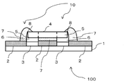
- FIG. 1 is a partial cross-sectional view illustrating a part of an electronic circuit board according to an embodiment of the present invention.
- the electron micrograph showing the cross section in which the void generate
- X-ray transmission is performed through a general chip component mounting board to show “a region under the electrode of the chip component” and “a region where a fillet is formed” for observing whether or not voids are generated. Photo taken from the chip component side using the device.
- the graph showing the area ratio of the void measured in the Example and comparative example of this invention.
- the lead-free solder alloy of this embodiment can contain 1 mass% or more and 3.1 mass% or less of Ag. By adding Ag within this range, an Ag 3 Sn compound can be precipitated in the Sn grain boundary of the lead-free solder alloy, and mechanical strength can be imparted. However, when the Ag content is less than 1% by mass, precipitation of the Ag 3 Sn compound is small, and the mechanical strength and thermal shock resistance of the lead-free solder alloy are lowered, which is not preferable. Moreover, even if Ag is added in an amount exceeding 3.1% by mass, the tensile strength is not significantly improved, and it does not lead to a dramatic improvement in thermal fatigue resistance. It is economically undesirable to increase the content of expensive Ag.
- the Ag content exceeds 4% by mass, the stretchability of the lead-free solder alloy is hindered, and a solder joint formed using this may cause an electrode peeling phenomenon of an electronic component, which is not preferable. Further, when the Ag content is 2% by mass or more and 3.1% by mass or less, the balance between strength and stretchability of the lead-free solder alloy can be improved. A more preferable Ag content is 2.5% by mass or more and 3.1% by mass or less.
- the lead-free solder alloy of this embodiment can contain more than 0 mass% and 1 mass% or less of Cu.
- Cu By adding Cu in this range, the effect of preventing Cu erosion to Cu lands of electronic circuits is exhibited, and the thermal shock resistance of the lead-free solder alloy is improved by precipitating Cu 6 Sn 5 compounds in Sn grain boundaries. Can be improved.
- the Cu content is 0.5 mass% or more and 1 mass% or less, a good Cu erosion prevention effect can be exhibited. In particular, when the Cu content is 0.7% by mass or less, the Cu erosion preventing effect on the Cu land can be exhibited, and the viscosity of the lead-free solder alloy at the time of melting can be maintained in a good state.
- a solder joint formed using a lead-free solder alloy containing Sn, Ag and Cu has an intermetallic compound (for example, Ag 3 Sn, Cu 6 Sn 5 or the like) at the interface between Sn particles.
- an intermetallic compound for example, Ag 3 Sn, Cu 6 Sn 5 or the like.
- the balance of the contents of Ag and Cu is such that Ag is not less than 1% by mass and not more than 3.1% by mass, Cu is more than 0% by mass and not more than 1% by mass, and the Ag content is Cu.
- Ag 3 Sn can be easily formed as the intermetallic compound, and the Cu content can exhibit at least relatively good mechanical properties. That is, even if the Cu content is 1% by mass or less, it contributes to the anti-slipping effect of Ag 3 Sn while part of it becomes an intermetallic compound, so it is good in both Ag 3 Sn and Cu. It is thought that it can exhibit a good mechanical property.
- the lead-free solder alloy of this embodiment can contain 1% by mass to 5% by mass of Sb. By adding Sb within this range, it is possible to improve the crack growth suppressing effect of the solder joint without inhibiting the stretchability of the Sn—Ag—Cu based solder alloy. In addition, in order to improve the said crack progress inhibitory effect, it is preferable that content of Sb shall be 2 mass% or more and 4 mass% or less.
- the lead-free solder alloy in order to withstand the external stress of being exposed to a harsh environment for long periods of time, the lead-free solder alloy has improved toughness (size of the area surrounded by the stress-strain curve) and stretched. It is considered effective to enhance the solid solution by adding an element which dissolves in the Sn matrix and dissolves in the Sn matrix. Then, Sb is an optimum element for solid solution strengthening of the lead-free solder alloy while ensuring sufficient toughness and stretchability.
- fine SnSb and ⁇ -Ag 3 (Sn, Sb) compounds are precipitated at the Sn grain boundaries, thereby preventing the deformation of cracks occurring in the solder joints by preventing slip deformation of the Sn grain boundaries. obtain.
- the solid solution of Sb in the Sn matrix is in a high temperature state, and SnSb, ⁇ -Ag 3 (Sn, Sb) in a low temperature state. Since precipitation of compounds occurs, even when exposed to harsh environments where there is a great difference in temperature, the process of solid solution strengthening at high temperatures and precipitation strengthening at low temperatures is repeated, resulting in excellent cold resistance. It is thought that impact properties can be secured.
- the lead-free solder alloy with Sb added in the above range can improve the strength without reducing the stretchability compared to the Sn-3Ag-0.5Cu solder alloy. Can be secured, and the residual stress can be reduced.
- the stress generated repeatedly is likely to accumulate on the electronic component side of the solder joint. Therefore, deep cracks often occur at solder joints near the electrodes of electronic components. As a result, a stress may be concentrated on the electrode of the electronic component near the crack, and a phenomenon may occur in which the solder joint peels off the electrode on the electronic component side.
- the solder alloy of this embodiment contains Sb within the above range, even if an element that affects the extensibility of the solder alloy such as Bi is contained, the extensibility of the solder alloy is hardly hindered. Even when exposed to a harsh environment for a long time, the electrode peeling phenomenon of electronic components can be suppressed.
- the melting temperature (solidus temperature / liquidus temperature) of the lead-free solder alloy increases, and Sb does not re-dissolve at high temperatures. For this reason, when exposed to a harsh environment where the difference between temperature and temperature is severe, only precipitation strengthening by the SnSb, ⁇ -Ag 3 (Sn, Sb) compound is performed, so that these intermetallic compounds become coarse over time. And the effect of suppressing slip deformation at the Sn grain boundary is lost. Further, in this case, the heat resistance temperature of the electronic component becomes a problem due to an increase in the melting temperature of the lead-free solder alloy, which is not preferable.
- the lead-free solder alloy of this embodiment can contain 0.5 mass% or more and 4.5 mass% or less of Bi. If it is the structure of the lead-free solder alloy of this embodiment, by adding Bi within this range, the strength of the lead-free solder alloy will be improved without affecting the stretchability of the lead-free solder alloy and increased by the addition of Sb.
- the melting temperature can be lowered. That is, since Bi also dissolves into the Sn matrix in the same manner as Sb, the lead-free solder alloy can be further strengthened. However, if the Bi content exceeds 4.5% by mass, the extensibility of the lead-free solder alloy is lowered and the brittleness is increased.
- Bi when the Bi is exposed to a harsh environment where the temperature difference is severe, It is not preferable because a deep crack is likely to occur in a solder joint formed by a free solder alloy.
- the Bi content is 2% by mass or more and 4.5% by mass or less, the strength of the solder joint can be further improved.
- preferable content of Bi is 3.1 mass% or more and 4.5 mass% or less.
- the lead-free solder alloy of this embodiment can contain 0.01 mass% or more and 0.25 mass% or less of Ni. If it is the structure of the lead-free solder alloy of this embodiment, by adding Ni in this range, fine (Cu, Ni) 6 Sn 5 is formed in the molten lead-free solder alloy, and in the base material Since it disperse
- the lead-free solder alloy of the present embodiment allows Ni to move to the vicinity of the interface at the time of soldering even when soldering an electronic component that is not subjected to Ni / Pd / Au plating or Ni / Au plating. Since the fine (Cu, Ni) 6 Sn 5 is formed, the growth of the Cu 3 Sn layer in the vicinity of the interface can be suppressed, and the crack growth suppressing effect in the vicinity of the interface can be improved.
- the content of Ni is less than 0.01% by mass, the effect of modifying the intermetallic compound becomes insufficient, so that the crack suppressing effect near the interface is not sufficiently obtained.
- the Ni content exceeds 0.25% by mass, it is difficult for supercooling to occur as compared with the conventional Sn-3Ag-0.5Cu alloy, and the timing at which the solder alloy solidifies becomes earlier. Therefore, in the fillet of the solder joint portion to be formed, the gas that tried to escape to the outside during melting of the solder alloy is solidified while remaining in it, and a hole (void) due to the gas is generated in the fillet. The case that ends up is confirmed.
- the solder joints should be used especially in environments with a high temperature difference between -40 ° C to 140 ° C and -40 ° C to 150 ° C.
- the thermal fatigue characteristics of the steel will be reduced, and cracks due to voids are likely to occur.
- Ni is likely to generate voids in the fillet.
- Ni is reduced to a value of 0.1 from the balance of the content of Ni and other elements. Even if it is contained in an amount of 25% by mass or less, the generation of the voids can be suppressed.
- Ni content is 0.01% by mass or more and 0.15% by mass or less, it is possible to improve the suppression of void generation while improving the crack growth suppressing effect and heat fatigue resistance near the interface.
- the lead-free solder alloy of this embodiment can contain 0.001% by mass or more and 0.25% by mass or less Co in addition to Ni. If it is the structure of the lead-free solder alloy of this embodiment, by adding Co in this range, the above-mentioned effect by addition of Ni is enhanced and fine (Cu, Co) 6 Sn 5 is contained in the molten lead-free solder alloy. Is formed and dispersed in the base metal, it is possible to improve the thermal fatigue resistance of the solder joints, especially in environments with severe temperature differences, while suppressing creep deformation and crack growth in the solder joints. it can.
- the lead-free solder alloy of the present embodiment enhances the above-described effect due to the addition of Ni even when soldering an electronic component that is not subjected to Ni / Pd / Au plating or Ni / Au plating. Since it moves to the vicinity of the interface during solder bonding to form fine (Cu, Co) 6 Sn 5 , it is possible to suppress the growth of the Cu 3 Sn layer in the vicinity of the interface and to suppress the crack propagation in the vicinity of the interface. Can be improved.
- the Co content is less than 0.001% by mass, the effect of modifying the intermetallic compound becomes insufficient, and therefore, it is difficult to sufficiently obtain the crack suppressing effect near the interface.
- the Co content exceeds 0.25% by mass, overcooling is less likely to occur compared to the conventional Sn-3Ag-0.5Cu alloy, and the timing at which the solder alloy solidifies becomes earlier. Therefore, in the fillet of the solder joint portion to be formed, there is a case in which the gas that tried to escape outside during melting of the solder alloy is solidified while remaining in it, and a void due to the gas is generated in the fillet. It is confirmed.
- the solder joints should be used especially in environments with a high temperature difference between -40 ° C to 140 ° C and -40 ° C to 150 ° C.
- the thermal fatigue characteristics of the steel will be reduced, and cracks due to voids are likely to occur.
- Co easily generates voids in the fillet.
- Co is reduced to 0. 0 from the balance of the contents of Co and other elements. Even if it is contained in an amount of 25% by mass or less, the generation of the voids can be suppressed.
- the Co content is 0.001% by mass or more and 0.15% by mass or less, it is possible to improve the suppression of void generation while improving the good crack growth suppressing effect and the heat fatigue resistance.
- the contents (mass%) of Ag, Cu, Sb, Bi, Ni and Co are expressed by the following formulas (A) to (D). It is preferable to satisfy all of the above.
- the lead-free solder alloy of this embodiment can contain more than 0 mass% and 6 mass% or less In.
- In it is possible to lower the melting temperature of the lead-free solder alloy that has been raised by the addition of Sb and to improve the crack growth suppressing effect. That is, since In dissolves in the Sn matrix as well as Sb, not only can the lead-free solder alloy be further strengthened, but AgSnIn and InSb compounds are formed and precipitated at the Sn grain boundaries. It has the effect of suppressing slip deformation at grain boundaries.
- a more preferable content of In is more than 0% by mass and 4% by mass or less, and particularly preferably 1% by mass or more and 2% by mass or less.
- the lead-free solder alloy of this embodiment can contain 0.001% by mass or more and 0.05% by mass or less of at least one of P, Ga and Ge.
- the lead-free solder alloy of this embodiment can contain 0.001% by mass or more and 0.05% by mass or less of at least one of P, Ga and Ge.
- the lead-free solder alloy of this embodiment can contain at least one of Fe, Mn, Cr, and Mo in a total amount of 0.001% by mass to 0.05% by mass.
- the effect of suppressing crack growth of the lead-free solder alloy can be improved.
- the total amount of these exceeds 0.05% by mass, the melting temperature of the lead-free solder alloy rises, or voids are likely to occur in the soldered joint, which is not preferable.
- the lead-free solder alloy of this embodiment contains other components (elements) such as Cd, Tl, Se, Au, Ti, Si, Al, Mg, Zn, and the like as long as the effect is not hindered. be able to.
- the lead-free solder alloy of this embodiment naturally includes unavoidable impurities.
- the remainder of the lead-free solder alloy of this embodiment is made of Sn.
- preferable Sn content is 79.8 mass% or more and less than 97.49 mass%.
- any method may be used as long as it can form the solder joint portion, such as a flow method, mounting with a solder ball, and a reflow method using a solder paste composition. .
- a reflow method using a solder paste composition is particularly preferred.
- solder paste composition of the present embodiment includes, for example, a powdered lead-free solder alloy, (A) a base resin, (B) an activator, (C) a thixotropic agent, D) It is produced by kneading a flux composition containing a solvent into a paste.
- the base resin (A) for example, at least one of (A-1) rosin resin and (A-2) synthetic resin is preferably used.
- Examples of the rosin resin (A-1) include rosins such as tall oil rosin, gum rosin, and wood rosin; polymerization, hydrogenation, heterogeneity, acrylation, maleation, esterification, or phenol addition reaction of rosin. And a modified rosin resin obtained by subjecting these rosin or rosin derivative and an unsaturated carboxylic acid (acrylic acid, methacrylic acid, maleic anhydride, fumaric acid, etc.) to a Diels-Alder reaction.
- a modified rosin resin is particularly preferably used, and a hydrogenated acrylic acid-modified rosin resin hydrogenated by reacting acrylic acid is particularly preferably used.
- the acid value of the rosin resin (A-1) is preferably 140 mgKOH / g to 350 mgKOH / g, and its mass average molecular weight is preferably 200 Mw to 1,000 Mw.
- Examples of the synthetic resin (A-2) include acrylic resins, styrene-maleic resins, epoxy resins, urethane resins, polyester resins, phenoxy resins, terpene resins, polyalkylene carbonates, rosin resins having carboxyl groups, and dimer acids.
- Derivative compounds formed by dehydration condensation with a derivative flexible alcohol compound are exemplified. In addition, you may use these individually by 1 type or in mixture of multiple types.
- an acrylic resin is particularly preferably used.
- the acrylic resin can be obtained by, for example, homopolymerizing (meth) acrylate having an alkyl group having 1 to 20 carbon atoms or copolymerizing a monomer having the acrylate as a main component.
- acrylic resins obtained by polymerizing methacrylic acid and monomers containing two saturated alkyl groups having 2 to 20 carbon atoms in which the carbon chain is linear are preferably used. It is done. In addition, you may use the said acrylic resin individually by 1 type or in mixture of multiple types.
- rosin derivative compound obtained by dehydrating and condensing the rosin resin having a carboxyl group and a dimer acid derivative flexible alcohol compound
- Rosin resin having a carboxyl group for example, Rosin such as tall oil rosin, gum rosin, wood rosin; hydrogenated rosin, polymerized rosin, heterogeneous rosin, acrylic acid modified rosin, rosin derivatives such as maleic acid modified rosin, etc. Can be used. These may be used alone or in combination of two or more.
- examples of the dimer acid derivative flexible alcohol compound include compounds derived from dimer acid such as dimer diol, polyester polyol, and polyester dimer diol, and those having an alcohol group at the terminal thereof.
- dimer acid such as dimer diol, polyester polyol, and polyester dimer diol
- PRIPOL 2033, PRIPLAST 3197, PRIPLAST 1838 (manufactured by Croda Japan Co., Ltd.) and the like can be used.
- the rosin derivative compound is obtained by dehydrating and condensing the rosin resin having a carboxyl group and the dimer acid derivative flexible alcohol compound.
- the dehydration condensation method a generally used method can be used.
- a preferable mass ratio when dehydrating and condensing the rosin resin having a carboxyl group and the dimer acid derivative flexible alcohol compound is 25:75 to 75:25, respectively.
- the acid value of the synthetic resin (A-2) is preferably 10 mgKOH / g to 150 mgKOH / g, and its mass average molecular weight is preferably 1,000 Mw to 30,000 Mw.
- the blending amount of the base resin (A) is preferably 10% by mass or more and 60% by mass or less, and more preferably 30% by mass or more and 55% by mass or less with respect to the total amount of the flux composition.
- the acid value of the base resin (A) is preferably 10 mgKOH / g or more and 250 mgKOH / g or less, and its mass average molecular weight is preferably 300 Mw to 30,000 Mw.
- the blending amount thereof is preferably 20% by mass or more and 60% by mass or less, and preferably 30% by mass or more and 55% by mass or less with respect to the total amount of the flux composition. More preferably.
- the blending amount is preferably 10% by mass or more and 60% by mass or less, and more preferably 15% by mass or more and 50% by mass or less with respect to the total amount of the flux composition. It is more preferable.
- the blending ratio is preferably 20:80 to 50:50, and 25:75 to 40:60. More preferably.
- the base resin (A) is preferably a rosin resin (A-1) alone or a combination of acrylic resin as the rosin resin (A-1) and the synthetic resin (A-2).
- activator (B) examples include amine salts (inorganic acid salts and organic acid salts) such as hydrogen halide salts of organic amines, organic acids, organic acid salts, organic amine salts, and the like. .
- amine salts organic acid salts and organic acid salts
- diphenylguanidine hydrobromide, cyclohexylamine hydrobromide, diethylamine salt, dimer acid, levulinic acid, lactic acid, acrylic acid, benzoic acid, salicylic acid, anisic acid, citric acid, 1,4- Examples include cyclohexanedicarboxylic acid, anthranilic acid, picolinic acid and 3-hydroxy-2-naphthoic acid.
- the blending amount of the activator (B) is preferably 4.5% by mass or more and 35% by mass or less with respect to the total amount of the flux composition.
- the active agents (B) including the active agents listed in the following active agents (B-1), (B-2) and (B-3) may be used singly or in combination. Good.
- (B-1) a linear saturated dicarboxylic acid having 3 to 4 carbon atoms is added to the flux composition as the activator (B) with respect to the total amount of the flux composition.
- (B-3) carbon number 20 to 22 dicarboxylic acid is preferably blended in an amount of 2% by mass or more and 15% by mass or less based on the total amount of the flux composition.
- the total amount of these active agents (B-1), (B-2) and (B-3) is preferably 4.5% by mass or more and 35% by mass or less, and more preferably 4.5% by mass or more. More preferably, it is 20 mass% or less.
- the linear saturated dicarboxylic acid (B-1) having 3 to 4 carbon atoms is preferably at least one of malonic acid and succinic acid.
- a more preferable blending amount of the linear saturated dicarboxylic acid (B-1) having 3 to 4 carbon atoms is 0.5% by mass to 2% by mass with respect to the total amount of the flux composition.
- the carbon chain in the dicarboxylic acid (B-2) having 5 to 13 carbon atoms may be either linear or branched, but glutaric acid, adipic acid, pimelic acid, suberic acid, azelaic acid 2-methyl azelaic acid, sebacic acid, undecanedioic acid, 2,4-dimethyl-4-methoxycarbonylundecanedioic acid, dodecanedioic acid, tridecanedioic acid, and 2,4,6-trimethyl-4,6-dimethoxy It is preferably at least one selected from carbonyl tridecanedioic acid.
- adipic acid, suberic acid, sebacic acid and dodecanedioic acid are particularly preferably used.
- a more preferable amount of the dicarboxylic acid (B-2) having 5 to 13 carbon atoms is 3% by mass to 12% by mass with respect to the total amount of the flux composition.
- the carbon chain may be either linear or branched, but eicosadioic acid, 8-ethyloctadecanedioic acid, 8,13 It is preferably at least one selected from -dimethyl-8,12-eicosadiene diacid and 11-vinyl-8-octadecenedioic acid.
- the dicarboxylic acid (B-3) having 20 to 22 carbon atoms those that are liquid or semi-solid at room temperature are more preferably used.
- normal temperature refers to a range of 5 ° C to 35 ° C.
- the semi-solid state refers to a state corresponding to a state between a liquid state and a solid state, a part of which has fluidity and a state of non-fluidity but deformed when external force is applied.
- 8-ethyloctadecanedioic acid is particularly preferably used.
- a more preferable amount of the dicarboxylic acid (B-3) having 20 to 22 carbon atoms is 3% by mass to 12% by mass with respect to the total amount of the flux composition.
- the linear saturated dicarboxylic acid (B-1) having 3 to 4 carbon atoms partially coats the surface of the alloy powder when the flux composition and the alloy powder are kneaded.
- the surface oxidation can be suppressed.
- the dicarboxylic acid (B-3) having 20 to 22 carbon atoms is slow in reactivity, so that it is stable in the printing process of the solder paste composition on the substrate for a long time and also volatilizes during reflow heating. Since it is difficult to do so, the surface of the molten alloy powder can be covered and oxidation can be suppressed by a reducing action.
- the dicarboxylic acid (B-3) having 20 to 22 carbon atoms has low activity, and the oxide film on the surface of the alloy powder can be obtained only in combination with the linear saturated dicarboxylic acid (B-1) having 3 to 4 carbon atoms. May not be sufficiently removed. Therefore, especially when an alloy powder made of the lead-free solder alloy containing a large amount of Bi, In, Sb, etc. is used, the oxidizing action on the alloy powder tends to be insufficient, and the effect of suppressing solder balls and voids is not sufficiently exhibited. There is a fear.
- the flux composition contains dicarboxylic acid (B-2) having 5 to 13 carbon atoms that exerts a strong activity from preheating within the above range, the reliability of the flux residue is ensured while ensuring the reliability of the flux residue. Even when such an alloy powder is used, the oxide film can be sufficiently removed. Therefore, the solder paste composition of the present embodiment improves the cohesive force between the alloy powders and reduces the viscosity at the time of melting the solder, thereby suppressing solder balls generated on the side of the electronic component or solder joining. The void generated in the part can be further reduced. Moreover, the flux composition combined with such an activator can also exhibit good printability.
- B-2 dicarboxylic acid
- the lead-free solder alloy of the present embodiment can suppress the generation of voids along with the suppression of crack propagation to the formed solder joint due to the balance between the composition and the content of the lead-free solder alloy itself. it can.
- the dicarboxylic acid corresponding to the specific carbon number range of the activator (B-1), (B-2) and (B-3) is used in combination at a predetermined blending amount in the flux composition, It can exhibit a redox effect on a good solder alloy. Therefore, in this case, the surface oxide film of the alloy powder can be more sufficiently removed in the lead-free solder alloy of the present embodiment to which highly oxidizable elements such as Bi, In, and Sb are added.
- solder paste composition can suppress the generation of solder balls due to the difficulty of agglomeration and fusion of alloy powders, and can exhibit good printability.
- thixotropic agent (C) Thixotropic agent
- the thixotropic agent (C) include hydrogenated castor oil, fatty acid amides, saturated fatty acid bisamides, oxy fatty acids, and dibenzylidene sorbitols. You may use these individually by 1 type or in mixture of multiple types.
- the blending amount of the thixotropic agent (C) is preferably 2% by mass or more and 15% by mass or less, and more preferably 2% by mass or more and 10% by mass or less with respect to the total amount of the flux composition.
- solvent (D) Solvent examples include isopropyl alcohol, ethanol, acetone, toluene, xylene, ethyl acetate, ethyl cellosolve, butyl cellosolve, hexyl diglycol, (2-ethylhexyl) diglycol, phenyl glycol, butyl carbitol. , Octanediol, ⁇ -terpineol, ⁇ -terpineol, tetraethylene glycol dimethyl ether, trimellitic acid tris (2-ethylhexyl), bisisopropyl sebacate and the like. You may use these individually by 1 type or in mixture of multiple types.
- the blending amount of the solvent (D) is preferably 20% by mass or more and 50% by mass or less, and more preferably 25% by mass or more and 40% by mass or less with respect to the total amount of the flux composition.
- an antioxidant may be blended for the purpose of suppressing oxidation of the alloy powder.
- the antioxidant include hindered phenolic antioxidants, phenolic antioxidants, bisphenolic antioxidants, and polymer-type antioxidants. Of these, hindered phenol-based oxidizing agents are particularly preferably used. You may use these individually by 1 type or in mixture of multiple types.
- the blending amount of the antioxidant is not particularly limited, but generally it is preferably about 0.5% by mass or more and about 5% by mass or less based on the total amount of the flux composition.
- An additive can be blended with the flux composition as necessary.
- the additive include an antifoaming agent, a surfactant, a matting agent, and an inorganic filler. You may use these individually or in mixture of multiple types.
- the blending amount of the additive is preferably 0.5% by mass or more and 20% by mass or less, and more preferably 1% by mass or more and 15% by mass or less with respect to the total amount of the flux composition.
- the mixing ratio of the lead-free solder alloy powder and the flux composition is preferably 65:35 to 95: 5 in the ratio of solder alloy powder: flux.
- a more preferred blending ratio is 85:15 to 93: 7, and a particularly preferred blending ratio is 87:13 to 92: 8.
- the average particle size of the alloy powder is preferably 1 ⁇ m or more and 40 ⁇ m or less, more preferably 5 ⁇ m or more and 35 ⁇ m or less, and particularly preferably 10 ⁇ m or more and 30 ⁇ m or less.
- the electronic circuit board 100 of this embodiment includes a substrate 1, an insulating layer 2, an electrode part 3, an electronic component 4, and a solder joint body 10.
- the solder joint body 10 has a solder joint portion 6 and a flux residue 7, and the electronic component 4 has an external electrode 5 and an end portion 8.
- the substrate 1 can be used as the substrate 1 as long as it is used for mounting and mounting electronic components such as a printed wiring board, a silicon wafer, and a ceramic package substrate.
- the electrode portion 3 is electrically joined to the external electrode 5 of the electronic component 4 via the solder joint portion 6.
- the solder joint 6 is formed using the lead-free solder alloy according to the present embodiment.
- the electronic circuit board 100 according to the present embodiment having such a configuration has an alloy composition in which the solder joint portion 6 exhibits an effect of suppressing crack propagation, the crack is generated even when the solder joint portion 6 is cracked. Can suppress the progress of In particular, even when the electronic component 4 is not subjected to Ni / Pd / Au plating or Ni / Au plating, the effect of suppressing crack propagation near the interface between the solder joint 6 and the electronic component 4 can also be exhibited. . Thereby, the electrode peeling phenomenon of the electronic component 4 can also be suppressed. Moreover, since the solder joint part 6 uses the lead-free solder alloy of this embodiment, generation
- Such an electronic circuit board 100 is manufactured as follows, for example. First, the solder paste composition is printed according to the above pattern on a substrate 1 provided with an insulating layer 2 and an electrode portion 3 formed to have a predetermined pattern. Next, the electronic component 4 is mounted on the printed board 1 and reflowed at a temperature of 230 ° C. to 260 ° C. By this reflow, the solder joint 10 having the solder joint 6 and the flux residue 7 is formed on the substrate 1, and the electronic circuit board 100 in which the substrate 1 and the electronic component 4 are electrically joined is manufactured.
- the solder joined body 10 contains a dicarboxylic acid corresponding to a specific carbon number range of the activators (B-1), (B-2) and (B-3) in the flux composition at a predetermined blending amount.
- the surface oxide film of the alloy powder of the lead-free solder alloy of this embodiment can be more sufficiently removed. Therefore, it is possible to further suppress the remaining of voids in the solder joint and further suppress the crack progress of the solder joint. Further, since such a solder paste composition makes it difficult for the alloy powders to agglomerate and fuse together, it is possible to suppress the generation of solder balls on the substrate 1 and to provide an electronic circuit substrate 100 having higher reliability. be able to.
- the electronic control device of the present embodiment is manufactured.
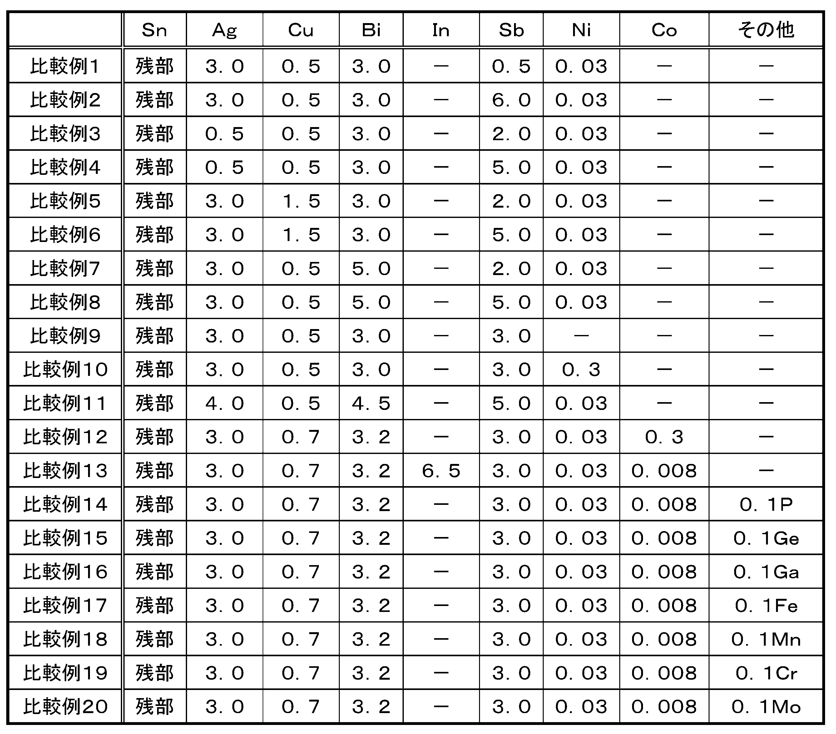
- solder Paste Composition 11.0% by mass of the flux composition was mixed with 89.0% by mass of each lead-free solder alloy powder (powder particle size 20 ⁇ m to 38 ⁇ m) listed in Tables 1 and 2.
- each solder paste composition according to Examples 1 to 33 and Comparative Examples 1 to 20 was prepared.
- solder crack test (-40 ° C to 125 ° C) ⁇ 3.2mm ⁇ 1.6mm chip parts (chip A)
- a chip component Ni / Sn plating having a size of 3.2 mm ⁇ 1.6 mm, a solder resist having a pattern capable of mounting the chip component of the size, and an electrode (1.6 mm ⁇ 1.2 mm) connecting the chip component And a 150 ⁇ m-thick metal mask having the same pattern were prepared.
- Each solder paste composition was printed on the glass epoxy substrate using the metal mask, and the chip component was mounted on each of the solder paste compositions.
- each glass epoxy substrate is heated to solder the glass epoxy substrate and the chip component to each other electrically. A part was formed, and the chip component was mounted.
- the reflow conditions at this time are: preheating from 170 ° C. to 190 ° C. for 110 seconds, peak temperature of 245 ° C., time of 200 ° C. or higher for 65 seconds, time of 220 ° C. or higher for 45 seconds, peak temperature to 200 ° C.
- the cooling rate was 3 ° C. to 8 ° C./second, and the oxygen concentration was set to 1500 ⁇ 500 ppm.
- chip B A chip component (Ni / Sn plating) having a size of 2.0 mm ⁇ 1.2 mm, a solder resist having a pattern capable of mounting the chip component of the size, and an electrode (1.25 mm ⁇ 1.0 mm) for connecting the chip component A test substrate was prepared under the same conditions as those of a 3.2 mm ⁇ 1.6 mm chip component except that a glass epoxy substrate provided with the above was used, and evaluated by the same method. The results are shown in Table 3 and Table 4.
- the glass epoxy board was subjected to a thermal shock under the same conditions as in the solder crack test (1) except that each glass epoxy board was placed in an environment where the thermal shock cycle was repeated 1,000, 2,000, and 3,000 cycles.
- Each test substrate was prepared. Subsequently, the target part of each test board
- solder base material in this specification, the solder base material refers to the portion other than the interface of the electrode of the SON component and the vicinity thereof in the solder joint portion.
- base metal in Table 4, it is simply described as “base metal”.
- Evaluation was performed as follows by dividing into cracks occurring at the interface between the solder joint and the electrode of the SON component (intermetallic compound). . The results are shown in Table 3 and Table 4. Note that the number of SONs evaluated in each thermal shock cycle was 20, and one terminal of the gate electrode was observed per SON, and the cross section of a total of 20 terminals was confirmed.
- a crack that occurred at the interface between the solder joint and the electrode of the SON part ⁇ No crack that completely traverses the interface until 3,000 cycles ⁇ : The interface was completely completed between 2,001 to 3,000 cycles ⁇ : A crack that completely crosses the interface between 1,001 and 2,000 cycles is generated. ⁇ : A crack that completely crosses the interface is generated in 1,000 cycles or less.
- solder crack test (-40 ° C to 150 ° C) Since in-vehicle boards and the like are placed in a severe environment where the temperature difference is extremely severe, it is required that the solder alloy used therein exhibits a good crack growth suppressing effect even in such an environment. Therefore, in order to clarify whether the solder alloy according to the present embodiment can exhibit the effect even under such severe conditions, it is ⁇ 40 ° C. to 150 ° C. using a liquid tank type thermal shock test apparatus. The solder crack test in the temperature difference of was conducted. The conditions are as follows.
- a liquid bath type thermal shock test device (product name: ETAC WINTECH LT80, manufactured by Enomoto Co., Ltd.) in which each glass epoxy board after solder joint formation is set to a condition of ⁇ 40 ° C. (5 minutes) to 150 ° C. (5 minutes) 3.2 mm ⁇ 1.6 mm chip components under the same conditions as the solder crack test (1) except that the thermal shock cycle is exposed to an environment where 1,000, 2,000, and 3,000 cycles are repeated.
- Each test substrate mounted with chip A) and 2.0 mm ⁇ 1.2 mm chip component (chip B) was prepared.
- the number of evaluation chips in each thermal shock cycle was 10.
- the reflow conditions were the same as in the solder crack test (1).
- the surface state of each test substrate was observed with an X-ray transmission device (product name: SMX-160E, manufactured by Shimadzu Corporation), and the area under the electrode of the chip component (see FIG. 3 is the void area ratio (ratio of the total area of voids; the same applies hereinafter) and the area where fillets are formed (area (b) surrounded by broken lines in FIG. 3).
- the average value of the area ratio of voids in each was obtained and evaluated for each as follows. The results are shown in Table 3 and Table 4.
- ⁇ The average value of the void area ratio is more than 3% and 5% or less, and the effect of suppressing the generation of voids.
- ⁇ The average value of the void area ratio is more than 5% and 8% or less, and the effect of suppressing the generation of voids is sufficient.
- ⁇ The average value of the void area ratio exceeds 8%, and the effect of suppressing the generation of voids insufficient
- the solder joint formed by using the lead-free solder alloy according to Examples 1 to 33 can be used even in a severe environment where the difference in temperature is intense and vibration is applied. Regardless of the size, and regardless of whether the electrode is Ni / Pd / Au plated or Ni / Au plated, it is possible to exert an effect of suppressing crack propagation near the solder joint and the interface. In particular, it can be seen that the solder joints of the examples have a good crack suppression effect even in a very severe environment where the difference in temperature is -40 ° C. to 150 ° C. using a liquid tank type thermal shock test apparatus.
- Examples 16 to 33 using Ni and Co in combination a good solder joint and crack growth suppressing effect near the interface can be exhibited under any conditions. Further, in this example, even when Bi, Sb, Ni, Co or the like having high oxidizability is contained in a certain amount or more, the crack growth suppressing effect is improved while exhibiting a favorable void suppressing effect. Can do. In addition, even if it is a case where 0.25 mass% of Ni or Co is contained as in Example 17 or Example 22, for example, generation of voids in the fillet can be suppressed.
- the lead-free solder alloy according to Example 15 contains 4.5% by mass of highly oxidative Bi and 5% by mass of Sb, combinations with other alloy elements and these It turns out that a favorable void inhibitory effect can be exhibited with a crack growth inhibitory effect by content balance.
- the lead-free solder alloy according to Comparative Example 11 containing 4.5% by mass of Bi and 5% by mass of Sb and containing 4% by mass of Ag, the void of the fillet is obtained as a result of the void test (4). Is ⁇ . Therefore, an electronic circuit board having such a solder joint can be suitably used for an electronic circuit board that has a severe temperature difference and requires high reliability, such as an in-vehicle electronic circuit board. Furthermore, such an electronic circuit board can be suitably used for an electronic control device that requires higher reliability.
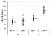
- solder paste compositions Example 34 and Comparative Example 21.
- Solder Alloy Powder Example 34 Sn-3.1Ag-0.7Cu-3.2Bi-3Sb-0.03Ni
- Comparative Example 21 Sn-3.4Ag-0.7Cu-3.2Bi-3Sb-0.03Ni
- FIG. 4 shows a graph of the following results.
- the lead-free solder alloy of this example contains a predetermined alloy element within a predetermined range, so that in any of the region under the chip component electrode and the region where the fillet is formed. It can be clearly seen that the generation of voids can be suppressed.
- dimethyl 2,2′-azobis (2-methylpropionate) product name: V-601, manufactured by Wako Pure Chemical Industries, Ltd.
- V-601 dimethyl 2,2′-azobis (2-methylpropionate)
- mass% was added to dissolve it.
- This solution was added dropwise to the four-necked flask over 1.5 hours, and the components in the four-necked flask were stirred at 110 ° C. for 1 hour, and then the reaction was terminated to obtain a synthetic resin.
- the weight average molecular weight of the synthetic resin was 7,800 Mw, the acid value was 40 mgKOH / g, and the glass transition temperature was ⁇ 47 ° C.
- each component described in Table 6 and Table 7 was kneaded to obtain each flux composition according to Examples 35 to 46 and Comparative Examples 22 to 35.
- the unit of the compounding amount in Tables 6 and 7 is mass%.
- solder paste composition according to Examples 35 to 46 and Comparative Examples 22 to 35 was prepared by kneading 11.2% by mass of the flux composition and 88.8% by mass of the following solder alloy powder. A product was made.
- the number of balls generated around 10 chip resistors of 2.0 mm ⁇ 1.2 mm exceeds 0 and less than 5.
- the number of balls generated around 10 chip resistors of 2.0 mm ⁇ 1.2 mm exceeds 5 and less than 10
- the number of balls generated around 10 chip resistors of 2.0 mm ⁇ 1.2 mm exceeds 10
- solder crack test A chip component having a size of 3.2 mm ⁇ 1.6 mm, a solder resist having a pattern capable of mounting the chip component of the size, and an electrode for connecting the chip component (1.6 mm ⁇ 1.2 mm) And a 150 ⁇ m-thick metal mask having the same pattern were prepared.
- Each solder paste composition was printed on the glass epoxy substrate using the metal mask, the chip components were mounted on each glass paste substrate, and solder joints were formed.
- the reflow conditions at this time are: preheating from 170 ° C. to 190 ° C. for 110 seconds, peak temperature of 245 ° C., time of 200 ° C. or higher for 65 seconds, time of 220 ° C.
- a liquid bath type thermal shock test apparatus (product name: ETAC WINTECH LT80, Enomoto Co., Ltd.) in which each glass epoxy substrate after the formation of the solder joint is set to a temperature of -40 ° C. (5 minutes) to 150 ° C. (5 minutes). Each test substrate was manufactured by exposing the thermal shock cycle to an environment where 1,000, 2,000, and 3,000 cycles were repeated.
- the number of evaluation chips in each thermal shock cycle was 10.
- solder paste compositions of Examples 35 to 46 are combined with a lead-free solder alloy capable of suppressing the generation of voids in the formed solder joints and exhibiting a good crack growth suppressing effect, and the activator in the flux composition.
- Dicarboxylic acids corresponding to specific carbon number ranges of (B-1), (B-2) and (B-3) are used in combination at a predetermined blending amount. Therefore, it is possible to exert a good redox action on the solder alloy, and the surface oxide film of the lead-free solder alloy powder can be more sufficiently removed. Therefore, it is possible to further suppress the residual of voids in the solder joints even in a severe environment where the difference in temperature is severe and the vibration is applied, especially in the severe temperature difference of ⁇ 40 ° C.
- solder paste composition can suppress generation
- the lead-free solder alloy and the solder paste composition of the present invention can be suitably used for an electronic circuit board that is required to have high reliability such as an in-vehicle electronic circuit board. Furthermore, such an electronic circuit board can be suitably used for an electronic control device that requires higher reliability.
Landscapes
- Engineering & Computer Science (AREA)
- Mechanical Engineering (AREA)
- Chemical & Material Sciences (AREA)
- Materials Engineering (AREA)
- Metallurgy (AREA)
- Organic Chemistry (AREA)
- Microelectronics & Electronic Packaging (AREA)
- Manufacturing & Machinery (AREA)
- Dispersion Chemistry (AREA)
- Electric Connection Of Electric Components To Printed Circuits (AREA)
Abstract
Description
鉛フリーはんだ合金は、鉛含有はんだ合金と比較してはんだ付性が多少劣るものの、フラックスやはんだ付装置の改良によってこのはんだ付性の問題はカバーされている。そのため、例えば車載用電子回路基板であっても、自動車の車室内のように寒暖差はあるものの比較的穏やかな環境下に置かれるものにおいては、Sn-3Ag-0.5Cuはんだ合金を用いて形成したはんだ接合部でも大きな問題は生じていない。
そのため、上述の過酷な環境下に置かれる車載用電子回路基板および電子制御装置が増える中で、十分な亀裂進展抑制効果を発揮し得るSn-Ag-Cu系はんだ合金やこれを用いたソルダペースト組成物への要望は、今後ますます大きくなることが予想される。
はんだ接合時において、Snめっきされた電子部品は、Snめっきおよびはんだ接合部に含まれるSnとリード部分や前記下面電極に含まれるCuとの相互拡散を発生させ易い。この相互拡散により、はんだ接合部と前記リード部分や前記下面電極との界面付近の領域(以下、本明細書においては「界面付近」という。)にて、金属間化合物であるCu3Sn層が凸凹状に大きく成長する。前記Cu3Sn層は元々硬くて脆い性質を有する上に、凸凹状に大きく成長したCu3Sn層は更に脆くなる。そのため、特に上述の過酷な環境下においては、前記界面付近ははんだ接合部と比較して亀裂が発生し易く、また発生した亀裂はこれを起点として一気に進展するため、電気的短絡が生じ易い。
従って、今後は上述の過酷な環境下でNi/Pd/AuめっきやNi/Auめっきがなされていない電子部品を用いた場合であっても前記界面付近における亀裂進展抑制効果を発揮し得る鉛フリーはんだ合金への要望も大きくなることが予想される。
特にSn-Ag-Cu系はんだ合金にBiやInおよびSbといった酸化性の高い元素を添加する場合、Sn-3Ag-0.5Cu系はんだ合金よりもその合金粉末の表面酸化膜を十分に除去し難い傾向にある。そのため特にソルダペースト組成物においては、使用するフラックス組成物の活性力が不十分であると、溶融した合金粉末の粘性が下がり難くなりはんだ接合部にボイドが残留し易く、合金粉末同士が凝集・融合し難くなりはんだボールが発生し易くなる。はんだボールは基板上に実装された電子部品の電極とソルダペースト組成物との未融合現象といったオープン不良やショートの原因となるため、特に高信頼性が要求される車載用電子回路基板においては、はんだボールの発生の抑制は重要な課題の一つである。
また例えばはんだ接合部のうち前記界面付近にボイドが発生すると、電子部品が左右対称ではない状態で(基板上の電極上部且つ電子部品の下面電極の下部に位置するはんだ接合部の厚みが均一ではない状態で)基板に接合され易くなる。このため、はんだ接合部のうち、その厚みのない(薄い)部分の接合寿命は一層短くなってしまう。そしてこのようなはんだ接合部は、特に寒暖の差の激しい環境においてはその厚みのない部分から亀裂が入り易く、またその亀裂進展も起き易くなる。
更には、はんだ接合部のうちフィレット部にボイドが発生すると、フィレット部にボイドのないはんだ接合部と比較してボイドの体積分、亀裂経路が短くなるため、はんだ接合部を横断する亀裂が起き易くなる虞がある。
1.6≦Ag含有量+(Cu含有量/0.5)≦5.9 … A
0.85≦(Ag含有量/3)+(Bi含有量/4.5)≦ 2.10 … B
3.6 ≦ Ag含有量+Sb含有量≦ 8.9 … C
0<(Ni含有量/0.25)+(Co含有量/0.25)≦1.19 …D
本実施形態の鉛フリーはんだ合金には、1質量%以上3.1質量%以下のAgを含有させることができる。この範囲内でAgを添加することにより、鉛フリーはんだ合金のSn粒界中にAg3Sn化合物を析出させ、機械的強度を付与することができる。
但し、Agの含有量が1質量%未満の場合、Ag3Sn化合物の析出が少なく、鉛フリーはんだ合金の機械的強度および耐熱衝撃性が低下するので好ましくない。またAgを3.1質量%を超えて添加しても引っ張り強度は大幅には向上せず、飛躍的な耐熱疲労特性の向上には結びつかない。また高価なAgの含有量を増やすことは経済的に好ましくない。更にAgの含有量が4質量%を超える場合、鉛フリーはんだ合金の延伸性が阻害され、これを用いて形成されるはんだ接合部が電子部品の電極剥離現象を引き起こす虞があるので好ましくない。
またAgの含有量を2質量%以上3.1質量%以下とすると、鉛フリーはんだ合金の強度と延伸性のバランスをより良好にできる。更に好ましいAgの含有量は2.5質量%以上3.1質量%以下である。
Cuの含有量を0.5質量%以上1質量%以下とすると良好なCu喰われ防止効果を発揮することができる。特にCuの含有量が0.7質量%以下の場合、Cuランドに対するCu食われ防止効果を発揮することができると共に、溶融時の鉛フリーはんだ合金の粘度を良好な状態に保つことができ、リフロー時におけるボイドの発生をより抑制し、形成するはんだ接合部の耐熱衝撃性を向上することができる。更には、溶融した鉛フリーはんだ合金のSn結晶粒界に微細なCu6Sn5が分散することで、Snの結晶方位の変化を抑制し、はんだ接合形状(フィレット形状)の変形を抑制することができる。
なおCuの含有量が1質量%を超えると、はんだ接合部の電子部品および電子回路基板との界面近傍にCu6Sn5化合物が析出し易くなり、接合信頼性やはんだ接合部の延伸性を阻害する虞があるため好ましくない。
ここで一般的にSn、AgおよびCuを含有する鉛フリーはんだ合金を用いて形成されるはんだ接合部は、Sn粒子同士の界面に金属間化合物(例えばAg3Sn、Cu6Sn5等)が分散し、はんだ接合部に引っ張りの力が加えられた場合であってもSn粒子同士が滑って変形するといった現象を防止し得る構造体となり、これにより所謂機械的特性を発現し得る。即ち、上記金属間化合物がSn粒子の滑り止め的な役割を果たす。
従って前記鉛フリーはんだ合金の場合、AgとCuの含有量のバランスをAgを1質量%以上3.1質量%以下、Cuを0質量%超1質量%以下とし、Agの含有量をCuの含有量よりも同量以上とすることで、上記金属間化合物としてAg3Snが形成され易くなり、Cuの含有量が比較的少なくとも良好な機械的特性を発現し得る。つまり、Cuの含有量が1質量%以下であったとしても、その一部が金属間化合物になりつつもAg3Snの滑り止め効果に寄与することから、Ag3SnとCuの両方において良好な機械的特性を発揮し得ると考えられる。
即ち、実質的に母材(本明細書においては鉛フリーはんだ合金の主要な構成要素を指す。以下同じ。)をSnとする鉛フリーはんだ合金に上記範囲でSbを添加することで、Snの結晶格子の一部がSbに置換され、その結晶格子に歪みが発生する。そのため、このような鉛フリーはんだ合金を用いて形成されるはんだ接合部は、Sn結晶格子の一部のSb置換により前記結晶中の転移に必要なエネルギーが増大してその金属組織が強化される。更には、Sn粒界に微細なSnSb、ε-Ag3(Sn,Sb)化合物が析出することにより、Sn粒界のすべり変形を防止することではんだ接合部に発生する亀裂の進展を抑制し得る。
なるため好ましくない。
またBiの含有量を2質量%以上4.5質量%以下とすると、はんだ接合部の強度をより向上させることができる。また後述するNiおよび/またはCoと併用する場合、Biの好ましい含有量は3.1質量%以上4.5質量%以下である。
また、本実施形態の鉛フリーはんだ合金は、Ni/Pd/AuめっきやNi/Auめっきがなされていない電子部品をはんだ接合する場合であっても、はんだ接合時にNiが前記界面付近に移動して微細な(Cu,Ni)6Sn5を形成するため、その界面付近におけるCu3Sn層の成長を抑制することができ、前記界面付近の亀裂進展抑制効果を向上させることができる。
なお、上述の通りNiはフィレット中にボイドを発生し易いものであるが、本実施形態の鉛フリーはんだ合金の構成においては、Niと他の元素との含有量のバランスから、Niを0.25質量%以下含有させても上記ボイドの発生を抑制することができる。
なお、上述の通りCoはフィレット中にボイドを発生し易いものであるが、本実施形態の鉛フリーはんだ合金の構成においては、Coと他の元素との含有量のバランスから、Coを0.25質量%以下含有させても上記ボイドの発生を抑制することができる。
1.6≦Ag含有量+(Cu含有量/0.5)≦5.9 … A
0.85≦(Ag含有量/3)+(Bi含有量/4.5)≦ 2.10 … B
3.6 ≦ Ag含有量+Sb含有量≦ 8.9 … C
0<(Ni含有量/0.25)+(Co含有量/0.25)≦1.19 …D
AgとCuとSbとBiとNiとCoの含有量を上記範囲内とすることで、はんだ接合部の延伸性阻害および脆性増大の抑制、はんだ接合部の強度および熱疲労特性の向上、フィレット中に発生するボイドの抑制、寒暖の差が激しい過酷な環境下におけるはんだ接合部の亀裂進展抑制、Ni/Pd/AuめっきやNi/Auめっきがなされていない電子部品のはんだ接合時における前記界面付近の亀裂進展抑制効果のいずれもバランスよく発揮させることができ、はんだ接合部の信頼性を一層向上させることができる。
本発明のはんだ合金に添加するInの含有量が6質量%を超えると、鉛フリーはんだ合金の延伸性を阻害すると共に、寒暖の差が激しい過酷な環境下に長時間曝されている間にγ-InSn4が形成され、鉛フリーはんだ合金が自己変形してしまうため好ましくない。
なお、Inのより好ましい含有量は、0質量%超4質量%以下であり、1質量%以上2質量%以下が特に好ましい。
本実施形態のソルダペースト組成物は、例えば粉末状にした前記鉛フリーはんだ合金と(A)ベース樹脂と、(B)活性剤と、(C)チキソ剤と、(D)溶剤とを含むフラックス組成物とを混練しペースト状にすることにより作製される。
前記ベース樹脂(A)としては、例えば(A-1)ロジン系樹脂および(A-2)合成樹脂の少なくとも一方を用いることが好ましい。
次に前記ダイマー酸誘導体柔軟性アルコール化合物としては、例えばダイマージオール、ポリエステルポリオール、ポリエステルダイマージオールのようなダイマー酸から誘導される化合物であって、その末端にアルコール基を有するもの等が挙げられ、例えばPRIPOL2033、PRIPLAST3197、PRIPLAST1838(以上、クローダジャパン(株)製)等を用いることができる。
前記ロジン誘導体化合物は、前記カルボキシル基を有するロジン系樹脂と前記ダイマー酸誘導体柔軟性アルコール化合物とを脱水縮合することにより得られる。この脱水縮合の方法としては一般的に用いられる方法を使用することができる。また、前記カルボキシル基を有するロジン系樹脂と前記ダイマー酸誘導体柔軟性アルコール化合物とを脱水縮合する際の好ましい質量比率は、それぞれ25:75から75:25である。
前記活性剤(B)としては、例えば有機アミンのハロゲン化水素塩等のアミン塩(無機酸塩や有機酸塩)、有機酸、有機酸塩、有機アミン塩等が挙げられる。具体的には、ジフェニルグアニジン臭化水素酸塩、シクロヘキシルアミン臭化水素酸塩、ジエチルアミン塩、ダイマー酸、レブリン酸、乳酸、アクリル酸、安息香酸、サリチル酸、アニス酸、クエン酸、1,4-シクロヘキサンジカルボン酸、アントラニル酸、ピコリン酸および3-ヒドロキシ-2-ナフトエ酸等が挙げられる。前記活性剤(B)の配合量は、フラックス組成物全量に対して4.5質量%以上35質量%以下であることが好ましい。なお下記の活性剤(B-1)、(B-2)および(B-3)に挙げた活性剤を含め、前記活性剤(B)は1種単独または複数種を混合して用いてもよい。
また当該炭素数が3から4の直鎖の飽和ジカルボン酸(B-1)のより好ましい配合量は、フラックス組成物全量に対して0.5質量%から2質量%である。
また前記炭素数が5から13のジカルボン酸(B-2)のより好ましい配合量は、フラックス組成物全量に対して3質量%から12質量%である。
なお、前記炭素数が20から22のジカルボン酸(B-3)のより好ましい配合量は、フラックス組成物全量に対して3質量%から12質量%である。
但し前記炭素数20から22のジカルボン酸(B-3)は活性力が低く、前記炭素数3から4の直鎖の飽和ジカルボン酸(B-1)との組み合わせのみでは合金粉末表面の酸化膜を十分に除去できない虞がある。そのため特にBiやInおよびSb等を多く含む前記鉛フリーはんだ合金からなる合金粉末を用いた場合、合金粉末への酸化作用が不十分となり易く、はんだボールやボイドの抑制効果を十分に発揮し難い虞がある。しかし前記フラックス組成物はプリヒート中から強力な活性力を発揮する炭素数が5から13のジカルボン酸(B-2)を上記範囲内で含有するため、フラックス残さの信頼性を確保しつつ、このような合金粉末を使用した場合であっても十分に酸化膜を除去することができるようになる。
そのため、本実施形態のソルダペースト組成物は、前記合金粉末同士の凝集力を向上し、且つはんだ溶融時の粘性を低減させることにより、電子部品脇に発生するはんだボールを抑制し、またはんだ接合部に発生するボイドを更に低減することができる。またこのような活性剤を組み合わせたフラックス組成物は良好な印刷性をも発揮することができる。
前記チキソ剤(C)としては、例えば水素添加ヒマシ油、脂肪酸アマイド類、飽和脂肪酸ビスアミド類、オキシ脂肪酸、ジベンジリデンソルビトール類が挙げられる。これらは1種単独でまたは複数種を混合して用いてもよい。
前記チキソ剤(C)の配合量は、フラックス組成物全量に対して2質量%以上15質量%以下であることが好ましく、2質量%以上10質量%以下であることがより好ましい。
前記溶剤(D)としては、例えばイソプロピルアルコール、エタノール、アセトン、トルエン、キシレン、酢酸エチル、エチルセロソルブ、ブチルセロソルブ、ヘキシルジグリコール、(2-エチルヘキシル)ジグリコール、フェニルグリコール、ブチルカルビトール、オクタンジオール、αテルピネオール、βテルピネオール、テトラエチレングリコールジメチルエーテル、トリメリット酸トリス(2-エチルヘキシル)、セバシン酸ビスイソプロピル等が挙げられる。これらは1種単独でまたは複数種を混合して用いてもよい。
前記溶剤(D)の配合量は、フラックス組成物全量に対して20質量%以上50質量%以下であることが好ましく、25質量%以上40質量%以下であることがより好ましい。
前記酸化防止剤の配合量は特に限定されないが、一般的にはフラックス組成物全量に対して0.5質量%以上5質量%程度以下であることが好ましい。
前記添加剤の配合量は、フラックス組成物全量に対して0.5質量%以上20質量%以下であることが好ましく、1質量%以上15質量%以下であることがより好ましい。
本実施形態の電子回路基板の構成を図1を用いて説明する。本実施形態の電子回路基板100は、基板1と、絶縁層2と、電極部3と、電子部品4と、はんだ接合体10とを有する。はんだ接合体10は、はんだ接合部6とフラックス残渣7とを有し、電子部品4は、外部電極5と、端部8を有する。
基板1としては、プリント配線板、シリコンウエハ、セラミックパッケージ基板等、電子部品の搭載、実装に用いられるものであればこれらに限らず基板1として使用することができる。
電極部3は、はんだ接合部6を介して電子部品4の外部電極5と電気的に接合している。
またはんだ接合部6は、本実施形態に係る鉛フリーはんだ合金を用いて形成されている。
先ず、所定のパターンとなるように形成された絶縁層2および電極部3を備えた基板1上に、前記ソルダペースト組成物を上記パターンに従い印刷する。
次いで印刷後の基板1上に電子部品4を実装し、これを230℃から260℃の温度でリフローを行う。このリフローにより基板1上にはんだ接合部6およびフラックス残渣7を有するはんだ接合体10が形成されると共に、基板1と電子部品4とが電気的接合された電子回路基板100が作製される。
フラックス組成物の作製
以下の各成分を混練し、実施例1から33および比較例1から20に係るフラックス組成物を得た。
・ベース樹脂(A)
水添酸変性ロジン(製品名:KE-604、荒川化学工業(株)製) 51質量%
・活性剤(B)
ドデカン二酸 10質量%(製品名:SL-12、岡村製油(株)製)
マロン酸 1質量%
ジフェニルグアニジン臭化水素酸塩 2質量%
・チキソ剤(C)
硬化ひまし油 6質量%
・溶剤(D)
ジエチレングリコールモノヘキシルエーテル 29質量%
・酸化防止剤
ヒンダードフェノール系酸化防止剤(製品名:イルガノックス245、BASFジャパン(株)製) 1質量%
前記フラックス組成物11.0質量%と、表1から表2に記載の各鉛フリーはんだ合金の粉末(粉末粒径20μmから38μm)89.0質量%とを混合し、実施例1から33および比較例1から20に係る各ソルダペースト組成物を作製した。

・3.2mm×1.6mmチップ部品(チップA)
3.2mm×1.6mmのサイズのチップ部品(Ni/Snめっき)と、当該サイズのチップ部品を実装できるパターンを有するソルダレジストおよび前記チップ部品を接続する電極(1.6mm×1.2mm)とを備えたガラスエポキシ基板と、同パターンを有する厚さ150μmのメタルマスクを用意した。
前記ガラスエポキシ基板上に前記メタルマスクを用いて各ソルダペースト組成物を印刷し、それぞれ前記チップ部品を搭載した。
その後、リフロー炉(製品名:TNP-538EM、(株)タムラ製作所製)を用いて前記各ガラスエポキシ基板を加熱してそれぞれに前記ガラスエポキシ基板と前記チップ部品とを電気的に接合するはんだ接合部を形成し、前記チップ部品を実装した。この際のリフロー条件は、プリヒートを170℃から190℃で110秒間、ピーク温度を245℃とし、200℃以上の時間が65秒間、220℃以上の時間が45秒間、ピーク温度から200℃までの冷却速度を3℃から8℃/秒とし、酸素濃度は1500±500ppmに設定した。
次に、-40℃(30分間)から125℃(30分間)の条件に設定した冷熱衝撃試験装置(製品名:ES-76LMS、日立アプライアンス(株)製)を用い、冷熱衝撃サイクルを1,000、1,500、2,000、2,500、3,000サイクル繰り返す環境下に前記各ガラスエポキシ基板をそれぞれ曝した後これを取り出し、各試験基板を作製した。
次いで各試験基板の対象部分を切り出し、これをエポキシ樹脂(製品名:エポマウント(主剤および硬化剤)、リファインテック(株)製)を用いて封止した。更に湿式研磨機(製品名:TegraPol-25、丸本ストルアス(株)、製)を用いて各試験基板に実装された前記チップ部品の中央断面が分かるような状態とし、形成されたはんだ接合部に発生した亀裂がはんだ接合部を完全に横断して破断に至っているか否かを走査電子顕微鏡(製品名:TM-1000、(株)日立ハイテクノロジーズ製)を用いて観察し、以下の基準にて評価した。その結果を表3および表4に表す。なお、各冷熱衝撃サイクルにおける評価チップ数は10個とした。
◎:3,000サイクルまではんだ接合部を完全に横断する亀裂が発生しない
○:2,501から3,000サイクルの間ではんだ接合部を完全に横断する亀裂が発生
△:2,001から2,500サイクルの間ではんだ接合部を完全に横断する亀裂が発生
×:2,000サイクル以下ではんだ接合部を完全に横断する亀裂が発生
2.0mm×1.2mmのサイズのチップ部品(Ni/Snめっき)と、当該サイズのチップ部品を実装できるパターンを有するソルダレジストおよび前記チップ部品を接続する電極(1.25mm×1.0mm)とを備えたガラスエポキシ基板を用いた以外は3.2mm×1.6mmチップ部品と同じ条件にて試験基板を作成し、且つ同じ方法にて評価した。その結果を表3および表4に表す。
6mm×5mm×0.8tmmサイズの1.3mmピッチSON(Small Outline Non-leaded package)部品(端子数8ピン、製品名:STL60N3LLH5、STMicroelectronics社製)と、当該SON部品を実装できるパターンを有するソルダレジストおよび前記SON部品を接続する電極(メーカー推奨設計に準拠)とを備えたガラスエポキシ基板と、同パターンを有する厚さ150μmのメタルマスクを用意した。
前記ガラスエポキシ基板上に前記メタルマスクを用いて各ソルダペースト組成物を印刷し、それぞれに前記SON部品を搭載した。その後、冷熱衝撃サイクルを1,000、2,000、3,000サイクル繰り返す環境下に各ガラスエポキシ基板を置く以外は上記はんだ亀裂試験(1)と同じ条件にて前記ガラスエポキシ基板に冷熱衝撃を与え、各試験基板を作製した。
次いで各試験基板の対象部分を切り出し、これをエポキシ樹脂(製品名:エポマウント(主剤および硬化剤)、リファインテック(株)製)を用いて封止した。更に湿式研磨機(製品名:TegraPol-25、丸本ストルアス(株)製)を用いて各試験基板に実装された前記SON部品の中央断面が分かるような状態とし、はんだ接合部に発生した亀裂がはんだ接合部を完全に横断して破断に至っているか否かについて走査電子顕微鏡(製品名:TM-1000、(株)日立ハイテクノロジーズ製)を用いて観察した。この観察に基づき、はんだ接合部について、はんだ母材(本明細書においてはんだ母材とは、はんだ接合部のうちSON部品の電極の界面およびその付近以外の部分を指す。以下同じ。なお表3および表4においては単に「母材」と表記する。)に発生した亀裂と、はんだ接合部とSON部品の電極の界面(の金属間化合物)に発生した亀裂に分けて以下のように評価した。その結果を表3および表4に表す。なお、各冷熱衝撃サイクルにおける評価SON数は20個とし、SON1個あたりゲート電極の1端子を観察し、合計20端子の断面を確認した。
◎:3,000サイクルまではんだ母材を完全に横断する亀裂が発生しない
○:2,001から3,000サイクルの間ではんだ母材を完全に横断する亀裂が発生
△:1,001から2,000サイクルの間ではんだ母材を完全に横断する亀裂が発生
×:1,000サイクル以下ではんだ母材を完全に横断する亀裂が発生
◎:3,000サイクルまで前記界面を完全に横断する亀裂が発生しない
○:2,001から3,000サイクルの間で前記界面を完全に横断する亀裂が発生
△:1,001から2,000サイクルの間で前記界面を完全に横断する亀裂が発生
×:1,000サイクル以下で前記界面を完全に横断する亀裂が発生
車載用基板等は寒暖差の非常に激しい過酷な環境下に置かれるため、これに用いられるはんだ合金は、このような環境下においても良好な亀裂進展抑制効果を発揮することが求められる。そのため、本実施例に係るはんだ合金がこのようなより過酷な条件下においても当該効果を発揮し得るかどうかを明確にすべく、液槽式冷熱衝撃試験装置を用いて-40℃から150℃の寒暖差におけるはんだ亀裂試験を行った。その条件は以下のとおりである。
はんだ接合部形成後の各ガラスエポキシ基板を-40℃(5分間)から150℃(5分間)の条件に設定した液槽式冷熱衝撃試験装置(製品名:ETAC WINTECH LT80、楠本(株)製)を用いて冷熱衝撃サイクルを1,000、2,000、3,000サイクル繰り返す環境下に曝す以外は上記はんだ亀裂試験(1)と同じ条件にて、3.2mm×1.6mmチップ部品(チップA)搭載および2.0mm×1.2mmチップ部品(チップB)搭載の各試験基板を作製した。
次いで各試験基板の対象部分を切り出し、これをエポキシ樹脂(製品名:エポマウント(主剤および硬化剤)、リファインテック(株)製)を用いて封止した。更に湿式研磨機(製品名:TegraPol-25、丸本ストルアス(株)製)を用いて各試験基板に実装された前記チップ部品の中央断面が分かるような状態とし、形成されたはんだ接合部に発生した亀裂がはんだ接合部を完全に横断して破断に至っているか否かを走査電子顕微鏡(製品名:TM-1000、(株)日立ハイテクノロジーズ製)を用いて観察し、以下の基準にて評価した。その結果を表3および表4に表す。なお、各冷熱衝撃サイクルにおける評価チップ数は10個とした。
◎:3,000サイクルまではんだ接合部を完全に横断する亀裂が発生しない
○:2,001から3,000サイクルの間ではんだ接合部を完全に横断する亀裂が発生
△:1,001から2,000サイクルの間ではんだ接合部を完全に横断する亀裂が発生
×:1,000サイクル以下ではんだ接合部を完全に横断する亀裂が発生
2.0mm×1.2mmのサイズのチップ部品(チップB:Ni/Snめっき)と、当該サイズのチップ部品を実装できるパターンを有するソルダレジストおよび前記チップ部品を接続する電極(1.25mm×1.0mm)とを備えたガラスエポキシ基板と、同パターンを有する厚さ150μmのメタルマスクを用意した。
前記ガラスエポキシ基板上に前記メタルマスクを用いて各ソルダペースト組成物を印刷し、それぞれ前記チップ部品を搭載し、リフロー炉(製品名:TNP-538EM、(株)タムラ製作所製)を用いて前記各ガラスエポキシ基板を加熱してそれぞれに前記ガラスエポキシ基板と前記チップ部品とを電気的に接合するはんだ接合部を形成し、前記チップ部品を搭載した各試験基板を作製した。なおリフロー条件は上記はんだ亀裂試験(1)と同じ条件にて行った。
次いで各試験基板の表面状態をX線透過装置(製品名:SMX-160E、(株)島津製作所製)で観察し、各試験基板中40箇所のランドにおいて、チップ部品の電極下の領域(図3の破線で囲った領域(a))に占めるボイドの面積率(ボイドの総面積の割合。以下同じ。)とフィレットが形成されている領域(図3の破線で囲った領域(b))に占めるボイドの面積率の平均値を求め、それぞれについて以下のように評価した。その結果を表3および表4に表す。
◎:ボイドの面積率の平均値が3%以下であって、ボイド発生の抑制効果が極めて良好
○:ボイドの面積率の平均値が3%超5%以下であって、ボイド発生の抑制効果が良好
△:ボイドの面積率の平均値が5%超8%以下であって、ボイド発生の抑制効果が十分
×:ボイドの面積率の平均値が8%を超え、ボイド発生の抑制効果が不十分

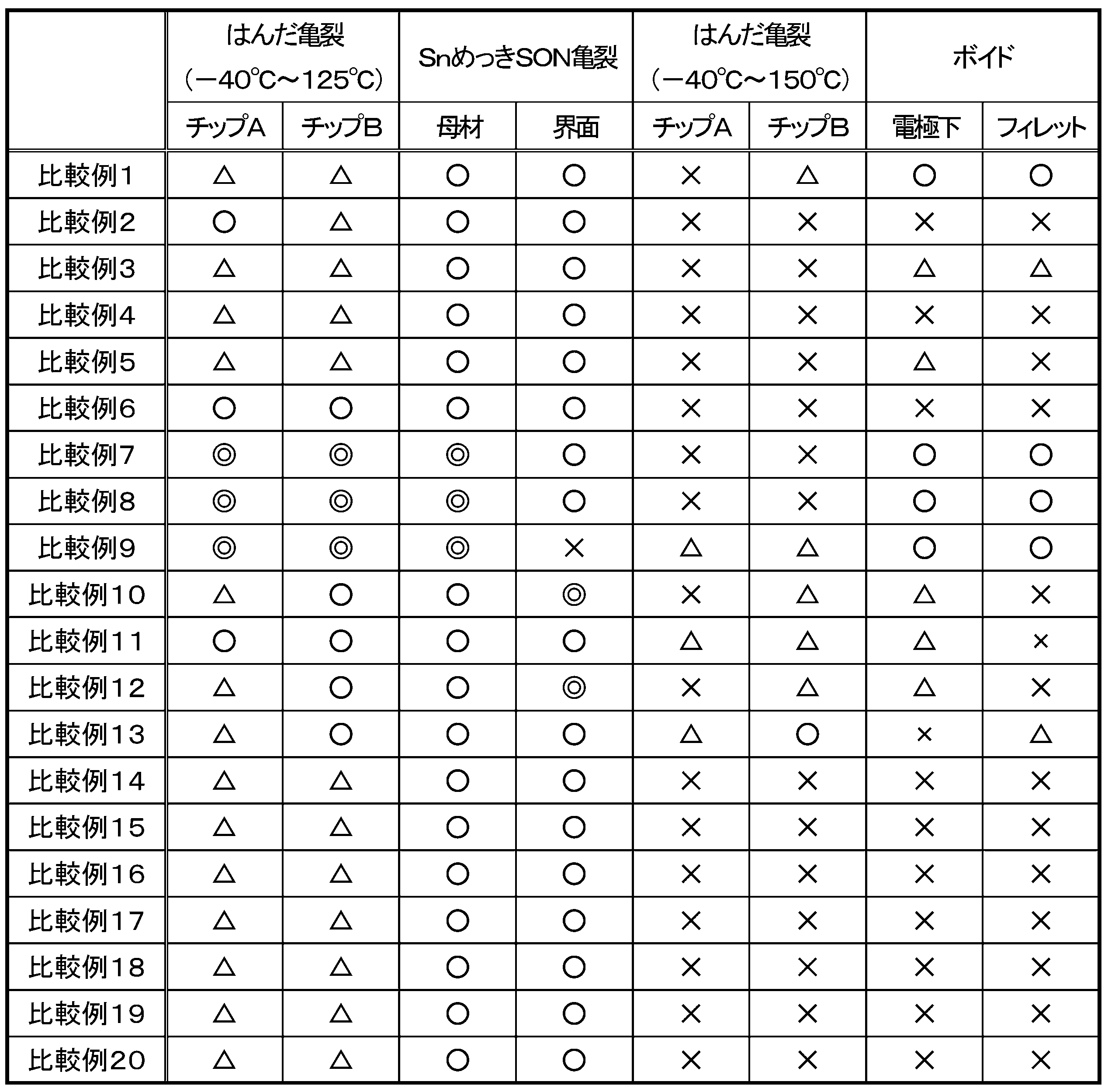
特にNiとCoとを併用した実施例16から実施例33においては、いずれの条件下にあっても良好なはんだ接合部および前記界面付近の亀裂進展抑制効果を発揮し得る。
また、本実施例においては、酸化性の高いBi、Sb、Ni、Co等を一定以上含有させた場合であっても、良好なボイド抑制効果を発揮しつつ、亀裂進展抑制効果を向上することができる。なお例えば実施例17や実施例22のようにNiやCoを0.25質量%含有させた場合であっても、フィレットにおけるボイドの発生を抑制することができる。
更には、実施例15に係る鉛フリーはんだ合金は、酸化性の高いBiを4.5質量%及びSbを5質量%含有させた場合であっても、他の合金元素との組合せ及びこれらの含有バランスにより、亀裂進展抑制効果と共に良好なボイド抑制効果を発揮し得ることが分かる。一方、Biを4.5質量%及びSbを5質量%含有しAgの含有量が4質量%である比較例11に係る鉛フリーはんだ合金では、ボイド試験(4)の結果において、フィレットのボイドは×となっている。
従って、このようなはんだ接合部を有する電子回路基板は車載用電子回路基板といった寒暖差が激しく且つ高い信頼性の求められる電子回路基板にも好適に用いることができる。
更にこのような電子回路基板は、より一層高い信頼性が要求される電子制御装置に好適に使用することができる。
はんだ合金粉末
実施例34:Sn-3.1Ag-0.7Cu-3.2Bi-3Sb-0.03Ni
比較例21:Sn-3.4Ag-0.7Cu-3.2Bi-3Sb-0.03Ni
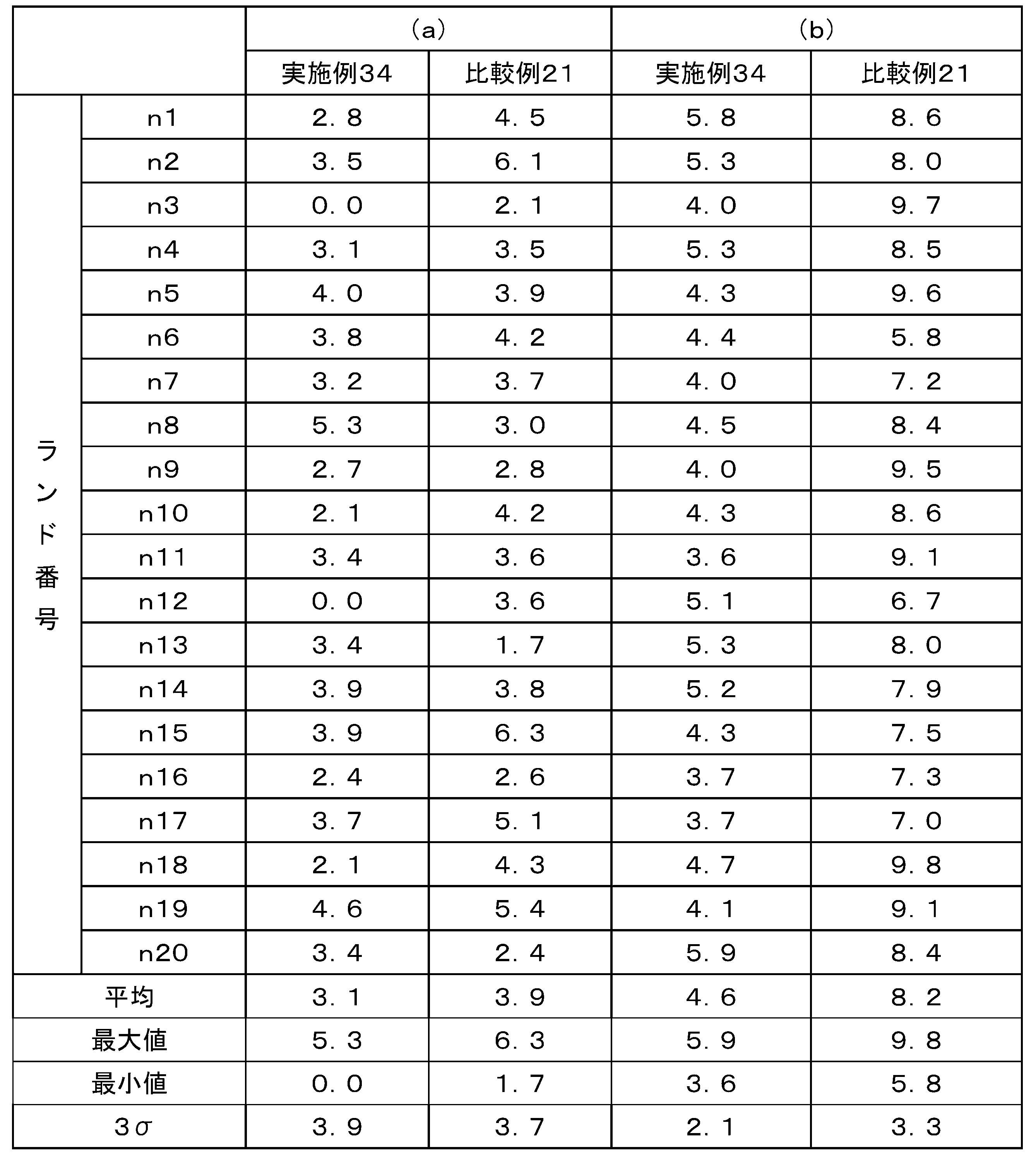
・アクリル樹脂の合成
メタクリル酸10質量%、2-エチルヘキシルメタクリレート51質量%、ラウリルアクリレート39質量%を混合した溶液を作製した。
その後、撹拌機、還流管および窒素導入管とを備えた500mlの4つ口フラスコにジエチルヘキシルグリコール200gを仕込み、これを110℃に加熱した。次いで前記溶液300gにアゾ系ラジカル開始剤としてジメチル2,2’-アゾビス(2-メチルプロピオネート)(製品名:V-601、和光純薬(株)製)を0.2質量%から5質量%を加えてこれを溶解させた。
この溶液を前記4つ口フラスコに1.5時間かけて滴下し、当該4つ口フラスコ内にある成分を110℃で1時間撹拌した後に反応を終了させ、合成樹脂を得た。なお、合成樹脂の重量平均分子量は7,800Mw、酸価は40mgKOH/g、ガラス転移温度は-47℃であった。


※2 日本化成(株)製 ヘキサメチレンビスヒドロキシステアリン酸アマイド
※3 BASFジャパン(株)製 ヒンダードフェノール系酸化防止剤
前記フラックス組成物を11.2質量%と以下のはんだ合金の粉末88.8質量とをそれぞれ混練し、実施例35から46および比較例22から35に係る各ソルダペースト組成物を作製した。
<実施例>
合金(a):Sn-3Ag-0.7Cu-3.5Bi-3Sb-0.04Ni-0.01Coはんだ合金
合金(b):Sn-3Ag-0.5Cu-4.5Bi-3Sb-0.03Niはんだ合金
合金(c):Sn-3Ag-0.5Cu-3.0Bi-2Sb-0.03Niはんだ合金
合金(d):Sn-3Ag-0.7Cu-3.2Bi-3Sb-0.03Ni-0.01Co-0.05Feはんだ合金
<比較例>
合金(a):Sn-3Ag-0.7Cu-3.5Bi-3Sb-0.04Ni-0.01Coはんだ合金
合金(e):Sn-0.5Ag-0.5Cu-3.0Bi-2Sb-0.04Niはんだ合金
※上記はんだ合金粉末の粒径はいずれも20μmから36μmである。
上記ボイド試験(4)と同じ条件にて各試験基板を作製し、同じ条件にて評価した。その結果を表8および表9に表す。
リフロー条件のピーク温度を260℃、200℃以上の時間を70秒間、220℃以上の時間を60秒間とする以外は上記ボイド試験(4)と同じ条件にて各試験基板を作製し、これらを各試験基板の表面状態をX線透過装置(製品名:SMX-160E、(株)島津製作所製)で観察し、チップ部品の周辺および下面に発生したはんだボール数をカウントし、以下のように評価した。その結果を表8および表9にそれぞれ表す。
◎:2.0mm×1.2mmチップ抵抗10個辺りに発生したボール数が0個
○:2.0mm×1.2mmチップ抵抗10個辺りに発生したボール数が0個を超え5個以下
△:2.0mm×1.2mmチップ抵抗10個辺りに発生したボール数が5個を超え10個以下
×:2.0mm×1.2mmチップ抵抗10個辺りに発生したボール数が10個を超える
JIS規格Z 3284(1994)に規定の条件に従い試験を行い、以下のように評価した。その結果を表8および表9にそれぞれ表す。
○:Cu板の変色なし
×:Cu板の変色あり
100ピン0.5mmピッチのBGAを実装できるパターンを有するソルダレジストと電極(直径0.25mm)を備えたガラスエポキシ基板と、同パターンを有する厚さ120μmのメタルマスクを用意した。
前記ガラスエポキシ基板上に前記メタルマスクを用いて各ソルダペースト組成物をそれぞれ6枚連続で印刷し、直径0.25mmにおける転写体積率を画像検査機(製品名:aspire2、(株)コーヨンテクノロジー製)を用いて以下の基準で評価した。その結果を表8および表9にそれぞれ表す。
◎:転写体積率35%以下の個数が0個
○:転写体積率35%以下の個数が0個を超え10個以下
△:転写体積率35%以下の個数が10個を超え50個以下
×:転写体積率35%以下の個数が50個を超える
3.2mm×1.6mmのサイズのチップ部品と、当該サイズのチップ部品を実装できるパターンを有するソルダレジストおよび前記チップ部品を接続する電極(1.6mm×1.2mm)とを備えたガラスエポキシ基板と、同パターンを有する厚さ150μmのメタルマスクを用意した。
前記ガラスエポキシ基板上に前記メタルマスクを用いて各ソルダペースト組成物を印刷し、それぞれ前記チップ部品を搭載し、はんだ接合部を形成した。この際のリフロー条件は、プリヒートを170℃から190℃で110秒間、ピーク温度を245℃とし、200℃以上の時間が65秒間、220℃以上の時間が45秒間、ピーク温度から200℃までの冷却速度を3℃から8℃/秒とし、酸素濃度は1500±500ppmに設定した。
前記はんだ接合部形成後の各ガラスエポキシ基板を-40℃(5分間)から150℃(5分間)の条件に設定した液槽式冷熱衝撃試験装置(製品名:ETAC WINTECH LT80、楠本(株)製)を用いて冷熱衝撃サイクルを1,000、2,000、3,000サイクル繰り返す環境下に曝し、各試験基板を作製した。
次いで各試験基板の対象部分を切り出し、これをエポキシ樹脂(製品名:エポマウント(主剤および硬化剤)、リファインテック(株)製)を用いて封止した。更に湿式研磨機(製品名:TegraPol-25、丸本ストルアス(株)製)を用いて各試験基板に実装された前記チップ部品の中央断面が分かるような状態とし、形成されたはんだ接合部に発生した亀裂がはんだ接合部を完全に横断して破断に至っているか否かを走査電子顕微鏡(製品名:TM-1000、(株)日立ハイテクノロジーズ製)を用いて観察し、以下の基準にて評価した。その結果を表8および表9に表す。なお、各冷熱衝撃サイクルにおける評価チップ数は10個とした。
◎:3,000サイクルまではんだ接合部を完全に横断する亀裂が発生しない
○:2,001から3,000サイクルの間ではんだ接合部を完全に横断する亀裂が発生
△:1,001から2,000サイクルの間ではんだ接合部を完全に横断する亀裂が発生
×:1,000サイクル以下ではんだ接合部を完全に横断する亀裂が発生


2 絶縁層
3 電極部
4 電子部品
5 外部電極
6 はんだ接合部
7 フラックス残渣
8 端部
10 はんだ接合体
100 電子回路基板
Claims (12)
- Agを2質量%以上3.1質量%以下と、Cuを0質量%超1質量%以下と、Sbを1質量%以上5質量%以下と、Biを3.1質量%以上4.5質量%以下と、Niを0.01質量%以上0.25質量%以下含み、残部がSnからなることを特徴とする鉛フリーはんだ合金。
- 更にCoを0.001質量%以上0.25質量%以下含むことを特徴とする請求項1に記載の鉛フリーはんだ合金。
- Agを2質量%以上3.1質量%以下と、Cuを0質量%超1質量%以下と、Sbを1質量%以上5質量%以下と、Biを3.1質量%以上4.5質量%以下と、Niを0.01質量%以上0.25質量%以下と、Coを0.001質量%以上0.25質量%以下含み残部がSnからなり、
AgとCuとSbとBiとNiとCoのそれぞれの含有量(質量%)が下記式(A)から(D)の全てを満たすこと特徴とする鉛フリーはんだ合金。
1.6≦Ag含有量+(Cu含有量/0.5)≦5.9 … A
0.85≦(Ag含有量/3)+(Bi含有量/4.5)≦ 2.10 … B
3.6 ≦ Ag含有量+Sb含有量≦ 8.9 … C
0<(Ni含有量/0.25)+(Co含有量/0.25)≦1.19 …D - 更にInを0質量%超6質量%以下含むことを特徴とする請求項1から請求項3のいずれか1項に記載の鉛フリーはんだ合金。
- 更にP、GaおよびGeの少なくとも1種を合計で0.001質量%以上0.05質量%以下含むことを特徴とする請求項1から請求項4のいずれか1項に記載の鉛フリーはんだ合金。
- 更にFe、Mn、CrおよびMoの少なくとも1種を合計で0.001質量%以上0.05質量%以下含むことを特徴とする請求項1から請求項5のいずれか1項に記載の鉛フリーはんだ合金。
- 請求項1から請求項6のいずれか1項に記載の鉛フリーはんだ合金の粉末と、(A)ベース樹脂と、(B)活性剤と、(C)チキソ剤と、(D)溶剤とを含むフラックス組成物とを含むことを特徴とするソルダペースト組成物。
- 前記フラックス組成物は、前記活性剤(B)の配合量がフラックス組成物全量に対して4.5質量%以上35質量%以下であり、
前記活性剤(B)として、(B-1)炭素数が3から4の直鎖の飽和ジカルボン酸をフラックス組成物全量に対して0.5質量%以上3質量%以下、(B-2)炭素数が5から13のジカルボン酸をフラックス組成物全量に対して2質量%以上15質量%以下、および(B-3)炭素数が20から22のジカルボン酸をフラックス組成物全量に対して2質量%以上15質量%以下含むことを特徴とする請求項7に記載のソルダペースト組成物。 - 前記炭素数が3から4の直鎖の飽和ジカルボン酸(B-1)はマロン酸およびコハク酸の少なくとも一方であり、
前記炭素数が5から13のジカルボン酸(B-2)はグルタル酸、アジピン酸、ピメリン酸、スベリン酸、アゼライン酸、2-メチルアゼライン酸、セバシン酸、ウンデカン二酸、2,4-ジメチル-4-メトキシカルボニルウンデカン二酸、ドデカン二酸、トリデカン二酸および2,4,6-トリメチル-4,6-ジメトキシカルボニルトリデカン二酸から選ばれる少なくとも1種であり、
前記炭素数が20から22のジカルボン酸(B-3)はエイコサ二酸、8-エチルオクタデカン二酸、8,13-ジメチル-8,12-エイコサジエン二酸および11-ビニル-8-オクタデセン二酸から選ばれる少なくとも1種であることを特徴とする請求項8に記載のソルダペースト組成物。 - 請求項1から請求項6のいずれか1項に記載の鉛フリーはんだ合金を用いて形成されるはんだ接合部を有することを特徴とする電子回路基板。
- 請求項7から請求項9のいずれか1項に記載のソルダペースト組成物を用いて形成されるはんだ接合部を有することを特徴とする電子回路基板。
- 請求項10または請求項11に記載の電子回路基板を有することを特徴とする電子制御装置。
Priority Applications (9)
| Application Number | Priority Date | Filing Date | Title |
|---|---|---|---|
| ES17770236T ES2840124T3 (es) | 2016-03-22 | 2017-03-21 | Aleación de soldadura sin plomo, composición de fundente, composición de pasta de soldadura, placa de circuitos electrónicos y controlador electrónico |
| BR112018068596-8A BR112018068596A2 (pt) | 2016-03-22 | 2017-03-21 | liga de soldas sem chumbo, composição de fluxo, composição de pasta de solda, placa de circuito eletrônico, e controlador eletrônico |
| CN201780001047.1A CN107427969B (zh) | 2016-03-22 | 2017-03-21 | 无铅软钎料合金、助焊剂组合物、焊膏组合物、电子电路基板和电子控制装置 |
| EP17770236.2A EP3321025B1 (en) | 2016-03-22 | 2017-03-21 | Lead-free solder alloy, flux composition, solder paste composition, electronic circuit board and electronic control device |
| MX2018011176A MX2018011176A (es) | 2016-03-22 | 2017-03-21 | Aleacion de soldadura sin plomo, composicion de fundente, composicion de pasta de soldadura, placa de circuitos electronicos y controlador electronico. |
| KR1020187000900A KR101925760B1 (ko) | 2016-03-22 | 2017-03-21 | 납 프리 땜납 합금, 플럭스 조성물, 솔더 페이스트 조성물, 전자 회로 기판 및 전자 제어 장치 |
| PH1/2018/500431A PH12018500431B1 (en) | 2016-03-22 | 2017-03-21 | Lead-free solder alloy, flux composition, solder paste composition, electronic circuit board and electronic control device |
| KR1020187000028A KR102052448B1 (ko) | 2016-03-22 | 2017-03-21 | 납 프리 땜납 합금, 플럭스 조성물, 솔더 페이스트 조성물, 전자 회로 기판 및 전자 제어 장치 |
| US15/709,424 US10926360B2 (en) | 2016-03-22 | 2017-09-19 | Lead-free solder alloy, solder joint, solder paste composition, electronic circuit board, and electronic device |
Applications Claiming Priority (8)
| Application Number | Priority Date | Filing Date | Title |
|---|---|---|---|
| JP2016057712A JP6047254B1 (ja) | 2016-03-22 | 2016-03-22 | 鉛フリーはんだ合金、電子回路基板および電子制御装置 |
| JP2016-057712 | 2016-03-22 | ||
| JP2016182809A JP6230674B2 (ja) | 2016-09-20 | 2016-09-20 | 鉛フリーはんだ合金、電子回路基板および電子制御装置 |
| JP2016-182809 | 2016-09-20 | ||
| JP2016224592A JP6125084B1 (ja) | 2016-11-17 | 2016-11-17 | 鉛フリーはんだ合金を用いたソルダペースト組成物、電子回路基板および電子制御装置 |
| JP2016-224592 | 2016-11-17 | ||
| JP2017-015245 | 2017-01-31 | ||
| JP2017015245A JP6560272B2 (ja) | 2017-01-31 | 2017-01-31 | ソルダペースト、電子回路基板及び電子制御装置 |
Related Child Applications (1)
| Application Number | Title | Priority Date | Filing Date |
|---|---|---|---|
| US15/709,424 Continuation US10926360B2 (en) | 2016-03-22 | 2017-09-19 | Lead-free solder alloy, solder joint, solder paste composition, electronic circuit board, and electronic device |
Publications (1)
| Publication Number | Publication Date |
|---|---|
| WO2017164194A1 true WO2017164194A1 (ja) | 2017-09-28 |
Family
ID=59899401
Family Applications (1)
| Application Number | Title | Priority Date | Filing Date |
|---|---|---|---|
| PCT/JP2017/011284 Ceased WO2017164194A1 (ja) | 2016-03-22 | 2017-03-21 | 鉛フリーはんだ合金、フラックス組成物、ソルダペースト組成物、電子回路基板および電子制御装置 |
Country Status (10)
| Country | Link |
|---|---|
| US (1) | US10926360B2 (ja) |
| EP (1) | EP3321025B1 (ja) |
| KR (2) | KR101925760B1 (ja) |
| CN (2) | CN107427969B (ja) |
| BR (1) | BR112018068596A2 (ja) |
| ES (1) | ES2840124T3 (ja) |
| HU (1) | HUE052698T2 (ja) |
| MX (1) | MX2018011176A (ja) |
| PH (1) | PH12018500431B1 (ja) |
| WO (1) | WO2017164194A1 (ja) |
Cited By (7)
| Publication number | Priority date | Publication date | Assignee | Title |
|---|---|---|---|---|
| JP2018122323A (ja) * | 2017-01-31 | 2018-08-09 | 株式会社タムラ製作所 | フラックス組成物、ソルダペースト及び電子回路基板 |
| EP3461580A1 (en) * | 2017-09-29 | 2019-04-03 | Panasonic Intellectual Property Management Co., Ltd. | Solder alloy and junction structure using same |
| US20190134758A1 (en) * | 2017-11-09 | 2019-05-09 | Illinois Tool Works Inc. | Low-silver alternative to standard sac alloys for high reliability applications |
| JP2019147190A (ja) * | 2019-04-23 | 2019-09-05 | 株式会社タムラ製作所 | フラックス組成物、ソルダペースト及び電子回路基板 |
| WO2020137535A1 (ja) * | 2018-12-25 | 2020-07-02 | 株式会社タムラ製作所 | 鉛フリーはんだ合金、はんだ接合用材料、電子回路実装基板及び電子制御装置 |
| WO2020241437A1 (ja) * | 2019-05-27 | 2020-12-03 | 千住金属工業株式会社 | はんだ合金、ソルダペースト、はんだボール、ソルダプリフォーム、はんだ継手、車載電子回路、ecu電子回路、車載電子回路装置、およびecu電子回路装置 |
| JP2024150663A (ja) * | 2019-09-02 | 2024-10-23 | アルファ・アセンブリー・ソリューションズ・インコーポレイテッド | 高温超高信頼性合金 |
Families Citing this family (27)
| Publication number | Priority date | Publication date | Assignee | Title |
|---|---|---|---|---|
| BR112018068596A2 (pt) | 2016-03-22 | 2019-02-12 | Tamura Corporation | liga de soldas sem chumbo, composição de fluxo, composição de pasta de solda, placa de circuito eletrônico, e controlador eletrônico |
| JP6230737B1 (ja) * | 2017-03-10 | 2017-11-15 | 株式会社タムラ製作所 | 鉛フリーはんだ合金、ソルダペースト及び電子回路基板 |
| WO2018181873A1 (ja) | 2017-03-31 | 2018-10-04 | 千住金属工業株式会社 | はんだ合金、ソルダペースト及びはんだ継手 |
| US11732330B2 (en) | 2017-11-09 | 2023-08-22 | Alpha Assembly Solutions, Inc. | High reliability lead-free solder alloy for electronic applications in extreme environments |
| JP6824208B2 (ja) * | 2018-02-26 | 2021-02-03 | 株式会社タムラ製作所 | フラックス及びソルダペースト |
| JP6578393B2 (ja) * | 2018-02-27 | 2019-09-18 | 株式会社タムラ製作所 | 鉛フリーはんだ合金、電子回路実装基板及び電子制御装置 |
| JP6540869B1 (ja) * | 2018-03-30 | 2019-07-10 | 千住金属工業株式会社 | はんだペースト |
| CN108611522B (zh) * | 2018-05-03 | 2020-05-26 | 绍兴市天龙锡材有限公司 | 一种锡合金线 |
| JP7048435B2 (ja) | 2018-06-27 | 2022-04-05 | 株式会社神戸製鋼所 | 積層造形物の積層計画方法、積層造形物の製造方法及び製造装置 |
| CN110883428A (zh) * | 2018-09-10 | 2020-03-17 | 株式会社田村制作所 | 喷射分配器用焊料组合物、及电子基板的制造方法 |
| CN108994480A (zh) * | 2018-10-10 | 2018-12-14 | 云南锡业锡材有限公司 | 一种SnBiAgCu高可靠性无铅焊料合金 |
| TWI725664B (zh) * | 2018-12-14 | 2021-04-21 | 日商千住金屬工業股份有限公司 | 焊料合金、焊料膏、焊料預形體及焊料接頭 |
| CN109698046B (zh) * | 2019-01-15 | 2020-09-15 | 中国科学院电工研究所 | 一种铁基超导加强带及其制备方法 |
| JP6624322B1 (ja) * | 2019-03-27 | 2019-12-25 | 千住金属工業株式会社 | はんだ合金、はんだボール、はんだプリフォーム、はんだペースト及びはんだ継手 |
| JP6810372B1 (ja) * | 2019-05-27 | 2021-01-06 | 千住金属工業株式会社 | はんだ合金、ソルダペースト、はんだボール、ソルダプリフォーム、はんだ継手、および回路 |
| JP6700568B1 (ja) * | 2019-08-09 | 2020-05-27 | 千住金属工業株式会社 | 鉛フリーかつアンチモンフリーのはんだ合金、はんだボール、Ball Grid Arrayおよびはんだ継手 |
| HUE061641T2 (hu) * | 2019-12-10 | 2023-07-28 | Heraeus Deutschland Gmbh & Co Kg | Forrasztópaszta |
| JP6928284B1 (ja) * | 2020-02-14 | 2021-09-01 | 千住金属工業株式会社 | 鉛フリーかつアンチモンフリーのはんだ合金、はんだボール、およびはんだ継手 |
| TWI782423B (zh) * | 2020-04-10 | 2022-11-01 | 日商千住金屬工業股份有限公司 | 焊料合金、焊料粉末、焊膏、焊料球、焊料預成形物及焊料接頭 |
| JP6889387B1 (ja) | 2020-06-23 | 2021-06-18 | 千住金属工業株式会社 | はんだ合金、ソルダペースト、はんだボール、ソルダプリフォーム、はんだ継手、車載電子回路、ecu電子回路、車載電子回路装置、及びecu電子回路装置 |
| JP6836040B1 (ja) * | 2020-07-31 | 2021-02-24 | 千住金属工業株式会社 | はんだ合金 |
| JP7161133B1 (ja) * | 2021-09-30 | 2022-10-26 | 千住金属工業株式会社 | はんだ合金、はんだボール、はんだプリフォーム、はんだペースト及びはんだ継手 |
| JP7161134B1 (ja) * | 2021-09-30 | 2022-10-26 | 千住金属工業株式会社 | はんだ合金、はんだボール、はんだプリフォーム、はんだペースト及びはんだ継手 |
| JP2023060639A (ja) * | 2021-10-18 | 2023-04-28 | Tdk株式会社 | はんだ組成物および電子部品 |
| KR20250041178A (ko) | 2022-08-12 | 2025-03-25 | 센주긴조쿠고교 가부시키가이샤 | 땜납 합금, 땜납 페이스트 및 땜납 조인트 |
| JP7323854B1 (ja) * | 2023-01-12 | 2023-08-09 | 千住金属工業株式会社 | はんだ合金、はんだペースト、はんだボール、はんだプリフォーム、はんだ継手、車載電子回路、ecu電子回路、車載電子回路装置、およびecu電子回路装置 |
| WO2025131329A1 (en) | 2023-12-20 | 2025-06-26 | Alpha Assembly Solutions Inc. | Solder joint comprising a tin alloy and an encapsulant comprising silica particles in an epoxy resin, and electronic device |
Citations (14)
| Publication number | Priority date | Publication date | Assignee | Title |
|---|---|---|---|---|
| JPH05228685A (ja) | 1992-02-21 | 1993-09-07 | Matsushita Electric Ind Co Ltd | 高温はんだ |
| JPH09326554A (ja) | 1996-06-06 | 1997-12-16 | Matsushita Electric Ind Co Ltd | 電子部品接合用電極のはんだ合金及びはんだ付け方法 |
| JP2000190090A (ja) | 1998-12-21 | 2000-07-11 | Senju Metal Ind Co Ltd | 鉛フリ―はんだ合金 |
| JP2000349433A (ja) | 1996-02-09 | 2000-12-15 | Matsushita Electric Ind Co Ltd | はんだ付け方法 |
| JP2003260589A (ja) * | 2002-03-07 | 2003-09-16 | Tokyo Daiichi Shoko:Kk | ソルダペースト用フラックス及びソルダペースト |
| JP2008028413A (ja) | 2007-09-13 | 2008-02-07 | Matsushita Electric Ind Co Ltd | 電子部品のはんだ付け方法 |
| WO2009011341A1 (ja) | 2007-07-13 | 2009-01-22 | Senju Metal Industry Co., Ltd. | 車載実装用鉛フリーはんだと車載電子回路 |
| JP2012081521A (ja) | 2003-04-25 | 2012-04-26 | Cookson Electronics Assembly Materials Group Alpha Metals Loetsysteme Gmbh | Sn、AgおよびCuからなるはんだ物質 |
| JP5324007B1 (ja) * | 2012-06-29 | 2013-10-23 | ハリマ化成株式会社 | はんだ合金、ソルダペーストおよび電子回路基板 |
| JP2014036985A (ja) * | 2012-08-16 | 2014-02-27 | Tamura Seisakusho Co Ltd | はんだ組成物およびそれを用いたプリント配線基板 |
| JP2014054663A (ja) * | 2012-09-13 | 2014-03-27 | Tamura Seisakusho Co Ltd | フラックス組成物、ソルダーペースト組成物及びプリント配線基板 |
| JP2014065065A (ja) * | 2012-09-26 | 2014-04-17 | Tamura Seisakusho Co Ltd | 無鉛はんだ合金、ソルダーペースト組成物及びプリント配線板 |
| WO2014163167A1 (ja) * | 2013-04-02 | 2014-10-09 | 千住金属工業株式会社 | 鉛フリーはんだ合金と車載電子回路 |
| JP6053248B1 (ja) * | 2015-07-24 | 2016-12-27 | ハリマ化成株式会社 | はんだ合金、ソルダペーストおよび電子回路基板 |
Family Cites Families (30)
| Publication number | Priority date | Publication date | Assignee | Title |
|---|---|---|---|---|
| JP3353640B2 (ja) | 1997-04-16 | 2002-12-03 | 富士電機株式会社 | はんだ合金 |
| US20020155024A1 (en) * | 2000-10-27 | 2002-10-24 | H-Technologies Group, Inc. | Lead-free solder compositions |
| TW592872B (en) * | 2001-06-28 | 2004-06-21 | Senju Metal Industry Co | Lead-free solder alloy |
| GB2419137A (en) * | 2004-10-15 | 2006-04-19 | Alpha Fry Ltd | Solder alloy |
| US8888932B2 (en) | 2007-07-18 | 2014-11-18 | Senju Metal Industry Co., Ltd. | Indium-containing lead-free solder for vehicle-mounted electronic circuits |
| JP5230974B2 (ja) | 2007-07-25 | 2013-07-10 | 新日鉄住金マテリアルズ株式会社 | ハンダ合金、ハンダボール及びハンダバンプを有する電子部材 |
| WO2011102034A1 (ja) | 2010-02-16 | 2011-08-25 | 株式会社タムラ製作所 | 鉛フリーはんだ合金と、これを用いたソルダペースト及び実装品 |
| WO2011151894A1 (ja) | 2010-06-01 | 2011-12-08 | 千住金属工業株式会社 | 鉛フリーソルダペースト |
| JP4787384B1 (ja) | 2010-10-29 | 2011-10-05 | ハリマ化成株式会社 | 低銀はんだ合金およびはんだペースト組成物 |
| WO2012127642A1 (ja) * | 2011-03-23 | 2012-09-27 | 千住金属工業株式会社 | 鉛フリーはんだ合金 |
| WO2012131861A1 (ja) * | 2011-03-28 | 2012-10-04 | 千住金属工業株式会社 | 鉛フリーはんだボール |
| JP2013252548A (ja) | 2012-06-08 | 2013-12-19 | Nihon Almit Co Ltd | 微細部品接合用のソルダペースト |
| WO2014013632A1 (ja) | 2012-07-19 | 2014-01-23 | ハリマ化成株式会社 | はんだ合金、ソルダペーストおよび電子回路基板 |
| JP5893528B2 (ja) | 2012-07-27 | 2016-03-23 | 新日鉄住金マテリアルズ株式会社 | 無鉛はんだバンプ接合構造 |
| WO2014097390A1 (ja) * | 2012-12-18 | 2014-06-26 | 千住金属工業株式会社 | 鉛フリーはんだ合金 |
| DE112015000621B4 (de) * | 2014-02-03 | 2024-02-01 | Fuji Electric Co., Ltd. | Flussmittel zum Löten und Lotzusammensetzung |
| WO2015125855A1 (ja) | 2014-02-24 | 2015-08-27 | 株式会社弘輝 | 鉛フリーはんだ合金、はんだ材料及び接合構造体 |
| CN106163732B (zh) | 2014-04-02 | 2019-03-05 | 千住金属工业株式会社 | Led用软钎料合金及led组件 |
| JP6138843B2 (ja) * | 2014-06-27 | 2017-05-31 | 株式会社タムラ製作所 | 鉛フリーはんだ合金含有ソルダペースト組成物、はんだ接合体構造および電子回路基板 |
| JP6383587B2 (ja) * | 2014-06-30 | 2018-08-29 | 株式会社タムラ製作所 | フラックス組成物、はんだ組成物、および電子基板の製造方法 |
| JP5723056B1 (ja) | 2014-12-15 | 2015-05-27 | ハリマ化成株式会社 | はんだ合金、ソルダペーストおよび電子回路基板 |
| US20160279741A1 (en) | 2015-03-24 | 2016-09-29 | Tamura Corporation | Lead-free solder alloy, electronic circuit board, and electronic control device |
| JP6200534B2 (ja) | 2015-03-24 | 2017-09-20 | 株式会社タムラ製作所 | 鉛フリーはんだ合金、電子回路基板および電子制御装置 |
| KR102685941B1 (ko) | 2015-05-05 | 2024-07-17 | 인듐 코포레이션 | 전자장치 적용을 위한 무연 땜납 합금 |
| JP6489037B2 (ja) | 2016-02-10 | 2019-03-27 | 株式会社デンソー | 電子装置及びその製造方法 |
| JP6125084B1 (ja) | 2016-11-17 | 2017-05-10 | 株式会社タムラ製作所 | 鉛フリーはんだ合金を用いたソルダペースト組成物、電子回路基板および電子制御装置 |
| JP6275178B2 (ja) | 2016-03-22 | 2018-02-07 | 株式会社タムラ製作所 | 鉛フリーはんだ合金、電子回路基板および電子制御装置 |
| JP6047254B1 (ja) | 2016-03-22 | 2016-12-21 | 株式会社タムラ製作所 | 鉛フリーはんだ合金、電子回路基板および電子制御装置 |
| BR112018068596A2 (pt) | 2016-03-22 | 2019-02-12 | Tamura Corporation | liga de soldas sem chumbo, composição de fluxo, composição de pasta de solda, placa de circuito eletrônico, e controlador eletrônico |
| JP6275318B1 (ja) | 2017-10-13 | 2018-02-07 | 株式会社タムラ製作所 | 鉛フリーはんだ合金、電子回路基板および電子制御装置 |
-
2017
- 2017-03-21 BR BR112018068596-8A patent/BR112018068596A2/pt not_active Application Discontinuation
- 2017-03-21 PH PH1/2018/500431A patent/PH12018500431B1/en unknown
- 2017-03-21 MX MX2018011176A patent/MX2018011176A/es unknown
- 2017-03-21 KR KR1020187000900A patent/KR101925760B1/ko active Active
- 2017-03-21 KR KR1020187000028A patent/KR102052448B1/ko active Active
- 2017-03-21 EP EP17770236.2A patent/EP3321025B1/en active Active
- 2017-03-21 ES ES17770236T patent/ES2840124T3/es active Active
- 2017-03-21 HU HUE17770236A patent/HUE052698T2/hu unknown
- 2017-03-21 CN CN201780001047.1A patent/CN107427969B/zh active Active
- 2017-03-21 CN CN201810286715.6A patent/CN108500499B/zh active Active
- 2017-03-21 WO PCT/JP2017/011284 patent/WO2017164194A1/ja not_active Ceased
- 2017-09-19 US US15/709,424 patent/US10926360B2/en active Active
Patent Citations (14)
| Publication number | Priority date | Publication date | Assignee | Title |
|---|---|---|---|---|
| JPH05228685A (ja) | 1992-02-21 | 1993-09-07 | Matsushita Electric Ind Co Ltd | 高温はんだ |
| JP2000349433A (ja) | 1996-02-09 | 2000-12-15 | Matsushita Electric Ind Co Ltd | はんだ付け方法 |
| JPH09326554A (ja) | 1996-06-06 | 1997-12-16 | Matsushita Electric Ind Co Ltd | 電子部品接合用電極のはんだ合金及びはんだ付け方法 |
| JP2000190090A (ja) | 1998-12-21 | 2000-07-11 | Senju Metal Ind Co Ltd | 鉛フリ―はんだ合金 |
| JP2003260589A (ja) * | 2002-03-07 | 2003-09-16 | Tokyo Daiichi Shoko:Kk | ソルダペースト用フラックス及びソルダペースト |
| JP2012081521A (ja) | 2003-04-25 | 2012-04-26 | Cookson Electronics Assembly Materials Group Alpha Metals Loetsysteme Gmbh | Sn、AgおよびCuからなるはんだ物質 |
| WO2009011341A1 (ja) | 2007-07-13 | 2009-01-22 | Senju Metal Industry Co., Ltd. | 車載実装用鉛フリーはんだと車載電子回路 |
| JP2008028413A (ja) | 2007-09-13 | 2008-02-07 | Matsushita Electric Ind Co Ltd | 電子部品のはんだ付け方法 |
| JP5324007B1 (ja) * | 2012-06-29 | 2013-10-23 | ハリマ化成株式会社 | はんだ合金、ソルダペーストおよび電子回路基板 |
| JP2014036985A (ja) * | 2012-08-16 | 2014-02-27 | Tamura Seisakusho Co Ltd | はんだ組成物およびそれを用いたプリント配線基板 |
| JP2014054663A (ja) * | 2012-09-13 | 2014-03-27 | Tamura Seisakusho Co Ltd | フラックス組成物、ソルダーペースト組成物及びプリント配線基板 |
| JP2014065065A (ja) * | 2012-09-26 | 2014-04-17 | Tamura Seisakusho Co Ltd | 無鉛はんだ合金、ソルダーペースト組成物及びプリント配線板 |
| WO2014163167A1 (ja) * | 2013-04-02 | 2014-10-09 | 千住金属工業株式会社 | 鉛フリーはんだ合金と車載電子回路 |
| JP6053248B1 (ja) * | 2015-07-24 | 2016-12-27 | ハリマ化成株式会社 | はんだ合金、ソルダペーストおよび電子回路基板 |
Cited By (20)
| Publication number | Priority date | Publication date | Assignee | Title |
|---|---|---|---|---|
| JP2018122323A (ja) * | 2017-01-31 | 2018-08-09 | 株式会社タムラ製作所 | フラックス組成物、ソルダペースト及び電子回路基板 |
| CN109570813B (zh) * | 2017-09-29 | 2021-07-16 | 松下知识产权经营株式会社 | 焊料合金和使用其的接合结构体 |
| EP3461580A1 (en) * | 2017-09-29 | 2019-04-03 | Panasonic Intellectual Property Management Co., Ltd. | Solder alloy and junction structure using same |
| CN109570813A (zh) * | 2017-09-29 | 2019-04-05 | 松下知识产权经营株式会社 | 焊料合金和使用其的接合结构体 |
| US11135683B2 (en) | 2017-09-29 | 2021-10-05 | Panasonic Intellectual Property Management Co., Ltd. | Solder alloy and junction structure using same |
| US11577343B2 (en) * | 2017-11-09 | 2023-02-14 | Alpha Assembly Solutions Inc. | Low-silver alternative to standard SAC alloys for high reliability applications |
| US20190134758A1 (en) * | 2017-11-09 | 2019-05-09 | Illinois Tool Works Inc. | Low-silver alternative to standard sac alloys for high reliability applications |
| US11724341B2 (en) | 2018-12-25 | 2023-08-15 | Tamura Corporation | Lead-free solder alloy, solder joining material, electronic circuit mounting substrate, and electronic control device |
| JP2020099933A (ja) * | 2018-12-25 | 2020-07-02 | 株式会社タムラ製作所 | 鉛フリーはんだ合金、はんだ接合用材料、電子回路実装基板及び電子制御装置 |
| WO2020137535A1 (ja) * | 2018-12-25 | 2020-07-02 | 株式会社タムラ製作所 | 鉛フリーはんだ合金、はんだ接合用材料、電子回路実装基板及び電子制御装置 |
| JP7089491B2 (ja) | 2019-04-23 | 2022-06-22 | 株式会社タムラ製作所 | フラックス組成物、ソルダペースト及び電子回路基板 |
| JP2019147190A (ja) * | 2019-04-23 | 2019-09-05 | 株式会社タムラ製作所 | フラックス組成物、ソルダペースト及び電子回路基板 |
| JP2021037547A (ja) * | 2019-05-27 | 2021-03-11 | 千住金属工業株式会社 | はんだ合金、ソルダペースト、はんだボール、ソルダプリフォーム、はんだ継手、車載電子回路、ecu電子回路、車載電子回路装置、およびecu電子回路装置 |
| CN113874158A (zh) * | 2019-05-27 | 2021-12-31 | 千住金属工业株式会社 | 焊料合金、焊膏、焊球、焊料预制件、焊接接头、车载电子电路、ecu电子电路、车载电子电路装置和ecu电子电路装置 |
| CN113874158B (zh) * | 2019-05-27 | 2022-12-13 | 千住金属工业株式会社 | 焊料合金、焊膏、焊球、焊料预制件、焊接接头 |
| JP6810375B1 (ja) * | 2019-05-27 | 2021-01-06 | 千住金属工業株式会社 | はんだ合金、ソルダペースト、はんだボール、ソルダプリフォーム、はんだ継手、車載電子回路、ecu電子回路、車載電子回路装置、およびecu電子回路装置 |
| WO2020241437A1 (ja) * | 2019-05-27 | 2020-12-03 | 千住金属工業株式会社 | はんだ合金、ソルダペースト、はんだボール、ソルダプリフォーム、はんだ継手、車載電子回路、ecu電子回路、車載電子回路装置、およびecu電子回路装置 |
| US11819955B2 (en) | 2019-05-27 | 2023-11-21 | Senju Metal Industry Co., Ltd. | Solder alloy, solder paste, solder ball, solder preform, solder joint, on-board electronic circuit, ECU electronic circuit, on-board electronic circuit device, and ECU electronic circuit device |
| JP2025061123A (ja) * | 2019-05-27 | 2025-04-10 | 千住金属工業株式会社 | はんだ合金、ソルダペースト、はんだボール、ソルダプリフォーム、はんだ継手、車載電子回路、ecu電子回路、車載電子回路装置、およびecu電子回路装置 |
| JP2024150663A (ja) * | 2019-09-02 | 2024-10-23 | アルファ・アセンブリー・ソリューションズ・インコーポレイテッド | 高温超高信頼性合金 |
Also Published As
| Publication number | Publication date |
|---|---|
| CN107427969B (zh) | 2020-07-07 |
| US20180029169A1 (en) | 2018-02-01 |
| KR20180015711A (ko) | 2018-02-13 |
| ES2840124T3 (es) | 2021-07-06 |
| KR102052448B1 (ko) | 2019-12-05 |
| PH12018500431A1 (en) | 2018-08-29 |
| HUE052698T2 (hu) | 2021-05-28 |
| KR101925760B1 (ko) | 2018-12-05 |
| MX2018011176A (es) | 2019-03-28 |
| EP3321025A4 (en) | 2018-08-22 |
| US10926360B2 (en) | 2021-02-23 |
| CN108500499B (zh) | 2019-10-22 |
| BR112018068596A2 (pt) | 2019-02-12 |
| EP3321025B1 (en) | 2020-11-25 |
| KR20180008883A (ko) | 2018-01-24 |
| PH12018500431B1 (en) | 2023-07-12 |
| CN108500499A (zh) | 2018-09-07 |
| EP3321025A1 (en) | 2018-05-16 |
| CN107427969A (zh) | 2017-12-01 |
Similar Documents
| Publication | Publication Date | Title |
|---|---|---|
| CN108500499B (zh) | 无铅软钎料合金、电子电路基板和电子控制装置 | |
| JP6677668B2 (ja) | 鉛フリーはんだ合金、電子回路基板および電子制御装置 | |
| JP6047254B1 (ja) | 鉛フリーはんだ合金、電子回路基板および電子制御装置 | |
| JP6560272B2 (ja) | ソルダペースト、電子回路基板及び電子制御装置 | |
| JP6275178B2 (ja) | 鉛フリーはんだ合金、電子回路基板および電子制御装置 | |
| KR102494488B1 (ko) | 납 프리 땜납 합금, 솔더 페이스트 및 전자 회로 기판 | |
| JP6719443B2 (ja) | 鉛フリーはんだ合金、電子回路実装基板及び電子制御装置 | |
| JP7133397B2 (ja) | 鉛フリーはんだ合金、電子回路基板及び電子制御装置 | |
| JP6275305B2 (ja) | はんだ接合体の形成方法、並びに当該形成方法により形成されたはんだ接合体を有する電子回路基板および電子制御装置 | |
| JP6275318B1 (ja) | 鉛フリーはんだ合金、電子回路基板および電子制御装置 | |
| JP6585554B2 (ja) | 鉛フリーはんだ合金、電子回路基板及び電子制御装置 | |
| JP6125084B1 (ja) | 鉛フリーはんだ合金を用いたソルダペースト組成物、電子回路基板および電子制御装置 | |
| JP6230674B2 (ja) | 鉛フリーはんだ合金、電子回路基板および電子制御装置 | |
| JP6795630B2 (ja) | 鉛フリーはんだ合金、ソルダペースト組成物、電子回路基板および電子制御装置 | |
| KR102373856B1 (ko) | 납 프리 땜납 합금, 전자 회로 기판 및 전자 제어 장치 | |
| JP6916243B2 (ja) | 鉛フリーはんだ合金、電子回路基板及び電子制御装置 | |
| WO2019053866A1 (ja) | 鉛フリーはんだ合金、電子回路基板及び電子制御装置 | |
| JP2018122322A (ja) | 鉛フリーはんだ合金、ソルダペースト、電子回路基板及び電子制御装置 | |
| JP6467485B2 (ja) | 鉛フリーはんだ合金、電子回路基板および電子制御装置 | |
| JP6467484B2 (ja) | 鉛フリーはんだ合金、電子回路基板および電子制御装置 | |
| KR20210015600A (ko) | 납 프리 땜납 합금, 솔더 페이스트, 전자 회로 실장 기판 및 전자 제어 장치 |
Legal Events
| Date | Code | Title | Description |
|---|---|---|---|
| ENP | Entry into the national phase |
Ref document number: 20187000028 Country of ref document: KR Kind code of ref document: A |
|
| WWE | Wipo information: entry into national phase |
Ref document number: 2017770236 Country of ref document: EP |
|
| WWE | Wipo information: entry into national phase |
Ref document number: 12018500431 Country of ref document: PH |
|
| WWE | Wipo information: entry into national phase |
Ref document number: MX/A/2018/011176 Country of ref document: MX |
|
| NENP | Non-entry into the national phase |
Ref country code: DE |
|
| REG | Reference to national code |
Ref country code: BR Ref legal event code: B01A Ref document number: 112018068596 Country of ref document: BR |
|
| ENP | Entry into the national phase |
Ref document number: 112018068596 Country of ref document: BR Kind code of ref document: A2 Effective date: 20180913 |