WO2017175394A1 - マルチレベル電力変換装置 - Google Patents
マルチレベル電力変換装置 Download PDFInfo
- Publication number
- WO2017175394A1 WO2017175394A1 PCT/JP2016/061584 JP2016061584W WO2017175394A1 WO 2017175394 A1 WO2017175394 A1 WO 2017175394A1 JP 2016061584 W JP2016061584 W JP 2016061584W WO 2017175394 A1 WO2017175394 A1 WO 2017175394A1
- Authority
- WO
- WIPO (PCT)
- Prior art keywords
- circuit
- semiconductor module
- capacitor
- switching element
- bus
- Prior art date
- Legal status (The legal status is an assumption and is not a legal conclusion. Google has not performed a legal analysis and makes no representation as to the accuracy of the status listed.)
- Ceased
Links
Images


Classifications
-
- H—ELECTRICITY
- H10—SEMICONDUCTOR DEVICES; ELECTRIC SOLID-STATE DEVICES NOT OTHERWISE PROVIDED FOR
- H10W—GENERIC PACKAGES, INTERCONNECTIONS, CONNECTORS OR OTHER CONSTRUCTIONAL DETAILS OF DEVICES COVERED BY CLASS H10
- H10W44/00—Electrical arrangements for controlling or matching impedance
- H10W44/601—Capacitive arrangements
-
- H—ELECTRICITY
- H02—GENERATION; CONVERSION OR DISTRIBUTION OF ELECTRIC POWER
- H02M—APPARATUS FOR CONVERSION BETWEEN AC AND AC, BETWEEN AC AND DC, OR BETWEEN DC AND DC, AND FOR USE WITH MAINS OR SIMILAR POWER SUPPLY SYSTEMS; CONVERSION OF DC OR AC INPUT POWER INTO SURGE OUTPUT POWER; CONTROL OR REGULATION THEREOF
- H02M7/00—Conversion of AC power input into DC power output; Conversion of DC power input into AC power output
- H02M7/003—Constructional details, e.g. physical layout, assembly, wiring or busbar connections
-
- H—ELECTRICITY
- H02—GENERATION; CONVERSION OR DISTRIBUTION OF ELECTRIC POWER
- H02M—APPARATUS FOR CONVERSION BETWEEN AC AND AC, BETWEEN AC AND DC, OR BETWEEN DC AND DC, AND FOR USE WITH MAINS OR SIMILAR POWER SUPPLY SYSTEMS; CONVERSION OF DC OR AC INPUT POWER INTO SURGE OUTPUT POWER; CONTROL OR REGULATION THEREOF
- H02M7/00—Conversion of AC power input into DC power output; Conversion of DC power input into AC power output
- H02M7/42—Conversion of DC power input into AC power output without possibility of reversal
- H02M7/44—Conversion of DC power input into AC power output without possibility of reversal by static converters
- H02M7/48—Conversion of DC power input into AC power output without possibility of reversal by static converters using discharge tubes with control electrode or semiconductor devices with control electrode
- H02M7/483—Converters with outputs that each can have more than two voltages levels
- H02M7/487—Neutral point clamped inverters
-
- H—ELECTRICITY
- H10—SEMICONDUCTOR DEVICES; ELECTRIC SOLID-STATE DEVICES NOT OTHERWISE PROVIDED FOR
- H10W—GENERIC PACKAGES, INTERCONNECTIONS, CONNECTORS OR OTHER CONSTRUCTIONAL DETAILS OF DEVICES COVERED BY CLASS H10
- H10W90/00—Package configurations
Definitions
- the present invention relates to a multilevel power conversion device.
- a multilevel power conversion device is constituted by a semiconductor module such as a switching element.
- a three-level power conversion device configured to suppress the circuit inductance of the power conversion circuit, improve maintainability, and reduce the manufacturing cost is disclosed (see Patent Document 1).
- the length of the wiring portion of the power conversion circuit is less flexible due to physical limitations. For this reason, when the inductance of the commutation loop generated when the switching element is turned off increases, the surge voltage increases.
- An object of the present invention is to provide a multilevel power conversion device that is configured by a semiconductor module and that suppresses a surge voltage when a switching element is turned off.
- a multilevel power conversion device is a multilevel power conversion device in which a power conversion circuit is configured by a plurality of semiconductor modules, the first capacitor provided in a positive circuit, and the first capacitor A second capacitor provided in a negative circuit, a first switching element in which a current flows from the positive circuit to an AC circuit, and a first capacitor connected in reverse parallel to the first switching element.
- a power conversion circuit is configured by a plurality of semiconductor modules, the first capacitor provided in a positive circuit, and the first capacitor A second capacitor provided in a negative circuit, a first switching element in which a current flows from the positive circuit to an AC circuit, and a first capacitor connected in reverse parallel to the first switching element.
- the third switching element and the third switching element are connected in series to form an electric path through which a current flows in a direction opposite to the second electric circuit.
- a third electric circuit constituted by a diode; a fourth switching element in which a current flows from the AC circuit to the negative circuit; and a fourth diode connected in anti-parallel to the fourth switching element.
- a plurality of semiconductor modules, wherein the first electric circuit and the fourth electric circuit are either the second electric circuit or the third electric circuit, respectively.
- the one and the commutation loop are arranged adjacent to each other so as to reduce the inductance.
- FIG. 1 is a configuration diagram showing the configuration of the three-level power conversion device according to the first embodiment of the present invention.
- FIG. 2 is a circuit diagram illustrating a configuration of a power conversion circuit of the three-level power conversion device according to the first embodiment.
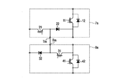
- FIG. 3 is a circuit diagram showing a configuration of an electric circuit of the second semiconductor module and the third semiconductor module according to a modification of the first embodiment.
- FIG. 4 is a side view showing a state in which each semiconductor module according to the first embodiment is connected to a laminate bus.
- FIG. 5 is a configuration diagram showing the configuration of the three-level power conversion device according to the second embodiment of the present invention.
- FIG. 6 is a circuit diagram showing a configuration of a power conversion circuit of the three-level power conversion device according to the second embodiment.
- FIG. 7 is a configuration diagram showing the configuration of the three-level power conversion device according to the third embodiment of the present invention.
- FIG. 8 is a circuit diagram illustrating a configuration of a power conversion circuit of the three-level power conversion device according to the third embodiment.
- FIG. 9 is a circuit diagram showing a configuration of electric circuits of a seventh semiconductor module and an eighth semiconductor module according to a modification of the third embodiment.
- FIG. 10 is a configuration diagram illustrating a configuration of the three-level power conversion device according to the fourth embodiment.
- FIG. 11 is a circuit diagram showing a configuration of a power conversion circuit of the three-level power conversion device according to the fourth embodiment.
- FIG. 12 is a circuit diagram showing a configuration of an electric circuit of the ninth semiconductor module and the tenth semiconductor module according to a modification of the fourth embodiment.
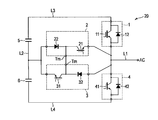
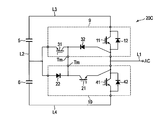
- FIG. 1 is a configuration diagram showing a configuration of a three-level power conversion device 20 according to the first embodiment of the present invention.
- FIG. 2 is a circuit diagram showing a configuration of a power conversion circuit of the three-level power conversion device 20 according to the present embodiment.
- symbol is attached
- the three-level power converter 20 is a neutral point switch type three-level (multi) level inverter.
- the structure for one phase is demonstrated among the three phases of a power converter circuit, all the phases shall be comprised similarly.
- the power conversion circuit may be three-phase or single-phase.
- the three-level power conversion device 20 may be a power conversion device having more than three levels as long as the configuration is the same as that of the present embodiment.
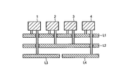
- the three-level power conversion device 20 includes four semiconductor modules 1, 2, 3, 4, two capacitors 5, 6, and four laminate buses L1, L2, L3, L4.
- Laminated buses L1 to L4 are laminated (thin plate shape) conductors.
- the AC bus L1 constitutes an AC circuit of a power conversion circuit and includes an AC terminal.
- the capacitor bus L2 is connected to the two capacitors 5 and 6 and constitutes a capacitor circuit of the power conversion circuit.
- the positive bus L3 constitutes a positive circuit of the power conversion circuit and includes a positive terminal.
- the negative bus L4 constitutes a negative circuit of the power conversion circuit and includes a negative terminal.
- Laminate buses L1 to L4 have a rectangular flat plate shape.
- the AC bus L1 and the capacitor bus L2 have substantially the same shape.
- the positive electrode bus L3 and the negative electrode bus L4 have a shape in which the AC bus L1 or the capacitor bus L2 is substantially halved.
- the side on which the semiconductor modules 1 to 4 and the capacitors 5 and 6 are mounted is the upper side, the AC bus L1, the capacitor bus L2, the positive bus L3, or the negative bus L4 are stacked in order from the top.
- the positive electrode bus L3 and the negative electrode bus L4 are arranged so as to be adjacent side by side without overlapping. Therefore, when the laminated buses L1 to L4 are viewed from the side, the positive electrode bus L3 and the negative electrode bus L4 are contained in one layer. For this reason, the laminate buses L1 to L4 have a total of three layers.
- the laminate buses L1 to L4 are insulated. Note that the order of the laminated buses L1 to L4 to be stacked may be changed in
- the first semiconductor module 1 includes a switching element 11 and a diode 12.
- the diode 12 is connected in antiparallel with the switching element 11. Specifically, the collector (input side) of the switching element 11 and the cathode of the diode 12 are connected, and the emitter (output side) of the switching element 11 and the anode of the diode 12 are connected.
- the cathode of the diode 12 is connected to the positive bus L3.
- the anode of the diode 12 is connected to the AC bus L1.
- the switching element 11 will be described assuming an IGBT (insulated gate bipolar transistor), but other types of switching elements such as a MOSFET (metal oxide semiconductor field-effect transistor) may be used. Further, the other switching elements will be described assuming an IGBT as in the case of the switching element 11, but other types of switching elements may be used.
- the second semiconductor module 2 includes a switching element 21 and a diode 22.
- a diode connected in antiparallel to the switching element 21 may be further provided.
- the switching element 21 is connected in series so that the flowing current is in the same direction as the diode 22 and current is input from the diode 22.
- the collector (input side) of the switching element 21 and the cathode of the diode 22 are connected.
- the anode of the diode 22 is connected to the capacitor bus L2.
- the emitter (output side) of the switching element 21 is connected to the AC bus L1. Thereby, a current path flowing from the capacitor circuit to the AC circuit is formed in the electric circuit of the second semiconductor module 2.
- a terminal Tm connected to the wiring connecting the switching element 21 and the diode 22 is exposed to the outside of the second semiconductor module 2. This terminal Tm is connected to the terminal Tm of the third semiconductor module 3.
- the third semiconductor module 3 includes a switching element 31 and a diode 32.
- a diode connected in antiparallel to the switching element 31 may be further provided.
- the switching element 31 is connected in series so that the direction of the flowing current is the same as that of the diode 32 and current is input from the diode 32.
- the collector (input side) of the switching element 31 and the cathode of the diode 32 are connected.
- the anode of the diode 32 is connected to the AC bus L1. Thereby, a current path flowing from the AC circuit to the capacitor circuit is formed in the electric circuit of the third semiconductor module 3. That is, a current flows in the electric circuit of the third semiconductor module 3 in the opposite direction to the electric circuit of the second semiconductor module 2.
- the emitter (output side) of the switching element 31 is connected to the capacitor bus L2.
- a terminal Tm connected to the wiring connecting the switching element 31 and the diode 32 is exposed to the outside of the third semiconductor module 3. This terminal Tm is connected to the terminal Tm of the second semiconductor module 2.
- the fourth semiconductor module 4 includes a switching element 41 and a diode 42.
- the diode 42 is connected in antiparallel with the switching element 41. Specifically, the collector (input side) of the switching element 41 and the cathode of the diode 42 are connected, and the emitter (output side) of the switching element 41 and the anode of the diode 42 are connected.
- the cathode of the diode 42 is connected to the AC bus L1.
- the anode of the diode 42 is connected to the negative bus L4.
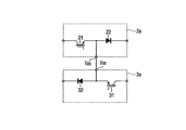
- the second semiconductor module 2 and the third semiconductor module 3 may be replaced with the second semiconductor module 2a and the third semiconductor module 3a according to the modification of the present embodiment shown in FIG. 3, respectively.
- the configuration of the switching element 21a and the diode 22a of the second semiconductor module 2a shown in FIG. 3 is obtained by switching the positions of the switching element 21 and the diode 22 in the second semiconductor module 2 shown in FIG.
- the configuration of the switching element 31a and the diode 32a of the third semiconductor module 3a shown in FIG. 3 is obtained by switching the positions of the switching element 31 and the diode 32 in the third semiconductor module 3 shown in FIG.
- Capacitors 5 and 6 are cylindrical.
- the capacitor 5 is a positive side capacitor provided in the positive circuit.
- the capacitor 6 is a negative side capacitor provided in the negative circuit.
- the capacitors 5 and 6 are connected in series by a capacitor bus L2.
- Each of the capacitors 5 and 6 may be composed of one capacitor or a plurality of unit capacitors.
- the semiconductor modules 1 to 4 and the capacitors 5 and 6 are arranged on the surface of the AC bus L1 in the uppermost layer.
- the first semiconductor module 1, the second semiconductor module 2, the third semiconductor module 3, and the fourth semiconductor module 4 are arranged in a horizontal row in this order.
- Capacitors 5 and 6 are arranged side by side in a separate row from semiconductor modules 1 to 4. Since the semiconductor module 1 and the capacitor 5 are elements connected to the positive bus L3, the semiconductor module 1 and the capacitor 5 are arranged so as to be positioned on the positive bus L3. Since the semiconductor module 4 and the capacitor 6 are elements connected to the negative electrode bus L4, the semiconductor module 4 and the capacitor 6 are arranged so as to be positioned on the negative electrode bus L4.
- FIG. 4 is a side sectional view showing a state in which the semiconductor modules 1 to 4 are connected to the laminate buses L1 to L4, respectively.
- the first semiconductor module 1 is wired to the AC bus L1 and the positive bus L3.
- the AC bus L1 is in the uppermost layer.
- the AC terminal of the first semiconductor module 1 is connected to the surface of the AC bus L1 under the first semiconductor module 1.
- the positive electrode bus L3 is in the lowermost layer.
- the positive terminal of the first semiconductor module 1 passes through the AC bus L1 and the capacitor bus L2, and is connected when it reaches the positive bus L3.
- the AC bus L1 and the capacitor bus L2 are provided so that holes for passing the positive terminal of the first semiconductor module 1 overlap each other. These holes are subjected to insulation treatment so as not to be short-circuited even if the positive electrode terminal of the first semiconductor module 1 contacts.
- holes necessary for passing the terminals of the other semiconductor modules 2 to 4 are also provided in the AC bus L1 or the capacitor bus L2.
- the other semiconductor modules 2 to 4 are also wired in the same manner as the first semiconductor module 1.
- the second semiconductor module 2 and the third semiconductor module 3 are wired to the AC bus L1 and the capacitor bus L2.
- the fourth semiconductor module 4 is wired to the AC bus L1 and the negative bus L4.
- the second semiconductor module 2 and the third semiconductor module 3 are connected to each other by a terminal Tm.
- the capacitors 5 and 6 are provided with holes necessary for passing the terminals through the AC bus L1 and the capacitor bus L2, and are wired to the positive bus L3 or the negative bus L4 and the capacitor bus L2.
- the semiconductor modules 1 to 4 are arranged so that the inductance of the circuit through which the positive current flows is reduced during the zero or positive AC voltage period. This reduces the inductance of the commutation loop when the switching elements 11, 21, 31, and 41 of the semiconductor modules 1 to 4 are turned off.
- the current flowing through the commutation loop is such that the current from the AC side of the first semiconductor module 1 enters from the second semiconductor module 2 and the current from the AC side of the third semiconductor module 3 is the fourth. It flows through the path entering the semiconductor module 4.
- the first semiconductor module 1 is disposed adjacent to the second semiconductor module 2 so that the inductance of the path between the first semiconductor module 1 and the second semiconductor module 2 is reduced.
- the third semiconductor module 3 is disposed adjacent to the fourth semiconductor module 4 so that the inductance of the path between the third semiconductor module 3 and the fourth semiconductor module 4 is reduced.
- the first semiconductor module 1 and the second semiconductor module 2 are arranged so as to be adjacent to each other horizontally, but may be arranged so as to be adjacent vertically.
- the third semiconductor module 1 and the fourth semiconductor module 2 may be arranged so as to be vertically adjacent.
- a three-level power conversion circuit that mainly performs reverse conversion rather than forward conversion is configured by four semiconductor modules 1 to 4, and the first semiconductor module 1 and the second semiconductor module 2 are adjacent to each other.
- the third semiconductor module 3 and the fourth semiconductor module 4 adjacent to each other, the inductance of the commutation loop when the switching elements 11 to 41 are turned off can be reduced. As a result, the surge voltage when the switching elements 11 to 41 are off can be suppressed.
- this three-level power conversion circuit may be a circuit that performs only reverse conversion without performing forward conversion.
- the inductance between the positive electrode bus L3 and the negative electrode bus L4 can be increased.
- the elements 11 and 12 connected to the positive bus L3 and the elements 41 and 42 connected to the negative bus L4 are made into separate semiconductor modules 1 and 4, respectively. It arrange
- the positive electrode bus L3 and the negative electrode bus L4 can be accommodated in one layer by arranging the positive electrode bus L3 and the negative electrode bus L4 side by side without overlapping. Thereby, a three-level power converter device can be reduced in size and manufacturing cost can be reduced.
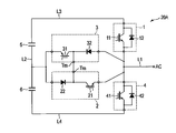
- FIG. 5 is a configuration diagram showing a configuration of a three-level power conversion device 20A according to the second embodiment of the present invention.
- FIG. 6 is a circuit diagram showing a configuration of a power conversion circuit of the three-level power conversion device 20A according to the present embodiment.
- the 3-level power conversion device 20A is obtained by replacing the positions of the second semiconductor module 2 and the third semiconductor module 3 in the 3-level power conversion device 20 according to the first embodiment. That is, the first semiconductor module 1 and the third semiconductor module 3 are disposed adjacent to each other, and the second semiconductor module 2 and the fourth semiconductor module 4 are disposed adjacent to each other.
- the three-level power conversion device 20A mainly performs forward conversion. Other points are the same as in the first embodiment.
- the second semiconductor module 2 and the third semiconductor module 3 may be replaced with the second semiconductor module 2a and the third semiconductor module 3a shown in FIG. 3, respectively.
- a three-level power conversion circuit that mainly performs forward conversion rather than reverse conversion is configured by four semiconductor modules 1 to 4, and the first semiconductor module 1 and the third semiconductor module 3 are adjacent to each other.
- the three-level power conversion circuit may be a circuit that performs only forward conversion without performing reverse conversion.
- FIG. 7 is a configuration diagram showing a configuration of a three-level power conversion device 20B according to the third embodiment of the present invention.
- FIG. 8 is a circuit diagram showing a configuration of a power conversion circuit of the three-level power conversion device 20B according to the present embodiment.
- the three-level power conversion device 20B includes a seventh semiconductor module 7 instead of the first semiconductor module 1 and the second semiconductor module 2 in the three-level power conversion device 20 according to the first embodiment. Instead of the third semiconductor module 3 and the fourth semiconductor module 4, an eighth semiconductor module 8 is provided. Other points are the same as in the first embodiment.
- the seventh semiconductor module 7 is obtained by combining the first semiconductor module 1 and the second semiconductor module 2 according to the first embodiment into one semiconductor module.
- the seventh semiconductor module 7 includes a switching element 11, a diode 12, a switching element 21, and a diode 22.
- the emitter of the switching element 11 is connected to the emitter of the switching element 21. Thereby, the wiring inductance between the electric circuit composed of the switching element 11 and the diode 12 and the electric circuit composed of the switching element 21 and the diode 22 is reduced.
- the other points are the same as the configurations of the first semiconductor module 1 and the second semiconductor module 2 according to the first embodiment.
- the eighth semiconductor module 8 is obtained by combining the third semiconductor module 3 and the fourth semiconductor module 4 into one semiconductor module.
- the eighth semiconductor module 8 includes a switching element 31, a diode 32, a switching element 41, and a diode 42.
- the anode of the diode 32 is connected to the collector of the switching element 41. Thereby, the wiring inductance between the electric circuit composed of the switching element 31 and the diode 32 and the electric circuit composed of the switching element 41 and the diode 42 is reduced.
- the other points are the same as the configurations of the third semiconductor module 3 and the fourth semiconductor module 4.
- the seventh semiconductor module 7 and the eighth semiconductor module 8 may be replaced with the seventh semiconductor module 7a and the eighth semiconductor module 8a according to the modification of the present embodiment shown in FIG. 9, respectively.
- the configuration of the switching element 21a and the diode 22a of the seventh semiconductor module 7a shown in FIG. 9 is the same as the configuration of the second semiconductor module 2a shown in FIG.
- the configuration of the switching element 31a and the diode 32a of the eighth semiconductor module 8a shown in FIG. 9 is the same as the configuration of the third semiconductor module 3a shown in FIG.
- the seventh semiconductor module 7 and the eighth semiconductor module 8 no matter where the semiconductor modules 7 and 8 are arranged, the commutation loop at the time when the switching elements 11 to 41 are turned off. Inductance can be reduced. As a result, the surge voltage when the switching elements 11 to 41 are off can be suppressed.
- FIG. 10 is a configuration diagram showing a configuration of a three-level power conversion device 20C according to the fourth embodiment of the present invention.
- FIG. 11 is a circuit diagram showing a configuration of a power conversion circuit of the three-level power conversion device 20C according to the present embodiment.
- the three-level power conversion device 20C includes a ninth semiconductor module 9 instead of the first semiconductor module 1 and the third semiconductor module 3 in the three-level power conversion device 20A according to the second embodiment.
- a tenth semiconductor module 10 is provided in place of the second semiconductor module 2 and the fourth semiconductor module 4. Other points are the same as in the second embodiment.
- the ninth semiconductor module 9 is obtained by combining the first semiconductor module 1 and the third semiconductor module 3 according to the second embodiment into one semiconductor module.
- the ninth semiconductor module 9 includes a switching element 11, a diode 12, a switching element 31, and a diode 32.
- the emitter of the switching element 11 is connected to the anode of the diode 32.
- the wiring inductance between the electric circuit composed of the switching element 11 and the diode 12 and the electric circuit composed of the switching element 31 and the diode 32 is reduced.
- Other points are the same as the configurations of the first semiconductor module 1 and the third semiconductor module 3 according to the second embodiment.
- the tenth semiconductor module 10 is obtained by combining the second semiconductor module 2 and the fourth semiconductor module 4 into one semiconductor module.
- the tenth semiconductor module 10 includes a switching element 21, a diode 22, a switching element 41, and a diode 42.
- the emitter of the switching element 21 is connected to the collector of the switching element 41.
- the wiring inductance between the electric circuit composed of the switching element 21 and the diode 22 and the electric circuit composed of the switching element 41 and the diode 42 is reduced.
- the other points are the same as the configurations of the second semiconductor module 2 and the fourth semiconductor module 4 according to the second embodiment.
- the ninth semiconductor module 9 and the tenth semiconductor module 10 may be replaced with the ninth semiconductor module 9a and the tenth semiconductor module 10a according to the modification of the present embodiment shown in FIG. 12, respectively.
- the configuration of the switching element 31a and the diode 32a of the ninth semiconductor module 9a shown in FIG. 12 is the same as the configuration of the third semiconductor module 3a shown in FIG.
- the configuration of the switching element 21a and the diode 22a of the tenth semiconductor module 10a shown in FIG. 12 is the same as the configuration of the second semiconductor module 2a shown in FIG.
- the ninth semiconductor module 9 and the tenth semiconductor module 10 no matter where the semiconductor modules 9 and 10 are arranged, the commutation loop at the time when the switching elements 11 to 41 are turned off is provided. Inductance can be reduced. As a result, the surge voltage when the switching elements 11 to 41 are off can be suppressed.
- the present invention is not limited to the above-described embodiment as it is, and can be embodied by modifying constituent elements without departing from the scope of the invention in the implementation stage.
- various inventions can be formed by appropriately combining a plurality of components disclosed in the embodiment. For example, some components may be deleted from all the components shown in the embodiment.
- constituent elements over different embodiments may be appropriately combined.
Landscapes
- Engineering & Computer Science (AREA)
- Power Engineering (AREA)
- Inverter Devices (AREA)
Abstract
Description
図1は、本発明の第1の実施形態に係る3レベル電力変換装置20の構成を示す構成図である。図2は、本実施形態に係る3レベル電力変換装置20の電力変換回路の構成を示す回路図である。なお、図面における同一部分には同一符号を付してその詳しい説明を省略し、異なる部分について主に述べる。
図5は、本発明の第2の実施形態に係る3レベル電力変換装置20Aの構成を示す構成図である。図6は、本実施形態に係る3レベル電力変換装置20Aの電力変換回路の構成を示す回路図である。
図7は、本発明の第3の実施形態に係る3レベル電力変換装置20Bの構成を示す構成図である。図8は、本実施形態に係る3レベル電力変換装置20Bの電力変換回路の構成を示す回路図である。
図10は、本発明の第4の実施形態に係る3レベル電力変換装置20Cの構成を示す構成図である。図11は、本実施形態に係る3レベル電力変換装置20Cの電力変換回路の構成を示す回路図である。
Claims (8)
- 複数の半導体モジュールにより電力変換回路が構成されたマルチレベル電力変換装置であって、
正極回路に設けられた第1のコンデンサと、
前記第1のコンデンサと直列に接続され、負極回路に設けられた第2のコンデンサと、
前記正極回路から交流回路に電流が流れる第1のスイッチング素子及び前記第1のスイッチング素子と逆並列に接続された第1のダイオードにより構成された第1の電気回路と、
前記第1のコンデンサ及び前記第2のコンデンサにより構成されたコンデンサ回路と前記交流回路とを接続する電気経路を形成し、第2のスイッチング素子及び前記第2のスイッチング素子と直列に接続された第2のダイオードにより構成された第2の電気回路と、
前記コンデンサ回路と前記交流回路とを接続し、前記第2の電気回路と逆方向に電流が流れる電気経路を形成し、第3のスイッチング素子及び前記第3のスイッチング素子と直列に接続された第3のダイオードにより構成された第3の電気回路と、
前記交流回路から前記負極回路に電流が流れる第4のスイッチング素子及び前記第4のスイッチング素子と逆並列に接続された第4のダイオードにより構成された第4の電気回路と、
前記交流回路を構成するラミネート化された交流ブスと、
前記交流ブスと積層され、前記コンデンサ回路を構成するラミネート化されたコンデンサブスと、
前記交流ブス及び前記コンデンサブスと積層され、前記正極回路を構成するラミネート化された正極ブスと、
前記交流ブス及び前記コンデンサブスと積層され、前記負極回路を構成するラミネート化された負極ブスとを備え、
複数の半導体モジュールは、前記第1の電気回路及び前記第4の電気回路が、それぞれ前記第2の電気回路又は前記第3の電気回路のいずれ一方と転流ループのインダクタンスが小さくなるように隣接して、配置されたこと
を特徴とするマルチレベル電力変換装置。 - 前記正極ブスは、前記負極ブスと重ならずに、前記交流ブス及び前記コンデンサブスと積層されたこと
を特徴とする請求項1に記載のマルチレベル電力変換装置。 - 前記複数の半導体モジュールは、
前記第1の電気回路が構成された第1の半導体モジュールと、
前記第2の電気回路が構成された第2の半導体モジュールと、
前記第3の電気回路が構成された第3の半導体モジュールと、
前記第4の電気回路が構成された第4の半導体モジュールとを含み、
前記第1の半導体モジュール及び前記第4の半導体モジュールは、それぞれ前記第2の半導体モジュール又は前記第3の半導体モジュールのいずれか一方と隣接するように配置されたこと
を特徴とする請求項1に記載のマルチレベル電力変換装置。 - 前記電力変換回路は、直流電力を交流電力に変換するインバータ動作をし、
前記第2の電気回路は、前記コンデンサ回路から前記交流回路に電流が流れるように構成され、
前記第1の半導体モジュールは、前記第2の半導体モジュールと隣接するように配置され、
前記第4の半導体モジュールは、前記第3の半導体モジュールと隣接するように配置されたこと
を特徴とする請求項3に記載のマルチレベル電力変換装置。 - 前記電力変換回路は、交流電力を直流電力に変換するコンバータ動作をし、
前記第2の電気回路は、前記コンデンサ回路から前記交流回路に電流が流れるように構成され、
前記第1の半導体モジュールは、前記第3の半導体モジュールと隣接するように配置され、
前記第4の半導体モジュールは、前記第2の半導体モジュールと隣接するように配置されたこと
を特徴とする請求項3に記載のマルチレベル電力変換装置。 - 前記複数の半導体モジュールは、
前記第1の電気回路及び前記第2の電気回路が構成された第1の半導体モジュールと、
前記第3の電気回路及び前記第4の電気回路が構成された第2の半導体モジュールとを含むこと
を特徴とする請求項1に記載のマルチレベル電力変換装置。 - 前記電力変換回路は、直流電力を交流電力に変換するインバータ動作をし、
前記第2の電気回路は、前記コンデンサ回路から前記交流回路に電流が流れるように構成されたこと
を特徴とする請求項6に記載のマルチレベル電力変換装置。 - 前記電力変換回路は、交流電力を直流電力に変換するコンバータ動作をし、
前記第2の電気回路は、前記交流回路から前記コンデンサ回路に電流が流れるように構成されたこと
を特徴とする請求項6に記載のマルチレベル電力変換装置。
Priority Applications (6)
| Application Number | Priority Date | Filing Date | Title |
|---|---|---|---|
| EP16897950.8A EP3442108B1 (en) | 2016-04-08 | 2016-04-08 | Multilevel power converter |
| CN201680084098.0A CN109121456B (zh) | 2016-04-08 | 2016-04-08 | 多级电力转换装置 |
| PCT/JP2016/061584 WO2017175394A1 (ja) | 2016-04-08 | 2016-04-08 | マルチレベル電力変換装置 |
| ES16897950T ES2856875T3 (es) | 2016-04-08 | 2016-04-08 | Convertidor de potencia multinivel |
| JP2018510221A JP6573025B2 (ja) | 2016-04-08 | 2016-04-08 | マルチレベル電力変換装置 |
| US16/087,786 US10879814B2 (en) | 2016-04-08 | 2016-04-08 | Multilevel power converter |
Applications Claiming Priority (1)
| Application Number | Priority Date | Filing Date | Title |
|---|---|---|---|
| PCT/JP2016/061584 WO2017175394A1 (ja) | 2016-04-08 | 2016-04-08 | マルチレベル電力変換装置 |
Publications (1)
| Publication Number | Publication Date |
|---|---|
| WO2017175394A1 true WO2017175394A1 (ja) | 2017-10-12 |
Family
ID=60001065
Family Applications (1)
| Application Number | Title | Priority Date | Filing Date |
|---|---|---|---|
| PCT/JP2016/061584 Ceased WO2017175394A1 (ja) | 2016-04-08 | 2016-04-08 | マルチレベル電力変換装置 |
Country Status (6)
| Country | Link |
|---|---|
| US (1) | US10879814B2 (ja) |
| EP (1) | EP3442108B1 (ja) |
| JP (1) | JP6573025B2 (ja) |
| CN (1) | CN109121456B (ja) |
| ES (1) | ES2856875T3 (ja) |
| WO (1) | WO2017175394A1 (ja) |
Cited By (2)
| Publication number | Priority date | Publication date | Assignee | Title |
|---|---|---|---|---|
| DE102023115709A1 (de) * | 2023-06-15 | 2024-12-19 | Semikron Elektronik Gmbh & Co. Kg | Erstes Leistungshalbleitermodul für eine erste Teilschaltung, zweites Leistungshalbleitermodul für eine zweite Teilschaltung und Anordnung hiermit |
| WO2025197474A1 (ja) * | 2024-03-21 | 2025-09-25 | 株式会社デンソー | マルチレベルインバータ |
Families Citing this family (5)
| Publication number | Priority date | Publication date | Assignee | Title |
|---|---|---|---|---|
| CN115315892B (zh) | 2020-03-17 | 2026-04-21 | 华为数字能源技术有限公司 | 用于具有改进的共模性能的输入串联结构的转换器系统的ac/dc转换器级 |
| JP7501164B2 (ja) * | 2020-07-02 | 2024-06-18 | 富士電機株式会社 | 電力変換装置 |
| EP4425780A1 (en) * | 2023-03-03 | 2024-09-04 | Infineon Technologies AG | Semiconductor arrangement and semiconductor module arrangement |
| CN118264079B (zh) * | 2024-03-28 | 2026-02-17 | 漳州科华电气技术有限公司 | 一种多电平电路、印刷电路板和变换器 |
| US20260054579A1 (en) * | 2024-08-22 | 2026-02-26 | BorgWarner US Technologies LLC | Systems for inverter having t-type arrangement for electric vehicle |
Citations (4)
| Publication number | Priority date | Publication date | Assignee | Title |
|---|---|---|---|---|
| JP2011223664A (ja) * | 2010-04-06 | 2011-11-04 | Fuji Electric Co Ltd | パワー半導体モジュール及びそれを用いた電力変換装置 |
| JP2012110095A (ja) * | 2010-11-16 | 2012-06-07 | Fuji Electric Co Ltd | パワー半導体モジュール |
| JP2014217270A (ja) * | 2013-04-23 | 2014-11-17 | ゼミクロン エレクトローニク ゲーエムベーハー ウントコンパニー カーゲー | 3レベル電力変換装置用ハーフブリッジ |
| JP2015091178A (ja) * | 2013-11-06 | 2015-05-11 | 株式会社明電舎 | 3レベル電力変換装置 |
Family Cites Families (12)
| Publication number | Priority date | Publication date | Assignee | Title |
|---|---|---|---|---|
| US9478994B2 (en) * | 2012-07-30 | 2016-10-25 | Obshchestvo S Ogranichennoy Otvetstvennostyu “Sistemy Upravlenia Khraneniem Energii” | Hierarchical system for controlling a battery of electrical energy storage devices |
| JP2014036509A (ja) | 2012-08-09 | 2014-02-24 | Mitsubishi Electric Corp | 3レベル電力変換装置 |
| CN203504422U (zh) * | 2013-07-29 | 2014-03-26 | 特变电工新疆新能源股份有限公司 | 一种用于t型三电平变流器的叠层母排 |
| JP6086157B2 (ja) | 2013-10-02 | 2017-03-01 | 富士電機株式会社 | 3レベルインバータ |
| CN103607131B (zh) * | 2013-12-03 | 2016-01-20 | 上海理工大学 | 三电平逆变器中点电位平衡控制方法 |
| CN204031003U (zh) * | 2014-07-31 | 2014-12-17 | 深圳市英威腾电气股份有限公司 | 一种叠层母排及二极管钳位三电平拓扑装置 |
| JP6160780B2 (ja) | 2014-08-26 | 2017-07-12 | 富士電機株式会社 | 3レベル電力変換装置 |
| CN105450042B (zh) | 2014-09-26 | 2018-04-17 | 台达电子工业股份有限公司 | 三电平功率变换器及其功率单元 |
| CN204316350U (zh) * | 2014-12-30 | 2015-05-06 | 深圳市汇川技术股份有限公司 | T型三电平桥臂模块安装结构以及功率变换器 |
| DE102015115271B4 (de) * | 2015-09-10 | 2021-07-15 | Infineon Technologies Ag | Elektronikbaugruppe mit entstörkondensatoren und verfahren zum betrieb der elektronikbaugruppe |
| JP2018085858A (ja) * | 2016-11-24 | 2018-05-31 | 富士電機株式会社 | 電力変換装置 |
| JP2018107858A (ja) * | 2016-12-22 | 2018-07-05 | 富士電機株式会社 | 電力変換装置 |
-
2016
- 2016-04-08 CN CN201680084098.0A patent/CN109121456B/zh active Active
- 2016-04-08 JP JP2018510221A patent/JP6573025B2/ja active Active
- 2016-04-08 ES ES16897950T patent/ES2856875T3/es active Active
- 2016-04-08 EP EP16897950.8A patent/EP3442108B1/en active Active
- 2016-04-08 WO PCT/JP2016/061584 patent/WO2017175394A1/ja not_active Ceased
- 2016-04-08 US US16/087,786 patent/US10879814B2/en active Active
Patent Citations (4)
| Publication number | Priority date | Publication date | Assignee | Title |
|---|---|---|---|---|
| JP2011223664A (ja) * | 2010-04-06 | 2011-11-04 | Fuji Electric Co Ltd | パワー半導体モジュール及びそれを用いた電力変換装置 |
| JP2012110095A (ja) * | 2010-11-16 | 2012-06-07 | Fuji Electric Co Ltd | パワー半導体モジュール |
| JP2014217270A (ja) * | 2013-04-23 | 2014-11-17 | ゼミクロン エレクトローニク ゲーエムベーハー ウントコンパニー カーゲー | 3レベル電力変換装置用ハーフブリッジ |
| JP2015091178A (ja) * | 2013-11-06 | 2015-05-11 | 株式会社明電舎 | 3レベル電力変換装置 |
Non-Patent Citations (1)
| Title |
|---|
| See also references of EP3442108A4 * |
Cited By (2)
| Publication number | Priority date | Publication date | Assignee | Title |
|---|---|---|---|---|
| DE102023115709A1 (de) * | 2023-06-15 | 2024-12-19 | Semikron Elektronik Gmbh & Co. Kg | Erstes Leistungshalbleitermodul für eine erste Teilschaltung, zweites Leistungshalbleitermodul für eine zweite Teilschaltung und Anordnung hiermit |
| WO2025197474A1 (ja) * | 2024-03-21 | 2025-09-25 | 株式会社デンソー | マルチレベルインバータ |
Also Published As
| Publication number | Publication date |
|---|---|
| US10879814B2 (en) | 2020-12-29 |
| EP3442108B1 (en) | 2020-12-30 |
| EP3442108A1 (en) | 2019-02-13 |
| US20200212821A1 (en) | 2020-07-02 |
| JP6573025B2 (ja) | 2019-09-11 |
| CN109121456A (zh) | 2019-01-01 |
| EP3442108A4 (en) | 2019-11-20 |
| JPWO2017175394A1 (ja) | 2019-01-24 |
| CN109121456B (zh) | 2020-12-04 |
| ES2856875T3 (es) | 2021-09-28 |
Similar Documents
| Publication | Publication Date | Title |
|---|---|---|
| JP6573025B2 (ja) | マルチレベル電力変換装置 | |
| CN105612690B (zh) | 半导体装置 | |
| JP5642086B2 (ja) | 3レベル電力変換装置 | |
| JP5644943B2 (ja) | 半導体モジュール、上下アームキットおよび3レベルインバータ | |
| JP5807516B2 (ja) | 電力変換装置及び電力変換装置における導体の配置方法 | |
| JP2014533487A (ja) | Hブリッジに基づく電力変換器 | |
| JP6196853B2 (ja) | 3レベルコンバータハーフブリッジ | |
| KR101373170B1 (ko) | 컨버터 | |
| JP2014217270A (ja) | 3レベル電力変換装置用ハーフブリッジ | |
| US10164519B2 (en) | Semiconductor stack for converter with snubber capacitors | |
| JP2019162032A (ja) | 半導体ユニット、半導体装置および無停電電源装置 | |
| CN108701689B (zh) | 功率半导体模块 | |
| JP2006166696A (ja) | 寄生インダクタンスの低下されたパワー半導体モジュール | |
| JP5835167B2 (ja) | パワーモジュール構造 | |
| JP5906313B2 (ja) | 電力変換装置 | |
| JP2012170268A (ja) | 半導体スイッチ | |
| JP6268939B2 (ja) | 3レベル電力変換装置 | |
| JP6206090B2 (ja) | 3レベル電力変換装置 | |
| JP4828170B2 (ja) | 電力変換装置 | |
| JP6844932B2 (ja) | 電力変換装置 | |
| JP6573742B2 (ja) | 主回路配線部材及び電力変換装置 |
Legal Events
| Date | Code | Title | Description |
|---|---|---|---|
| WWE | Wipo information: entry into national phase |
Ref document number: 2018510221 Country of ref document: JP |
|
| NENP | Non-entry into the national phase |
Ref country code: DE |
|
| WWE | Wipo information: entry into national phase |
Ref document number: 2016897950 Country of ref document: EP |
|
| ENP | Entry into the national phase |
Ref document number: 2016897950 Country of ref document: EP Effective date: 20181108 |
|
| 121 | Ep: the epo has been informed by wipo that ep was designated in this application |
Ref document number: 16897950 Country of ref document: EP Kind code of ref document: A1 |