WO2017175465A1 - 半導体基板の保護膜形成方法 - Google Patents
半導体基板の保護膜形成方法 Download PDFInfo
- Publication number
- WO2017175465A1 WO2017175465A1 PCT/JP2017/003924 JP2017003924W WO2017175465A1 WO 2017175465 A1 WO2017175465 A1 WO 2017175465A1 JP 2017003924 W JP2017003924 W JP 2017003924W WO 2017175465 A1 WO2017175465 A1 WO 2017175465A1
- Authority
- WO
- WIPO (PCT)
- Prior art keywords
- protective film
- semiconductor substrate
- wafer
- polishing
- film forming
- Prior art date
- Legal status (The legal status is an assumption and is not a legal conclusion. Google has not performed a legal analysis and makes no representation as to the accuracy of the status listed.)
- Ceased
Links
Images




Classifications
-
- H—ELECTRICITY
- H10—SEMICONDUCTOR DEVICES; ELECTRIC SOLID-STATE DEVICES NOT OTHERWISE PROVIDED FOR
- H10P—GENERIC PROCESSES OR APPARATUS FOR THE MANUFACTURE OR TREATMENT OF DEVICES COVERED BY CLASS H10
- H10P14/00—Formation of materials, e.g. in the shape of layers or pillars
- H10P14/60—Formation of materials, e.g. in the shape of layers or pillars of insulating materials
- H10P14/63—Formation of materials, e.g. in the shape of layers or pillars of insulating materials characterised by the formation processes
- H10P14/6326—Deposition processes
- H10P14/6342—Liquid deposition, e.g. spin-coating, sol-gel techniques or spray coating
-
- H—ELECTRICITY
- H10—SEMICONDUCTOR DEVICES; ELECTRIC SOLID-STATE DEVICES NOT OTHERWISE PROVIDED FOR
- H10W—GENERIC PACKAGES, INTERCONNECTIONS, CONNECTORS OR OTHER CONSTRUCTIONAL DETAILS OF DEVICES COVERED BY CLASS H10
- H10W74/00—Encapsulations, e.g. protective coatings
- H10W74/01—Manufacture or treatment
-
- H—ELECTRICITY
- H10—SEMICONDUCTOR DEVICES; ELECTRIC SOLID-STATE DEVICES NOT OTHERWISE PROVIDED FOR
- H10P—GENERIC PROCESSES OR APPARATUS FOR THE MANUFACTURE OR TREATMENT OF DEVICES COVERED BY CLASS H10
- H10P90/00—Preparation of wafers not covered by a single main group of this subclass, e.g. wafer reinforcement
- H10P90/12—Preparing bulk and homogeneous wafers
- H10P90/129—Preparing bulk and homogeneous wafers by polishing
-
- H—ELECTRICITY
- H10—SEMICONDUCTOR DEVICES; ELECTRIC SOLID-STATE DEVICES NOT OTHERWISE PROVIDED FOR
- H10P—GENERIC PROCESSES OR APPARATUS FOR THE MANUFACTURE OR TREATMENT OF DEVICES COVERED BY CLASS H10
- H10P52/00—Grinding, lapping or polishing of wafers, substrates or parts of devices
-
- H—ELECTRICITY
- H10—SEMICONDUCTOR DEVICES; ELECTRIC SOLID-STATE DEVICES NOT OTHERWISE PROVIDED FOR
- H10P—GENERIC PROCESSES OR APPARATUS FOR THE MANUFACTURE OR TREATMENT OF DEVICES COVERED BY CLASS H10
- H10P52/00—Grinding, lapping or polishing of wafers, substrates or parts of devices
- H10P52/40—Chemomechanical polishing [CMP]
- H10P52/402—Chemomechanical polishing [CMP] of semiconductor materials
-
- H—ELECTRICITY
- H10—SEMICONDUCTOR DEVICES; ELECTRIC SOLID-STATE DEVICES NOT OTHERWISE PROVIDED FOR
- H10P—GENERIC PROCESSES OR APPARATUS FOR THE MANUFACTURE OR TREATMENT OF DEVICES COVERED BY CLASS H10
- H10P54/00—Cutting or separating of wafers, substrates or parts of devices
-
- H—ELECTRICITY
- H10—SEMICONDUCTOR DEVICES; ELECTRIC SOLID-STATE DEVICES NOT OTHERWISE PROVIDED FOR
- H10P—GENERIC PROCESSES OR APPARATUS FOR THE MANUFACTURE OR TREATMENT OF DEVICES COVERED BY CLASS H10
- H10P70/00—Cleaning of wafers, substrates or parts of devices
- H10P70/10—Cleaning before device manufacture, i.e. Begin-Of-Line process
- H10P70/15—Cleaning before device manufacture, i.e. Begin-Of-Line process by wet cleaning only
-
- H—ELECTRICITY
- H10—SEMICONDUCTOR DEVICES; ELECTRIC SOLID-STATE DEVICES NOT OTHERWISE PROVIDED FOR
- H10P—GENERIC PROCESSES OR APPARATUS FOR THE MANUFACTURE OR TREATMENT OF DEVICES COVERED BY CLASS H10
- H10P72/00—Handling or holding of wafers, substrates or devices during manufacture or treatment thereof
- H10P72/04—Apparatus for manufacture or treatment
- H10P72/0402—Apparatus for fluid treatment
- H10P72/0406—Apparatus for fluid treatment for cleaning followed by drying, rinsing, stripping, blasting or the like
- H10P72/0411—Apparatus for fluid treatment for cleaning followed by drying, rinsing, stripping, blasting or the like for wet cleaning or washing
- H10P72/0414—Apparatus for fluid treatment for cleaning followed by drying, rinsing, stripping, blasting or the like for wet cleaning or washing using mainly spraying means, e.g. nozzles
-
- H—ELECTRICITY
- H10—SEMICONDUCTOR DEVICES; ELECTRIC SOLID-STATE DEVICES NOT OTHERWISE PROVIDED FOR
- H10P—GENERIC PROCESSES OR APPARATUS FOR THE MANUFACTURE OR TREATMENT OF DEVICES COVERED BY CLASS H10
- H10P72/00—Handling or holding of wafers, substrates or devices during manufacture or treatment thereof
- H10P72/04—Apparatus for manufacture or treatment
- H10P72/0402—Apparatus for fluid treatment
- H10P72/0406—Apparatus for fluid treatment for cleaning followed by drying, rinsing, stripping, blasting or the like
- H10P72/0411—Apparatus for fluid treatment for cleaning followed by drying, rinsing, stripping, blasting or the like for wet cleaning or washing
- H10P72/0416—Apparatus for fluid treatment for cleaning followed by drying, rinsing, stripping, blasting or the like for wet cleaning or washing with the semiconductor substrates being dipped in baths or vessels
-
- H—ELECTRICITY
- H10—SEMICONDUCTOR DEVICES; ELECTRIC SOLID-STATE DEVICES NOT OTHERWISE PROVIDED FOR
- H10P—GENERIC PROCESSES OR APPARATUS FOR THE MANUFACTURE OR TREATMENT OF DEVICES COVERED BY CLASS H10
- H10P72/00—Handling or holding of wafers, substrates or devices during manufacture or treatment thereof
- H10P72/04—Apparatus for manufacture or treatment
- H10P72/0451—Apparatus for manufacturing or treating in a plurality of work-stations
- H10P72/0468—Apparatus for manufacturing or treating in a plurality of work-stations comprising a chamber adapted to a particular process
- H10P72/0472—Apparatus for manufacturing or treating in a plurality of work-stations comprising a chamber adapted to a particular process comprising at least one polishing chamber
Definitions
- the present invention relates to a method for forming a protective film on a semiconductor substrate, and more particularly to a method for forming a protective film on a semiconductor substrate that suppresses adhesion of impurities such as particles, which is formed when the semiconductor substrate is peeled from a polishing head.
- a semiconductor substrate such as a wafer includes a rough polishing / main polishing step, a rinsing step, a hydrophilization step, and a peeling step for peeling the semiconductor substrate from the polishing head by chemical mechanical polishing (CMP).
- CMP chemical mechanical polishing
- the semiconductor substrate is manufactured through a cleaning process for cleaning the polished semiconductor substrate.
- Patent Document 1 As a method for suppressing the adhesion of impurities, for example, in Patent Document 1, a surfactant solution is supplied onto a polishing table simultaneously with a slurry as an abrasive during polishing, and the polishing surface is covered with a surfactant at the same time as polishing is completed. Therefore, a proposal has been made to improve the removal efficiency of particles on the wafer surface in the post-process cleaning.
- the impurity adhesion suppressing method described in Patent Document 1 will be described with reference to FIG. As shown in FIG. 13, in this method for suppressing impurity adhesion, a surfactant solution is discharged from the surfactant nozzle 4 to cover the back surface of the wafer W, and a protective film is further formed.
- the protective film is formed by covering the surface of the wafer W with a surfactant by causing the nozzle 7 to flow over the polishing table 5. That is, the impurity adhesion suppression method described in Patent Document 1 is intended to suppress impurity adhesion by forming protective films of the surfactant solution on the front and back surfaces of the wafer W.
- the wafer W is taken out from the wafer cassette 2 by the loader 1 shown in FIG. 13, and the arm 1 a of the loader 1 is rotated and conveyed to the bottom of the wafer holding unit (polishing head) 3.
- the wafer W is held by the loader 1 so that the back surface thereof faces upward, and the surfactant solution is discharged from the surfactant nozzle 4 to wet the back surface of the wafer W, thereby forming a protective film.
- the wafer holding unit (polishing head) 3 is lowered and the wafer W is mounted.
- the wafer holding unit (polishing head) 3 moves on the polishing table 5 in the direction of the arrow, descends and flows the slurry from the slurry supply nozzle 6, and presses the wafer W against the rotating polishing table 5, and the surface of the wafer W To polish.
- the surfactant solution is allowed to flow from the nozzle 7 onto the polishing table 5 simultaneously with the supply of the slurry, thereby forming a protective film of the surfactant solution on the surface of the wafer W simultaneously with the polishing of the wafer W.
- the wafer holding unit (polishing head) 3 moves up and moves in the direction of the arrow, and again moves down and stops as shown by the arrow. Then, the wafer W is transferred to the arm 8 a of the unloader 8. Next, the arm 8 a of the unloader 8 rotates to store the wafer W in the wafer cassette 11 pulled up from the pure water 10 in the liquid tank 9. Then, the wafer cassette 11 is lowered by an elevator mechanism (not shown), and the polished wafer W is immersed in the pure water 10. Thereafter, the wafer W is transferred to another liquid tank and the wafer W is cleaned.
- the protective film is formed on the back surface and the front surface of the wafer W by supplying the surfactant solution before and during the polishing step.
- the wafer holding unit (polishing head) 3 even if the wafer W is exposed to the air, both the back surface and the front surface of the wafer W are wet with the surfactant solution. (The state in which the protective film is formed) is maintained, and the removal efficiency of particles on the wafer surface is improved in the cleaning process.
- a surfactant is supplied to the back surface of the wafer to form a protective film before polishing.
- the surfactant may adhere to the wafer surface, and a protective film may be partially formed on the wafer surface.
- this protective film is partially formed, there is a technical problem that the surface roughness (Haze) is deteriorated due to a difference in polishing rate between the formed portion and the non-formed portion.
- the surfactant since the surfactant is supplied to the wafer surface during the polishing and the protective film is formed, the protective film is formed on the polished surface during the polishing, and the polishing rate is increased. There was a technical problem that the surface roughness (Haze) deteriorated.
- the protective film is formed on the back surface of the wafer by supplying the surfactant solution before polishing.
- the protective film may be peeled off due to contact between the wafer holding part (polishing head) and the wafer back surface.
- the wafer holding part (polishing head) When the wafer is removed from the wafer holding part (polishing head), particles such as There is a technical problem that impurities easily adhere and the number of LPDs on the back surface of the wafer deteriorates.
- the wafer transferred to the unloader is stored in a wafer cassette and immersed in pure water.
- the protective film is easily peeled off due to the water flow and water pressure when the wafer is immersed in pure water.
- the pure water is applied to the wafer. May collide at a predetermined water pressure, and the protective film of the surfactant formed on the wafer may be peeled off, resulting in a technical problem that the number of LPDs at the part where the protective film is peeled off is deteriorated.
- the present invention has been made to solve the above technical problem, and suppresses a decrease in polishing rate, suppresses adhesion of impurities such as particles, and further suppresses deterioration in the number of LPDs.
- An object is to provide a forming method.
- a method for forming a protective film on a semiconductor substrate comprises a polishing head for holding a semiconductor substrate and a surface plate on which a polishing cloth for polishing the semiconductor substrate is attached. After the polishing process, where the polishing agent is supplied between the polishing cloth and the semiconductor substrate and processed while pressing and sliding the polishing head, the surface of the polished semiconductor substrate is hydrophilized with a surfactant solution. After the first protective film forming step of forming a protective film by performing the treatment, and after the first protective film forming step, the surface of the protective film forming treatment liquid made of a surfactant solution was polished.
- the semiconductor substrate is peeled from the polishing head while at least the surface of the semiconductor substrate is in contact, and the polished semiconductor substrate is immersed in the protective film forming treatment liquid, thereby forming a protective film on the front and back surfaces of the semiconductor substrate.
- It is characterized in that it comprises a second protective film forming step.
- the method for forming a protective film on a semiconductor substrate according to the present invention includes the first protective film forming step and the second protective film forming step as described above. That is, in the present invention, a protective film is not formed before the polishing is completed, and a protective film is formed on the surface of the semiconductor substrate after the polishing is completed, thereby suppressing a decrease in the polishing rate and reducing impurities such as particles. Adhesion can be suppressed and deterioration of the number of LPDs can be suppressed.
- the semiconductor substrate is peeled from the polishing head in a state where at least the surface of the polished semiconductor substrate is in contact, a protective film of a surfactant solution can be immediately formed on the back surface of the semiconductor substrate.
- the adhesion of impurities such as particles can be suppressed, and the deterioration of the number of LPDs can be suppressed.
- the semiconductor substrate it is preferable to peel the semiconductor substrate from the polishing head in a state where the entire semiconductor substrate is immersed in the protective film forming treatment liquid.
- the whole semiconductor substrate peels in the state immersed in the protective film formation process liquid, since the surface and back surface of a semiconductor substrate are not exposed to air
- the semiconductor substrate is peeled off from the polishing head and immersed in a protective film forming treatment liquid comprising a surfactant solution. Therefore, even when the liquid tank is an overflow tank and the surfactant solution collides with the semiconductor substrate at a predetermined water pressure, the surfactant protective film formed during the hydrophilic treatment may be removed. (The protective film of the surfactant is maintained).
- the protective film forming treatment liquid is pure water, the pure water collides with the semiconductor substrate at a predetermined water pressure, so that the protective film of the surfactant formed during the hydrophilic treatment is peeled off. There is a fear and it is not preferable.
- the front and back surfaces of the semiconductor substrate are protected with a protective film, thereby suppressing adhesion of impurities such as particles. And the deterioration of the number of LPDs can be suppressed.
- the concentration of the surfactant in the protective film forming treatment liquid is 1 to 50% by weight. More preferably, it is 30 to 50% by weight. If the concentration is less than 1% by weight, the protective film is not sufficiently formed and the number of large defects (LPD; LightPoint Defects) increases, which is not preferable. On the other hand, if the surfactant is used in excess of 50% by weight, the effect of suppressing the number of LPDs is small, but the cost increases.
- the concentration of the surfactant in the protective film forming treatment liquid is higher than the concentration of the surfactant solution used in the hydrophilization treatment, when the semiconductor substrate is peeled off from the polishing head, it is quickly applied to the back surface of the semiconductor substrate. A protective film can be formed, which is preferable.
- the head body of the polishing head has a recess that opens downward and holds the semiconductor substrate inside, a flow passage for supplying air pressure to the pressurizing space, and the recess is closed.
- a membrane formed of a dish-like elastic material and it is desirable that the pressurization speed to the pressurization space when peeling the semiconductor substrate from the polishing head is 1 to 8 kPa / sec. More preferably, it is 5 to 8 kPa / sec.
- the pressure rate to the pressure space when peeling the semiconductor substrate from the polishing head is 1 to 8 kPa / sec, so that the semiconductor substrate can be peeled from the polishing head more reliably.
- the semiconductor substrate can be immersed in the protective film forming treatment liquid.
- the pressing speed is less than 1 kPa / sec
- the semiconductor substrate cannot be peeled off from the polishing head (membrane) or the semiconductor substrate is peeled off at a low speed. There is a possibility that it cannot be immersed in the forming treatment liquid.
- the pressurization speed exceeds 8 kPa / sec, the membrane may be damaged.
- the present invention it is possible to obtain a method for forming a protective film on a semiconductor substrate that suppresses a decrease in polishing rate, suppresses adhesion of impurities such as particles, and further suppresses deterioration in the number of LPDs.
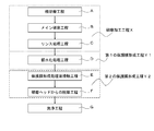
- FIG. 1 is a flowchart showing a method for forming a protective film on a semiconductor substrate according to the present invention.
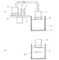
- FIG. 2 is a schematic configuration diagram of a polishing apparatus for explaining the protective film forming step shown in FIG.
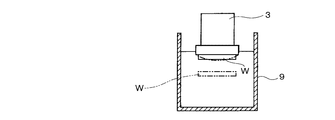
- FIG. 3 is a view showing a modification of the protective film forming step shown in FIG.
- FIG. 4 is a schematic cross-sectional view of the polishing head.
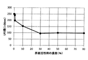
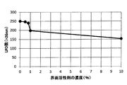
- FIG. 5 is a diagram showing experimental results for verifying the number of LPDs with respect to the surfactant concentration.
- FIG. 6 is an enlarged view of a portion with a surfactant concentration of 0 to 10% in FIG.
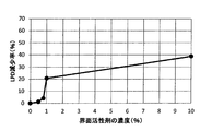
- FIG. 7 is a graph showing the experimental results shown in FIG. 5 in terms of the rate of decrease in the number of LPDs with respect to the surfactant concentration.
- FIG. 8 is an enlarged view of a portion with a surfactant concentration of 0 to 10% in FIG.
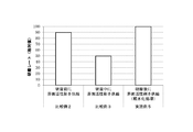
- FIG. 9 is a diagram showing the results of the polishing rates of Example 5 and Comparative Examples 2 and 3.
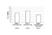
- FIG. 10 is a graph showing the results of surface roughness (Haze) of Example 5 and Comparative Examples 2 and 3.
- FIG. 11 shows a case where the unloader is used (Comparative Example 4) and a case where the wafer is peeled from the polishing head in a state where the wafer surface is in contact with the protective film forming treatment liquid without using the unloader (Example 5). It is a figure which shows the result of the number of LPD.
- FIG. 4 shows a case where the unloader is used (Comparative Example 4) and a case where the wafer is peeled from the polishing head in a state where the wafer surface is in contact with the protective film forming treatment liquid without using the unloader (Example 5). It is a figure which shows the result
- FIG. 12 is a diagram showing the relationship between the pressing speed to the pressing space when the semiconductor substrate is peeled from the polishing head and the number of LPDs on the back surface of the wafer.
- FIG. 13 is a diagram showing a method for manufacturing a semiconductor substrate described in Patent Document 1. In FIG.
- the method for forming a protective film on a semiconductor substrate according to the present invention includes a rough polishing step A, a main polishing step B, and a rinsing step C (a series of steps are referred to as a polishing step X), which are generally polished, This is performed before the cleaning step G for cleaning the substrate.
- the method for forming a protective film on a semiconductor substrate of the present invention includes a first protective film forming process Y1 and a second protective film forming process Y2.
- the first protective film forming step Y1 in the hydrophilic treatment step D for hydrophilizing the wafer without forming a protective film before the polishing is completed, and the hydrophilic treatment step D (first protective film).
- a protective film forming treatment liquid contact step E for bringing the wafer into contact with the protective film forming treatment solution and a second protective film forming step Y2 performed by a peeling step F for peeling the wafer from the polishing head are performed.
- a peeling step F for peeling the wafer from the polishing head
- the first protective film forming step Y1 is a step of forming a protective film on the wafer surface (polished surface), and the number of LPDs on the wafer surface when the wafer is transferred by the protective film, particularly after the polishing is completed. The increase of is suppressed.
- the second protective film forming step Y2 is a step of forming a new protective film on the back surface of the wafer that is exposed when the wafer is peeled off, and an increase in the number of LPDs on the back surface of the wafer is suppressed.
- the number of LPDs is increased not only on the wafer surface but also on the back surface. Can be suppressed.
- FIG. 2 has the same configuration as that of the polishing apparatus shown in FIG. 13, the same or corresponding members are denoted by the same reference numerals, and description thereof is omitted.
- the polishing apparatus shown in FIG. 2 does not include an unloader like the polishing apparatus shown in FIG. 13, and a surfactant solution is applied from the nozzle 7 to the polishing table on the wafer W after the polishing process X is completed. 5 is applied (hydrophilic treatment) to form a protective film of the surfactant solution on the surface of the wafer W (first protective film forming step).
- the wafer W is transferred to the liquid tank 9 by the polishing head 3, and the wafer W is immersed in the protective film forming treatment liquid 12 of the liquid tank 9, and the protective film forming treatment liquid contact process E and the peeling process F are performed.
- the protective film forming treatment liquid 12 is a surfactant solution.
- an overflow tank is used as the liquid tank 9.
- the polishing head 3 (wafer holding portion shown in FIG. 13), a commonly used one can be used. An example is shown in FIG.
- the polishing head 3 shown in FIG. 4 includes a head main body 3A and a rotating shaft 3B.
- the rotating shaft 3B is attached to a conveying means (not shown) and configured to convey the polishing head 3.
- the head body 3A is provided with a recess 3a that opens downward and holds the wafer W inside, and a flow passage 3b that supplies air pressure to the pressurizing space 3A1.
- Reference numeral 3C denotes a membrane, which is attached to the head main body 3A with the recess 3a closed as shown in the figure, and is entirely formed of a substantially dish-like elastic material made of rubber or the like. As a result, a pressurizing space (airtight space) 3A1 is formed in the recess 3a, and the wafer W can be pressed onto the polishing cloth.
- the loader 1 takes out the wafer W from the wafer cassette 2 and rotates the arm 1a of the loader 1 to carry it under the polishing head 3.
- the surfactant solution is not supplied to the back surface of the wafer as in the prior art. This is because if the surfactant solution supplied to the back surface of the wafer adheres to the wafer surface before polishing, the polishing rate partially decreases and the surface roughness (Haze) deteriorates, which is not preferable.
- the polishing head 3 is lowered and the wafer W is mounted.
- the polishing head 3 moves onto the polishing table 5 and presses the wafer W against the rotating polishing table 5 while flowing slurry from the slurry supply nozzle 6 to polish the surface of the wafer W. Further, after the polishing of the wafer W, a rinsing process and a hydrophilization process (first protective film forming process Y1) for covering the surface of the wafer W with a surfactant are performed.
- the hydrophilic treatment step D for hydrophilizing the wafer which is performed before the protective film formation treatment liquid contact step E (second protective film formation step Y2), is performed by polishing cloth for polishing the wafer W, the wafer W, In the meantime, a surfactant solution is supplied as a hydrophilic treatment agent to form a protective film on the wafer surface (polished surface) (first protective film forming step Y1).
- This protective film suppresses an increase in the number of LPDs on the wafer surface, particularly when the wafer is transferred after completion of polishing.
- the polishing head is pressurized at 3 to 6 kPa and the rotation speed of the polishing head is 20 to 40 rpm.
- a protective film is not sufficiently formed on the wafer W by the hydrophilic treatment, which is not preferable.
- the rotation speed of the polishing head is less than 20 rpm, a protective film is not sufficiently formed on the wafer W by the hydrophilic treatment similarly to the above, and when the rotation speed of the polishing head exceeds 40 rpm, it is formed by the hydrophilic treatment. This is not preferable because the formed protective film may be peeled off.
- a surfactant such as a water-soluble anionic surfactant, a water-soluble nonionic surfactant, and a water-soluble amphoteric surfactant is not particularly limited. However, it is preferable to use a water-soluble nonionic surfactant or a water-soluble amphoteric surfactant.
- the water-soluble nonionic activator include dilauric acid polyethylene glycol ester, tridecyl polyoxyethylene ether, nonylphenyl polyoxyethylene ether, polyethylene glycol monostearate and the like.
- the HLB (hydrophilic lipophilic balance) value is 10. The above is preferable.
- Amphoteric surfactants include N-alkylsulfobetaine-modified silicone oil, N-alkylnitrilotriacetic acid, N-alkyldimethylbetaine, ⁇ -trimethylammonio fatty acid, N-alkyl ⁇ -aminopropionic acid, N-alkyl ⁇ -imino Examples thereof include dipropionate, N-alkyloxymethyl-N, N-diethylbetaine, 2-alkylimidazoline derivatives, N-alkylsulfobetaine and the like.
- the concentration of the surfactant solution used for the hydrophilic treatment is preferably 1 to 50% by weight.
- the concentration of the surfactant is less than 1% by weight, a protective film is not sufficiently formed and the number of large defects (LPD; LightPoint Defects) increases, which is not preferable.
- LPD LightPoint Defects
- the surfactant is used in excess of 50% by weight, the effect of suppressing the number of LPDs is small, but the cost increases.
- the polishing head 3 contains the wafer W and the protective film formation treatment liquid 12 as shown in FIG. It is transferred to the liquid tank 9 and placed at a position where at least the surface of the wafer W is in contact with the liquid surface of the protective film forming treatment liquid 12. Thereafter, as shown in FIGS. 2 (b) and 4, air is supplied into the pressurizing space 3A1 so that the pressurizing speed becomes 1 to 8 kPa / sec, and the membrane 3C is curved to project downward. The wafer W is deformed and gradually peeled from the outer peripheral portion of the wafer W toward the center.
- the second protective film forming step Y2 is a step of forming a new protective film on the wafer back surface exposed when the wafer is peeled off, and an increase in the number of LPDs on the wafer back surface is suppressed.
- the wafer can be immersed in the protective film forming treatment liquid 12 simultaneously with the peeling of the wafer W, and the membrane can be prevented from being damaged.
- the wafer W is peeled in the state in which the surface of the wafer W was placed at a position in contact with the liquid surface of the protective film forming treatment liquid 12 was described, as shown in FIG. More preferably, the wafer W is peeled from the polishing head 3 (membrane 3C) in a state where the film is formed in the film forming treatment liquid 12 (a state where the entire wafer W is immersed).
- the entire wafer W is peeled off in the state of being immersed in the protective film forming treatment liquid 12, the front and back surfaces of the wafer W are not exposed to the atmosphere at all, and a protective film can be formed.
- a water-soluble anionic surfactant As the surfactant for the protective film forming treatment liquid, a water-soluble anionic surfactant, a water-soluble nonionic surfactant, and a water-soluble amphoteric surfactant can be used without particular limitation.
- water-soluble nonionic active agents include dilauric acid polyethylene glycol ester, tridecyl polyoxyethylene ether, nonylphenyl polyoxyethylene ether, polyethylene stearate polyethylene glycol, etc., and HLB (hydrophilic lipophilic balance) value. Is preferably 10 or more.
- Amphoteric surfactants include N-alkylsulfobetaine-modified silicone oil, N-alkylnitrilotriacetic acid, N-alkyldimethylbetaine, ⁇ -trimethylammonio fatty acid, N-alkyl ⁇ -aminopropionic acid, N-alkyl ⁇ -imino Examples thereof include dipropionate, N-alkyloxymethyl-N, N-diethylbetaine, 2-alkylimidazoline derivatives, N-alkylsulfobetaine and the like.
- the concentration of the surfactant in the protective film forming treatment liquid is preferably 1 to 50% by weight. More preferably, it is 30 to 50% by weight. If the concentration of the surfactant is less than 1% by weight, a protective film is not sufficiently formed and the number of large defects (LPD; LightPoint Defects) increases, which is not preferable. On the other hand, if the surfactant is used in excess of 50% by weight, the effect of suppressing the number of LPDs is small, but the cost increases.
- LPD LightPoint Defects
- the protection is performed more than the concentration of the hydrophilic treatment solution (surfactant solution) used in the hydrophilic treatment step D (first protective film forming step Y1).
- concentration of the film forming treatment liquid (surfactant solution) is high, a protective film can be quickly formed on the back surface of the wafer when the wafer is peeled from the polishing head, which is preferable.
- the protective film is formed on the semiconductor substrate after completion of polishing without forming the protective film before completion of polishing. Further, since the wafer W is directly put into the liquid tank 9 from the polishing head 3 without transferring the wafer from the polishing head 3 to the arm of the unloader, the conventional contact portion of the wafer W with which the arm contacts is provided. In this case, the protective film of the surfactant (hydrophilic treatment solution) can be prevented from peeling off.
- the wafer W is peeled from the polishing head 3 in a state where at least the surface of the wafer W is in contact with the liquid surface of the protective film forming treatment liquid 12, and the protective film forming treatment liquid (surfactant solution) 12 Soaked. Therefore, the wafer can be immersed in the protective film forming treatment solution simultaneously with the peeling, and the protective film can be quickly formed on the back surface of the wafer.
- the protective film forming treatment liquid surfactant solution
- the liquid tank 9 is an overflow tank, and the protective film forming process is performed on the wafer W. Even when the liquid 12 collides with a predetermined water pressure, there is no possibility that the protective film of the surfactant formed on the wafer W is removed.
- the number of LPDs is increased not only on the wafer surface but also on the back surface. Can be suppressed.
- the semiconductor substrate peeling method according to the present invention can be used for other semiconductor substrates such as single crystal silicon wafers, SiC, and the like. Moreover, it can be applied not only to single-side polishing but also to double-side polishing.
- Examples 1 to 7, Comparative Example 1 A 300 mm diameter single crystal silicon wafer was polished using a general single wafer polishing apparatus.
- the polishing process was performed by the polishing head on which the wafer was mounted moving sequentially on the three polishing tables. Specifically, under the conditions shown in Table 1, a rough polishing step, main (precision) polishing, rinse treatment, and hydrophilic treatment (first protective film forming step) were performed on the polishing table. Note that pure water was used as the rinse treatment liquid.
- the hydrophilization treatment liquid a surfactant solution made of a water-soluble nonionic surfactant having a concentration of 1% by weight was used.
- the process proceeds to the second protective film forming step, and the wafer is peeled from the polishing head in a state where the wafer surface is brought into contact with the overflow protective film forming treatment liquid.
- the pressurization speed at that time was 5 kPa / sec.
- the protective film forming treatment liquid has the same composition as the hydrophilization treatment liquid, and the concentration is 0.5 wt% (Example 1), 0.8 wt% (Example 2), 1 wt% (Example 3). 10% by weight (Example 4), 30% by weight (Example 5), 50% by weight (Example 6), and 80% by weight (Example 7) were used.
- the wafer polished surface was measured with a laser scattering particle counter (Surfscan SP-3 manufactured by KLA-Tencor).
- the measurement area was a range excluding the outer circumference of 3 mm.
- the number of LPDs larger than 26 nm on the silicon wafer was measured.
- the correlation between the measured number of LPDs larger than 26 nm on the silicon wafer and the concentration of the surfactant is shown in FIGS.
- Comparative Example 1 the surface was polished and hydrophilized in the same manner as in Examples 1 to 7, and the wafer surface was in contact with pure water of overflow soot (protective film forming treatment liquid: surfactant 0% by weight). The wafer was peeled off from the polishing head. In the same manner as in Examples 1 to 7, the number of LPDs larger than 26 nm on the silicon wafer was measured. The correlation between the measured number of LPDs larger than 26 nm on the silicon wafer and the concentration of the surfactant is shown in FIGS.
- the concentration of the surfactant as the protective film forming treatment liquid is preferably 0.5 to 50% by weight. More preferably, it is 1 to 50% by weight. More preferably, it is 30 to 50% by weight.
- Example 5 Polishing rate and surface roughness in the case of Example 5, when the surfactant is sprayed on the wafer back surface before polishing (Comparative Example 2), and when the surfactant is supplied during polishing (Comparative Example 3) (Haze) was compared.
- a rough polishing step, main (precision) polishing, rinsing treatment, and hydrophilic treatment (first protective film forming step) were performed on the polishing table under the conditions shown in Table 1 above. It was. Thereafter, the wafer was peeled off from the polishing head and immersed in the overflow soot while the wafer surface was in contact with the protective film forming treatment liquid for the overflow soot.
- a surfactant solution composed of a water-soluble nonionic surfactant having a concentration of 1% by weight is used as the hydrophilic treatment solution, and a protective film forming treatment solution having the same composition as the hydrophilic treatment solution and a concentration of 30% by weight is used. Using. Thereafter, the polishing rate and the surface roughness (Haze) were measured. The polishing rate was calculated by dividing the amount of change in wafer thickness before and after polishing measured by WaferSight (manufactured by KLA-Tencor) by the total time of rough polishing and precision polishing, and was subjected to relative evaluation.
- Comparative Example 2 before polishing, a surfactant made of a water-soluble nonionic surfactant having a concentration of 1% by weight was sprayed on the back surface of the wafer, and the other conditions were the same as in Example 5.
- Comparative Example 3 a surfactant comprising a water-soluble nonionic surfactant having a concentration of 1% by weight was supplied during polishing, and the other conditions were the same as in Example 5.
- the polishing rate and the surface roughness (Haze) were measured in the same manner as in Example 5. The results are shown in FIGS. As is apparent from FIGS.
- the surfactant is supplied in the hydrophilization treatment after polishing rather than the case where the surfactant is supplied before polishing or during polishing (forms the first protective film).
- the surfactant is supplied before polishing or during polishing (forms the first protective film).
- Example 5 Comparative Example 4
- Comparative Example 4 When the unloader shown in the conventional example is used (Comparative Example 4) and when the wafer is peeled from the polishing head in a state where the wafer surface is in contact with the protective film forming treatment liquid without using the unloader (Example 5). Comparison of LPD numbers was performed. Specifically, in Comparative Example 4, after the treatment was performed under the same conditions as in Example 5, the wafer was peeled from the polishing head, the wafer was transferred to an unloader, and immersed in an overflow bowl. Thereafter, the LPD number was measured in the same manner as in Example 5. The results are shown in FIG. 11 together with the results of Example 5.
- a polishing table was subjected to a rough polishing process, main (precision) polishing, rinse treatment, and hydrophilization treatment, and then a water-soluble nonionic activity having a concentration of 1% by weight as a hydrophilization treatment liquid.
- a surfactant solution made of an agent a protective film forming treatment solution having the same composition as the hydrophilization treatment solution and a concentration of 30% by weight was used, and the pressurization rate (1 to 8 kPa / sec) was changed. In this case, the number of LPDs on the back surface of the wafer was examined. The result is shown in FIG.
Landscapes
- Mechanical Treatment Of Semiconductor (AREA)
- Cleaning Or Drying Semiconductors (AREA)
Abstract
Description
ところで、近年、半導体デバイスの高集積化・高密度化に伴い、半導体基板に対するパーティクル等の不純物付着の更なる抑制が求められる。
この不純物付着の抑制方法として、例えば、特許文献1において、研磨中に研磨剤であるスラリーと同時に界面活性剤溶液を研磨テーブル上に供給し、研磨表面を研磨終了と同時に界面活性剤で覆うことによって、後工程の洗浄においてウェーハ表面のパーティクルの除去効率を向上させるという提案がなされている。
図13に示すように、この不純物付着の抑制方法にあっては、界面活性剤ノズル4より界面活性剤溶液を吐出しウェーハWの裏面を覆うことによって保護膜を形成し、更に界面活性剤溶液をノズル7から研磨テーブル5上に流すことにより、ウェーハWの表面を界面活性剤で覆うことによって、保護膜を形成する。
即ち、特許文献1に記載された不純物付着の抑制方法は、前記界面活性剤溶液による保護膜をウェーハWの表面及び裏面に形成することにより、不純物付着の抑制を図るものである。
次に、ウェーハ保持部(研磨ヘッド)3が下降し、ウェーハWを装着する。ウェーハ保持部(研磨ヘッド)3は研磨テーブル5上を矢印の方向に移動し、下降してスラリー供給ノズル6よりスラリーを流しながら、回転する研磨テーブル5にウェーハWを押し付けて、ウェーハWの表面を研磨する。
また、前記スラリーの供給と同時に界面活性剤溶液をノズル7から研磨テーブル5上に流すことにより、ウェーハWの研磨終了と同時にウェーハWの表面を界面活性剤溶液の保護膜を形成する。
次に、アンローダ8のアーム8aが回転し、液槽9の純水10中より引上げられたウェーハカセット11にウェーハWを収納する。そして、図示していないエレベータ機構によりウェーハカセット11を下降させ、研磨が完了したウェーハWを純水10中に浸漬する。その後、別の液槽に搬送され、ウェーハWの洗浄が行われる。
その結果、研磨後、ウェーハ保持部(研磨ヘッド)3でウェーハWを搬送する際に、ウェーハWが空気中に晒されても、ウェーハWの裏面と表面が共に界面活性剤溶液でぬれた状態(保護膜が形成された状態)が維持され、洗浄工程においてウェーハ表面のパーティクルの除去効率が向上する。
また、特許文献1記載の発明にあっては、研磨中に、ウェーハ表面に界面活性剤が供給され、保護膜を形成しているため、研磨中に研磨表面に保護膜が形成され、研磨レートが低下し、表面粗さ(Haze)が悪化するという技術的な課題があった。
しかしながら、研磨加工中に、ウェーハ保持部(研磨ヘッド)とウェーハ裏面との接触によって前記保護膜が剥がれる虞があり、ウェーハ保持部(研磨ヘッド)からウェーハを取り外した際、ウェーハ裏面にパーティクル等の不純物が付着しやすく、ウェーハ裏面のLPD数が悪化するという技術的課題があった。
しかしながら、ウェーハが純水に浸漬される際の水流や水圧によって、前記保護膜は剥がれ易く、特に、前記純水を収容する液槽がオーバーフロー槽である場合には、ウェーハに対して前記純水が所定の水圧で衝突し、ウェーハに形成された界面活性剤の保護膜が剥がれる虞があり、前記保護膜の剥がれた部位のLPD数が悪化するという技術的課題があった。
即ち、本発明にあっては、研磨終了前に保護膜を形成せず、研磨終了後に半導体基板の表面に保護膜を形成することによって、研磨レートの低下を抑制し、またパーティクル等の不純物の付着を抑制し、LPD数の悪化を抑制することができる。
また、本発明では、前記研磨された半導体基板の少なくとも表面が接した状態で、研磨ヘッドから半導体基板が剥離されるため、半導体基板の裏面に界面活性剤溶液の保護膜を直ちに形成することができ、パーティクル等の不純物の付着を抑制することができ、LPD数の悪化を抑制することができる。
そのため、液槽がオーバーフロー槽であって、半導体基板に対して界面活性剤溶液が所定の水圧で衝突した場合でも、親水化処理の際に形成された界面活性剤の保護膜が除去される虞がない(界面活性剤の保護膜が維持される)。尚、保護膜形成処理液が純水である場合には、半導体基板に対して純水が所定の水圧で衝突することにより、親水化処理の際に形成された界面活性剤の保護膜が剥がれる虞があり、好ましくない。
前記濃度が1重量%未満では、十分に保護膜が形成されず大きい欠陥(LPD;LightPoint Defects)の数が増加するため、好ましくない。また、50重量%を超えて界面活性剤を使用すると、LPD数の抑制効果が少ない一方、コストが増大するため、好ましくない。
尚、前記保護膜形成処理液の界面活性剤濃度が、親水化処理で用いられる界面活性剤溶液の濃度よりも高い場合には、研磨ヘッドから半導体基板を剥離する際に半導体基板の裏面に素早く保護膜を形成することができ、好ましい。
このように、研磨ヘッドから半導体基板を剥離する際の加圧空間への加圧速度が1~8kPa/secであることで、より確実に研磨ヘッドから半導体基板を剥離することができ、剥離と同時に半導体基板を保護膜形成処理液に浸漬することができる。
尚、加圧速度が1kPa/sec未満の場合には、研磨ヘッド(メンブレン)から半導体基板を剥離することができない、もしくは、半導体基板を剥離する速度が遅いため、剥離と同時に半導体基板を保護膜形成処理液に浸漬することができない虞がある。一方、加圧速度が8kPa/secを超える場合には、メンブレンが破損する虞がある。
本発明にかかる半導体基板の保護膜形成方法は、一般的になされる粗研磨工程A、メイン研磨工程B、リンス処理工程C(一連の工程を研磨加工工程Xという)の後、研磨された半導体基板を洗浄する洗浄工程Gの前になされる。
具体的には、研磨終了前に保護膜を形成することなく、ウェーハを親水化処理する親水化処理工程Dにおける第1の保護膜形成工程Y1と、親水化処理工程D(第1の保護膜形成工程Y1)の後、保護膜形成処理液にウェーハを接触させる保護膜形成処理液接触工程Eと研磨ヘッドからウェーハを剥離する剥離工程Fによってなされる、第2の保護膜形成工程Y2とを有している。
また、第2の保護膜形成工程Y2は、ウェーハの剥離時に露出するウェーハ裏面に新たな保護膜を形成する工程であって、ウェーハ裏面のLPD数の増加が抑制される。
このように、前記第1の保護膜形成工程Y1及び第2の保護膜形成工程Y2によって、ウェーハ表面、裏面に保護膜を形成することによって、ウェーハ表面だけでなく裏面においてもLPD数の増加を抑制することができる。
この図2に示した研磨装置は、図13に示した研磨装置のようなアンローダを備えておらず、研磨加工工程Xが終了したウェーハWに対して、界面活性剤溶液をノズル7から研磨テーブル5上に流すこと(親水化処理)により、ウェーハWの表面を界面活性剤溶液の保護膜を形成する(第1の保護膜形成工程)。
続いて、前記ウェーハWを研磨ヘッド3によって液槽9に搬送し、ウェーハWを液槽9の保護膜形成処理液12中に浸漬し、前記保護膜形成処理液接触工程Eと前記剥離工程Fとを実行する(第2の保護膜形成工程Y2)。
尚、前記保護膜形成処理液12は、界面活性剤溶液が用いられる。また、液漕9として、オーバーフロー漕が用いられる。
図4に示す研磨ヘッド3は、ヘッド本体3Aと回転軸3Bを備えている。前記回転軸3Bは図示しない搬送手段に取り付けられ、研磨ヘッド3を搬送するように構成されている。
また、符号3Cはメンブレンであって、図に示すように前記凹部3aを閉塞して前記ヘッド本体3Aに取り付けられており、全体がゴム等からなるほぼ皿状の弾性素材によって形成されている。
これにより、前記凹部3a内に加圧空間(気密空間)3A1が形成され、研磨布上にウェーハWを圧接し得るように構成されている。
図2(a)には示していないが、図13に示す場合と同様に、ローダ1によりウェーハカセット2からウェーハWを取出し、ローダ1のアーム1aを回転させ研磨ヘッド3の下まで搬送する。このとき、従来のようにウェーハの裏面に界面活性剤溶液は供給されない。ウェーハの裏面に供給された界面活性剤溶液が研磨前にウェーハ表面に付着すると、部分的に研磨レートが低下し、表面粗さ(Haze)が悪化するため、好ましくないためである。
次に、研磨ヘッド3が下降しウェーハWを装着する。研磨ヘッド3は研磨テーブル5上に移動し、スラリー供給ノズル6よりスラリーを流しながら回転する研磨テーブル5にウェーハWを押し付けてウェーハWの表面を研磨する。
また、ウェーハWの研磨終了後、リンス処理工程、ウェーハWの表面を界面活性剤で覆う親水化処理工程(第1の保護膜形成工程Y1)を行う。
この親水化処理工程Dは、研磨ヘッドを3~6kPaで加圧し、研磨ヘッドの回転数を20~40rpmとすることがより好ましい。
ここで、研磨ヘッドに対する加圧が3kPa未満、または6kPaを超える場合はウェーハW上に十分に親水化処理による保護膜が形成されないため、好ましくない。
また、研磨ヘッドの回転数が20rpm未満の場合は、前記同様にウェーハW上に十分に親水化処理による保護膜が形成されず、研磨ヘッドの回転数が40rpmを超える場合は親水化処理により形成された保護膜が剥がれる虞があるため、好ましくない。
尚、親水化処理に用いられる界面活性剤としては、水溶性陰イオン性界面活性剤、水溶性非イオン活性剤、水溶性両性界面活性剤等の界面活性剤を特に限定されることなく用いることができるが、水溶性非イオン活性剤、水溶性両性界面活性剤を用いることが好ましい。水溶性非イオン活性剤としては、ジラウリン酸ポリエチレングリコールエステル、トリデシルポリオキシエチレンエーテル、ノニルフェニルポリオキシエチレンエーテル、モノステアリン酸ポリエチレングリコール等が挙げられ、HLB(親水性親油性バランス)値が10以上のものが好ましい。両性界面活性剤としては、N-アルキルスルホベタイン変性シリコンオイル、N-アルキルニトリロトリ酢酸、N-アルキルジメチルベタイン、α-トリメチルアンモニオ脂肪酸、N-アルキルβ-アミノプロピオン酸、N-アルキルβ-イミノジプロピオン酸塩、N-アルキルオキシメチル-N,N-ジエチルベタイン、2-アルキルイミダゾリン誘導体、N-アルキルスルホベタイン等が挙げられる。
また、親水化処理に用いられる界面活性剤溶液の濃度は、1~50重量%が好ましい。
前記界面活性剤の濃度が1重量%未満では、十分に保護膜が形成されず大きい欠陥(LPD;LightPoint Defects)の数が増加するため、好ましくない。また、50重量%を超えて界面活性剤を使用すると、LPD数の抑制効果が少ない一方、コストが増大するため、好ましくない。
その後、図2(b)、図4に示すように、加圧速度が1~8kPa/secとなるように加圧空間3A1内にエアを供給し、メンブレン3Cを下方向に突出する湾曲形状に変形させ、ウェーハWの外周部から中心に向かって徐々に剥離する。
この研磨ヘッド3(メンブレン3C)からの剥離によって、ウェーハWは保護膜形成処理液12中に浸漬され、保護膜が形成される(第2の保護膜形成工程Y2)。
このように、第2の保護膜形成工程Y2は、ウェーハの剥離時に露出するウェーハ裏面に新たな保護膜を形成する工程であって、ウェーハ裏面のLPD数の増加が抑制される。
また、ウェーハWの表面が、保護膜形成処理液12の液面に接する位置に置かれた状態で、ウェーハWを剥離する場合について説明したが、図3に示すように、ウェーハW裏面が保護膜形成処理液12に浸漬した状態(ウェーハW全体が浸漬した状態)で、研磨ヘッド3(メンブレン3C)からウェーハWを剥離するのがより好ましい。
ウェーハW全体が保護膜形成処理液12に浸漬した状態で剥離した場合には、ウェーハWの表面及び裏面は大気に全く曝さらされず、保護膜を形成することができる。
好ましくは、水溶性非イオン活性剤として、ジラウリン酸ポリエチレングリコールエステル、トリデシルポリオキシエチレンエーテル、ノニルフェニルポリオキシエチレンエーテル、モノステアリン酸ポリエチレングリコール等が挙げられ、HLB(親水性親油性バランス)値が10以上のものが好ましい。両性界面活性剤としては、N-アルキルスルホベタイン変性シリコンオイル、N-アルキルニトリロトリ酢酸、N-アルキルジメチルベタイン、α-トリメチルアンモニオ脂肪酸、N-アルキルβ-アミノプロピオン酸、N-アルキルβ-イミノジプロピオン酸塩、N-アルキルオキシメチル-N,N-ジエチルベタイン、2-アルキルイミダゾリン誘導体、N-アルキルスルホベタイン等が挙げられる。
前記界面活性剤の濃度が1重量%未満では、十分に保護膜が形成されず大きい欠陥(LPD;LightPoint Defects)の数が増加するため、好ましくない。また、50重量%を超えて界面活性剤を使用すると、LPD数の抑制効果が少ない一方、コストが増大するため、好ましくない。
また、研磨ヘッド3からアンローダのアームにウェーハが移載されることなく、研磨ヘッド3から、液槽9にウェーハWが直接投入されるため、従来のようなアームが接触するウェーハWの接触部における、界面活性剤(親水化処理溶液)の保護膜の剥がれを防止することができる。
そのため、剥離と同時にウェーハを保護膜形成処理液に浸漬することができ、ウェーハ裏面に素早く保護膜を形成することができる。
直径300mm単結晶シリコンウェーハを、一般的な枚葉型研磨装置を用いて研磨した。この実施例で用いた枚葉型研磨装置研磨は、ウェーハを装着した研磨ヘッドが3つの研磨テーブルを順に移動することによって、研磨処理を行った。
具体的には、表1に示す条件下で、研磨テーブルにおいて、粗研磨工程、メイン(精密)研磨、リンス処理、親水化処理(第1の保護膜形成工程)を行った。
尚、リンス処理液としては、純水を用いた。また親水化処理液としては、濃度1重量%の水溶性非イオン活性剤からなる界面活性剤溶液を用いた。
その後、第2の保護膜形成工程に移行し、ウェーハ表面をオーバーフロー漕の保護膜形成処理液に接触させた状態で、研磨ヘッドからウェーハを剥離した。その際の加圧速度は5kPa/secとした。

測定したシリコンウェーハ上の26nmよりも大きいLPD数と界面活性剤の濃度との相関関係を図5~図8に示す。
測定したシリコンウェーハ上の26nmよりも大きいLPD数と界面活性剤の濃度との相関関係を図5~図8に示す。
したがって、保護膜形成処理液としての界面活性剤の濃度は0.5~50重量%が好ましい。より好ましくは1~50重量%が良い。さらに好ましくは、30~50重量%が良い。
前記実施例5の場合と、研磨前にウェーハ裏面に界面活性剤を吹き付けた場合(比較例2)と、研磨中に界面活性剤を供給した場合(比較例3)の研磨レートと表面粗さ(Haze)の比較を行った。
具体的には、実施例5では、上記表1に示す条件下で、研磨テーブルにおいて、粗研磨工程、メイン(精密)研磨、リンス処理、親水化処理(第1の保護膜形成工程)を行った。その後、ウェーハ表面をオーバーフロー漕の保護膜形成処理液に接触させた状態で、研磨ヘッドからウェーハを剥離し、オーバーフロー漕に浸漬した。親水化処理液として、濃度1重量%の水溶性非イオン活性剤からなる界面活性剤溶液を用い、保護膜形成処理液として、親水化処理液と同一組成で、濃度が30重量%のものを用いた。
その後、研磨レートと表面粗さ(Haze)を測定した。研磨レートは、WaferSight(KLA-Tencor社製)で測定した研磨前と研磨後のウェーハ厚さの変化量を粗研磨と精密研磨の合計時間で除することによって算出し、相対評価を行った。また、表面粗さ(Haze)測定は、レーザー散乱パーティクルカウンター(KLA-Tencor社製 Surfscan SP-3)で測定し、実施例5の条件に対する比較例2、3の相対評価を行った。
その結果を図9、図10に示す。
また、比較例3として、研磨中に濃度1重量%の水溶性非イオン活性剤からなる界面活性剤を供給し、それ以外の条件は実施例5と同様に処理を行った。
これら比較例2、比較例3について、実施例5と同様に、研磨レートと表面粗さ(Haze)を測定した。その結果を図9、図10に示す。
図9、図10から明らかなように、研磨前や研磨中に界面活性剤を供給する場合よりも研磨後の親水化処理にて界面活性剤を供給する(第1の保護膜を形成する)ことで、研磨レートの低下と表面粗さの悪化を抑制することができることが認められた。
従来例に示すアンローダを用いた場合(比較例4)と、アンローダを用いることなく、ウェーハ表面を保護膜形成処理液に接触させた状態で研磨ヘッドからウェーハを剥離した場合(実施例5)のLPD数の比較を行った。
具体的には、比較例4では、実施例5と同一条件で処理を行った後、研磨ヘッドから、ウェーハを剥離し、アンローダにウェーハを移載し、オーバーフロー漕に浸漬した。その後、実施例5と同様な方法でLPD数を測定した。その結果を実施例5の結果とともに図11に示す。
一方、ウェーハ表面をオーバーフロー漕の保護膜形成処理液に接触させた場合、ウェーハはアンローダとの接触がなく、ウェーハは保護膜が付着した状態で剥離されるため、LPD数の減少が確認された。
上記表1に示す条件下で、研磨テーブルにおいて、粗研磨工程、メイン(精密)研磨、リンス処理、親水化処理を行った後、親水化処理液として、濃度1重量%の水溶性非イオン活性剤からなる界面活性剤溶液を用い、保護膜形成処理液として、親水化処理液と同一組成で、濃度が30重量%のものを用い、加圧速度(1~8kPa/sec)を変化させた場合のウェーハ裏面のLPD数を調べた。その結果を図12に示す。
また、8kPa/sec超えの場合、メンブレンの破裂が確認された。一方、1~8kPa/secの場合、LPD数の減少が確認され、5~8kPa/secにおいて、より減少していることが確認された。
B メイン研磨工程
C リンス処理工程
D 親水化処理工程
E 保護膜形成処理液接触工程
F 研磨ヘッドからの剥離工程
G 洗浄工程
X 研磨加工工程
Y1 第1の保護膜形成工程
Y2 第2の保護膜形成工程
W ウェーハ
3 研磨ヘッド
9 液槽
12 保護膜形成処理液(界面活性剤溶液)
Claims (3)
- 半導体基板を保持するための研磨ヘッドと、半導体基板を研磨するための研磨布が貼り付けられた定盤を用い、研磨布と半導体基板との間に研磨剤を供給し、研磨ヘッドを加圧・摺動しながら加工する研磨工程の後、
研磨された半導体基板の表面を、界面活性剤溶液による親水化処理を行うことにより保護膜を形成する第1の保護膜形成工程と、
前記第1の保護膜形成工程の後、
界面活性剤溶液からなる保護膜形成処理液の液面に、前記研磨された半導体基板の少なくとも表面が接した状態で、研磨ヘッドから半導体基板が剥離され、
研磨された半導体基板が前記保護膜形成処理液に浸漬されることにより、半導体基板の表面及び裏面に保護膜が形成される第2の保護膜形成工程と、
を含むことを特徴とする半導体基板の保護膜形成方法。 - 前記保護膜形成処理液の界面活性剤濃度が1~50重量%であることを特徴とする請求項1記載の半導体基板の保護膜形成方法。
- 前記研磨ヘッドのヘッド本体には、
下方に開口し、かつ半導体基板を内部に保持するための凹部と、
加圧空間にエア圧を供給するための流通路と、
前記凹部を閉塞して取り付けられ、皿状の弾性素材によって形成されたメンブレンと、を備え、
研磨ヘッドから半導体基板を剥離する際の加圧空間への加圧速度が、1~8kPa/secであることを特徴とする請求項1記載の半導体基板の保護膜形成方法。
Priority Applications (4)
| Application Number | Priority Date | Filing Date | Title |
|---|---|---|---|
| CN201780021006.9A CN108885986B (zh) | 2016-04-04 | 2017-02-03 | 半导体基板的保护膜形成方法 |
| EP17778844.5A EP3442008B1 (en) | 2016-04-04 | 2017-02-03 | Protective film forming method for semiconductor substrate |
| KR1020187029267A KR102172311B1 (ko) | 2016-04-04 | 2017-02-03 | 반도체 기판의 보호막 형성 방법 |
| US16/089,456 US10840089B2 (en) | 2016-04-04 | 2017-02-03 | Protective-film forming method for semiconductor substrate |
Applications Claiming Priority (2)
| Application Number | Priority Date | Filing Date | Title |
|---|---|---|---|
| JP2016-074967 | 2016-04-04 | ||
| JP2016074967A JP6602720B2 (ja) | 2016-04-04 | 2016-04-04 | 半導体基板の保護膜形成方法 |
Publications (1)
| Publication Number | Publication Date |
|---|---|
| WO2017175465A1 true WO2017175465A1 (ja) | 2017-10-12 |
Family
ID=60000979
Family Applications (1)
| Application Number | Title | Priority Date | Filing Date |
|---|---|---|---|
| PCT/JP2017/003924 Ceased WO2017175465A1 (ja) | 2016-04-04 | 2017-02-03 | 半導体基板の保護膜形成方法 |
Country Status (7)
| Country | Link |
|---|---|
| US (1) | US10840089B2 (ja) |
| EP (1) | EP3442008B1 (ja) |
| JP (1) | JP6602720B2 (ja) |
| KR (1) | KR102172311B1 (ja) |
| CN (1) | CN108885986B (ja) |
| TW (1) | TWI614089B (ja) |
| WO (1) | WO2017175465A1 (ja) |
Families Citing this family (2)
| Publication number | Priority date | Publication date | Assignee | Title |
|---|---|---|---|---|
| CN109648451B (zh) | 2018-12-29 | 2020-12-01 | 徐州鑫晶半导体科技有限公司 | 硅晶圆的最终抛光方法和最终抛光装置 |
| JP7812740B2 (ja) * | 2022-05-31 | 2026-02-10 | グローバルウェーハズ・ジャパン株式会社 | シリコンウェーハの研磨方法 |
Citations (5)
| Publication number | Priority date | Publication date | Assignee | Title |
|---|---|---|---|---|
| JPH08197418A (ja) | 1995-01-25 | 1996-08-06 | Nec Corp | ウェハの研磨方法およびその装置 |
| JP2003109931A (ja) * | 2001-09-28 | 2003-04-11 | Sumitomo Mitsubishi Silicon Corp | 半導体ウェーハの洗浄乾燥方法 |
| JP2007050465A (ja) * | 2005-08-17 | 2007-03-01 | Toshiba Corp | 研磨ヘッド、研磨装置及び研磨工具 |
| JP2010021353A (ja) * | 2008-07-10 | 2010-01-28 | Toshiba Corp | 半導体装置の製造方法 |
| JP2013045885A (ja) * | 2011-08-24 | 2013-03-04 | Mitsubishi Materials Techno Corp | 半導体ウェーハの製造方法 |
Family Cites Families (21)
| Publication number | Priority date | Publication date | Assignee | Title |
|---|---|---|---|---|
| JPH0770504B2 (ja) | 1990-12-26 | 1995-07-31 | 信越半導体株式会社 | ウエーハのハンドリング方法及び装置 |
| US5492594A (en) * | 1994-09-26 | 1996-02-20 | International Business Machines Corp. | Chemical-mechanical polishing tool with end point measurement station |
| JP3426866B2 (ja) * | 1996-08-30 | 2003-07-14 | 株式会社東芝 | 半導体装置の製造装置および製造方法 |
| JPH11207594A (ja) * | 1997-11-05 | 1999-08-03 | Aplex Inc | モジュール式ウエハ研磨装置及びウエハ研磨方法 |
| US6045299A (en) * | 1998-04-13 | 2000-04-04 | International Business Machines Corp. | Unidirectional gate between interconnecting fluid transport regions |
| EP1189265A4 (en) * | 2000-03-17 | 2007-04-25 | Shinetsu Handotai Kk | WATER FOR STORING SILICON WIPES AND STORAGE METHOD |
| JP2001274123A (ja) * | 2000-03-27 | 2001-10-05 | Matsushita Electric Ind Co Ltd | 基板研磨装置及び基板研磨方法 |
| KR100825528B1 (ko) * | 2002-12-27 | 2008-04-25 | 주식회사 실트론 | 실리콘웨이퍼의 연마 방법 및 연마 장치 |
| JP2003324084A (ja) * | 2003-04-21 | 2003-11-14 | Hitachi Ltd | 研磨方法 |
| JP3892846B2 (ja) * | 2003-11-27 | 2007-03-14 | 株式会社東芝 | Cmp用スラリー、研磨方法、および半導体装置の製造方法 |
| US7081042B2 (en) * | 2004-07-22 | 2006-07-25 | Applied Materials | Substrate removal from polishing tool |
| JP2006179593A (ja) * | 2004-12-21 | 2006-07-06 | Sumco Corp | 半導体ウェーハの洗浄乾燥方法 |
| JP2006339594A (ja) * | 2005-06-06 | 2006-12-14 | Seimi Chem Co Ltd | 半導体用研磨剤 |
| TW200739704A (en) * | 2006-04-13 | 2007-10-16 | United Microelectronics Corp | Method of cleaning post-CMP wafer |
| JP5656132B2 (ja) * | 2010-04-30 | 2015-01-21 | 株式会社Sumco | シリコンウェーハの研磨方法 |
| DE102010063178B4 (de) * | 2010-12-15 | 2014-05-22 | Siltronic Ag | Verfahren zur Reinigung einer Halbleiterscheibe aus Silizium unmittelbar nach einer Politur der Halbleiterscheibe |
| WO2014123126A1 (ja) * | 2013-02-06 | 2014-08-14 | 三菱化学株式会社 | 半導体デバイス用基板洗浄液及び半導体デバイス用基板の洗浄方法 |
| JP6044455B2 (ja) * | 2013-05-28 | 2016-12-14 | 信越半導体株式会社 | ウェーハの研磨方法 |
| US9685343B2 (en) * | 2013-08-09 | 2017-06-20 | Fujimi Incorporated | Method for producing polished object and polishing composition kit |
| US20150147883A1 (en) * | 2013-11-22 | 2015-05-28 | Taiwan Semiconductor Manufacturing Company, Ltd. | Post-CMP Cleaning and Apparatus for Performing the Same |
| JP6587379B2 (ja) * | 2014-09-01 | 2019-10-09 | 株式会社荏原製作所 | 研磨装置 |
-
2016
- 2016-04-04 JP JP2016074967A patent/JP6602720B2/ja active Active
-
2017
- 2017-02-03 EP EP17778844.5A patent/EP3442008B1/en active Active
- 2017-02-03 KR KR1020187029267A patent/KR102172311B1/ko active Active
- 2017-02-03 US US16/089,456 patent/US10840089B2/en active Active
- 2017-02-03 WO PCT/JP2017/003924 patent/WO2017175465A1/ja not_active Ceased
- 2017-02-03 CN CN201780021006.9A patent/CN108885986B/zh active Active
- 2017-02-13 TW TW106104615A patent/TWI614089B/zh active
Patent Citations (5)
| Publication number | Priority date | Publication date | Assignee | Title |
|---|---|---|---|---|
| JPH08197418A (ja) | 1995-01-25 | 1996-08-06 | Nec Corp | ウェハの研磨方法およびその装置 |
| JP2003109931A (ja) * | 2001-09-28 | 2003-04-11 | Sumitomo Mitsubishi Silicon Corp | 半導体ウェーハの洗浄乾燥方法 |
| JP2007050465A (ja) * | 2005-08-17 | 2007-03-01 | Toshiba Corp | 研磨ヘッド、研磨装置及び研磨工具 |
| JP2010021353A (ja) * | 2008-07-10 | 2010-01-28 | Toshiba Corp | 半導体装置の製造方法 |
| JP2013045885A (ja) * | 2011-08-24 | 2013-03-04 | Mitsubishi Materials Techno Corp | 半導体ウェーハの製造方法 |
Non-Patent Citations (1)
| Title |
|---|
| See also references of EP3442008A4 |
Also Published As
| Publication number | Publication date |
|---|---|
| JP6602720B2 (ja) | 2019-11-06 |
| US20200203159A1 (en) | 2020-06-25 |
| EP3442008B1 (en) | 2022-03-30 |
| KR20180122679A (ko) | 2018-11-13 |
| KR102172311B1 (ko) | 2020-10-30 |
| CN108885986A (zh) | 2018-11-23 |
| JP2017188526A (ja) | 2017-10-12 |
| EP3442008A1 (en) | 2019-02-13 |
| TWI614089B (zh) | 2018-02-11 |
| EP3442008A4 (en) | 2019-11-20 |
| TW201736040A (zh) | 2017-10-16 |
| US10840089B2 (en) | 2020-11-17 |
| CN108885986B (zh) | 2023-07-14 |
Similar Documents
| Publication | Publication Date | Title |
|---|---|---|
| JP3004891B2 (ja) | 表面粗さを減少させるための半導体ウエハの粗研磨法 | |
| US20010014570A1 (en) | Process for producing a semiconductor wafer with polished edge | |
| TWI567811B (zh) | 拋光半導體晶圓兩面的方法 | |
| CN107398780B (zh) | 一种晶圆的双面抛光方法 | |
| JP2016051763A (ja) | シリコンウェーハの研磨方法 | |
| JP2002057129A (ja) | ウエハ基板の再生方法 | |
| JP4085356B2 (ja) | 半導体ウェーハの洗浄乾燥方法 | |
| WO2006028017A1 (ja) | シリコンウェーハの製造方法 | |
| US20010039101A1 (en) | Method for converting a reclaim wafer into a semiconductor wafer | |
| EP1155777A1 (en) | Work polishing method and work polishing device | |
| JP6602720B2 (ja) | 半導体基板の保護膜形成方法 | |
| JPH07201786A (ja) | 化合物半導体基板の研磨方法と研磨装置 | |
| WO2007026556A1 (ja) | 半導体ウエーハの鏡面研磨方法及び鏡面研磨システム | |
| KR20110036990A (ko) | 균일 산화막 형성 방법 및 세정 방법 | |
| JP3775681B2 (ja) | 半導体ウェーハの製造方法 | |
| WO2023120016A1 (ja) | 半導体ウェーハの洗浄方法および半導体ウェーハの製造方法 | |
| US7559825B2 (en) | Method of polishing a semiconductor wafer | |
| CN105531821B (zh) | 贴合晶圆的制造方法 | |
| CN113043159A (zh) | 硅晶圆的研磨方法 | |
| JP2006179593A (ja) | 半導体ウェーハの洗浄乾燥方法 | |
| JP3584824B2 (ja) | 高平坦度半導体ウェーハおよびその製造方法 | |
| JPH1041310A (ja) | 半導体基板の加工方法 | |
| JP2006269960A (ja) | 半導体基板の洗浄方法、および半導体基板の製造方法 | |
| CN114846583A (zh) | 往研磨装置移交半导体晶片的方法及半导体晶片的制造方法 | |
| JP2025094340A (ja) | シリコンウェーハの洗浄方法 |
Legal Events
| Date | Code | Title | Description |
|---|---|---|---|
| NENP | Non-entry into the national phase |
Ref country code: DE |
|
| ENP | Entry into the national phase |
Ref document number: 20187029267 Country of ref document: KR Kind code of ref document: A |
|
| WWE | Wipo information: entry into national phase |
Ref document number: 2017778844 Country of ref document: EP |
|
| ENP | Entry into the national phase |
Ref document number: 2017778844 Country of ref document: EP Effective date: 20181105 |
|
| 121 | Ep: the epo has been informed by wipo that ep was designated in this application |
Ref document number: 17778844 Country of ref document: EP Kind code of ref document: A1 |