WO2017175860A1 - 半導体ウェハ - Google Patents
半導体ウェハ Download PDFInfo
- Publication number
- WO2017175860A1 WO2017175860A1 PCT/JP2017/014519 JP2017014519W WO2017175860A1 WO 2017175860 A1 WO2017175860 A1 WO 2017175860A1 JP 2017014519 W JP2017014519 W JP 2017014519W WO 2017175860 A1 WO2017175860 A1 WO 2017175860A1
- Authority
- WO
- WIPO (PCT)
- Prior art keywords
- layer
- semiconductor wafer
- type
- sapphire substrate
- growth
- Prior art date
- Legal status (The legal status is an assumption and is not a legal conclusion. Google has not performed a legal analysis and makes no representation as to the accuracy of the status listed.)
- Ceased
Links
Images


Classifications
-
- H—ELECTRICITY
- H10—SEMICONDUCTOR DEVICES; ELECTRIC SOLID-STATE DEVICES NOT OTHERWISE PROVIDED FOR
- H10H—INORGANIC LIGHT-EMITTING SEMICONDUCTOR DEVICES HAVING POTENTIAL BARRIERS
- H10H20/00—Individual inorganic light-emitting semiconductor devices having potential barriers, e.g. light-emitting diodes [LED]
- H10H20/01—Manufacture or treatment
- H10H20/011—Manufacture or treatment of bodies, e.g. forming semiconductor layers
- H10H20/013—Manufacture or treatment of bodies, e.g. forming semiconductor layers having light-emitting regions comprising only Group III-V materials
- H10H20/0137—Manufacture or treatment of bodies, e.g. forming semiconductor layers having light-emitting regions comprising only Group III-V materials the light-emitting regions comprising nitride materials
-
- H—ELECTRICITY
- H10—SEMICONDUCTOR DEVICES; ELECTRIC SOLID-STATE DEVICES NOT OTHERWISE PROVIDED FOR
- H10D—INORGANIC ELECTRIC SEMICONDUCTOR DEVICES
- H10D86/00—Integrated devices formed in or on insulating or conducting substrates, e.g. formed in silicon-on-insulator [SOI] substrates or on stainless steel or glass substrates
- H10D86/01—Manufacture or treatment
- H10D86/03—Manufacture or treatment wherein the substrate comprises sapphire, e.g. silicon-on-sapphire [SOS]
-
- H—ELECTRICITY
- H10—SEMICONDUCTOR DEVICES; ELECTRIC SOLID-STATE DEVICES NOT OTHERWISE PROVIDED FOR
- H10H—INORGANIC LIGHT-EMITTING SEMICONDUCTOR DEVICES HAVING POTENTIAL BARRIERS
- H10H20/00—Individual inorganic light-emitting semiconductor devices having potential barriers, e.g. light-emitting diodes [LED]
- H10H20/01—Manufacture or treatment
-
- H—ELECTRICITY
- H10—SEMICONDUCTOR DEVICES; ELECTRIC SOLID-STATE DEVICES NOT OTHERWISE PROVIDED FOR
- H10H—INORGANIC LIGHT-EMITTING SEMICONDUCTOR DEVICES HAVING POTENTIAL BARRIERS
- H10H20/00—Individual inorganic light-emitting semiconductor devices having potential barriers, e.g. light-emitting diodes [LED]
- H10H20/01—Manufacture or treatment
- H10H20/011—Manufacture or treatment of bodies, e.g. forming semiconductor layers
- H10H20/013—Manufacture or treatment of bodies, e.g. forming semiconductor layers having light-emitting regions comprising only Group III-V materials
- H10H20/0133—Manufacture or treatment of bodies, e.g. forming semiconductor layers having light-emitting regions comprising only Group III-V materials with a substrate not being Group III-V materials
- H10H20/01335—Manufacture or treatment of bodies, e.g. forming semiconductor layers having light-emitting regions comprising only Group III-V materials with a substrate not being Group III-V materials the light-emitting regions comprising nitride materials
-
- H—ELECTRICITY
- H10—SEMICONDUCTOR DEVICES; ELECTRIC SOLID-STATE DEVICES NOT OTHERWISE PROVIDED FOR
- H10H—INORGANIC LIGHT-EMITTING SEMICONDUCTOR DEVICES HAVING POTENTIAL BARRIERS
- H10H20/00—Individual inorganic light-emitting semiconductor devices having potential barriers, e.g. light-emitting diodes [LED]
- H10H20/80—Constructional details
- H10H20/81—Bodies
- H10H20/815—Bodies having stress relaxation structures, e.g. buffer layers
-
- H—ELECTRICITY
- H10—SEMICONDUCTOR DEVICES; ELECTRIC SOLID-STATE DEVICES NOT OTHERWISE PROVIDED FOR
- H10H—INORGANIC LIGHT-EMITTING SEMICONDUCTOR DEVICES HAVING POTENTIAL BARRIERS
- H10H20/00—Individual inorganic light-emitting semiconductor devices having potential barriers, e.g. light-emitting diodes [LED]
- H10H20/80—Constructional details
- H10H20/81—Bodies
- H10H20/817—Bodies characterised by the crystal structures or orientations, e.g. polycrystalline, amorphous or porous
-
- H—ELECTRICITY
- H10—SEMICONDUCTOR DEVICES; ELECTRIC SOLID-STATE DEVICES NOT OTHERWISE PROVIDED FOR
- H10H—INORGANIC LIGHT-EMITTING SEMICONDUCTOR DEVICES HAVING POTENTIAL BARRIERS
- H10H20/00—Individual inorganic light-emitting semiconductor devices having potential barriers, e.g. light-emitting diodes [LED]
- H10H20/80—Constructional details
- H10H20/81—Bodies
- H10H20/819—Bodies characterised by their shape, e.g. curved or truncated substrates
-
- H—ELECTRICITY
- H10—SEMICONDUCTOR DEVICES; ELECTRIC SOLID-STATE DEVICES NOT OTHERWISE PROVIDED FOR
- H10H—INORGANIC LIGHT-EMITTING SEMICONDUCTOR DEVICES HAVING POTENTIAL BARRIERS
- H10H20/00—Individual inorganic light-emitting semiconductor devices having potential barriers, e.g. light-emitting diodes [LED]
- H10H20/80—Constructional details
- H10H20/81—Bodies
- H10H20/819—Bodies characterised by their shape, e.g. curved or truncated substrates
- H10H20/821—Bodies characterised by their shape, e.g. curved or truncated substrates of the light-emitting regions, e.g. non-planar junctions
-
- H—ELECTRICITY
- H10—SEMICONDUCTOR DEVICES; ELECTRIC SOLID-STATE DEVICES NOT OTHERWISE PROVIDED FOR
- H10H—INORGANIC LIGHT-EMITTING SEMICONDUCTOR DEVICES HAVING POTENTIAL BARRIERS
- H10H20/00—Individual inorganic light-emitting semiconductor devices having potential barriers, e.g. light-emitting diodes [LED]
- H10H20/80—Constructional details
- H10H20/81—Bodies
- H10H20/822—Materials of the light-emitting regions
- H10H20/824—Materials of the light-emitting regions comprising only Group III-V materials, e.g. GaP
- H10H20/825—Materials of the light-emitting regions comprising only Group III-V materials, e.g. GaP containing nitrogen, e.g. GaN
-
- H—ELECTRICITY
- H10—SEMICONDUCTOR DEVICES; ELECTRIC SOLID-STATE DEVICES NOT OTHERWISE PROVIDED FOR
- H10P—GENERIC PROCESSES OR APPARATUS FOR THE MANUFACTURE OR TREATMENT OF DEVICES COVERED BY CLASS H10
- H10P14/00—Formation of materials, e.g. in the shape of layers or pillars
- H10P14/20—Formation of materials, e.g. in the shape of layers or pillars of semiconductor materials
- H10P14/24—Formation of materials, e.g. in the shape of layers or pillars of semiconductor materials using chemical vapour deposition [CVD]
-
- H—ELECTRICITY
- H10—SEMICONDUCTOR DEVICES; ELECTRIC SOLID-STATE DEVICES NOT OTHERWISE PROVIDED FOR
- H10P—GENERIC PROCESSES OR APPARATUS FOR THE MANUFACTURE OR TREATMENT OF DEVICES COVERED BY CLASS H10
- H10P14/00—Formation of materials, e.g. in the shape of layers or pillars
- H10P14/20—Formation of materials, e.g. in the shape of layers or pillars of semiconductor materials
- H10P14/29—Formation of materials, e.g. in the shape of layers or pillars of semiconductor materials characterised by the substrates
- H10P14/2901—Materials
- H10P14/2921—Materials being crystalline insulating materials
-
- H—ELECTRICITY
- H10—SEMICONDUCTOR DEVICES; ELECTRIC SOLID-STATE DEVICES NOT OTHERWISE PROVIDED FOR
- H10P—GENERIC PROCESSES OR APPARATUS FOR THE MANUFACTURE OR TREATMENT OF DEVICES COVERED BY CLASS H10
- H10P14/00—Formation of materials, e.g. in the shape of layers or pillars
- H10P14/20—Formation of materials, e.g. in the shape of layers or pillars of semiconductor materials
- H10P14/29—Formation of materials, e.g. in the shape of layers or pillars of semiconductor materials characterised by the substrates
- H10P14/2926—Crystal orientations
-
- H—ELECTRICITY
- H10—SEMICONDUCTOR DEVICES; ELECTRIC SOLID-STATE DEVICES NOT OTHERWISE PROVIDED FOR
- H10P—GENERIC PROCESSES OR APPARATUS FOR THE MANUFACTURE OR TREATMENT OF DEVICES COVERED BY CLASS H10
- H10P14/00—Formation of materials, e.g. in the shape of layers or pillars
- H10P14/20—Formation of materials, e.g. in the shape of layers or pillars of semiconductor materials
- H10P14/32—Formation of materials, e.g. in the shape of layers or pillars of semiconductor materials characterised by intermediate layers between substrates and deposited layers
- H10P14/3202—Materials thereof
- H10P14/3214—Materials thereof being Group IIIA-VA semiconductors
- H10P14/3216—Nitrides
-
- H—ELECTRICITY
- H10—SEMICONDUCTOR DEVICES; ELECTRIC SOLID-STATE DEVICES NOT OTHERWISE PROVIDED FOR
- H10P—GENERIC PROCESSES OR APPARATUS FOR THE MANUFACTURE OR TREATMENT OF DEVICES COVERED BY CLASS H10
- H10P14/00—Formation of materials, e.g. in the shape of layers or pillars
- H10P14/20—Formation of materials, e.g. in the shape of layers or pillars of semiconductor materials
- H10P14/32—Formation of materials, e.g. in the shape of layers or pillars of semiconductor materials characterised by intermediate layers between substrates and deposited layers
- H10P14/3242—Structure
- H10P14/3244—Layer structure
- H10P14/3251—Layer structure consisting of three or more layers
-
- H—ELECTRICITY
- H10—SEMICONDUCTOR DEVICES; ELECTRIC SOLID-STATE DEVICES NOT OTHERWISE PROVIDED FOR
- H10P—GENERIC PROCESSES OR APPARATUS FOR THE MANUFACTURE OR TREATMENT OF DEVICES COVERED BY CLASS H10
- H10P14/00—Formation of materials, e.g. in the shape of layers or pillars
- H10P14/20—Formation of materials, e.g. in the shape of layers or pillars of semiconductor materials
- H10P14/34—Deposited materials, e.g. layers
- H10P14/3402—Deposited materials, e.g. layers characterised by the chemical composition
- H10P14/3414—Deposited materials, e.g. layers characterised by the chemical composition being group IIIA-VIA materials
- H10P14/3416—Nitrides
-
- H—ELECTRICITY
- H10—SEMICONDUCTOR DEVICES; ELECTRIC SOLID-STATE DEVICES NOT OTHERWISE PROVIDED FOR
- H10P—GENERIC PROCESSES OR APPARATUS FOR THE MANUFACTURE OR TREATMENT OF DEVICES COVERED BY CLASS H10
- H10P14/00—Formation of materials, e.g. in the shape of layers or pillars
- H10P14/20—Formation of materials, e.g. in the shape of layers or pillars of semiconductor materials
- H10P14/34—Deposited materials, e.g. layers
- H10P14/3438—Doping during depositing
- H10P14/3441—Conductivity type
- H10P14/3442—N-type
-
- H—ELECTRICITY
- H10—SEMICONDUCTOR DEVICES; ELECTRIC SOLID-STATE DEVICES NOT OTHERWISE PROVIDED FOR
- H10P—GENERIC PROCESSES OR APPARATUS FOR THE MANUFACTURE OR TREATMENT OF DEVICES COVERED BY CLASS H10
- H10P14/00—Formation of materials, e.g. in the shape of layers or pillars
- H10P14/20—Formation of materials, e.g. in the shape of layers or pillars of semiconductor materials
- H10P14/34—Deposited materials, e.g. layers
- H10P14/3438—Doping during depositing
- H10P14/3441—Conductivity type
- H10P14/3444—P-type
-
- H—ELECTRICITY
- H10—SEMICONDUCTOR DEVICES; ELECTRIC SOLID-STATE DEVICES NOT OTHERWISE PROVIDED FOR
- H10P—GENERIC PROCESSES OR APPARATUS FOR THE MANUFACTURE OR TREATMENT OF DEVICES COVERED BY CLASS H10
- H10P14/00—Formation of materials, e.g. in the shape of layers or pillars
- H10P14/20—Formation of materials, e.g. in the shape of layers or pillars of semiconductor materials
- H10P14/34—Deposited materials, e.g. layers
- H10P14/3451—Structure
- H10P14/3452—Microstructure
- H10P14/3458—Monocrystalline
-
- H—ELECTRICITY
- H10—SEMICONDUCTOR DEVICES; ELECTRIC SOLID-STATE DEVICES NOT OTHERWISE PROVIDED FOR
- H10P—GENERIC PROCESSES OR APPARATUS FOR THE MANUFACTURE OR TREATMENT OF DEVICES COVERED BY CLASS H10
- H10P54/00—Cutting or separating of wafers, substrates or parts of devices
-
- H—ELECTRICITY
- H10—SEMICONDUCTOR DEVICES; ELECTRIC SOLID-STATE DEVICES NOT OTHERWISE PROVIDED FOR
- H10H—INORGANIC LIGHT-EMITTING SEMICONDUCTOR DEVICES HAVING POTENTIAL BARRIERS
- H10H20/00—Individual inorganic light-emitting semiconductor devices having potential barriers, e.g. light-emitting diodes [LED]
- H10H20/80—Constructional details
- H10H20/81—Bodies
- H10H20/816—Bodies having carrier transport control structures, e.g. highly-doped semiconductor layers or current-blocking structures
- H10H20/8162—Current-blocking structures
Definitions
- the present invention relates to a novel semiconductor wafer. Specifically, in a semiconductor wafer having an element layer including an n-type layer, an active layer, and a p-type layer on a sapphire substrate, the surface of the element layer is warped in a convex shape, and the curvature is within a specific range. It relates to a new semiconductor wafer.
- Semiconductor wafers used for light-emitting diodes and the like generally have an element layer or the like for exhibiting a desired function, such as metal organic chemical vapor deposition (MOCVD), molecular beam epitaxy (MBE), or halide gas. It is manufactured by growing on a base substrate by a chemical vapor deposition method such as a phase epitaxy method (HVPE method).
- MOCVD metal organic chemical vapor deposition
- MBE molecular beam epitaxy
- HVPE method phase epitaxy method
- the element layer is formed of a group III nitride single crystal layer made of a mixed crystal of indium nitride (InN), gallium nitride (GaN), and aluminum nitride (AlN), for example, a group III element
- a group III element By controlling the mixed crystal composition of In, Ga, and Al, the infrared regions corresponding to the respective band gap energies (0.7 eV (InN), 3.4 eV (GaN), 6.1 eV (AlN))
- group III nitride semiconductors are used in a wide variety of applications including lighting as white light emitting diodes combined with phosphors.
- ultraviolet light emitting diodes have been developed, and ultraviolet light emitting diodes having a short light emission peak wavelength, for example, a light emission peak wavelength of 350 nm or less, have also been developed.
- a short light emission peak wavelength for example, a light emission peak wavelength of 350 nm or less.
- many attempts have been made to use a sapphire substrate as a base substrate because of the ability to grow group III nitride crystals and the transmittance with respect to ultraviolet rays (see Non-Patent Document 1).
- the lattice constant difference between the Group III nitride single crystal layer (element layer) and the base substrate (sapphire substrate) is large.
- high density defects dislocation density
- the defect density in the element layer also increases and the light output decreases.
- the problem of dislocation density due to the large difference in lattice constant between the group III nitride single crystal layer (element layer) and the base substrate (sapphire substrate) is an unavoidable problem. Therefore, it is very difficult to grow a group III nitride single crystal layer (element layer) with a reduced dislocation density on a sapphire substrate.
- an object of the present invention is to provide a semiconductor wafer having a high output when a sapphire substrate is used as a base substrate, and finally a semiconductor light emitting device obtained from the semiconductor wafer.
- the present inventors have intensively studied to solve the above problems. And when a sapphire substrate was used, various growth conditions were examined, and even if the dislocation density of the element layer could not be reduced, the manufacture of a semiconductor wafer having a high light output was attempted. As a result, when the obtained semiconductor wafer is warped in a specific direction at a specific rate, it has been found that even if the dislocation density cannot be reduced, a high output can be obtained, and the present invention has been completed.
- the present invention is a semiconductor wafer having an element layer including an n-type layer, an active layer, and a p-type layer on one surface of a sapphire substrate, and the surface of the element layer is warped in a convex shape.
- the semiconductor wafer is characterized in that the curvature is not less than 530 km ⁇ 1 and not more than 800 km ⁇ 1 .
- the surface of the element layer refers to the surface of the uppermost element layer, not the sapphire substrate side.
- a high output semiconductor wafer and semiconductor chip can be obtained. Even if an element layer made of a group III nitride single crystal layer is formed on a sapphire substrate, which is a heterogeneous substrate, this semiconductor wafer exhibits a high output although the effect of reducing the dislocation density is low. Therefore, since a semiconductor wafer having an emission peak wavelength in the ultraviolet region can be manufactured using a general-purpose sapphire substrate, the industrial utility value is high.
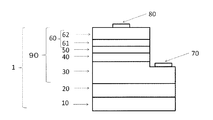
- FIG. 3 shows a typical example of a semiconductor chip obtained by the method of the present invention.
- the semiconductor wafer has a plurality of the semiconductor chip configurations shown in FIG. 3, and the layer configuration and the like are the same between the semiconductor wafer and the semiconductor chip.
- the semiconductor wafer 1 of the present invention is a semiconductor wafer having an element layer 90 including an n-type layer 30, an active layer 40, and a p-type layer 60 on one surface of a sapphire substrate 10.
- the element layer is characterized in that the surface is warped in a convex shape (FIG. 2).
- the semiconductor wafer of the present invention is characterized in that the surface of the element layer 90 is warped in a convex shape.
- the curvature indicating the degree of warpage is 530 km ⁇ 1 or more and 800 km ⁇ 1 or less.
- the curvature can be measured with an XRD (X-Ray Diffraction), a laser displacement meter, or an interference microscope.
- the curvature is a value measured with a laser displacement meter.
- the curvature is a value obtained from the surface of the element layer 90 in the semiconductor wafer before forming the electrode.
- the curvature of the outermost surface of the p-type layer 60 and when the p-type layer 60 has the p-type contact layer 62, it means the curvature of the surface. Moreover, when the curvature of a surface changes with measurement parts, the average value of the curvature in three or more measurement points is meant.
- the dislocation density of the element layer 90 is 1 ⁇ 10 8 to 1 ⁇ 10 9 [cm ⁇ 2 ].
- the dislocation density is a value measured with a transmission electron microscope, and is a value obtained by confirming the dislocation density of the n-type layer 30.
- the light output is not preferable.
- the reason for the excellent effect when the curvature of the convex surface of the element layer 90 is not less than 530 km ⁇ 1 and not more than 800 km ⁇ 1 is estimated by the present inventors as follows.
- the inventors of the present invention have grown an n-type AlGaN layer on the sapphire substrate 10 under various conditions. As a result, the (102) plane X-ray rocking curve is almost the same (from 700 to slightly over 800 [arcsec]; dislocation). Despite the fact that the density does not change.), It was found that the PL strength of the n-type AlGaN layer can be increased by increasing the curvature of the resulting laminate (n-type AlGaN layer surface) to some extent (See FIG. 1). From this result, it was considered that if it can be warped to some extent, it is suggested that in the active layer or the like, the incorporation of impurities and point defects is suppressed without increasing the dislocation density. The inventors have found that the light output can be efficiently increased by setting the curvature of the surface of the element layer 90 to 530 km ⁇ 1 or more and 800 km ⁇ 1 or less, and the present invention has been completed.
- the curvature of the surface of the element layer 90 when the curvature of the surface of the element layer 90 is less than 530 km ⁇ 1 , the effect of improving the light output is small, which is not preferable.
- the curvature is preferably 600 km ⁇ 1 or more and 800 km ⁇ 1 or less, and more preferably 600 km ⁇ 1 or more and 750 km ⁇ 1 or less.
- the sapphire substrate 10 is not particularly limited, and a known substrate manufactured by a known method can be used.
- the thickness of the sapphire substrate 10 is not particularly limited, and is usually 300 to 600 ⁇ m.
- the sapphire substrate 10 preferably has a (0001) plane as a growth plane (plane on which an element layer is grown).
- an element layer 90 is formed on a sapphire substrate 10.
- the composition of the element layer 90 is not particularly limited.
- the effect of the present invention is remarkably exhibited when the element layer 90 is composed of a group III nitride single crystal layer.
- the group III nitride single crystal layer particularly the AlxInyGazN layer having the above composition
- the group III nitride single crystal layer has a large difference in lattice constant from that of the sapphire substrate, and tends to cause dislocations.
- the light output tends to decrease.
- the present invention in such a conventional semiconductor wafer layer configuration in which dislocations occur at a high density and a decrease in output is observed, the light output can be increased without changing the layer configuration. Therefore, the present invention can exhibit an excellent effect when the element layer 90 contains Al.
- it is suitable for an ultraviolet light emitting diode (wafer) whose emission peak wavelength is in the ultraviolet region, specifically, in the range of 200 to 350 nm.
- the element layer 90 may be formed directly on the sapphire substrate 1, but it is preferable to form the element layer 90 after forming the buffer layer 20, as shown in FIG. Next, the buffer layer 20 will be described.
- the semiconductor wafer 1 of the present invention when used for an ultraviolet light emitting diode, it is preferable that 0.9 ⁇ X1 ⁇ 1, 0 ⁇ Y1 ⁇ 0.1, and 0 ⁇ Z1 ⁇ 0.1. Considering the characteristics, it is most preferable to employ the buffer layer 20 made of AlN.
- the thickness of the buffer layer 20 is not particularly limited, but is preferably 0.01 to 5 ⁇ m.
- the buffer layer 20 may be a single layer, but may be a plurality of layers of two or more layers as described in detail below.
- the plurality of layers may be layers having different compositions, or layers having the same composition but different growth conditions. For example, layers having the same composition but different growth conditions were grown by changing the ratio of the number of moles of nitrogen source gas to the number of moles of group III source gas (V / III ratio), which is one of the growth conditions. Refers to the layer. Most preferred is a layer of two or more layers made of AlN grown with varying V / III.
- the buffer layer 20 may be a graded layer whose composition changes continuously.
- the element layer 90 is preferably formed on the buffer layer 20. Next, each layer constituting the element layer 90 will be described.
- N-type layer 30 In the present invention, an n-type layer 30 is formed on the sapphire substrate 10 via the buffer layer 20 as necessary.
- the n-type layer 30 is a layer doped with an n-type dopant.
- the n-type layer 30 is not particularly limited.
- the n-type layer 30 is included in a range where the impurity concentration is 1 ⁇ 10 16 to 1 ⁇ 10 21 [cm ⁇ 3 ] using Si as a dopant.
- Layer 30 preferably exhibits n-type conductivity characteristics.
- the dopant material may be a material other than Si.
- the n-type layer 30 may be an inclined layer whose composition changes continuously.
- the thickness of the n-type layer 30 is preferably 0.1 to 20 ⁇ m.
- the active layer 40 is formed on the n-type layer 30.
- the active layer 40 may be composed of, for example, one or more well layers and barrier layers.
- the number of wells constituted by the well layers and the barrier layers may be one, or may be two or more. When there are a plurality, there is no particular limitation, but in consideration of the productivity of the nitride semiconductor light emitting device, it is preferably 10 or less.
- the layer in contact with the n-type layer 30 may be either a well layer or a barrier layer.
- the active layer 40 includes a barrier layer and a well layer.
- the barrier layer usually has a larger band gap than the well layer. That is, the barrier layer is formed of an AlGaInN layer having an Al composition ratio higher than that of the well layer.
- the AlGaInN layer preferably satisfies the composition represented by
- the thickness of the barrier layer 42 is preferably 2 to 50 nm.
- the well layer has a smaller band gap than the barrier layer. That is, the well layer is formed of an AlGaN single crystal having an Al composition ratio lower than that of the barrier layer.
- the thickness of the well layer 41 is preferably 1 to 20 nm.
- the p-type layer 60 may be formed directly on the active layer 40, but the p-type layer 60 is preferably formed via the electron blocking layer 50.
- the electron blocking layer 50 prevents a part of electrons injected from the n-type layer 30 to the active layer 40 due to application of an electric field from leaking to the p-type layer 60 side. Therefore, the electron block layer 50 can be substituted by a p-type cladding layer 60 described later.
- the Al composition of the p-type cladding layer is lowered and the film thickness is reduced. As a result, the driving voltage can be reduced.
- the band gap of the electron blocking layer 50 is the active layer 40 (the barrier layer having the maximum band gap in the active layer (the maximum Al composition)), and the p-type described in detail below.
- the band gap of the layer forming the layer 60 is preferably larger. Therefore, the electron block layer 40 is preferably formed from a single crystal made of AlInGaN having a higher Al composition ratio than these layers. That is, the electron blocking layer 50 is preferably formed from an AlGaN single crystal layer having a higher Al composition than any other layer.
- the electron block layer 50 is made of Al X5 In Y5 Ga Z5 N (X5, Y5, Z5 are rational numbers satisfying 0.7 ⁇ X5 ⁇ 1, 0 ⁇ Y5 ⁇ 0.3, and 0 ⁇ Z5 ⁇ 0.3.
- X5 + Y5 + Z5 1.0)
- the electron block layer 50 may be an inclined layer whose composition changes continuously.
- the electron blocking layer 50 may be an undoped layer or a p-type layer.
- the impurity concentration is 1 ⁇ 10 16 to 1 ⁇ 10 21 [cm ⁇ 3 ] with a dopant of p-type, for example, Mg as a dopant.
- the thickness of the electron block layer 50 is preferably 1 to 50 nm.
- the p-type layer 60 is formed on the active layer 40 or the electron blocking layer 50 provided as necessary.
- the p-type layer 60 is not particularly limited, but preferably includes a p-type cladding layer 61 and a p-type contact layer 62 on which a p-electrode 80 is formed.
- the p-type cladding layer 61 is preferably included, for example, in the range where the impurity concentration is 1 ⁇ 10 16 to 1 ⁇ 10 21 [cm ⁇ 3 ] using Mg as a dopant.
- the thickness of the p-type cladding layer 61 is not particularly limited, but is preferably 1 nm or more and 1 ⁇ m or less.
- P-type contact layer 62 In the present invention, it is preferable to provide a p-type contact layer 62 in contact with the p-electrode on the p-type cladding layer 61. By forming the p-type contact layer 62, it is easy to realize ohmic contact with the p-electrode 80, and it is possible to easily reduce the contact resistance.
- the p-type contact layer 62 is formed of a single crystal made of GaN.
- Mg is used as a dopant and the impurity concentration is 1 ⁇ 10 16 to 1 ⁇ 10 21 [cm ⁇ 3 ].
- the thickness of the p-type contact layer 62 is not particularly limited, but is preferably 1 nm or more and 1000 nm or less.
- the n electrode 70 is formed on the exposed surface of the n-type layer 30.
- Various materials can be used for the n-electrode 70, but a known material can be selected.
- Ti, Al, Rh, Cr, V, In, Ni, Pt, Au, or the like can be used. Of these, Ti, Al, Rh, Cr, V, Ni, and Au are preferably used.
- These negative electrodes may be a single layer having a layer containing an alloy or an oxide of these metals, or a multilayer structure, and a preferable combination from the viewpoint of ohmic properties and reflectivity is Ti / Al / Au.
- the thickness is not particularly limited, but is preferably 2 nm or more in view of production stability, and the upper limit is 2 ⁇ m.
- the p electrode 80 is formed on the p-type contact layer 62.
- This p-electrode 80 is preferably one having high transparency to ultraviolet light.
- the transmittance is 60% or more, preferably 70% or more, with respect to 265 nm light.
- the upper limit is preferably 100%, and industrially preferably 90% or more.
- the metal material used for the p-electrode 80 can be selected from known materials, though various examples are available. For example, Ni, Cr, Au, Mg, Zn, and Pd can be used.
- the translucent positive electrode may be a single layer having a layer containing an alloy or oxide of these metals, or a multilayer structure. A preferable combination is Ni / Au.
- the p electrode 80 When the p electrode 80 needs to have translucency, the smaller the film thickness, the better. Specifically, it is 10 nm or less, more preferably 5 nm or less, and the lower limit is 0.5 nm. In the case where the p-electrode 80 does not need to have translucency, this is not the only case, and the film thickness may be thick. Specifically, it is 500 nm or less, more preferably 100 nm or less, and the lower limit is 0.5 nm.
- a semiconductor light-emitting device having an n-electrode and a p-electrode on a semiconductor wafer is used, and a semiconductor chip is obtained by cutting the semiconductor light-emitting device.
- the suitable manufacturing method of the semiconductor wafer 1 of this invention is demonstrated.
- the element layer 90 is formed on the sapphire substrate 10 to manufacture the semiconductor wafer 1.
- the element layer is preferably grown on the (0001) plane.
- the (0001) plane may have an off angle, and it is preferable to form an element layer on the (0001) plane inclined at 0 to 5 °. Furthermore, it is preferable to incline in the m axis direction.
- the (0001) plane is preferably smooth, and it is preferable to use one having a surface roughness of about 0.2 nm or less.
- the curvature amount (curvature radius) of the sapphire substrate 10 before the element layer 90 is grown is 10 m or more.
- the upper limit of the radius of curvature is not particularly limited.
- the element layer 90 is formed on the sapphire substrate 10.
- the conditions for producing the semiconductor wafer of the present invention are not particularly limited, but it is preferably grown by a metal organic chemical vapor deposition (MOCVD) method.
- MOCVD metal organic chemical vapor deposition
- the conditions immediately before the buffer layer or the element layer is grown on the sapphire substrate 10 are important. I understood that. Specifically, it is preferable to introduce a certain amount of oxygen into the MOCVD apparatus before growing the buffer layer or the element layer on the sapphire substrate 10. However, the amount of oxygen introduced cannot be generally limited because the optimum value varies depending on the capacity and shape of each device.
- oxygen air
- the sapphire substrate 10 is set in an MOCVD apparatus, and thermal cleaning or the like is performed by a known method to form the buffer layer 20 or the element layer 90.
- the reason why the effect can be obtained by introducing oxygen is not clear, but a small amount of remaining oxygen affects the growth of the first layer formed on the sapphire substrate 10, so that the finally obtained element layer 90 is convex. It is thought that it can be warped.
- the element layer 90 can be warped in a convex shape by carrying out under pressure while growing a buffer layer and an n-type layer provided as necessary. Specifically, it is preferable that the layer is grown on the sapphire substrate 10 under a pressure of 50 to 200 Torr. Although the reason for this is not clear, it is considered that the element layer 90 finally obtained can be warped in a convex shape by affecting the growth of the layer formed by applying pressure in the initial stage of growth. .
- the element layer 90 may be directly formed on the (0001) plane on the sapphire substrate 10, but as described above, first, it is preferable that the element layer 90 is interposed via the buffer layer 20. Next, the growth of the buffer layer 20 will be described.
- the buffer layer 20 when the buffer layer 20 is provided, the preferred composition is as described above. In the present invention, although not particularly limited, it is preferably grown by a metal organic chemical vapor deposition (MOCVD) method.
- MOCVD metal organic chemical vapor deposition
- the above-described oxygen introduction method and / or growth method under a pressure of 50 to 200 Torr is adopted, and the buffer layer 20 It is preferable to control the V / III ratio under these growth conditions. That is, it is preferable to control the ratio of the number of moles of nitrogen source gas to the number of moles of group III source gas (V / III ratio).
- the range of the V / III ratio in the production conditions is not particularly limited, but is preferably 50 to 10,000.
- the buffer layer 20 in at least two stages.
- the raw material gas flow rate is adjusted so that the V / III ratio is 2000 or more and 10,000 or less, and a first buffer layer made of AlN single crystal is formed. It is preferable to adjust the raw material gas flow rate so that the V / III ratio is 50 or more and less than 2000 on the layer, and further form an AlN single crystal layer.
- an AlN single crystal layer can be grown in multiple stages within a range where the V / III ratio is 50 or more and less than 2000.
- the buffer layer (second buffer layer) in two stages after the first growth step and the second growth step.
- the second buffer layer is thicker than the first buffer layer.
- the thickness of the first buffer layer is preferably 0.004 ⁇ m to 0.5 ⁇ m
- the thickness of the second buffer layer is preferably 0.006 ⁇ m to 4.5 ⁇ m.
- a nitrogen source gas for example, ammonia
- a group III source gas for example, trimethylaluminum gas, trimethylgallium gas, trimethylindium gas.
- Etc. may be supplied onto the sapphire substrate 10 at 1100 to 1300 ° C. under a flow of hydrogen or nitrogen gas so as to have a desired composition and thickness.
- the growth method of the n-type layer 30 is not particularly limited, and is preferably grown by MOCVD.
- the buffer layer 20 is not provided, the n-type layer 30 is directly stacked on the sapphire substrate 10.
- a condition for growing the n-type layer 30 a known method can be adopted.
- the growth conditions on the sapphire substrate 10 and the buffer layer 20 can be the same.
- the n-type layer 30 may be grown by supplying an n-type dopant in addition to Al, Ga source gas and ammonia.
- an n-type dopant element a known element such as Si or O can be used without limitation, but Si is preferably used from the viewpoint of ease of control.
- the Si source monosilane (SIH 4), or the like can be used tetraethyl silane (TESi).
- the growth temperature for growing the n-type layer 30 is not particularly limited, but is preferably 900 ° C. or higher and 1100 ° C. or lower.
- the growth rate is preferably 0.1 to 2.0 ⁇ m / h.
- the V / III ratio is not particularly limited, but is preferably 1500 to 10000, more preferably 2000 to 5000 in order to satisfy the growth rate in the temperature range.
- the active layer 40 can also be grown by MOCVD so as to satisfy a desired composition, like the buffer layer 20 and the n-type layer 30.
- a known method can be adopted as a condition for forming the active layer 40.
- the growth temperature of the active layer 40 is not particularly limited, but is preferably over 1000 ° C. and 1200 ° C. or less, preferably over 1020 ° C. and 1100 ° C. or less.
- the V / III ratio during growth of the active layer 40 is not particularly limited, but is preferably 1000 to 10,000, and more preferably 1500 to 8000.
- the growth rate during the growth of the active layer 40 is preferably 0.05 to 1.0 ⁇ m / h, more preferably 0.1 to 0.8 ⁇ m / h.
- the growth rate of this active layer is also preferably in the range of 0.05 to 1.0 ⁇ m / h for all of the quantum well layer and the barrier layer.
- the electron blocking layer 50 formed as necessary can also be grown by MOCVD.
- MOCVD Metal Organic Chemical Vapor deposition
- the growth temperature of the electron blocking layer 50 is not particularly limited, but preferably exceeds 1020 ° C. and is 1200 ° C. or less, more preferably exceeds 1050 ° C. and is 1150 ° C. or less.
- the growth rate is preferably 0.1 ⁇ m to 1.0 ⁇ m / h, more preferably 0.1 to 0.8 ⁇ m / h.
- the V / III ratio is not particularly limited, but is preferably in the range of 2000 to 20000, and more preferably in the range of 2500 to 15000.
- the electron blocking layer 50 can be made p-type by adding p-type impurities.
- the electron block layer 50 is manufactured by supplying p-type impurities in addition to Al and Ga source gases and ammonia.
- p-type impurity a known material can be used without limitation, but it is preferable to use Mg in consideration of the activation energy of the p-type impurity.
- the p-type cladding layer 61 can also be grown by the MOCVD method. Specifically, it is manufactured by supplying p-type impurities in addition to Al and Ga source gases and ammonia.
- the p-type impurity a known material can be used without limitation, but it is preferable to use Mg in consideration of the activation energy of the p-type impurity.
- a known method can be adopted.
- the growth temperature, the growth rate, and the V / III ratio it is preferable to adopt the conditions described for the electron block layer 50.
- the p-type contact layer 62 can be grown by the MOCVD method, and the same impurities as the p-type cladding layer 61 can be added.
- the growth temperature is not particularly limited, but is preferably 1000 ° C. or higher and 1080 ° C. or lower, and more preferably 1020 ° C. or higher and 1050 ° C. or lower.
- the growth rate is not particularly limited, but is preferably 0.03 to 1.0 ⁇ m / h.
- the V / III ratio is preferably set in the range of 2000 to 15000, more preferably 4000 to 12000, and most preferably 6000 to 10,000.
- the n-electrode 70 is formed on the exposed surface of the n-type layer 30.
- the exposed surface of the n-type layer 30 is formed by means such as etching.
- etching As an etching method, dry etching such as reactive ion etching and inductively coupled plasma etching is preferably used.
- a surface treatment with an acid or alkali solution in order to remove etching damage.
- the patterning of the n-electrode can be performed using a lift-off method.
- examples of the method for depositing the metal for forming the n-electrode include vacuum deposition, sputtering, and chemical vapor deposition, but vacuum deposition is preferable in order to eliminate impurities in the electrode metal.
- the material used for the n-electrode is as described above.
- the p-electrode 80 is preferably patterned by a lift-off method.
- the metal material used for the p-electrode 80 is as described above. Examples of the method for depositing the metal of the p-electrode 80 include vacuum deposition, sputtering, chemical vapor deposition, and the like, but vacuum deposition is preferred in order to eliminate impurities in the electrode metal.
- Example 1 A sapphire C-plane ((0001) plane) single crystal substrate ( ⁇ 2 inch ⁇ thickness 330 ⁇ m) was used as the crystal growth substrate. 5 minutes after opening the MOCVD apparatus, the sapphire substrate was placed on a susceptor in the MOCVD apparatus, and then the sapphire substrate was heated to 1230 ° C. and kept for 10 minutes while flowing hydrogen at a flow rate of 13 slm (heat treatment step). ).
- buffer layer 20 (Formation of buffer layer 20) Next, the temperature of the sapphire substrate is set to 1180 ° C., the trimethylaluminum flow rate is set to 13.1 ⁇ mol / min, the ammonia flow rate is set to 1 slm, and the raw material gas flow rate is adjusted so that the V / III ratio at this time is 3400. Then, an AlN single crystal layer having a thickness of 0.1 ⁇ m was formed as a first buffer layer under a pressure of 25 Torr (first growth step; growth of first buffer layer).
- the temperature of the substrate in which the AlN single crystal layer of the first buffer layer is laminated on the sapphire substrate is 1180 ° C.
- the trimethylaluminum flow rate is 26 ⁇ mol / min
- the ammonia flow rate is 0.5 slm
- the V / III ratio at this time
- the raw material gas flow rate was adjusted so as to be 850, and an AlN single crystal layer was formed as a second buffer layer at a total flow rate of 10 slm and a pressure of 25 Torr (second growth step; second buffer layer growth).
- n-type layer 30 (Formation of n-type layer 30) Next, the substrate temperature was set to 1050 ° C., the trimethylaluminum flow rate was 35 ⁇ mol / min, the trimethylgallium flow rate was 18 ⁇ mol / min, the tetraethylsilane flow rate was 0.02 ⁇ mol / min, and the ammonia flow rate was 1.5 slm.
- An n-type layer 30 having a Ga composition of 30% and an In composition of 0% was formed to 2.0 ⁇ m. During this time, the pressure in the apparatus was 38 Torr. At this time, the half width of the X-ray rocking curve was (102) plane: 700 arcsec.
- an Al 0.5 Ga 0.5 N well layer was formed in a thickness of 2 nm under the same conditions as those for growing the n-type layer except that the flow rate of trimethylgallium was 40 ⁇ mol / min and that of trimethylaluminum was 2 ⁇ mol / min.
- a triple quantum well layer was formed by repeating the growth of the well layer and the barrier layer three times. During this time, the pressure in the apparatus was 38 Torr.
- the p-type cladding layer 61 was formed to have a thickness of 35 nm under the same conditions as those for the growth of the n-type layer, except that bicyclopentadienyl magnesium was supplied at 1.0 ⁇ mol / min with the substrate temperature fixed.
- the Al composition was 70%
- the Ga composition was 30%
- the In composition was 0%.
- the pressure in the apparatus was 38 Torr.
- the curvature of the surface of the element layer 90 (p-type contact layer 62) of the obtained semiconductor wafer was measured by a laser displacement meter method.
- the curvature of the semiconductor wafer was 543 km ⁇ 1 and the results are shown in Table 1.
- n-electrode 70 The obtained semiconductor wafer was heat-treated at 900 ° C. for 20 minutes in a nitrogen atmosphere. Thereafter, a predetermined resist pattern was formed on the surface of the p-type contact layer 62 by photolithography, and a window portion where no resist pattern was formed was etched by reactive ion etching until the surface of the n-type layer 30 was exposed. Thereafter, a Ti (20 nm) / Al (200 nm) / Au (5 nm) electrode (negative electrode) is formed as an n electrode 70 on the surface of the n-type layer 30 by a vacuum deposition method, and in a nitrogen atmosphere, 810 ° C. for 1 minute. The heat treatment was performed under the following conditions.
- the obtained semiconductor light emitting device had a light output and a wavelength of 0.44 mW and 272 nm at a driving current of 30 mA.
- the results are summarized in Table 1.
- Example 2 In Example 1, the semiconductor wafer and the semiconductor light emitting device were all under the same conditions except that the trimethylaluminum flow rate in the buffer layer 20 (first growth step) was 13.1 ⁇ mol / min and the V / III ratio was 5100. Was made.
- the optical output and wavelength at a driving current of 30 mA were 0.87 mW, 269 nm, and the curvature of the semiconductor wafer was 613 km ⁇ 1 . The results are shown in Table 1.
- Example 3 In Example 1, the semiconductor wafer and the semiconductor light emitting device were all manufactured under the same conditions except that the trimethylaluminum flow rate in the buffer layer 20 (first growth step) was 6.6 ⁇ mol / min and the V / III ratio was 6800. Produced. When the same evaluation as in Example 1 was performed, the optical output and wavelength at a driving current of 30 mA were 1.48 mW, 267 nm, and the curvature of the semiconductor wafer was 701 km ⁇ 1 . The results are shown in Table 1.
- Comparative Example 1 Formation of buffer layer 20
- the opening time before introducing the sapphire substrate into the MOCVD apparatus was 1 minute, and the buffer layer 20 was grown by 2 ⁇ m under the same conditions as in the second growth step except that the first growth step was not performed.
- the growth conditions after the n-type layer 30 were the same as in Example 1, and a semiconductor wafer and a semiconductor light emitting device were produced. In addition, the half width (102) plane of the X-ray rocking curve when the n-type layer was formed under these conditions was measured.
- the obtained semiconductor light emitting device had an optical output and a wavelength of 0.32 mW and 260 nm at a driving current of 30 mA, and the curvature of the semiconductor wafer was 507 km ⁇ 1 .
- Table 1 summarizes the results.
Landscapes
- Led Devices (AREA)
- Crystals, And After-Treatments Of Crystals (AREA)
- Chemical & Material Sciences (AREA)
- Crystallography & Structural Chemistry (AREA)
Abstract
Description
本発明の半導体ウェハ1は、サファイア基板10の一方の面上に、n型層30、活性層40、及びp型層60を含む素子層90を有する半導体ウェハである。そして、該素子層を表面が凸状に反っていることを特徴とする(図2)。
本発明の半導体ウェハは、該素子層90の表面が凸状に反っていることを特徴とする。そして、その反りの度合いを示す曲率が530km-1以上800km-1以下であることを特徴とする。なお、曲率は、XRD(X-Ray Diffraction)、レーザー変位計、干渉顕微鏡により測定できる。本発明において、曲率は、レーザー変位計で測定した値である。なお、該曲率は、電極を形成する前の半導体ウェハにおける素子層90の表面から求めた値である。すなわち、p型層60の最表面の曲率を意味し、p型層60がp型コンタクト層62を有する場合には、その表面の曲率をいう。また、表面の曲率が測定部位により異なる場合には、3点以上の測定点における曲率の平均値を意味する。
(サファイア基板)
サファイア基板10は、特に制限されるものではなく、公知の方法で製造された、公知の基板を用いることができる。該サファイア基板10の厚みは、特に制限されるものではなく、通常、300~600μmである。
本発明の半導体ウェハ1は、サファイア基板10上に、素子層90が形成される。素子層90の組成は、特に制限されるものではない。中でも、本発明の効果が顕著に発揮されるのは、該素子層90が、III族窒化物単結晶層から構成される場合であり、その中でも、AlxInyGazN(x、y、zは、0.3≦x≦1.0、0≦y≦0.7、0≦z≦0.7を満たす有理数であり、x+y+z=1.0である)で示される組成を満足するAlGaInN層で構成される場合である。その理由は、III族窒化物単結晶層、特に、前記組成のAlxInyGazN層は、特に、サファイア基板と格子定数の差が大きく、転位が入り易く、その結果、光出力が低下し易い傾向にある。本発明は、このような従来では高密度に転位が生じ、出力の低下がみられる半導体ウェハの層構成において、層構成を変更させることなく、光出力を高めることができる。そのため、本発明は、素子層90がAlを含む場合に優れた効果を発揮することができる。具体的には、発光ピーク波長が、紫外領域、具体的には、200~350nmの範囲にある紫外発光ダイオード(ウェハ)に適している。
本発明において、バッファ層を設ける場合、バッファ層20は、III族窒化物単結晶層からなることが好ましく、AlX1InY1GaZ1N(X1、Y1、Z1は、0.8≦X1≦1、0≦Y1≦0.2、0≦Z1≦0.2を満たす有理数であり、X1+Y1+Z1=1.0である)で示される組成を満足するAlGaInN層であることが好ましい。この中でも、本発明の半導体ウェハ1を紫外発光ダイオードに使用する場合には、0.9≦X1≦1、0≦Y1≦0.1、0≦Z1≦0.1であることが好ましく、生産性を考慮すると、AlNからなるバッファ層20を採用することが最も好ましい。
本発明において、サファイア基板10上には、必要に応じて前記バッファ層20を介して、n型層30を形成する。このn型層30とは、n型のドーパントがドープされている層である。このn型層30は、特に制限されるものではないが、例えば、Siをドーパントとして不純物濃度が1×10¹⁶~1×10²¹[cm-3]となる範囲で含まれることにより、n型層30がn型の導電特性を示すことが好ましい。ドーパント材料は、Si以外の材料であってもよい。
活性層40は、前記n型層30の上に形成される。活性層40は、例えば、1層以上の井戸層と障壁層により構成されればよい。井戸層と障壁層より構成される井戸数は、1つであってもよいし、2つ以上の複数であってもよい。複数ある場合には、特に制限されるものではないが、窒化物半導体発光素子の生産性を考慮すると、10以下であることが好ましい。また、n型層30と接する層は、井戸層、および障壁層の何れであってもよい。
活性層40は、障壁層と井戸層とからなる。そして、障壁層は、通常、井戸層よりもバンドギャップが大きくなる。つまり、障壁層は、井戸層よりも高いAl組成比のAlGaInN層で形成される。前記の通り、本発明の半導体ウェハは、紫外発光ダイオードに好適に適用できる。そのため、障壁層は、AlX3InY3GaZ3N(X3、Y3、Z3は、0.3≦X3≦1.0、0≦Y3≦0.7、0≦Z3≦0.7を満たす有理数であり、X3+Y3+Z3=1.0である)で示される組成を満足するAlGaInN層からなることが好ましい。また、障壁層42の厚みは、2~50nmであることが好ましい。
井戸層は、障壁層よりもバンドギャップが小さくなる。つまり、井戸層は、障壁層よりも低いAl組成比となるAlGaNの単結晶から形成される。前記の通り、本発明の半導体ウェハは、紫外発光ダイオードに好適に適用できる。そのため、井戸層は、AlX4InY4GaZ3N(X4、Y4、Z4は、0.1≦X4≦0.9、0.1≦Y4≦0.8、0≦Z4≦0.8を満たす有理数であり、X4+Y4+Z4=1.0である。ただし、X3>X4でありかつZ3≦Z4である。)で示される組成を満足するAlGaInN層からなることが好ましい。また、井戸層41の厚みは、1~20nmであることが好ましい。
本発明においては、前記活性層40の上に、直接、p型層60が形成されてもよいが、電子ブロック層50を介して、p型層60が形成されることが好ましい。電子ブロック層50は、電界をかけたことによりn型層30から活性層40へと注入された電子の一部がp型層60側に漏れることを抑制する。そのため、電子ブロック層50は後述するp型クラッド層60で代用することも可能であるが、電子ブロック層50を設けることにより、p型クラッド層のAl組成を下げる、かつ膜厚を薄くとすることができ、その結果、駆動電圧を低減できるという効果が得られる。
本発明においては、前記活性層40、又は必要の応じて設けられる電子ブロック層50上に、p型層60を形成する。このp型層60は、特に制限されるものではないが、p型クラッド層61、およびその上にp電極80が形成されるp型コンタクト層62からなることが好ましい。
本発明の半導体ウェハ1は、前記の通り、200~350nmの範囲にある紫外発光ダイオードに好適に適用できる。そのため、p型クラッド層61は、AlX6InY6GaZ6N(X6、Y6、Z6は、0.3≦X6≦1.0、0≦Y6≦0.7、0≦Z6≦0.7を満たす有理数とし、X6+Y6+Z6=1.0である)で示される組成を満足するAlInGaN層からなることが好ましい。
本発明においては、前記p型クラッド層61上に、p電極と接するp型コンタクト層62を設けることが好ましい。p型コンタクト層62を形成することにより、p電極80とのオーミック接触を実現し易くするとともに、その接触抵抗の低減を実現し易くすることができる。
n電極70は、n型層30の露出面に形成される。n電極70に用いられる材料は、様々挙げられるが公知の材料から選択することができる。たとえば、Ti、Al、Rh、Cr、V、In、Ni、及びPt、Auなどを用いる事ができる。中でも、Ti、Al、Rh、Cr、V、Ni、Auを使用することが好ましい。これら負電極は、これらの金属の合金または酸化物を含む層を有する単層、又は多層構造であってもよく、オーミック性および反射率の観点から好ましい組み合わせは、Ti/Al/Auである。厚みは、特に制限されるものではないが、生産の安定性を考えると2nm以上が好ましく、上限は2μmである。
p電極80は、p型コンタクト層62上に形成される。このp電極80は、紫外光に対して高い透過性を有するものであることが好ましい。具体的には、265nmの光に対して透過率60%以上、好適には70%以上である。特に制限されるものではないが、上限は100%であることが好ましく、工業的には90%以上であることが好ましい。
(サファイア基板の準備)
本発明においては、サファイア基板10上に素子層90を形成して半導体ウェハ1を製造する。使用するサファイア基板10は、(0001)面上に前記素子層を成長させることが好ましい。この(0001)面は、オフ角を有していてもよく、0~5°に傾斜している(0001)面上に素子層を形成することが好ましい。さらにm軸方向に傾いていることが好ましい。
本発明において、バッファ層20を設ける場合、好ましい組成は前記の通りである。本発明においては、特に制限されるものではないが、有機金属気相成長(MOCVD)法で成長することが好ましい。
n型層30の成長方法も、特に制限されるものではなく、MOCVD法で成長することが好ましい。バッファ層20を設けない場合には、サファイア基板10上には、このn型層30が直接積層される。n型層30を成長する条件は、公知の方法を採用することができる。サファイア基板10上、バッファ層20上の成長条件は同じ条件とすることができる。
次いで、活性層40も、前記バッファ層20、n型層30と同じく、所望の組成を満足するように、MOCVD法で成長することができる。活性層40を形成する条件は、公知の方法を採用することがでる。
必要に応じて形成される電子ブロック層50も、MOCVD法により成長させることができる。電子ブロック層50を形成する条件は、公知の方法を採用することができる。
(p型クラッド層61)
p型クラッド層61も、MOCVD法により成長させることができる。具体的には、AlおよびGa原料ガス、およびアンモニアに加えて、p型不純物を供給することにより製造される。p型不純物には、公知の材料を制限なく使用できるが、p型不純物の活性化エネルギーなどを勘案すると、Mgを使用することが好ましい。
p型コンタクト層62も同様に、MOCVD法により成長させることができ、p型クラッド層61と同じ不純物を添加することができる。
n電極70は、前記n型層30の露出面上に形成される。n型層30の露出面は、エッチング等の手段で形成される。エッチングの手法としては、好適には反応性イオンエッチング、誘導結合プラズマエッチング等のドライエッチングが挙げられる。前記n型層30の露出面を形成後、エッチングのダメージを除去するため、酸またはアルカリの溶液で表面処理を施すことが好ましい。また、n電極のパターンニングは、リフトオフ法を用いて実施することができる。
p電極80のパターニングは、リフトオフ法を用いることが好ましい。p電極80に用いられる金属材料は、前記の通りである。p電極80の金属を堆積する方法は、真空蒸着、スパッタリング、化学気相成長法等が挙げられるが、電極金属中の不純物を排除するため真空蒸着が好ましい。
結晶成長用基板にはサファイアC面((0001)面)単結晶基板(Φ2インチ×厚み330μm)を用いた。MOCVD装置を開放して5分間後、該サファイア基板をMOCVD装置内のサセプタ上に設置した後、水素を13slmの流量で流しながら、サファイア基板を1230℃まで加熱し、10分間保持した(熱処理工程)。
次いで、サファイア基板の温度を1180℃とし、トリメチルアルミニウム流量を13.1μmol/min、アンモニア流量を1slmとして、この際のV/III比3400となるように原料ガス流量を調整し、全流量が10slm、圧力が25Torrの条件で第一バッファ層としてAlN単結晶層を厚さ0.1μm形成した(第一成長工程;第一バッファ層の成長)。
次いで、サファイア基板上に第一バッファ層のAlN単結晶層が積層された基板の温度を1180℃とし、トリメチルアルミニウム流量を26μmol/min、アンモニア流量を0.5slmとして、この際のV/III比が850となるように原料ガス流量を調整し、全流量が10slm、圧力が25Torrの条件で第二バッファ層としてAlN単結晶層を1.9μm形成した(第二成長工程;第二バッファ層の成長)。
次いで、基板温度を1050℃とし、トリメチルアルミニウム流量を35μmol/min、トリメチルガリウム流量を18μmol/min、テトラエチルシラン流量を0.02μmol/min、アンモニア流量を1.5slmの条件で、Al組成70%、Ga組成30%、In組成0%のn型層30を2.0μm形成した。この間装置内の圧力は38Torrとした。このときX線ロッキングカーブの半値幅は(102)面:700arcsecであった。
次いで、基板温度を1060℃に設定し、温度が一定となった後、テトラエチルシラン流量を0.002μmol/min、トリメチルアルミニウム流量を13.3μmol/min、トリメチルガリウム流量を11.2μmol/min、とした以外は、前記n型層の成長条件と同条件でAl0.7Ga0.3N障壁層を7nm形成した。
次いで、トリメチルガリウム流量を40μmol/min、トリメチルアルミニウムを2μmol/minとした以外は、前記n型層を成長する条件と同条件でAl0.5Ga0.5N井戸層を2nm形成した。この井戸層と障壁層の成長を3回繰り返すことにより3重量子井戸層を形成した。この間装置内の圧力は38Torrとした。
次いで、トリメチルガリウムおよびテトラエチルシランの供給を停止し、基板温度を1100℃に設定した。温度が一定になった後、ビシシクロペンタジエニルマグネシウムを1.0μmol/minで供給した以外は、前記n型層の成長条件と同条件で電子ブロック層50を20nm形成した。このときAl組成は100%である。この間装置内の圧力は38Torrとした。
(p型クラッド層61の形成)
次いで、基板温度を固定したままビシシクロペンタジエニルマグネシウムを1.0μmol/minで供給した以外は、前記n型層の成長条件と同条件でp型クラッド層61を35nm形成した。このとき、Al組成70%、Ga組成30%、In組成0%であった。この間装置内の圧力は38Torrとした。
次いで、基板温度を1030℃、圧力を150Torrに変更した後、トリメチルガリウム流量が36.0μmol/min、アンモニア流量が2.5slm、ビシシクロペンタジエニルマグネシウム流量が0.66μmol/min、キャリアガス流量(水素)が3.5slmの条件で、p型コンタクト層62としてGaN層を240nm形成した。この間装置内の圧力は150Torrとした。このようにして半導体ウェハを製造した。
得られた半導体ウェハを窒素雰囲気中、20分間、900℃の条件で熱処理を行った。その後、p型コンタクト層62の表面にフォトリソグラフィーにより所定のレジストパターンを形成し、レジストパターンの形成されていない窓部を反応性イオンエッチングによりn型層30の表面が露出するまでエッチングした。その後、n型層30の表面に真空蒸着法によりn電極70として、Ti(20nm)/Al(200nm)/Au(5nm)電極(負電極)を形成し、窒素雰囲気中、1分間、810℃の条件で熱処理を行った。
次いで、p型コンタクト層62の表面に、真空蒸着法によりp電極80として、Ni(20nm)/Au(50nm)電極(正電極)を形成した後、酸素雰囲気中、3分間、550℃の条件で熱処理を行い、窒化物半導体発光素子を作製した。
実施例1においてバッファ層20における(第一成長工程)のトリメチルアルミニウム流量を13.1μmol/minとし、この際のV/III比を5100とした以外は全て同じ条件にて半導体ウェハ、半導体発光素子を作製した。実施例1と同様の評価を行ったところ、駆動電流30mAにおける光出力および波長は0.87mW、269nmであり、半導体ウェハの曲率は613km-1であった。結果を表1に示した。
実施例1においてバッファ層20における(第一成長工程)のトリメチルアルミニウム流量を6.6μmol/minとしこの際のV/III比を6800とした以外は全て同じ条件にて半導体ウェハ、半導体発光素子を作製した。実施例1と同様の評価を行ったところ、駆動電流30mAにおける光出力および波長は1.48mW、267nmであり、半導体ウェハの曲率は701km-1であった。結果を表1に示した。
(バッファ層20の形成)
実施例1において、サファイア基板をMOCVD装置に導入する前の開放時間を1分間とし、第一成長工程を実施しなかった以外は第二成長工程と同じ条件でバッファ層20を2μm成長した。
n型層30以降の成長条件等は、実施例1と同様の操作を行い、半導体ウェハ、半導体発光素子を作製した。また、この条件でn型層を形成した際のX線ロッキングカーブの半値幅(102)面を測定した。

10 サファイア基板
20 バッファ層
30 n型層
40 活性層
50 電子ブロック層
60 p型層
61 p型クラッド層
62 p型コンタクト層
70 n電極
80 p電極
Claims (8)
- サファイア基板の一方の面上に、n型層、活性層、及びp型層を含む素子層を有する半導体ウェハであって、
該素子層の表面が凸状に反っており、その曲率が530km-1以上800km-1以下であることを特徴とする半導体ウェハ。 - 前記サファイア基板の素子層を有する面が(0001)面であることを特徴とする請求項1に記載の半導体ウェハ。
- 前記素子層が、III族窒化物単結晶層からなることを特徴とする請求項1に記載の半導体ウェハ。
- 前記III族窒化物単結晶層が、AlxInyGazN(x、y、zは、0.3≦x≦1.0、0≦y≦0.7、0≦z≦0.7を満たす有理数であり、x+y+z=1.0である)で示される組成を満足するAlGaInN層からなることを特徴とする請求項3に記載の半導体ウェハ。
- 前記サファイア基板の一方の面上と素子層との間に、AlxInyGazN(x、y、zは、0.8≦x≦1.0、0≦y≦0.2、0≦z≦0.2を満たす有理数であり、x+y+z=1.0である)からなるバッファ層を有することを特徴とする請求項1に記載の半導体ウェハ。
- 前記バッファ層が第一バッファ層、及び第二バッファ層の2層を少なくとも有することを特徴とする請求項5に記載の半導体ウェハ。
- 請求項1~6の何れかに記載の半導体ウェハのn型層上にn電極を有し、p型層上にp電極を有することを特徴とする素子回路付半導体ウェハ。
- 請求項1~6の何れかに記載の半導体ウェハを切断して半導体チップとする工程を含む半導体発光素子の製造方法。
Priority Applications (5)
| Application Number | Priority Date | Filing Date | Title |
|---|---|---|---|
| CN201780021775.9A CN109075224B (zh) | 2016-04-08 | 2017-04-07 | 半导体晶片 |
| KR1020187028964A KR102112249B1 (ko) | 2016-04-08 | 2017-04-07 | 반도체 웨이퍼 |
| JP2018510677A JP6830098B2 (ja) | 2016-04-08 | 2017-04-07 | 半導体ウェハ |
| US16/092,007 US10770621B2 (en) | 2016-04-08 | 2017-04-07 | Semiconductor wafer |
| EP17779237.1A EP3442038B1 (en) | 2016-04-08 | 2017-04-07 | Semiconductor wafer |
Applications Claiming Priority (2)
| Application Number | Priority Date | Filing Date | Title |
|---|---|---|---|
| JP2016077829 | 2016-04-08 | ||
| JP2016-077829 | 2016-04-08 |
Publications (1)
| Publication Number | Publication Date |
|---|---|
| WO2017175860A1 true WO2017175860A1 (ja) | 2017-10-12 |
Family
ID=60001174
Family Applications (1)
| Application Number | Title | Priority Date | Filing Date |
|---|---|---|---|
| PCT/JP2017/014519 Ceased WO2017175860A1 (ja) | 2016-04-08 | 2017-04-07 | 半導体ウェハ |
Country Status (6)
| Country | Link |
|---|---|
| US (1) | US10770621B2 (ja) |
| EP (1) | EP3442038B1 (ja) |
| JP (1) | JP6830098B2 (ja) |
| KR (1) | KR102112249B1 (ja) |
| CN (1) | CN109075224B (ja) |
| WO (1) | WO2017175860A1 (ja) |
Cited By (5)
| Publication number | Priority date | Publication date | Assignee | Title |
|---|---|---|---|---|
| JP2019110195A (ja) * | 2017-12-18 | 2019-07-04 | 旭化成株式会社 | 窒化物半導体発光素子 |
| JP2021174876A (ja) * | 2020-04-24 | 2021-11-01 | 日機装株式会社 | 半導体発光素子および半導体発光素子の製造方法 |
| JP2022553236A (ja) * | 2019-10-17 | 2022-12-22 | コミッサリア ア レネルジー アトミーク エ オ ゼネルジ ザルタナテイヴ | マグネシウム原子でPドープされたAlNに基づく半導体及びドープされたダイヤモンドの層を含む発光ダイオード |
| US11637221B2 (en) | 2017-11-09 | 2023-04-25 | Asahi Kasei Kabushiki Kaisha | Nitride semiconductor element, nitride semiconductor light emitting element, ultraviolet light emitting element |
| JP2023108178A (ja) * | 2022-01-25 | 2023-08-04 | 日機装株式会社 | 窒化物半導体発光素子の製造方法 |
Families Citing this family (3)
| Publication number | Priority date | Publication date | Assignee | Title |
|---|---|---|---|---|
| KR102315911B1 (ko) * | 2020-01-08 | 2021-10-22 | 웨이브로드 주식회사 | 반도체 발광소자 및 이를 제조하는 방법 |
| EP4292123A4 (en) * | 2021-02-26 | 2025-03-05 | The Regents of University of California | Method to improve performances of tunnel junctions grown by metal organic chemical vapor deposition |
| JP2024058791A (ja) | 2022-10-17 | 2024-04-30 | スタンレー電気株式会社 | 垂直共振器型発光素子 |
Citations (4)
| Publication number | Priority date | Publication date | Assignee | Title |
|---|---|---|---|---|
| JP2000349338A (ja) * | 1998-09-30 | 2000-12-15 | Nec Corp | GaN結晶膜、III族元素窒化物半導体ウェーハ及びその製造方法 |
| JP2002222772A (ja) * | 2001-01-29 | 2002-08-09 | Matsushita Electric Ind Co Ltd | 窒化物半導体基板の製造方法 |
| US20050167683A1 (en) * | 2004-01-29 | 2005-08-04 | Lee Chang H. | Sapphire/gallium nitride laminate having reduced bending deformation |
| WO2005099057A1 (ja) * | 2004-03-31 | 2005-10-20 | Nec Corporation | 窒化物半導体発光素子用ウエハとその製造方法およびそのウエハから得られた窒化物半導体発光素子 |
Family Cites Families (14)
| Publication number | Priority date | Publication date | Assignee | Title |
|---|---|---|---|---|
| US6252261B1 (en) | 1998-09-30 | 2001-06-26 | Nec Corporation | GaN crystal film, a group III element nitride semiconductor wafer and a manufacturing process therefor |
| US6946788B2 (en) * | 2001-05-29 | 2005-09-20 | Toyoda Gosei Co., Ltd. | Light-emitting element |
| JP2003063897A (ja) * | 2001-08-28 | 2003-03-05 | Sony Corp | 窒化物系iii−v族化合物半導体基板およびその製造方法ならびに半導体発光素子の製造方法ならびに半導体装置の製造方法 |
| JP2005116785A (ja) | 2003-10-08 | 2005-04-28 | Nippon Telegr & Teleph Corp <Ntt> | 半導体材料薄膜の成長法 |
| WO2011065745A2 (ko) * | 2009-11-27 | 2011-06-03 | 서울옵토디바이스주식회사 | 발광다이오드 패키지 |
| CN102792420B (zh) * | 2010-03-05 | 2016-05-04 | 并木精密宝石株式会社 | 单晶衬底、单晶衬底的制造方法、带多层膜的单晶衬底的制造方法以及元件制造方法 |
| JP2012009695A (ja) * | 2010-06-25 | 2012-01-12 | Showa Denko Kk | 半導体発光素子の製造方法、半導体発光素子、電子機器及び機械装置 |
| WO2012150647A1 (ja) * | 2011-05-02 | 2012-11-08 | パナソニック株式会社 | スーパールミネッセントダイオード |
| CN106968014B (zh) | 2012-03-21 | 2019-06-04 | 弗赖贝格化合物原料有限公司 | 用于制备iii-n单晶的方法以及iii-n单晶 |
| KR20130107791A (ko) * | 2012-03-23 | 2013-10-02 | 엘지이노텍 주식회사 | 발광소자 |
| JP6024533B2 (ja) * | 2012-03-28 | 2016-11-16 | 日亜化学工業株式会社 | サファイア基板及びその製造方法並びに窒化物半導体発光素子 |
| US20160265140A1 (en) * | 2012-10-31 | 2016-09-15 | Namiki Seimitsu Houseki Kabushiki Kaisha | Single crystal substrate, manufacturing method for single crystal substrate, manufacturing method for single crystal substrate with multilayer film, and element manufacturing method |
| CN105102695B (zh) * | 2013-12-18 | 2018-06-12 | 日本碍子株式会社 | 复合基板和功能元件 |
| CN105448852A (zh) * | 2014-08-27 | 2016-03-30 | 群创光电股份有限公司 | 曲面电子装置 |
-
2017
- 2017-04-07 KR KR1020187028964A patent/KR102112249B1/ko active Active
- 2017-04-07 US US16/092,007 patent/US10770621B2/en active Active
- 2017-04-07 WO PCT/JP2017/014519 patent/WO2017175860A1/ja not_active Ceased
- 2017-04-07 CN CN201780021775.9A patent/CN109075224B/zh active Active
- 2017-04-07 JP JP2018510677A patent/JP6830098B2/ja active Active
- 2017-04-07 EP EP17779237.1A patent/EP3442038B1/en active Active
Patent Citations (4)
| Publication number | Priority date | Publication date | Assignee | Title |
|---|---|---|---|---|
| JP2000349338A (ja) * | 1998-09-30 | 2000-12-15 | Nec Corp | GaN結晶膜、III族元素窒化物半導体ウェーハ及びその製造方法 |
| JP2002222772A (ja) * | 2001-01-29 | 2002-08-09 | Matsushita Electric Ind Co Ltd | 窒化物半導体基板の製造方法 |
| US20050167683A1 (en) * | 2004-01-29 | 2005-08-04 | Lee Chang H. | Sapphire/gallium nitride laminate having reduced bending deformation |
| WO2005099057A1 (ja) * | 2004-03-31 | 2005-10-20 | Nec Corporation | 窒化物半導体発光素子用ウエハとその製造方法およびそのウエハから得られた窒化物半導体発光素子 |
Non-Patent Citations (1)
| Title |
|---|
| See also references of EP3442038A4 * |
Cited By (7)
| Publication number | Priority date | Publication date | Assignee | Title |
|---|---|---|---|---|
| US11637221B2 (en) | 2017-11-09 | 2023-04-25 | Asahi Kasei Kabushiki Kaisha | Nitride semiconductor element, nitride semiconductor light emitting element, ultraviolet light emitting element |
| JP2019110195A (ja) * | 2017-12-18 | 2019-07-04 | 旭化成株式会社 | 窒化物半導体発光素子 |
| JP7049823B2 (ja) | 2017-12-18 | 2022-04-07 | 旭化成株式会社 | 窒化物半導体発光素子 |
| JP2022553236A (ja) * | 2019-10-17 | 2022-12-22 | コミッサリア ア レネルジー アトミーク エ オ ゼネルジ ザルタナテイヴ | マグネシウム原子でPドープされたAlNに基づく半導体及びドープされたダイヤモンドの層を含む発光ダイオード |
| JP2021174876A (ja) * | 2020-04-24 | 2021-11-01 | 日機装株式会社 | 半導体発光素子および半導体発光素子の製造方法 |
| JP2023108178A (ja) * | 2022-01-25 | 2023-08-04 | 日機装株式会社 | 窒化物半導体発光素子の製造方法 |
| JP7340047B2 (ja) | 2022-01-25 | 2023-09-06 | 日機装株式会社 | 窒化物半導体発光素子の製造方法 |
Also Published As
| Publication number | Publication date |
|---|---|
| CN109075224A (zh) | 2018-12-21 |
| KR102112249B1 (ko) | 2020-05-18 |
| US10770621B2 (en) | 2020-09-08 |
| EP3442038B1 (en) | 2025-01-01 |
| CN109075224B (zh) | 2021-10-26 |
| EP3442038A4 (en) | 2019-11-06 |
| KR20180123084A (ko) | 2018-11-14 |
| JP6830098B2 (ja) | 2021-02-17 |
| US20190115499A1 (en) | 2019-04-18 |
| JPWO2017175860A1 (ja) | 2019-02-14 |
| EP3442038A1 (en) | 2019-02-13 |
Similar Documents
| Publication | Publication Date | Title |
|---|---|---|
| JP6830098B2 (ja) | 半導体ウェハ | |
| JP6910341B2 (ja) | 縦型紫外発光ダイオード | |
| CN101689586B (zh) | 氮化物半导体发光元件和氮化物半导体的制造方法 | |
| CN102576780B (zh) | 不平坦图案化的基底上的高质量非极性/半极性半导体器件及其制造方法 | |
| KR100568298B1 (ko) | 외부양자효율이 개선된 질화물 반도체 및 그 제조방법 | |
| JP5145617B2 (ja) | n型窒化物半導体積層体およびそれを用いる半導体素子 | |
| CN106505133A (zh) | 紫外发光器件及其制造方法 | |
| CN109075226B (zh) | Iii族氮化物层叠体及iii族氮化物发光元件 | |
| JP2001160627A (ja) | Iii族窒化物系化合物半導体発光素子 | |
| US20130260495A1 (en) | Light emitting devices and methods of manufacturing the same | |
| CN106098871B (zh) | 一种发光二极管外延片的制备方法 | |
| CN105977354A (zh) | 第iii族氮化物半导体发光元件及其制造方法 | |
| WO2011125449A1 (ja) | 窒素化合物半導体発光素子およびその製造方法 | |
| CN102549778A (zh) | 倾斜基底上的高质量非极性/半极性半导体器件及其制造方法 | |
| CN117393667B (zh) | 发光二极管外延片及其制备方法、led | |
| WO2018051772A1 (ja) | Iii族窒化物積層体、及び該積層体を有する半導体デバイス | |
| WO2009142265A1 (ja) | Iii族窒化物半導体発光素子及びその製造方法、並びにランプ | |
| JP5392885B2 (ja) | ZnO系半導体素子 | |
| CN109713097A (zh) | 一种led外延结构及其制备方法、led芯片 | |
| CN116581216A (zh) | 发光二极管外延片及其制备方法、发光二极管 | |
| JP2008235758A (ja) | 化合物半導体エピタキシャル基板の製造方法 | |
| JP2005085932A (ja) | 発光ダイオード及びその製造方法 | |
| CN102280544A (zh) | 半导体发光二极管及其制造方法 | |
| CN117691014A (zh) | 发光二极管外延片及其制备方法、led | |
| JP2008227103A (ja) | GaN系半導体発光素子 |
Legal Events
| Date | Code | Title | Description |
|---|---|---|---|
| ENP | Entry into the national phase |
Ref document number: 2018510677 Country of ref document: JP Kind code of ref document: A |
|
| ENP | Entry into the national phase |
Ref document number: 20187028964 Country of ref document: KR Kind code of ref document: A |
|
| NENP | Non-entry into the national phase |
Ref country code: DE |
|
| WWE | Wipo information: entry into national phase |
Ref document number: 2017779237 Country of ref document: EP |
|
| ENP | Entry into the national phase |
Ref document number: 2017779237 Country of ref document: EP Effective date: 20181108 |
|
| 121 | Ep: the epo has been informed by wipo that ep was designated in this application |
Ref document number: 17779237 Country of ref document: EP Kind code of ref document: A1 |