WO2017179290A1 - 放射線検出器 - Google Patents
放射線検出器 Download PDFInfo
- Publication number
- WO2017179290A1 WO2017179290A1 PCT/JP2017/005653 JP2017005653W WO2017179290A1 WO 2017179290 A1 WO2017179290 A1 WO 2017179290A1 JP 2017005653 W JP2017005653 W JP 2017005653W WO 2017179290 A1 WO2017179290 A1 WO 2017179290A1
- Authority
- WO
- WIPO (PCT)
- Prior art keywords
- circuit
- electrically connected
- signal
- signals
- image data
- Prior art date
- Legal status (The legal status is an assumption and is not a legal conclusion. Google has not performed a legal analysis and makes no representation as to the accuracy of the status listed.)
- Ceased
Links
Images


Classifications
-
- G—PHYSICS
- G01—MEASURING; TESTING
- G01T—MEASUREMENT OF NUCLEAR OR X-RADIATION
- G01T1/00—Measuring X-radiation, gamma radiation, corpuscular radiation, or cosmic radiation
- G01T1/16—Measuring radiation intensity
- G01T1/17—Circuit arrangements not adapted to a particular type of detector
-
- G—PHYSICS
- G01—MEASURING; TESTING
- G01T—MEASUREMENT OF NUCLEAR OR X-RADIATION
- G01T1/00—Measuring X-radiation, gamma radiation, corpuscular radiation, or cosmic radiation
- G01T1/16—Measuring radiation intensity
- G01T1/17—Circuit arrangements not adapted to a particular type of detector
- G01T1/175—Power supply circuits
-
- G—PHYSICS
- G01—MEASURING; TESTING
- G01T—MEASUREMENT OF NUCLEAR OR X-RADIATION
- G01T1/00—Measuring X-radiation, gamma radiation, corpuscular radiation, or cosmic radiation
- G01T1/16—Measuring radiation intensity
- G01T1/20—Measuring radiation intensity with scintillation detectors
-
- G—PHYSICS
- G01—MEASURING; TESTING
- G01T—MEASUREMENT OF NUCLEAR OR X-RADIATION
- G01T1/00—Measuring X-radiation, gamma radiation, corpuscular radiation, or cosmic radiation
- G01T1/16—Measuring radiation intensity
- G01T1/20—Measuring radiation intensity with scintillation detectors
- G01T1/2018—Scintillation-photodiode combinations
- G01T1/20184—Detector read-out circuitry, e.g. for clearing of traps, compensating for traps or compensating for direct hits
-
- G—PHYSICS
- G01—MEASURING; TESTING
- G01T—MEASUREMENT OF NUCLEAR OR X-RADIATION
- G01T1/00—Measuring X-radiation, gamma radiation, corpuscular radiation, or cosmic radiation
- G01T1/16—Measuring radiation intensity
- G01T1/24—Measuring radiation intensity with semiconductor detectors
-
- H—ELECTRICITY
- H04—ELECTRIC COMMUNICATION TECHNIQUE
- H04N—PICTORIAL COMMUNICATION, e.g. TELEVISION
- H04N25/00—Circuitry of solid-state image sensors [SSIS]; Control thereof
- H04N25/30—Circuitry of solid-state image sensors [SSIS]; Control thereof for transforming X-rays into image signals
-
- H—ELECTRICITY
- H04—ELECTRIC COMMUNICATION TECHNIQUE
- H04N—PICTORIAL COMMUNICATION, e.g. TELEVISION
- H04N25/00—Circuitry of solid-state image sensors [SSIS]; Control thereof
- H04N25/60—Noise processing, e.g. detecting, correcting, reducing or removing noise
-
- H—ELECTRICITY
- H04—ELECTRIC COMMUNICATION TECHNIQUE
- H04N—PICTORIAL COMMUNICATION, e.g. TELEVISION
- H04N25/00—Circuitry of solid-state image sensors [SSIS]; Control thereof
- H04N25/60—Noise processing, e.g. detecting, correcting, reducing or removing noise
- H04N25/618—Noise processing, e.g. detecting, correcting, reducing or removing noise for random or high-frequency noise
-
- H—ELECTRICITY
- H04—ELECTRIC COMMUNICATION TECHNIQUE
- H04N—PICTORIAL COMMUNICATION, e.g. TELEVISION
- H04N25/00—Circuitry of solid-state image sensors [SSIS]; Control thereof
- H04N25/70—SSIS architectures; Circuits associated therewith
- H04N25/709—Circuitry for control of the power supply
-
- H—ELECTRICITY
- H04—ELECTRIC COMMUNICATION TECHNIQUE
- H04N—PICTORIAL COMMUNICATION, e.g. TELEVISION
- H04N25/00—Circuitry of solid-state image sensors [SSIS]; Control thereof
- H04N25/70—SSIS architectures; Circuits associated therewith
- H04N25/71—Charge-coupled device [CCD] sensors; Charge-transfer registers specially adapted for CCD sensors
- H04N25/745—Circuitry for generating timing or clock signals
-
- H—ELECTRICITY
- H04—ELECTRIC COMMUNICATION TECHNIQUE
- H04N—PICTORIAL COMMUNICATION, e.g. TELEVISION
- H04N25/00—Circuitry of solid-state image sensors [SSIS]; Control thereof
- H04N25/70—SSIS architectures; Circuits associated therewith
- H04N25/71—Charge-coupled device [CCD] sensors; Charge-transfer registers specially adapted for CCD sensors
- H04N25/75—Circuitry for providing, modifying or processing image signals from the pixel array
-
- H—ELECTRICITY
- H04—ELECTRIC COMMUNICATION TECHNIQUE
- H04N—PICTORIAL COMMUNICATION, e.g. TELEVISION
- H04N25/00—Circuitry of solid-state image sensors [SSIS]; Control thereof
- H04N25/70—SSIS architectures; Circuits associated therewith
- H04N25/76—Addressed sensors, e.g. MOS or CMOS sensors
-
- H—ELECTRICITY
- H04—ELECTRIC COMMUNICATION TECHNIQUE
- H04N—PICTORIAL COMMUNICATION, e.g. TELEVISION
- H04N25/00—Circuitry of solid-state image sensors [SSIS]; Control thereof
- H04N25/70—SSIS architectures; Circuits associated therewith
- H04N25/76—Addressed sensors, e.g. MOS or CMOS sensors
- H04N25/7795—Circuitry for generating timing or clock signals
-
- H—ELECTRICITY
- H10—SEMICONDUCTOR DEVICES; ELECTRIC SOLID-STATE DEVICES NOT OTHERWISE PROVIDED FOR
- H10F—INORGANIC SEMICONDUCTOR DEVICES SENSITIVE TO INFRARED RADIATION, LIGHT, ELECTROMAGNETIC RADIATION OF SHORTER WAVELENGTH OR CORPUSCULAR RADIATION
- H10F39/00—Integrated devices, or assemblies of multiple devices, comprising at least one element covered by group H10F30/00, e.g. radiation detectors comprising photodiode arrays
- H10F39/10—Integrated devices
- H10F39/12—Image sensors
- H10F39/18—Complementary metal-oxide-semiconductor [CMOS] image sensors; Photodiode array image sensors
- H10F39/189—X-ray, gamma-ray or corpuscular radiation imagers
-
- H—ELECTRICITY
- H04—ELECTRIC COMMUNICATION TECHNIQUE
- H04N—PICTORIAL COMMUNICATION, e.g. TELEVISION
- H04N25/00—Circuitry of solid-state image sensors [SSIS]; Control thereof
- H04N25/70—SSIS architectures; Circuits associated therewith
- H04N25/76—Addressed sensors, e.g. MOS or CMOS sensors
- H04N25/78—Readout circuits for addressed sensors, e.g. output amplifiers or A/D converters
Definitions
- Embodiments of the present invention relate to a radiation detector.
- the radiation detector includes an array substrate having a large number of pixels, a drive control circuit that applies control signals to the pixels, a read control circuit that processes image data signals from the pixels, and an image processing circuit that forms a radiation image from the image data signals Etc. are provided.
- switching noise (low frequency noise) generated in a power supply circuit digital noise (high frequency noise) generated in a digital circuit provided in a drive control circuit or a read control circuit, noise generated due to signal skew (high frequency noise) ) May intrude into the readout control circuit and the like, and the quality of the radiation image obtained may be significantly reduced.
- noise entering through the power supply line can be reduced by providing a filter in the power supply line.
- the ground line is common, noise that enters through the ground line cannot be removed.
- noise can be made inconspicuous if the switching cycle in the power supply circuit and the scan cycle in the drive control circuit and readout control circuit are strictly matched. However, if the noise component changes due to timing jitter or drift, there is a risk that sufficient effects cannot be obtained. Further, in an image processing circuit or the like, there may be a case where processing synchronized with the scan frequency is not performed. When the process synchronized with the scan frequency is not performed, random noise and striped noise appear in the radiation image.
- the problem to be solved by the present invention is to provide a radiation detector capable of reducing the influence of noise on a radiation image.
- the radiation detector includes a plurality of control lines extending in a first direction, a plurality of data lines extending in a second direction intersecting the first direction, the plurality of control lines, and the plurality of the plurality of control lines.
- a detection unit provided in each of a plurality of regions defined by a data line and electrically connected to the corresponding control line and the corresponding data line to detect radiation directly or in cooperation with a scintillator And an array substrate, a gate driver electrically connected to each of the plurality of control lines, a start signal and a clock signal for each of the plurality of gate drivers, and a plurality of generated
- a drive control circuit for converting the start signal and the plurality of clock signals into first serial data; the drive control circuit; and the plurality of gated gates And the first serial data is restored to the plurality of start signals and the plurality of clock signals, and the restored start signals and clock signals are transferred to the corresponding gate drivers.
- a drive timing generation circuit for transmitting, a readout circuit electrically connected to each of the plurality of data lines, and an image data signal for converting an image data signal from each of the plurality of readout circuits into second serial data A transfer circuit; and a read control circuit that restores the second serial data to the plurality of image data signals.
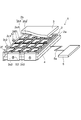
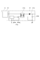
- FIG. 1 is a schematic perspective view for illustrating an X-ray detector 1.
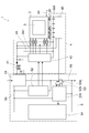
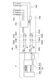
- FIG. 2 is a block diagram of the X-ray detector 1.
- FIG. 2 is a circuit diagram of an array substrate 2.
- FIG. It is a block diagram of the X-ray detector 100 which concerns on a comparative example.
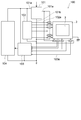
- 3 is a block diagram of a power supply circuit 41.
- FIG. 3 is a block diagram of a drive timing generation circuit 42.
- FIG. 3 is a block diagram of an image data signal transfer circuit 43.
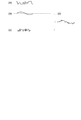
- FIG. (A)-(d) is a graph for demonstrating the noise in the X-ray detector 100 which concerns on a comparative example.
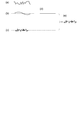
- (A) to (e) are graphs for illustrating noise when the power supply circuit 41 is provided.
- (A) to (f) are graphs for illustrating noise when the power supply circuit 41, the drive timing generation circuit 42, and the image data signal transfer circuit 43 are provided.
- the radiation detector according to the present embodiment can be applied to various types of radiation such as ⁇ rays in addition to X-rays.
- ⁇ rays in addition to X-rays.
- X-rays as a representative example of radiation will be described as an example. Therefore, by replacing “X-ray” in the following embodiments with “other radiation”, the present invention can be applied to other radiation.
- the X-ray detector 1 illustrated below is an X-ray plane sensor that detects an X-ray image that is a radiation image.
- X-ray flat sensors are roughly classified into direct conversion methods and indirect conversion methods.
- the direct conversion method is a method in which photoconductive charge (signal charge) generated inside the photoconductive film by incident X-rays is directly guided to a storage capacitor for charge storage by a high electric field.
- the indirect conversion method is a method in which X-rays are converted into fluorescence (visible light) by a scintillator, the fluorescence is converted into signal charges by a photoelectric conversion element such as a photodiode, and the signal charges are led to a storage capacitor.
- an indirect conversion type X-ray detector 1 is illustrated as an example, but the present invention can also be applied to a direct conversion type X-ray detector. That is, the X-ray detector only needs to have a detection unit that detects X-rays directly or in cooperation with the scintillator. Moreover, although the X-ray detector 1 can be used for general medical use etc., for example, there is no limitation in a use.
- FIG. 1 is a schematic perspective view for illustrating the X-ray detector 1.
- FIG. 2 is a block diagram of the X-ray detector 1.
- FIG. 3 is a circuit diagram of the array substrate 2. As shown in FIGS. 1 to 3, the X-ray detector 1 is provided with an array substrate 2, a scintillator 3, a signal processing unit 4, and a control processing unit 5.
- the array substrate 2 converts the fluorescence (visible light) converted from the X-rays by the scintillator 3 into an electric signal.
- the array substrate 2 includes a substrate 2a, a photoelectric conversion unit 2b, a control line (or gate line) 2c1, and a data line (or signal line) 2c2.
- the substrate 2a has a plate shape and is made of a translucent material such as non-alkali glass.
- a plurality of photoelectric conversion units 2b are provided on one surface of the substrate 2a.
- the photoelectric conversion unit 2b has a rectangular shape and is provided in a region defined by the control line 2c1 and the data line 2c2.
- the plurality of photoelectric conversion units 2b are arranged in a matrix.
- One photoelectric conversion unit 2b corresponds to one pixel.
- the photoelectric conversion unit 2 b serves as a detection unit that detects X-rays in cooperation with the scintillator 3.
- Each of the plurality of photoelectric conversion units 2b is provided with a photoelectric conversion element 2b1 and a thin film transistor (TFT) 2b2 which is a switching element. Further, as shown in FIG. 3, a storage capacitor 2b3 for storing the signal charge converted in the photoelectric conversion element 2b1 can be provided.
- the storage capacitor 2b3 has, for example, a rectangular flat plate shape and can be provided under each thin film transistor 2b2. However, depending on the capacitance of the photoelectric conversion element 2b1, the photoelectric conversion element 2b1 can also serve as the storage capacitor 2b3.
- the photoelectric conversion element 2b1 can be, for example, a photodiode.
- the thin film transistor 2b2 performs switching between accumulation and emission of electric charges generated when fluorescence enters the photoelectric conversion element 2b1.
- the thin film transistor 2b2 may include a semiconductor material such as amorphous silicon (a-Si) or polysilicon (P-Si).
- the thin film transistor 2b2 includes a gate electrode 2b2a, a source electrode 2b2b, and a drain electrode 2b2c. Gate electrode 2b2a of thin film transistor 2b2 is electrically connected to corresponding control line 2c1.
- the source electrode 2b2b of the thin film transistor 2b2 is electrically connected to the corresponding data line 2c2.
- the drain electrode 2b2c of the thin film transistor 2b2 is electrically connected to the corresponding photoelectric conversion element 2b1 and the storage capacitor 2b3.
- a plurality of control lines 2c1 are provided in parallel with each other at a predetermined interval.
- the control line 2c1 extends in the row direction (corresponding to an example of the first direction).
- One control line 2c1 is electrically connected to one of a plurality of wiring pads 2d1 provided near the periphery of the substrate 2a.
- One wiring pad 2d1 is electrically connected to one of a plurality of wirings provided on the flexible printed board 2e1.
- the other ends of the plurality of wirings provided on the flexible printed board 2e1 are electrically connected to the gate driver GD provided on the signal processing unit 4, respectively.
- a plurality of data lines 2c2 are provided in parallel with each other at a predetermined interval.
- the data line 2c2 extends in the column direction (corresponding to an example of the second direction) orthogonal to the row direction.
- One data line 2c2 is electrically connected to one of a plurality of wiring pads 2d2 provided near the periphery of the substrate 2a.
- One wiring pad 2d2 is electrically connected to one of a plurality of wirings provided on the flexible printed board 2e2.
- the other end of the wiring provided on the flexible printed circuit board 2 e 2 is electrically connected to the readout circuit RO provided on the signal processing unit 4.
- the control line 2c1 and the data line 2c2 can be formed using, for example, a low resistance metal such as aluminum or chromium.
- the protective layer 2f covers the photoelectric conversion unit 2b, the control line 2c1, and the data line 2c2.
- the protective layer 2f includes, for example, at least one of an oxide insulating material, a nitride insulating material, an oxynitride insulating material, and a resin material.
- the oxide insulating material include silicon oxide and aluminum oxide.
- the nitride insulating material include silicon nitride and aluminum nitride.
- the oxynitride insulating material is, for example, silicon oxynitride.
- the resin material is, for example, an acrylic resin.
- the scintillator 3 is provided on the plurality of photoelectric conversion elements 2b1 and converts incident X-rays into visible light, that is, fluorescence.
- the scintillator 3 is provided so as to cover an area (effective pixel area) where a plurality of photoelectric conversion units 2b are provided on the substrate 2a.
- the scintillator 3 can be formed using, for example, cesium iodide (CsI): thallium (Tl) or sodium iodide (NaI): thallium (Tl). In this case, if the scintillator 3 is formed using a vacuum vapor deposition method or the like, the scintillator 3 composed of an aggregate of a plurality of columnar crystals is formed.
- the thickness dimension of the scintillator 3 can be set to about 600 ⁇ m, for example.
- the thickness dimension of the pillar (pillar) of the columnar crystal can be, for example, about 8 ⁇ m to 12 ⁇ m
- the scintillator 3 can also be formed using, for example, gadolinium oxysulfide (Gd 2 O 2 S).
- the scintillator 3 can be formed as follows. First, particles made of gadolinium oxysulfide are mixed with a binder material. Next, the mixed material is applied so as to cover the effective pixel region. Next, the applied material is baked. Next, a groove is formed in the fired material using a blade dicing method or the like. At this time, a matrix-like groove portion can be formed so that the quadrangular columnar scintillator 3 is provided for each of the plurality of photoelectric conversion portions 2b.
- the groove portion can be filled with air (air) or an inert gas such as nitrogen gas for preventing oxidation. Moreover, you may make it a groove part be in a vacuum state.
- a reflection layer (not shown) can be provided so as to cover the surface side (X-ray incident surface side) of the scintillator 3 in order to improve the use efficiency of fluorescence and improve sensitivity characteristics.
- a moistureproof body (not shown) that covers the scintillator 3 and the reflective layer (not shown) can be provided.
- FIG. 4 is a block diagram of the X-ray detector 100 according to the comparative example.
- the X-ray detector 100 is provided with an array substrate 2, a scintillator 3, a system power supply circuit 101, a drive control circuit 102, a read control circuit 103, and an image processing circuit 104.
- the system power supply circuit 101 includes a DC / DC converter or the like, and converts a DC voltage supplied from the outside into a predetermined DC voltage.
- the system power supply circuit 101 applies the converted DC voltage to the drive control circuit 102, the read control circuit 103, the image processing circuit 104, the gate driver GD, and the read circuit RO.
- the drive control circuit 102 transmits a control signal to the corresponding gate driver GD in accordance with the scanning direction of the X-ray image.
- the gate driver GD Upon receiving the control signal from the drive control circuit 102, the gate driver GD applies a voltage to the corresponding control line 2c1.
- Each of the plurality of readout circuits RO has an integrating amplifier and an analog-digital converter.
- the read circuit RO amplifies the read image data signal and converts the amplified image data signal (analog signal) into a digital signal.
- the image data signal converted into the digital signal is transmitted to the read control circuit 103.
- the read control circuit 103 transmits the received image data signal to the image processing circuit 104.
- the image processing circuit 104 configures an X-ray image based on the image data signal from the readout control circuit 103.
- the DC / DC converter provided in the system power supply circuit 101 can generate a predetermined DC voltage by switching current, but generates switching noise (low frequency noise) at the time of switching.
- the generated switching noise enters the analog circuit such as the photoelectric conversion element 2b1 and the thin film transistor 2b2 provided in the photoelectric conversion unit 2b or the integration amplifier provided in the readout circuit RO through the power supply line 101a and the ground line 101b. Then, the quality of the obtained X-ray image may be significantly reduced.
- the number of photoelectric conversion portions 2b provided on the array substrate 2 is about several million. Therefore, a large number of gate drivers GD and readout circuits RO are required, and a complicated and large-scale digital circuit for controlling the large number of gate drivers GD and readout circuits RO is required. In digital circuits, high frequency digital noise is generated. If the generated digital noise enters an analog circuit such as an integral amplifier provided in the readout circuit RO via the signal lines 102a and 103a and the ground line 101b, the quality of the obtained X-ray image may be significantly deteriorated. .
- the number of signal lines 102a and 103a is reduced by performing two-dimensional scanning, there are several connections between the gate driver GD and the drive control circuit 102 and between the readout circuit RO and the readout control circuit 103. Ten to several hundred signal lines 102a and 103a are required. Therefore, noise due to signal skew is likely to occur. If the generated noise enters an analog circuit such as an integrating amplifier provided in the readout circuit RO via the ground line 101b, the quality of the obtained radiographic image may be significantly lowered.
- the signal processing unit 4 and the control processing unit 5 are separated in a DC manner. Further, the number of signal lines is further reduced.
- the signal processing unit 4 is provided on the opposite side of the array substrate 2 from the side on which the scintillator 3 is provided.
- the signal processing unit 4 is provided with a power supply circuit 41, a drive timing generation circuit 42, an image data signal transfer circuit 43, a plurality of gate drivers GD, and a plurality of readout circuits RO.
- the plurality of gate drivers GD are electrically connected to each of the plurality of control lines 2c1.
- the plurality of read circuits RO are electrically connected to each of the plurality of data lines 2c2.
- FIG. 5 is a block diagram of the power supply circuit 41.
- the power supply circuit 41 includes a DC-AC converter 41a, a transformer 41b, a rectifier 41c, and a capacitor 41d (corresponding to an example of a third capacitor).
- the DC-AC converter 41a converts the DC voltage supplied from the system power supply circuit 51 into an AC voltage.
- the DC-AC converter 41a includes an oscillation circuit 41a1 and a switching element 41a2.
- the oscillation circuit 41a1 turns on / off the switching element 41a2 at a predetermined frequency.
- the switching element 41a2 flows a pulsed current to the primary side of the transformer 41b by switching the current.
- the switching element 41a2 can be, for example, a bipolar transistor, an insulated gate bipolar transistor (IGBT), a MOSFET, a gate turn-off thyristor (GTO), or the like.
- IGBT insulated gate bipolar transistor
- GTO gate turn-off thyristor
- the primary side of the transformer 41b is electrically connected to the DC-AC converter 41a, and the secondary side is electrically connected to a plurality of readout circuits RO.
- the transformer 41b can be, for example, an insulating transformer or a shield transformer.
- the rectifying unit 41c is electrically connected between the secondary side of the transformer 41b and the plurality of readout circuits RO.
- the rectifying unit 41c rectifies the alternating current flowing on the secondary side of the transformer 41b.
- the rectifier 41c converts an alternating voltage into a direct voltage on the secondary side of the transformer 41b.
- the capacitor 41 d is electrically connected between the rectifying unit 41 c and the ground line 44.
- the power supply circuit 41 Since the power supply circuit 41 is provided with the transformer 41b, the signal processing unit 4 and the system power supply circuit 51 of the control processing unit 5 can be separated in a direct current manner. Therefore, the transformer 41b prevents the switching noise (low frequency noise) generated in the DC / DC converter provided in the system power supply circuit 51 from entering the photoelectric conversion element 2b1 and the thin film transistor 2b2 provided in the photoelectric conversion unit 2b. Can be suppressed. Further, switching noise generated in the DC-AC conversion unit 41a can be prevented from entering the photoelectric conversion element 2b1 and the thin film transistor 2b2 provided in the photoelectric conversion unit 2b. In addition, since the power supply circuit 41 is provided with the capacitor 41d, it is possible to suppress noise from entering the photoelectric conversion element 2b1 and the thin film transistor 2b2 provided in the photoelectric conversion unit 2b via the ground line 44. it can.
- FIG. 6 is a block diagram of the drive timing generation circuit 42.
- the drive timing generation circuit 42 is electrically connected between the drive control circuit 52 and the plurality of gate drivers GD.
- the drive timing generation circuit 42 receives serial data (corresponding to an example of first serial data) from a drive control circuit 52 described later, a plurality of start signals (signals for instructing the timing to start scanning), and a plurality of The clock signal (a signal for switching the control line 2c1) is restored, and the restored start signal and clock signal are transmitted to the corresponding gate driver GD. As shown in FIG.
- the drive timing generation circuit 42 includes buffers 42a1 and 42a2, inverters 42b1 and 42b2, capacitors 42c1, 42c2, 42c3, and 42c4 (corresponding to an example of a first capacitor), and operational amplifiers 42d1 and 42d2.
- a frequency divider 42e and a shift register 42f are provided.
- the start signal transmitted from the drive control circuit 52 is input to the buffer 42a1 and the inverter 42b1.
- the buffer 42a1 is not always necessary and can be omitted.
- the inverter 42b1 inverts the received start signal.
- the operational amplifier 42d1 calculates the difference between the start signal from the buffer 42a1 received via the capacitor 42c1 and the inverted signal from the inverter 42b1 received via the capacitor 42c2, and regenerates the start signal.
- the clock signal transmitted from the drive control circuit 52 is input to the buffer 42a2 and the inverter 42b2.
- the buffer 42a2 is not always necessary and can be omitted.
- the inverter 42b2 inverts the received clock signal.
- the operational amplifier 42d2 calculates the difference between the clock signal from the buffer 42a2 received via the capacitor 42c3 and the inverted signal from the inverter 42b2 received via the capacitor 42c4, and regenerates the clock signal.
- the regenerated clock signal is transmitted to the frequency dividing circuit 42e and the gate driver GD.
- the frequency dividing circuit 42e converts the received clock signal into a clock signal having a predetermined frequency and transmits it to the shift register 42f.
- the shift register 42f generates a control signal S1 for each of the plurality of gate drivers GD from the start signal from the operation amplifier 42d1 and the clock signal from the frequency dividing circuit 42e.
- the shift register 42f sequentially transmits the generated control signal S1 to each gate driver GD.
- the gate driver GD receives the control signal S1
- the gate driver GD applies a voltage to the corresponding control line 2c1.
- the thin film transistor 2b2 is turned on, and the signal charge (image data signal S2) from the photoelectric conversion element 2b1 can be received.
- the drive timing generation circuit 42 has capacitors 42c1, 42c2, 42c3, and 42c4 on the serial data receiving side. Therefore, the signal processing unit 4 and the control processing unit 5 can be separated in a direct current manner. As a result, low frequency noise can be prevented from entering the control processing unit 5 from the signal processing unit 4.
- the start signal and the clock signal are generated with reference to the ground potential. Therefore, the drive control circuit 102, the system power supply circuit 101, and the gate driver GD are connected to the common ground line 101b. As a result, switching noise generated in the system power supply circuit 101 may enter the gate driver GD via the ground line 101b.
- the start signal and the clock signal are generated with reference to the inverted signals generated by the inverters 42b1 and 42b2. Therefore, the ground line 55 to which the system power supply circuit 51 is connected and the ground line 44 to which the drive control circuit 42 and the gate driver GD are connected are separated. As a result, the switching noise generated in the system power supply circuit 51 can be prevented from entering the gate driver GD.
- the drive control circuit 52 and the drive timing generation circuit 42 need only be connected by two signal lines, generation of noise due to signal skew can be suppressed. Further, since the drive control circuit 52 does not require a complicated and large-scale digital circuit for generating signals for a large number of gate drivers GD, the digital circuit provided in the drive control circuit 52 can be simplified. . Therefore, it is possible to suppress the generation of high frequency digital noise in the drive control circuit 52.
- FIG. 7 is a block diagram of the image data signal transfer circuit 43.
- the image data signal transfer circuit 43 converts the image data signal S2 from each of the plurality of readout circuits RO into serial data (corresponding to an example of second serial data).
- the image data signal transfer circuit 43 includes a multiplication circuit 43a, a parallel-serial conversion circuit 43b, buffers 43c1, 43c2, inverters 43d1, 43d2, capacitors 43e1, 43e2, 43e3, 43e4 (second capacitors). And operational amplifiers 43f1 and 43f2 are provided.
- N image data signals S2 are read by N read circuits RO.
- the image data signal S2 is output in synchronization with the read clock signal.
- Each of the N readout circuits RO has an integrating amplifier and an analog-digital converter.
- the read circuit RO amplifies the read image data signal S2, and converts the amplified image data signal S2 (analog signal) into a digital signal.
- the image data signal S2 converted into a digital signal is transmitted to the parallel-serial conversion circuit 43b.
- the multiplier circuit 43a generates a transfer clock signal having a frequency N times the frequency of the read clock signal.
- the transfer clock signal is transmitted to the parallel-serial conversion circuit 43b, the buffer 43c2, and the inverter 43d2.
- the parallel-serial conversion circuit 43b sequentially outputs the image data signal S2 selectively from the N image data signals S2 in accordance with the transfer clock signal. That is, the parallel-serial conversion circuit 43b converts N pieces of parallel data into serial data.
- the converted serial data (image data signal S2) is input to the buffer 43c1 and the inverter 43d1.
- the buffer 43c1 is not always necessary and can be omitted.
- the inverter 43d1 inverts the received signal.
- the operational amplifier 43f1 calculates a difference between the signal from the buffer 43c1 received through the capacitor 43e1 and the inverted signal from the inverter 43d1 received through the capacitor 43e2, and transmits the difference to the control processing unit 5. Generate data.
- the transfer clock signal is input to the buffer 43c2 and the inverter 43d2.
- the buffer 43c2 is not always necessary and can be omitted.
- the inverter 43d2 inverts the received transfer clock signal.
- the operational amplifier 43f2 calculates the difference between the transfer clock signal from the buffer 43c2 received through the capacitor 43e3 and the inverted signal from the inverter 43d2 received through the capacitor 43e4, and transmits the difference to the control processing unit 5.
- the transfer clock signal is generated.
- the image data signal transfer circuit 43 includes capacitors 43e1, 43e2, 43e3, and 43e4 on the serial data transmission side. Therefore, the signal processing unit 4 and the control processing unit 5 can be separated in a direct current manner. As a result, low frequency noise can be prevented from entering the control processing unit 5 from the signal processing unit 4.
- a data signal to be transmitted to the read control circuit 103 is generated with reference to the ground potential. Therefore, the system power supply circuit 101, the read control circuit 103, and the read circuit RO are connected to the common ground line 101b. As a result, switching noise generated in the system power supply circuit 101 may enter the readout circuit RO through the ground line 101b.
- the read control circuit 53 since it is only necessary to connect the read control circuit 53 and the image data signal transfer circuit 43 by two signal lines, it is possible to suppress the occurrence of noise due to signal skew. Further, since the read control circuit 53 does not require a complicated and large-scale digital circuit for processing signals from a large number of read circuits RO, the digital circuit provided in the read control circuit 53 can be simplified. it can. Therefore, it is possible to suppress the generation of high-frequency digital noise in the read control circuit 53.
- the control processing unit 5 includes a system power supply circuit 51, a drive control circuit 52, a read control circuit 53, and an image processing circuit 54.
- the system power supply circuit 51 includes a DC / DC converter or the like, and converts a DC voltage supplied from the outside into a predetermined DC voltage.
- the system power supply circuit applies the converted DC voltage to the power supply circuit 41, the drive control circuit 52, the read control circuit 53, and the image processing circuit 54.
- the drive control circuit 52 generates a start signal and a clock signal for each of the plurality of gate drivers GD. Further, the drive control circuit 52 converts the generated plurality of start signals and the plurality of clock signals into serial data.
- the drive control circuit 52 transmits serial data to the drive timing generation circuit 42.
- the read control circuit 53 converts the serial data from the image data signal transfer circuit 43 into N pieces of parallel data, and transmits the converted parallel data to the image processing circuit 54.
- the read control circuit 53 restores the serial data from the image data signal transfer circuit 43 to a plurality of image data signals S2.
- the read control circuit 53 is provided with a frequency dividing circuit 53a, a serial-parallel conversion circuit 53b, and a transmission circuit 53c.
- the frequency dividing circuit 53a generates a clock signal having a frequency 1 / N times the frequency of the received transfer clock signal.
- the generated clock signal is transmitted to the serial-parallel conversion circuit 53b and the transmission circuit 53c.
- the serial-parallel conversion circuit 53b converts serial data (image data signal S2) into N pieces of parallel data in accordance with the clock signal.
- the transmission circuit 53 c transmits the converted parallel data to the image processing circuit 54.
- the image processing circuit 54 configures an X-ray image based on the image data signal S2 (parallel data) from the read control circuit 53.
- FIGS. 8A to 8D are graphs for illustrating noise in the X-ray detector 100 according to the comparative example.
- FIG. 8A shows switching noise (low frequency noise) in the power supply line 101a.
- FIG. 8B shows switching noise (low frequency noise) in the ground line 101b.
- FIG. 8C shows high-frequency noise such as digital noise generated on the control processing unit 5 side and noise generated due to signal skew.
- FIG. 8D shows the synthesized noise in the ground line 101b.
- noise entering through the power supply line 101a can be reduced by providing a filter in the power supply line 101a. That is, the noise illustrated in FIG. 8A can be reduced.
- FIGS. 9A to 9E are graphs for illustrating noise when the power supply circuit 41 is provided.
- FIG. 9A shows switching noise (low frequency noise) in the power supply line 56.
- FIG. 9B shows switching noise (low frequency noise) in the ground line 55.
- FIG. 9C shows high-frequency noise such as digital noise generated on the control processing unit 5 side and noise generated due to signal skew.
- FIG. 9D shows a state of low frequency noise in the ground line 44.
- FIG. 9E shows the synthesized noise in the ground line 44.
- the ground line 44 of the signal processing unit 4 and the ground line 55 of the control processing unit 5 can be separated. Therefore, as shown in FIG. 9D, it is possible to suppress the switching noise (low frequency noise) generated in the system power supply circuit 51 from entering the ground line 44.
- the high-frequency noise illustrated in FIG. 9C may enter the ground line 44.
- the noise illustrated in FIG. 9E may enter the readout circuit RO or the like via the ground line 44 or the like.
- FIGS. 10A to 10F are graphs for illustrating noise when the power supply circuit 41, the drive timing generation circuit 42, and the image data signal transfer circuit 43 are provided.
- FIG. 10A shows the switching noise (low frequency noise) in the power supply line 56.
- FIG. 10B shows switching noise (low frequency noise) in the ground line 55.
- FIG. 10C shows a state of low frequency noise in the ground line 44.
- FIG. 10D shows high-frequency noise such as digital noise generated on the control processing unit 5 side and noise generated due to signal skew.
- FIG. 10E shows a state of high frequency noise in the signal line on the signal processing unit 4 side.
- FIG. 10F shows the synthesized noise in the ground line 44.
- the ground line 44 of the signal processing unit 4 and the ground line 55 of the control processing unit 5 can be separated. Therefore, as shown in FIG. 10C, it is possible to suppress the switching noise (low frequency noise) generated in the system power supply circuit 51 from entering the ground line 44.
- the drive control circuit 52 and the drive timing generation circuit 42 can be connected by two signal lines.
- the image data signal transfer circuit 43 can also be connected by two signal lines. Therefore, as shown in FIG. 10E, it is possible to suppress the high frequency noise generated on the control processing unit 5 side from entering the signal line on the signal processing unit 4 side. As a result, as shown in FIG. 10F, noise that enters the readout circuit RO and the like via the ground line 44 can be greatly reduced.
Landscapes
- Engineering & Computer Science (AREA)
- Multimedia (AREA)
- Signal Processing (AREA)
- Physics & Mathematics (AREA)
- Health & Medical Sciences (AREA)
- Life Sciences & Earth Sciences (AREA)
- General Physics & Mathematics (AREA)
- High Energy & Nuclear Physics (AREA)
- Molecular Biology (AREA)
- Spectroscopy & Molecular Physics (AREA)
- Measurement Of Radiation (AREA)
- Transforming Light Signals Into Electric Signals (AREA)
- Solid State Image Pick-Up Elements (AREA)
Abstract
Description
この場合、電源ラインを介して侵入するノイズは、電源ラインにフィルタを設けることで低減させることができる。
ところが、グランドラインは共通となるため、グランドラインを介して侵入するノイズは除去することができない。
本実施の形態に係る放射線検出器は、X線のほかにもγ線などの各種放射線に適用させることができる。ここでは、一例として、放射線の中の代表的なものとしてX線に係る場合を例にとり説明をする。したがって、以下の実施形態の「X線」を「他の放射線」に置き換えることにより、他の放射線にも適用させることができる。
直接変換方式は、入射X線により光導電膜内部に発生した光導電電荷(信号電荷)を高電界により電荷蓄積用の蓄積キャパシタに直接導く方式である。
間接変換方式は、X線をシンチレータにより蛍光(可視光)に変換し、蛍光をフォトダイオードなどの光電変換素子により信号電荷に変換し、信号電荷を蓄積キャパシタに導く方式である。
以下においては、一例として、間接変換方式のX線検出器1を例示するが、本発明は直接変換方式のX線検出器にも適用することができる。
すなわち、X線検出器は、X線を直接的またはシンチレータと協働して検出する検出部を有するものであれば良い。
また、X線検出器1は、例えば、一般医療用途などに用いることができるが、用途に限定はない。
図2は、X線検出器1のブロック図である。
図3は、アレイ基板2の回路図である。
図1~図3に示すように、X線検出器1には、アレイ基板2、シンチレータ3、信号処理部4、および制御処理部5が設けられている。
アレイ基板2は、基板2a、光電変換部2b、制御ライン(又はゲートライン)2c1、およびデータライン(又はシグナルライン)2c2を有する。
基板2aは、板状を呈し、無アルカリガラスなどの透光性材料から形成されている。
光電変換部2bは、基板2aの一方の表面に複数設けられている。
光電変換部2bは、矩形状を呈し、制御ライン2c1とデータライン2c2とにより画された領域に設けられている。複数の光電変換部2bは、マトリクス状に並べられている。
なお、1つの光電変換部2bは、1つの画素(pixel)に対応する。
また、光電変換部2bは、X線をシンチレータ3と協働して検出する検出部となる。
また、図3に示すように、光電変換素子2b1において変換した信号電荷を蓄積する蓄積キャパシタ2b3を設けることができる。蓄積キャパシタ2b3は、例えば、矩形平板状を呈し、各薄膜トランジスタ2b2の下に設けることができる。ただし、光電変換素子2b1の容量によっては、光電変換素子2b1が蓄積キャパシタ2b3を兼ねることができる。
薄膜トランジスタ2b2は、蛍光が光電変換素子2b1に入射することで生じた電荷の蓄積および放出のスイッチングを行う。薄膜トランジスタ2b2は、アモルファスシリコン(a-Si)やポリシリコン(P-Si)などの半導体材料を含むものとすることができる。薄膜トランジスタ2b2は、ゲート電極2b2a、ソース電極2b2b及びドレイン電極2b2cを有している。薄膜トランジスタ2b2のゲート電極2b2aは、対応する制御ライン2c1と電気的に接続される。薄膜トランジスタ2b2のソース電極2b2bは、対応するデータライン2c2と電気的に接続される。薄膜トランジスタ2b2のドレイン電極2b2cは、対応する光電変換素子2b1と蓄積キャパシタ2b3とに電気的に接続される。
1つの制御ライン2c1は、基板2aの周縁近傍に設けられた複数の配線パッド2d1のうちの1つと電気的に接続されている。1つの配線パッド2d1には、フレキシブルプリント基板2e1に設けられた複数の配線のうちの1つが電気的に接続されている。フレキシブルプリント基板2e1に設けられた複数の配線の他端は、信号処理部4に設けられたゲートドライバGDとそれぞれ電気的に接続されている。
1つのデータライン2c2は、基板2aの周縁近傍に設けられた複数の配線パッド2d2のうちの1つと電気的に接続されている。1つの配線パッド2d2には、フレキシブルプリント基板2e2に設けられた複数の配線のうちの1つが電気的に接続されている。フレキシブルプリント基板2e2に設けられた配線の他端は、信号処理部4に設けられた読出回路ROと電気的に接続されている。
制御ライン2c1およびデータライン2c2は、例えば、アルミニウムやクロムなどの低抵抗金属を用いて形成することができる。
保護層2fは、例えば、酸化物絶縁材料、窒化物絶縁材料、酸窒化物絶縁材料、および樹脂材料の少なくとも1種を含む。
酸化物絶縁材料は、例えば、酸化シリコン、酸化アルミニウムなどである。
窒化物絶縁材料は、例えば、窒化シリコン、窒化アルミニウムなどである。
酸窒化物絶縁材料は、例えば、酸窒化シリコンなどである。
樹脂材料は、例えば、アクリル系樹脂などである。
シンチレータ3は、例えば、ヨウ化セシウム(CsI):タリウム(Tl)、あるいはヨウ化ナトリウム(NaI):タリウム(Tl)などを用いて形成することができる。この場合、真空蒸着法などを用いて、シンチレータ3を形成すれば、複数の柱状結晶の集合体からなるシンチレータ3が形成される。
シンチレータ3の厚み寸法は、例えば、600μm程度とすることができる。柱状結晶の柱(ピラー)の太さ寸法は、例えば、最表面で8μm~12μm程度とすることができる。
また、空気中に含まれる水蒸気により、シンチレータ3の特性と図示しない反射層の特性が劣化するのを抑制するために、シンチレータ3と図示しない反射層を覆う図示しない防湿体を設けることができる。
図4は、比較例に係るX線検出器100のブロック図である。
図4に示すように、X線検出器100には、アレイ基板2、シンチレータ3、システム電源回路101、駆動制御回路102、読出し制御回路103、および画像処理回路104が設けられている。
ゲートドライバGDは、駆動制御回路102からの制御信号を受信すると、対応する制御ライン2c1に電圧を印加する。
画像処理回路104は、読出し制御回路103からの画像データ信号に基づいてX線画像を構成する。
デジタル回路においては、高周波のデジタルノイズが発生する。発生したデジタルノイズが、信号ライン102a、103aやグランドライン101bを介して、読出回路ROに設けられた積分増幅器などのアナログ回路に侵入すると、得られるX線画像の品質が著しく低下するおそれがある。
図1に示すように、信号処理部4は、アレイ基板2の、シンチレータ3が設けられる側とは反対側に設けられている。
また、図2に示すように、信号処理部4には、電源回路41、駆動タイミング生成回路42、画像データ信号転送回路43、複数のゲートドライバGD、および複数の読出回路ROが設けられている。
複数のゲートドライバGDは、複数の制御ライン2c1のそれぞれに電気的に接続されている。
複数の読出回路ROは、複数のデータライン2c2のそれぞれに電気的に接続されている。
図5に示すように、電源回路41には、DC-AC変換部41a、トランス41b、整流部41c、およびコンデンサ41d(第3のコンデンサの一例に相当する)が設けられている。
DC-AC変換部41aは、システム電源回路51から供給された直流電圧を交流電圧に変換する。
DC-AC変換部41aは、発振回路41a1とスイッチング素子41a2を有する。
発振回路41a1は、所定の周波数でスイッチング素子41a2をON/OFFさせる。
スイッチング素子41a2は、電流をスイッチングすることで、トランス41bの一次側にパルス状の電流を流す。スイッチング素子41a2は、例えば、バイポーラトランジスタ、絶縁ゲートバイポーラトランジスタ(IGBT)、MOSFET、ゲートターンオフサイリスタ(GTO)などとすることができる。
トランス41bは、例えば、絶縁トランス、シールドトランスなどとすることができる。
整流部41cは、トランス41bの二次側と複数の読出回路ROとの間に電気的に接続されている。整流部41cは、トランス41bの二次側に流れる交流電流を整流する。整流部41cは、トランス41bの二次側において、交流電圧を直流電圧に変換する。
コンデンサ41dは、整流部41cとグランドライン44との間に電気的に接続されている。
また、電源回路41には、コンデンサ41dが設けられているので、グランドライン44を介して、光電変換部2bに設けられた光電変換素子2b1や薄膜トランジスタ2b2にノイズが侵入するのを抑制することができる。
駆動タイミング生成回路42は、駆動制御回路52と複数のゲートドライバGDとの間に電気的に接続されている。
駆動タイミング生成回路42は、後述する駆動制御回路52からのシリアルデータ(第1のシリアルデータの一例に相当する)を複数のスタート信号(走査を開始するタイミングを指示するための信号)と複数のクロック信号(制御ライン2c1を切り替えるための信号)とに復元し、復元されたスタート信号とクロック信号を対応するゲートドライバGDに送信する。
図6に示すように、駆動タイミング生成回路42には、バッファ42a1、42a2、インバータ42b1、42b2、コンデンサ42c1、42c2、42c3、42c4(第1のコンデンサの一例に相当する)、作動アンプ42d1、42d2、分周回路42e、および、シフトレジスタ42fが設けられている。
ゲートドライバGDは、制御信号S1を受信すると、対応する制御ライン2c1に電圧を印加する。制御ライン2c1に電圧が印加されると、薄膜トランジスタ2b2がON状態となり、光電変換素子2b1からの信号電荷(画像データ信号S2)が受信できるようになる。
画像データ信号転送回路43は、複数の読出回路ROのそれぞれからの画像データ信号S2をシリアルデータ(第2のシリアルデータの一例に相当する)に変換する。
図7に示すように、画像データ信号転送回路43には、逓倍回路43a、パラレル-シリアル変換回路43b、バッファ43c1、43c2、インバータ43d1、43d2、コンデンサ43e1、43e2、43e3、43e4(第2のコンデンサの一例に相当する)、作動アンプ43f1、43f2が設けられている。
また、N個の読出回路ROのそれぞれは、積分増幅器と、アナログ-デジタル変換器を有する。読出回路ROは、読み出された画像データ信号S2を増幅し、増幅された画像データ信号S2(アナログ信号)をデジタル信号に変換する。デジタル信号に変換された画像データ信号S2は、パラレル-シリアル変換回路43bに送信される。
システム電源回路51は、DC/DCコンバータなどを有し、外部から供給された直流電圧を所定の直流電圧に変換する。システム電源回路は、電源回路41、駆動制御回路52、読出し制御回路53、および画像処理回路54に変換された直流電圧を印加する。
駆動制御回路52は、複数のゲートドライバGDのそれぞれに対してスタート信号とクロック信号とを生成する。また、駆動制御回路52は、生成した複数のスタート信号と複数のクロック信号とをシリアルデータに変換する。駆動制御回路52は、シリアルデータを駆動タイミング生成回路42に送信する。
読出し制御回路53は、画像データ信号転送回路43からのシリアルデータを複数の画像データ信号S2に復元する。
図7に示すように、読出し制御回路53には、分周回路53a、シリアル-パラレル変換回路53b、および送信回路53cが設けられている。
分周回路53aは、受信した転送クロック信号の周波数の1/N倍の周波数を有するクロック信号を生成する。生成されたクロック信号は、シリアル-パラレル変換回路53bおよび送信回路53cに送信される。
送信回路53cは、変換されたパラレルデータを画像処理回路54に送信する。
図8(a)~(d)は、比較例に係るX線検出器100におけるノイズを例示するためのグラフ図である。
なお、図8(a)は、電源ライン101aにおけるスイッチングノイズ(低周波ノイズ)を表している。図8(b)は、グランドライン101bにおけるスイッチングノイズ(低周波ノイズ)を表している。図8(c)は、制御処理部5側で発生したデジタルノイズや信号のスキューにより発生したノイズなどの高周波ノイズを表している。図8(d)は、グランドライン101bにおける合成されたノイズを表している。
なお、図9(a)は電源ライン56におけるスイッチングノイズ(低周波ノイズ)を表している。図9(b)は、グランドライン55におけるスイッチングノイズ(低周波ノイズ)を表している。図9(c)は、制御処理部5側で発生したデジタルノイズや信号のスキューにより発生したノイズなどの高周波ノイズを表している。図9(d)は、グランドライン44における低周波ノイズの状態を表している。図9(e)は、グランドライン44における合成されたノイズを表している。
なお、図10(a)は電源ライン56におけるスイッチングノイズ(低周波ノイズ)を表している。図10(b)は、グランドライン55におけるスイッチングノイズ(低周波ノイズ)を表している。図10(c)は、グランドライン44における低周波ノイズの状態を表している。図10(d)は、制御処理部5側で発生したデジタルノイズや信号のスキューにより発生したノイズなどの高周波ノイズを表している。図10(e)は、信号処理部4側の信号ラインにおける高周波ノイズの状態を表している。図10(f)は、グランドライン44における合成されたノイズを表している。
Claims (5)
- 第1の方向に延びる複数の制御ラインと、前記第1の方向に交差する第2の方向に延びる複数のデータラインと、前記複数の制御ラインと前記複数のデータラインとにより画された複数の領域のそれぞれに設けられ、対応する前記制御ラインと対応する前記データラインとに電気的に接続され、放射線を直接的またはシンチレータと協働して検出する検出部と、を有するアレイ基板と、
前記複数の制御ラインのそれぞれに電気的に接続されたゲートドライバと、
複数の前記ゲートドライバのそれぞれに対してスタート信号とクロック信号とを生成し、生成した複数の前記スタート信号と複数の前記クロック信号とを第1のシリアルデータに変換する駆動制御回路と、
前記駆動制御回路と前記複数のゲートドライバとの間に電気的に接続され、前記第1のシリアルデータを複数の前記スタート信号と複数の前記クロック信号とに復元し、前記復元されたスタート信号とクロック信号を対応する前記ゲートドライバに送信する駆動タイミング生成回路と、
前記複数のデータラインのそれぞれに電気的に接続された読出回路と、
複数の前記読出回路のそれぞれからの画像データ信号を第2のシリアルデータに変換する画像データ信号転送回路と、
前記第2のシリアルデータを複数の前記画像データ信号に復元する読出し制御回路と、
を備えた放射線検出器。 - 外部から供給された直流電圧を所定の直流電圧に変換するシステム電源回路と、
前記システム電源回路から供給された直流電圧を交流電圧に変換するDC-AC変換部と、
一次側が前記DC-AC変換部と電気的に接続され、二次側が前記複数の読出回路と電気的に接続されたトランスと、
前記トランスの二次側と前記複数の読出回路との間に電気的に接続された整流部と、
をさらに備えた請求項1記載の放射線検出器。 - 前記駆動タイミング生成回路は、前記第1のシリアルデータを受信する側に第1のコンデンサを有している請求項1または2に記載の放射線検出器。
- 前記画像データ信号転送回路は、前記第2のシリアルデータを送信する側に第2のコンデンサを有している請求項1~3のいずれか1つに記載の放射線検出器。
- 前記整流部とグランドとの間に電気的に接続された第3のコンデンサをさらに備えた請求項2~4のいずれか1つに記載の放射線検出器。
Priority Applications (4)
| Application Number | Priority Date | Filing Date | Title |
|---|---|---|---|
| KR1020187029607A KR102057181B1 (ko) | 2016-04-15 | 2017-02-16 | 방사선 검출기 |
| CN201780022729.0A CN108886597A (zh) | 2016-04-15 | 2017-02-16 | 放射线检测器 |
| EP17782109.7A EP3445041B1 (en) | 2016-04-15 | 2017-02-16 | Radiation detector |
| US16/158,419 US20190049600A1 (en) | 2016-04-15 | 2018-10-12 | Radiation detector |
Applications Claiming Priority (2)
| Application Number | Priority Date | Filing Date | Title |
|---|---|---|---|
| JP2016081957A JP2017192090A (ja) | 2016-04-15 | 2016-04-15 | 放射線検出器 |
| JP2016-081957 | 2016-04-15 |
Related Child Applications (1)
| Application Number | Title | Priority Date | Filing Date |
|---|---|---|---|
| US16/158,419 Continuation US20190049600A1 (en) | 2016-04-15 | 2018-10-12 | Radiation detector |
Publications (1)
| Publication Number | Publication Date |
|---|---|
| WO2017179290A1 true WO2017179290A1 (ja) | 2017-10-19 |
Family
ID=60041758
Family Applications (1)
| Application Number | Title | Priority Date | Filing Date |
|---|---|---|---|
| PCT/JP2017/005653 Ceased WO2017179290A1 (ja) | 2016-04-15 | 2017-02-16 | 放射線検出器 |
Country Status (7)
| Country | Link |
|---|---|
| US (1) | US20190049600A1 (ja) |
| EP (1) | EP3445041B1 (ja) |
| JP (1) | JP2017192090A (ja) |
| KR (1) | KR102057181B1 (ja) |
| CN (1) | CN108886597A (ja) |
| TW (1) | TWI649863B (ja) |
| WO (1) | WO2017179290A1 (ja) |
Families Citing this family (4)
| Publication number | Priority date | Publication date | Assignee | Title |
|---|---|---|---|---|
| JP6869914B2 (ja) * | 2018-03-06 | 2021-05-12 | 富士フイルム株式会社 | 放射線画像検出装置 |
| TWI734489B (zh) * | 2020-05-22 | 2021-07-21 | 睿生光電股份有限公司 | X射線裝置及其製造方法 |
| JP2022012182A (ja) * | 2020-07-01 | 2022-01-17 | キヤノン電子管デバイス株式会社 | 放射線検出器 |
| KR102474979B1 (ko) * | 2021-01-12 | 2022-12-06 | 주식회사 파프리카랩 | 피부 부착형 방사선 측정 장치를 이용한 방사선 피폭 모니터링 시스템 |
Citations (3)
| Publication number | Priority date | Publication date | Assignee | Title |
|---|---|---|---|---|
| JP2005087254A (ja) * | 2003-09-12 | 2005-04-07 | Canon Inc | 画像読出装置及びx線撮影装置 |
| WO2011161988A1 (ja) * | 2010-06-23 | 2011-12-29 | コニカミノルタエムジー株式会社 | 放射線画像撮影装置 |
| JP2013070168A (ja) * | 2011-09-21 | 2013-04-18 | Toshiba Corp | 平面型x線センサ |
Family Cites Families (10)
| Publication number | Priority date | Publication date | Assignee | Title |
|---|---|---|---|---|
| JP4457613B2 (ja) * | 2003-09-04 | 2010-04-28 | ソニー株式会社 | 固体撮像装置 |
| EP1515163B1 (en) * | 2003-09-12 | 2009-07-29 | Canon Kabushiki Kaisha | Image reading apparatus and x-ray imaging apparatus |
| US20060186315A1 (en) * | 2005-02-22 | 2006-08-24 | Kany-Bok Lee | Active pixel image sensors |
| JP2006238444A (ja) * | 2005-02-22 | 2006-09-07 | Samsung Electronics Co Ltd | アクティブピクセルイメージセンサ |
| JP5322060B2 (ja) * | 2009-12-21 | 2013-10-23 | 東芝電子管デバイス株式会社 | 放射線画像読取装置 |
| JP5665484B2 (ja) * | 2010-10-29 | 2015-02-04 | キヤノン株式会社 | 撮像装置、放射線撮影システム、イメージセンサの制御方法 |
| JP2012118312A (ja) * | 2010-12-01 | 2012-06-21 | Fujifilm Corp | 放射線画像検出装置およびその駆動制御方法 |
| JP6114635B2 (ja) * | 2013-06-06 | 2017-04-12 | 東芝電子管デバイス株式会社 | 放射線検出器およびその製造方法 |
| JP6226579B2 (ja) * | 2013-06-13 | 2017-11-08 | 東芝電子管デバイス株式会社 | 放射線検出器及びその製造方法 |
| KR20150061704A (ko) * | 2013-11-27 | 2015-06-05 | 삼성전자주식회사 | 엑스선 검출기, 이를 포함하는 엑스선 영상 장치 및 그 제어 방법 |
-
2016
- 2016-04-15 JP JP2016081957A patent/JP2017192090A/ja active Pending
-
2017
- 2017-02-16 CN CN201780022729.0A patent/CN108886597A/zh not_active Withdrawn
- 2017-02-16 WO PCT/JP2017/005653 patent/WO2017179290A1/ja not_active Ceased
- 2017-02-16 KR KR1020187029607A patent/KR102057181B1/ko active Active
- 2017-02-16 EP EP17782109.7A patent/EP3445041B1/en not_active Not-in-force
- 2017-02-24 TW TW106106556A patent/TWI649863B/zh active
-
2018
- 2018-10-12 US US16/158,419 patent/US20190049600A1/en not_active Abandoned
Patent Citations (3)
| Publication number | Priority date | Publication date | Assignee | Title |
|---|---|---|---|---|
| JP2005087254A (ja) * | 2003-09-12 | 2005-04-07 | Canon Inc | 画像読出装置及びx線撮影装置 |
| WO2011161988A1 (ja) * | 2010-06-23 | 2011-12-29 | コニカミノルタエムジー株式会社 | 放射線画像撮影装置 |
| JP2013070168A (ja) * | 2011-09-21 | 2013-04-18 | Toshiba Corp | 平面型x線センサ |
Non-Patent Citations (1)
| Title |
|---|
| See also references of EP3445041A4 * |
Also Published As
| Publication number | Publication date |
|---|---|
| EP3445041B1 (en) | 2021-03-24 |
| US20190049600A1 (en) | 2019-02-14 |
| JP2017192090A (ja) | 2017-10-19 |
| KR20180122424A (ko) | 2018-11-12 |
| EP3445041A1 (en) | 2019-02-20 |
| EP3445041A4 (en) | 2019-10-23 |
| KR102057181B1 (ko) | 2019-12-18 |
| TW201739041A (zh) | 2017-11-01 |
| TWI649863B (zh) | 2019-02-01 |
| CN108886597A (zh) | 2018-11-23 |
Similar Documents
| Publication | Publication Date | Title |
|---|---|---|
| CN101682687B (zh) | 放射线检测设备和放射线成像系统 | |
| US7573041B2 (en) | Imaging apparatus, radiation imaging apparatus, and radiation imaging system | |
| CN103247645B (zh) | 摄像装置、其制造方法以及摄像显示系统 | |
| US20160161616A1 (en) | Radiation detector | |
| CN103491284B (zh) | 摄像部、摄像单元及摄像显示系统 | |
| CN103247644B (zh) | 成像设备及其制造方法和成像显示系统 | |
| WO2017179290A1 (ja) | 放射線検出器 | |
| US10156643B2 (en) | Radiation detector | |
| US20150369930A1 (en) | Radiographic imaging detector using voltage conversion on glass | |
| CN102446931A (zh) | 检测装置和辐射检测系统 | |
| JP2016156719A (ja) | 放射線検出器 | |
| US20180348382A1 (en) | Radiation detector | |
| US20180164448A1 (en) | Radiaton detector | |
| JP6404661B2 (ja) | 放射線検出器用アレイ基板、および放射線検出器 | |
| JP6164924B2 (ja) | 検出装置、及び、検出システム | |
| WO2017134896A1 (ja) | X線撮像素子の製造方法 | |
| TWI620948B (zh) | Photoelectric conversion array substrate and radiation detector | |
| JP6953186B2 (ja) | 放射線検出器 | |
| WO2022244276A1 (ja) | 放射線検出器 | |
| JP2019113443A (ja) | 放射線検出器 | |
| JP2019012774A (ja) | 放射線検出器 | |
| JP2019070538A (ja) | 放射線検出器、放射線検出システム、および補正に関するデータの回収方法 |
Legal Events
| Date | Code | Title | Description |
|---|---|---|---|
| ENP | Entry into the national phase |
Ref document number: 20187029607 Country of ref document: KR Kind code of ref document: A |
|
| NENP | Non-entry into the national phase |
Ref country code: DE |
|
| WWE | Wipo information: entry into national phase |
Ref document number: 2017782109 Country of ref document: EP |
|
| ENP | Entry into the national phase |
Ref document number: 2017782109 Country of ref document: EP Effective date: 20181115 |
|
| 121 | Ep: the epo has been informed by wipo that ep was designated in this application |
Ref document number: 17782109 Country of ref document: EP Kind code of ref document: A1 |