WO2017183563A1 - デジタルフィルタ装置、デジタルフィルタ処理方法およびプログラム記録媒体 - Google Patents
デジタルフィルタ装置、デジタルフィルタ処理方法およびプログラム記録媒体 Download PDFInfo
- Publication number
- WO2017183563A1 WO2017183563A1 PCT/JP2017/015211 JP2017015211W WO2017183563A1 WO 2017183563 A1 WO2017183563 A1 WO 2017183563A1 JP 2017015211 W JP2017015211 W JP 2017015211W WO 2017183563 A1 WO2017183563 A1 WO 2017183563A1
- Authority
- WO
- WIPO (PCT)
- Prior art keywords
- data
- bit width
- circuit
- input
- filter
- Prior art date
- Legal status (The legal status is an assumption and is not a legal conclusion. Google has not performed a legal analysis and makes no representation as to the accuracy of the status listed.)
- Ceased
Links
Images


Classifications
-
- G—PHYSICS
- G06—COMPUTING OR CALCULATING; COUNTING
- G06F—ELECTRIC DIGITAL DATA PROCESSING
- G06F17/00—Digital computing or data processing equipment or methods, specially adapted for specific functions
- G06F17/10—Complex mathematical operations
- G06F17/14—Fourier, Walsh or analogous domain transformations, e.g. Laplace, Hilbert, Karhunen-Loeve, transforms
- G06F17/141—Discrete Fourier transforms
- G06F17/142—Fast Fourier transforms, e.g. using a Cooley-Tukey type algorithm
-
- H—ELECTRICITY
- H03—ELECTRONIC CIRCUITRY
- H03H—IMPEDANCE NETWORKS, e.g. RESONANT CIRCUITS; RESONATORS
- H03H17/00—Networks using digital techniques
- H03H17/02—Frequency selective networks
- H03H17/0211—Frequency selective networks using specific transformation algorithms, e.g. WALSH functions, Fermat transforms, Mersenne transforms, polynomial transforms, Hilbert transforms
- H03H17/0213—Frequency domain filters using Fourier transforms
-
- H—ELECTRICITY
- H03—ELECTRONIC CIRCUITRY
- H03H—IMPEDANCE NETWORKS, e.g. RESONANT CIRCUITS; RESONATORS
- H03H17/00—Networks using digital techniques
- H03H17/02—Frequency selective networks
- H03H17/0223—Computation saving measures; Accelerating measures
- H03H17/0233—Measures concerning the signal representation
- H03H17/0235—Measures concerning the signal representation reducing the wordlength of signals
Definitions
- the present invention relates to a digital filter device that performs digital signal processing, a digital filter processing method, and a program recording medium.
- FFT Fast Fourier transform
- FFT Fast Fourier Transform
- FFT Fast Fourier Transform
- signal data in the time domain is converted into data in the frequency domain by FFT, and then filter processing for equalization is performed.
- the filtered data is reconverted into signal data in the time domain by inverse fast Fourier transform (hereinafter IFFT: Inverse FFT), and the waveform distortion of the signal in the original time domain is compensated.
- IFFT Inverse FFT
- Non-Patent Document 1 discloses butterfly computation by Cooley-Tukey, which is an efficient FFT / IFFT processing method. By the way, the butterfly computation by Cooley-Tukey has a problem that the FFT / IFFT circuit becomes complicated when the number of points is large.
- Non-Patent Document 2 discloses a Prime Factor method for decomposing an operation with a large number of points into two small FFT / IFFT.
- Patent Document 2 page 5, FIG. 2 and FIG. 3
- Patent Document 3 page 5, FIG. 1
- storage means such as RAM (Random Access Memory) or a register is used for data rearrangement (for example, Patent Document 3 (page 5, FIG. 1), Patent Document 4 (pages 9-10, (See Fig. 3)).
- Floating point arithmetic has the advantage of being able to perform arithmetic operations with high accuracy even when the range of signal data values to be handled is wide.
- Floating point arithmetic has the advantage of being able to perform arithmetic operations with high accuracy even when the range of signal data values to be handled is wide.
- fixed point arithmetic has an advantage that the circuit size and power consumption are small because the circuit is simple, but there is a problem that arithmetic accuracy is low.
- the calculation by the block floating point has the advantages of both floating point and fixed point. In the calculation by the block floating point, a plurality of signal data is collected as one block, and is normalized in the whole block so that each block has a common index.
- Patent Document 4 by performing adaptive equalization processing on a time domain signal in the frequency domain instead of the time domain, an increase in circuit scale and an increase in operating clock frequency can be suppressed.
- it is unnecessary in order to implement
- An object of the present invention is to provide a digital filter device that can reduce the circuit scale and power consumption while maintaining the filter performance in order to solve the above-described problems.
- a digital filter device includes a first conversion circuit that performs a first conversion process on data in a predetermined frequency range, and data that has been subjected to the first conversion process by the first conversion circuit in advance.
- a filter processing circuit that executes the filtering process by setting the calculation bit width of the set data of the first frequency component to a bit width different from the data of the other frequency components, and the data that has been subjected to the filtering process by the filter processing circuit
- a second conversion circuit for executing a second conversion process.
- a first conversion process is performed on data in a predetermined frequency range, and a first frequency component set in advance among the data subjected to the first conversion process.
- the data processing bit width is set to a bit width different from that of other frequency component data, the filtering process is executed, and the second conversion process is executed on the filtered data.
- a program recording medium includes a process for executing a first conversion process on data in a predetermined frequency range, and a first frequency component set in advance among the data subjected to the first conversion process.
- FFT Fast Fourier Transform
- IFFT inverse fast Fourier transform
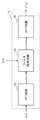
- FIG. 1 is a block diagram showing the configuration of the digital filter device 11 of the present embodiment.
- the digital filter device 11 includes an FFT circuit 21, a filter processing circuit 31, and an IFFT circuit 41.
- the FFT circuit 21 inputs a complex signal x (n) in the time domain.
- n is an integer of 0 ⁇ n ⁇ N ⁇ 1 indicating a signal sample number in the time domain
- N is a natural number indicating the number of FFT conversion samples (FFT block size).
- the complex signal x (n) is expressed as the following Expression 1 using the real part r (n), the imaginary part s (n), and the imaginary unit j.
- x (n) r (n) + js (n) (1)
- the FFT circuit 21 converts the input complex signal x (n) into a complex signal X (k) in the frequency domain by FFT.
- k is an integer of 0 ⁇ k ⁇ N ⁇ 1 indicating a frequency number in the frequency domain.
- the complex signal X (k) is expressed by the following equation 2 using the real part A (k), the imaginary part B (k), and the imaginary unit j.
- X (k) A (k) + jB (k) (2)
- the FFT circuit 21 outputs the complex signal X (k) to the filter processing circuit 31.
- the filter processing circuit 31 performs complex filter processing by complex multiplication on the complex signal X (k) input from the FFT circuit 21 using the filter coefficient C (k), and outputs the complex signal X ′ (k). calculate.
- the complex signal X ′ (k) is calculated by the following equation 3.
- X ′ (k) X (k) ⁇ C (k) (3)
- the filter processing circuit 31 outputs the calculated complex signal X ′ (k) to the IFFT circuit 41.
- the IFFT circuit 41 generates a time-domain complex signal x ′′ (n) by IFFT with respect to the input complex signal X ′ (k).
- the IFFT circuit 41 outputs the generated complex signal x ′′ (n).
- FIG. 2 is used to show a data flow 100 for executing a 64-point FFT decomposed into two-stage radix-8 butterfly computation processing by the Prime Factor method.
- FIG. 2 includes a data rearrangement process 101, a butterfly operation process 102, a butterfly operation process 103, and a twist multiplication process 104.
- a total of 16 radix-8 butterfly computation processes are executed.
- the data flow 100 in FIG. 2 has the same basic configuration when performing IFFT processing.
- the entire FFT processing may be realized by repeatedly using a circuit that realizes processing of a part of the data flow 100 according to the required processing performance.
- processing corresponding to each of the partial data flows 105a to 105h performed for 8 data is sequentially performed.
- the partial data flow 105c, the partial data flow 105d, the partial data flow 105e, the partial data flow 105f, and the partial data flow 105g are omitted.
- the process corresponding to the partial data flow 105a is performed for the first time, and the process corresponding to the partial data flow 105b is performed for the second time.
- the third time corresponds to the partial data flow 105c
- the fourth time corresponds to the partial data flow 105d
- the fifth time corresponds to the partial data flow 105e
- the sixth time corresponds to the partial data flow 105f
- the seventh time corresponds to the partial data flow 105g.
- the processing to be performed is performed sequentially.
- processing corresponding to the partial data flow 105h is performed.
- a 64-point FFT process can be realized by the series of processes described above.
- FIG. 3 is a block diagram illustrating a configuration example of the FFT circuit 21.
- the FFT circuit 21 includes a first data rearrangement processing circuit 211, a first butterfly operation processing circuit 212, a second data rearrangement processing circuit 213, a twist multiplication processing circuit 214, and a second butterfly operation processing circuit 215. Is provided.
- the FFT circuit 21 uses each component in FIG. 3 to perform first data rearrangement processing, first butterfly operation processing, second data rearrangement processing, and twist multiplication as in the data flow 100 in FIG. Pipeline processing including processing and second butterfly calculation processing is executed.
- the first data rearrangement processing circuit 211 is a buffer circuit for rearranging data.
- the first data rearrangement processing circuit 211 rearranges the data sequence based on the algorithm data dependency in the FFT process.
- the first data rearrangement processing circuit 211 outputs the rearranged data to the first butterfly calculation processing circuit 212.
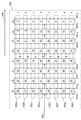
- the first data rearrangement processing circuit 211 rearranges the input data x (n) from the sequential order (FIG. 4) to the bit reverse order (FIG. 5). That is, the first data rearrangement processing circuit 211 changes the input data x (n) from the sequential order (FIG. 4) as the input order to the bit reverse order (FIG. 5) as the output order to the first butterfly operation processing circuit 212. ).
- Each row ps (i) in FIG. 4 and each row qs (i) in FIG. 5 indicate data input to the i-th in the next stage.
- Eight numbers included in each data set are identification information for uniquely specifying one of the points of the FFT, specifically, the value of the subscript n of x (n).
- the bit reverse order shown in FIG. 5 corresponds to the input data set to the radix-8 butterfly computation process 102 in the first stage in the data flow 100 shown in FIG. Specifically, in the first cycle, eight pieces of data of x (0), x (8),..., X (56) constituting the data set Q1 are input. Then, in the second cycle, eight data of x (1), x (9),..., X (57) constituting the data set Q2 are input. Thereafter, in the same manner from the 3rd cycle to the 8th cycle, 8 data constituting the data sets Q3 to Q8 are input.
- the first butterfly operation processing circuit 212 is a butterfly circuit that executes the first butterfly operation processing 102 (first butterfly operation processing) in the radix-8 butterfly operation processing performed twice in the data flow 100 of FIG. is there.
- the first butterfly calculation processing circuit 212 executes butterfly calculation processing on the data rearranged by the first data rearrangement processing circuit 211.
- the second data rearrangement processing circuit 213 is a buffer circuit for data rearrangement.
- the second data rearrangement processing circuit 213 rearranges the data sequence based on the algorithm data dependency in the FFT processing after the butterfly computation by the first butterfly computation processing circuit 212.
- the second data rearrangement processing circuit 213 rearranges the data y (n) output in the sequential order by the first butterfly operation processing circuit 212 into the bit reverse order for input to the second butterfly operation processing circuit 215.
- the second data rearrangement processing circuit 213 outputs the rearranged data to the twist multiplication processing circuit 214.
- the twist multiplication processing circuit 214 is a circuit that processes complex rotation on the complex plane in the FFT calculation after the first butterfly calculation process.
- the twist multiplication processing circuit 214 executes a twist multiplication process corresponding to the twist multiplication process 104 in the data flow 100 of FIG.
- the twist multiplication processing circuit 214 outputs the data y ′ (n) subjected to the twist multiplication processing to the second butterfly computation processing circuit 215. Note that the twist multiplication processing circuit 214 does not rearrange data in the twist multiplication processing.
- the second butterfly operation processing circuit 215 is a butterfly circuit that executes the second radix-8 butterfly operation processing 103 (second butterfly operation processing) in the data flow 100 of FIG.
- “Sequential order” means the order of eight data sets P1, P2, P3, P4, P5, P6, P7, and P8, as shown in FIG.
- Ps (i) is expressed by the following formula 4.
- ps (i) 8 (s ⁇ 1) + i (4)
- Each data set is arranged in the order of P1, P2, P3, P4, P5, P6, P7, and P8 corresponding to the progress of the processing cycle.
- the sequential order is created by creating s data sets in which i ⁇ s pieces of data are arranged i in order from the top data in the order of the data, and arranging these data sets in the cycle order.
- the “bit reverse order” means the order of eight data sets Q1, Q2, Q3, Q4, Q5, Q6, Q7, Q8 as shown in FIG.
- Each of the data sets Qs includes eight pieces of data from qs (0) to qs (7).
- qs (i) is represented by the following formula 5.
- qs (i) (s-1) + 8i (5)
- Each data set is arranged in the order of Q1, Q2, Q3, Q4, Q5, Q6, Q7, and Q8 corresponding to the progress of the processing cycle.
- bit reverse order is a sequence in which i ⁇ s pieces of data input in a sequential order are arranged in s order from the top data in order of cycles, and i pieces of data in the same cycle are arranged in order of data as one set. It is.
- each data set in the bit reverse order is uniquely determined if each sequential order is set.
- Qs (i) Pi (s) (6)
- Qs (i) and Pi (s) have a relationship in which the order of the cycle progress and the order of the data position are exchanged for the data constituting each data set. Therefore, when data input in the bit reverse order is rearranged according to the bit reverse order, the sequential order is obtained.
- each sequential data set may be created by arranging data in order according to the number of FFT points, the number of cycles, and the number of data to be processed in parallel. Then, as described above, each data set in the bit reverse order may be created by exchanging the order with respect to the progress of the cycle and the order with respect to the data position for the data input in the sequential order.
- the FFT circuit 21 processes a 64-point FFT that has been decomposed into two-stage radix-8 butterfly processing by a pipeline circuit method.
- the FFT circuit 21 performs 64-point FFT processing in parallel with 8 data.
- a total of 64 pieces of input data x (n) are inputted to the FFT circuit 21 in the sequential order shown in FIG.
- the numbers 0 to 63 shown in the table of FIG. 4 correspond to n in the parentheses of the input data x (n).
- a total of 64 pieces of output data X (k) are output from the FFT circuit 21 in the order shown in FIG.
- the numbers 0 to 63 shown in the table of FIG. 4 correspond to k in the parentheses of the output data X (k).
- the first data rearrangement processing circuit 211 and the second data rearrangement processing circuit 213 temporarily store the input data, control the selection and output of the stored data, and perform sequential order (FIG. 4) and bit reverse order ( The data rearrangement process according to each of FIGS.
- the first data rearrangement processing circuit 211 and the second data rearrangement processing circuit 213 can be realized by, for example, the data rearrangement processing circuit 200 shown in FIG.
- the data rearrangement processing circuit 200 inputs the data sets D1 to D8 (input information 203) composed of eight data in the first-in first-out buffer (hereinafter referred to as FIFO buffer: First In First Out Buffer). Then, the data rearrangement processing circuit 200 writes and stores data in the data storage positions 201a to 201h. Specifically, the data rearrangement processing circuit 200 stores the data sets D1 to D8 in the data storage positions 201a to 201h, respectively.
- FIFO buffer First In First Out Buffer
- the data rearrangement processing circuit 200 outputs the stored data in the first-out order in the FIFO buffer. Specifically, the data rearrangement processing circuit 200 sets eight data read from each of the data reading positions 202a to 202h as one data set, and uses the eight data sets D1 ′ to D8 ′ (output information 204). Output. That is, the data sets D1 'to D8' are obtained by rearranging the data included in the data sets D1 to D8 arranged in the cycle order in the order of the data positions.
- the first data rearrangement processing circuit 211 and the second data rearrangement processing circuit 213 perform rearrangement according to each of the sequential order (FIG. 4) and the bit reverse order (FIG. 5). Replacement processing is required. This is because, since the FFT circuit 21 performs 64-point FFT processing in parallel with 8 data, 8 cycles are required for the FFT processing, and data must be rearranged across the cycles.
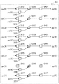
- FIG. 7 is a block diagram illustrating a configuration example of the filter processing circuit 31 of the present embodiment.
- the filter processing circuit 31 includes bit width reduction circuits 310 to 317, bit width reduction circuits 320 to 327, complex multipliers 330 to 337, and bit width expansion circuits 340 to 347.
- the filter processing circuit 31 performs filter operation processing in parallel with 8 data, like the FFT circuit 21.
- the frequency processing data X (k) output from the FFT circuit 21 in the bit reverse order is input to the filter processing circuit 31.
- 64 data is input as input data X (k) in a bit reverse order shown in FIG.
- k in parentheses of X (k) means a number from 0 to 63 in FIG. That is, in the first cycle, 8 data of X (0), X (1),..., X (7) constituting the data set Q1 are input to the filter processing circuit 31. In the second cycle, 8 data of X (8), X (9),..., X (15) constituting the data set Q2 are input to the filter processing circuit 31. Similarly, data constituting the data sets Q3 to Q8 are input to the filter processing circuit 31 from the third cycle to the eighth cycle. Similarly, the filter processing circuit 31 receives 64 data filter coefficients C (k) in the order of bit reverse in a period of 8 cycles of 8 data.
- bit width reduction circuits 310 to 317 of the filter processing circuit 31 reduce the bit width of the data X (k) inputted by 8 data.
- Bit width reduction circuits 310 to 317 output data with the reduced bit width to complex multipliers 330 to 337.
- the bit width reduction circuit 310 generates data X ′ (k) obtained by reducing the bit width of X (k) input from the input px (0).
- the bit width reduction circuit 311 generates data X ′ (k) obtained by reducing the bit width of X (k) input from the input px (1).
- each of the bit width reduction circuits 312 to 317 generates X ′ (k) by reducing the bit width of X (k) input from the inputs px (2) to px (7).
- the bit width can be reduced by a truncation process or a rounding process. Note that the amount of bit width reduction performed by the bit width reduction circuits 310 to 317 may be the same in each circuit, or may be different in each circuit.
- bit width reduction circuits 320 to 327 of the filter processing circuit 31 reduce the bit width of the filter coefficient C (k) inputted by 8 data.
- Bit width reduction circuits 320 to 327 output data with reduced bit widths to complex multipliers 330 to 337.
- the bit width reduction circuit 320 generates C ′ (k) in which the bit width of C (k) input from the input pc (0) is reduced.
- the bit width reduction circuit 321 generates C ′ (k) by reducing the bit width of C (k) input from the input pc (1).
- each of the bit width reduction circuits 321 to 327 generates C ′ (k) obtained by reducing the bit width of C (k) input from the inputs pc (2) to pc (7).
- the bit width can be reduced by a truncation process or a rounding process. Note that the amount of bit width reduction performed by the bit width reduction circuits 320 to 327 may be the same in each circuit, or may be different in each circuit.
- the complex multipliers 330 to 337 of the filter processing circuit 31 use the data X ′ (k) with the reduced bit width and the filter coefficient C ′ (k) to perform complex multiplication that performs complex multiplication in 8-data parallel. Perform filtering.
- the complex multipliers 333 to 337 input X ′ (j) input from the input px (k) and reduce the bit width, and C ′ (j) input from the input pc (k) and reduced the bit width.
- k and j in parentheses of px (k), pc (k), X ′ (j), C ′ (j), and Y (j) are also called frequency numbers.
- the complex multipliers 333 to 337 input X ′ (j + 1) input from the input px (k) and reduce the bit width, and C ′ (j + 1) input from the input pc (k) and reduced the bit width.
- C ′ (j + 1) input from the input pc (k) and reduced the bit width.
- the complex multiplier 330 includes eight data of X ′ (0), X ′ (1),..., X ′ (7), and C ′ (0), C ′ (1),. 8 data of C ′ (7) is input, 8 data of Y (0), Y (1),..., Y (7) is calculated and output.
- the complex multiplier 331 includes 8 data of X ′ (8), X ′ (9),..., X ′ (15), and C ′ (8), C ′ (9),. , C ′ (15) and 8 data of Y (8), Y (9),..., Y (15) are calculated and output.
- the complex multiplier 332 includes 8 data of X ′ (16), X ′ (17),..., X ′ (23), C ′ (16), C ′ (17),. , C ′ (23) and 8 data, Y (16), Y (17),..., Y (23) are calculated and output.
- the complex multiplier 333 inputs 8 data of X ′ (24) to X ′ (31) and 8 data of C ′ (24) to C ′ (31), and Y (24) to Y
- the 8 data of (31) is calculated and output.
- the complex multiplier 334 inputs 8 data of X ′ (32) to X ′ (39) and 8 data of C ′ (32) to C ′ (39), and Y (32) to Y
- the 8 data of (39) is calculated and output.
- the complex multiplier 335 inputs 8 data of X ′ (40) to X ′ (47) and 8 data of C ′ (40) to C ′ (47), and Y (40) to Y ′.
- the eight data of (47) are calculated and output.
- the complex multiplier 336 inputs 8 data of X ′ (48) to X ′ (55) and 8 data of C ′ (48) to C ′ (55), and Y (48) to Y ′.
- the eight data of (55) are calculated and output.
- the complex multiplier 337 inputs 8 data of X ′ (56) to X ′ (63) and 8 data of C ′ (56) to C ′ (63), and Y (56) to Y The eight data of (63) are calculated and output.
- each of the complex multipliers 330 to 337 receives data adjacent to frequency numbers as input, and calculates and outputs data adjacent to frequency numbers.
- the bit width reduction amounts performed by the bit width reduction circuits 310 to 317 and the bit width reduction circuits 320 to 327 may be different. That is, the calculation bit widths in each of the complex multipliers 330 to 337 may be different. Therefore, the bit widths of the outputs of the complex multipliers 330 to 337 may be different.
- bit width expansion circuits 340 to 347 perform bit width expansion on Y (k) that is calculated and output by the complex multipliers 330 to 337, and output data py (0) to py Output to (7).
- the bit width can be expanded by adding a necessary number of values 0 to the least significant bits of the data, for example.
- the bit width extension circuit 340 has the same bit width for the outputs py (0) to py (7) according to the bit width of Y (k) input from the complex multiplier 330. The bit width is extended, and the data with the bit width extended is output to the output py (0).
- the bit width extension circuit 341 has a bit width so that the outputs py (0) to py (7) have the same bit width according to the bit width of Y (k) input from the complex multiplier 331. The data with the bit width extended is output to the output py (1).
- each of the bit width extension circuits 342 to 347 has the same bit in the outputs py (0) to py (7) according to the bit width of Y (k) input from the complex multipliers 332 to 337. Extend the bit width to be the width. Then, each of the bit width extension circuits 342 to 347 outputs data with the bit width extended to outputs py (2) to py (7).
- the filter process in a certain frequency range may not be important as compared with the filter process in another frequency range.
- the filter performance is improved. The influence of is small. That is, even if the calculation bit width of the complex multiplier that performs filtering in an insignificant frequency range is reduced, the filter performance may not be reduced, or desired filter characteristics may be obtained even if the filter performance is reduced. In such a case, the calculation bit width of a complex multiplier that performs filtering processing in an insignificant frequency range can be made smaller than the calculation bit width of a complex multiplier that performs filtering processing in another frequency range.
- the filter processing circuit 31 of the present embodiment sets the operation bit widths of a plurality of complex multipliers that perform filter processing according to the importance of the frequency range to be filtered. In other words, the filter processing circuit 31 reduces the calculation bit width in the complex multiplier that performs the filter processing of the data in the frequency range with low importance.
- the frequency range with low importance is a range including frequency components that can obtain desired filter characteristics even if the bit width of data in the frequency range is reduced.
- the filtering process in the high frequency region may be less important than the filtering process in other frequency regions.
- the calculation bit width of the complex multiplier that performs the filtering process in the high frequency region can be made smaller than the calculation bit width of the other complex multipliers.
- filter processing in a low frequency region may be less important than other frequency region filter processing.
- the calculation bit width of the complex multiplier that performs the filtering process in the low frequency region can be made smaller than the calculation bit width of the other complex multipliers.
- the filtering process in a specific frequency domain may be less important than the filtering process in other frequency domains.
- the calculation bit width of the complex multiplier that performs the filtering process in a specific frequency region can be made smaller than the calculation bit width of the other complex multipliers.
- the filter processing circuit 31 sets the operation bit width of the first frequency component data set in advance in the data converted by the FFT circuit 21 to a smaller bit width than the data of the other frequency components. Perform filtering.
- the first frequency component set in advance is a component that can obtain a desired filter characteristic even if the bit width of the data of the frequency component is changed.
- FIG. 8 is a block diagram illustrating a configuration example of the IFFT circuit 41 of the present embodiment.
- the IFFT circuit 41 is a data flow similar to the FFT data flow 100 shown in FIG. 2, and processes the 64-point IFFT decomposed into two-stage radix-8 butterfly computation processing by a pipeline circuit method.
- the IFFT circuit 41 performs 64-point IFFT processing in parallel with 8 data. Similarly to the outputs of the FFT circuit 21 and the filter processing circuit 31, the IFFT circuit 41 inputs the data X (k) in the bit reverse order shown in FIG. Then, IFFT circuit 41 outputs data y (n) in the sequential order shown in FIG.
- the IFFT circuit 41 includes a first butterfly arithmetic processing circuit 411, a first data rearrangement processing circuit 412, a twist multiplication processing circuit 413, a second butterfly arithmetic processing circuit 414, and a second data rearrangement processing circuit 415.
- the IFFT circuit 41 performs the first butterfly operation process, the first data rearrangement process, the twist multiplication process, the second butterfly operation process, and the second data rearrangement process by using each component of FIG. Execute pipeline processing including.
- the first butterfly operation processing circuit 411 is a butterfly circuit that executes the first butterfly operation processing 102 (first butterfly operation processing) in the radix-8 butterfly operation processing performed twice in the data flow 100 of FIG. is there.
- the first data rearrangement processing circuit 412 is a buffer circuit for rearranging data.
- the first data rearrangement processing circuit 412 can be realized by the data rearrangement processing circuit 200 shown in FIG.
- the first data rearrangement processing circuit 412 rearranges the data sequence based on the data dependency on the algorithm in the IFFT process. Specifically, the first data rearrangement processing circuit 412 inputs the data y (n) output in the sequential order by the first butterfly computation processing circuit 411 to the bit multiplication order 413 in order to input the data y (n). Rearrange to Fig. 5).
- the twist multiplication processing circuit 413 is a circuit that processes a complex rotation on the complex plane in the IFFT calculation after the first butterfly calculation process.
- the twist multiplication processing circuit 413 executes a twist multiplication process corresponding to the twist multiplication process 104 in the data flow 100 of FIG.
- the twist multiplication processing circuit 413 outputs the data y ′ (n) subjected to the twist multiplication processing to the second butterfly computation processing circuit 414. Note that the twist multiplication processing circuit 413 does not rearrange data in the twist multiplication processing.
- the second butterfly operation processing circuit 414 is a butterfly circuit that executes the second radix-8 butterfly operation processing 103 (second butterfly operation processing) in the data flow 100 of FIG.
- the second data rearrangement processing circuit 415 is a buffer circuit for rearranging data.
- the second data rearrangement processing circuit 415 can be realized by the data rearrangement processing circuit 200 shown in FIG.
- the second data rearrangement processing circuit 415 rearranges the data sequence based on the data dependency on the algorithm in the IFFT process. Specifically, the second data rearrangement processing circuit 415 rearranges the data X (k) output by the second butterfly operation processing circuit 414 in the bit reverse order in the sequential order (FIG. 4). Then, the IFFT circuit 41 outputs the final result of the IFFT processing in sequential order.
- the calculation bit width of the complex multiplier that performs filtering processing in an insignificant frequency range is made smaller than the calculation bit width of the complex multiplier that performs filtering processing in other frequency ranges. .
- sufficient filter performance can be obtained with respect to other processing in a desired frequency range, and the complex multiplier that performs filtering in an insignificant frequency range can be simplified. That is, according to the present embodiment, the circuit scale and power consumption can be reduced without reducing the filter performance.
- the digital filter device of this embodiment differs from the first embodiment in the configuration of the filter processing circuit. Note that the configurations of the FFT circuit and IFFT circuit of the digital filter device of the present embodiment are the same as those of the first embodiment, and thus detailed description thereof is omitted.
- FIG. 9 is a block diagram showing the configuration of the digital filter device 12 of the present embodiment.
- the digital filter device 12 includes an FFT circuit 22, a filter processing circuit 32, and an IFFT circuit 42. Note that the FFT circuit 22 and the IFFT circuit 42 of the present embodiment have the same configuration as the FFT circuit 21 and the IFFT circuit 41 of the first embodiment, and thus detailed description thereof is omitted.
- FIG. 10 is a block diagram showing a configuration example of the filter processing circuit 32 of the present embodiment.
- the filter processing circuit 32 includes bit width reduction circuits 313 and 314, bit width reduction circuits 323 and 324, complex multipliers 333 and 334, and bit width expansion circuits 343 and 344. That is, the filter processing circuit 32 is different from the filter processing circuit 31 in FIG. 7 except for the bit width reduction circuits 313 and 314, the bit width reduction circuits 323 and 324, the complex multipliers 333 and 334, and the bit width expansion circuits 343 and 344. Is omitted.
- the filter processing circuit 32 has a configuration in which only the arithmetic bit widths of the complex multipliers 333 and 334 that perform filter processing in a high frequency range are reduced.
- the filter processing circuit 32 does not reduce the operation bit width of the complex multipliers 330 to 332 and 335 to 337 that perform filter processing in other frequency ranges. In the present embodiment, the importance of the high frequency range is low.
- the frequency domain data X (k) output by the FFT circuit 21 in the bit reverse order is input.
- the filter processing circuit 32 inputs 64 data of input data X (k) in a bit reverse order (FIG. 6) in a period of 8 cycles of 8 data.
- each of the complex multipliers 330 to 337 receives data having adjacent frequency numbers as input, and calculates and outputs data having adjacent frequency numbers.
- High frequency range data is input to the complex multiplier 333 and the complex multiplier 334, and a filter operation is performed on the high frequency range data.
- the filter processing in the high frequency range may be less important than the filter processing in other frequency ranges.
- the filter processing circuit of the present embodiment makes the operation bit width of the complex multiplier that performs the filter processing in the high frequency range smaller than the operation bit width of the complex multiplier that performs the filter processing in the other frequency range. Can do.
- the circuit scale and power consumption can be reduced without reducing the filter performance.
- FIG. 11 is a block diagram showing the configuration of the digital filter device 10 of the present embodiment.
- the digital filter device 10 includes a first conversion circuit 20, a filter processing circuit 30, and a second conversion circuit 40.
- the first conversion circuit 20 receives a plurality of data and performs a first conversion process on the input data x (n).
- the first conversion circuit 20 executes an FFT conversion process or an IFFT conversion process as the first conversion process.
- the filter processing circuit 30 sets the calculation bit width of the data of the first frequency component set in advance among the data subjected to the first conversion processing by the first conversion circuit 20 to a bit width different from the data of the other frequency components. And execute the filtering process.
- the first frequency component set in advance is a frequency component with which desired filter characteristics can be obtained even if the bit width of the data of the frequency component is changed.
- the filter processing circuit 30 includes an arithmetic circuit in which frequency component data that can obtain desired filter characteristics even when the arithmetic bit width is changed is set as the first frequency component data.
- the filter processing circuit 30 performs the filter process by reducing the calculation bit width of the data of the first frequency component.
- the filter processing circuit 30 includes an arithmetic circuit in which the arithmetic bit width of the data of the first frequency component is set to a bit width smaller than the arithmetic bit width of the data in the other frequency range.
- the filter processing circuit 30 reduces the operation bit width of data having low importance among a plurality of data.
- the filter processing circuit 30 performs arithmetic processing between a plurality of data including data with a reduced bit width and filter coefficients input separately.
- the filter processing circuit 30 outputs the data after expanding the bit width of the data having a small bit width included in the data subjected to the arithmetic processing to the same number of bits as other data.
- the second conversion circuit 40 performs a second conversion process on the plurality of data X (n) output from the filter processing circuit 30.
- the second conversion circuit 40 executes the FFT conversion process or the IFFT conversion process as the second conversion process.
- the second transform circuit 40 executes the inverse Fourier transform process when the first transform circuit 20 executes the fast Fourier transform process, and executes the inverse fast Fourier transform process when the first transform circuit 20 executes the inverse fast Fourier transform process. Perform Fourier transform processing.
- the data processed by the filter processing circuit 30 and the data arrangement can be expressed as follows.
- the first conversion circuit 20 receives the first data in either the first or second order, and generates the second data by executing the first conversion process on the input first data. Are output in the second order.
- the filter processing circuit 30 inputs the second data in the second order, and outputs the third data generated by executing the filter process on the input second data in the second order.
- the second conversion circuit 40 inputs the third data in the second order, and performs the second conversion process on the input third data to generate the fourth data generated by the first and second data. Output in either of the following order.
- the first order is a sequential order
- the second order is a bit reverse order.
- the first data is input data to the first conversion circuit 20
- the second data is output data from the first conversion circuit 20
- the third data is from the filter processing circuit 30.
- This is output data
- the fourth data is an output from the second conversion circuit 40. That is, the first data is input data to the digital filter device 10, and the fourth data is output data from the digital filter device 10.
- FIG. 12 is a block diagram showing the configuration of the filter processing circuit 30 of the present embodiment.
- the filter processing circuit 30 includes a first bit width reduction circuit 301, a second bit width reduction circuit 302, an arithmetic circuit 303, and a bit width extension circuit 304.
- the first bit width reduction circuit 301 receives the data converted by the first conversion circuit 20 and changes the bit width of the first frequency component data in the input data. For example, the first bit width reduction circuit 301 reduces the bit width of the data of the first frequency component. For example, the first bit width reduction circuit 301 reduces the bit width of data using either a truncation process or a rounding process.
- the first bit width reduction circuit 301 corresponds to a configuration including the bit width reduction circuits 310 to 317 of the first and second embodiments.
- the first bit width reduction circuit 301 receives the second data, and reduces the bit width of any of the input second data.
- the second bit width reduction circuit 302 reduces the bit width with respect to a filter coefficient for executing filter processing on the data whose bit width has been reduced by the first bit width reduction circuit 301.
- the second bit width reduction circuit 302 reduces the bit width of the filter coefficient using either a truncation process or a rounding process.
- the second bit width reduction circuit 302 corresponds to a configuration including the bit width reduction circuits 320 to 327 of the first and second embodiments.
- the second bit width reduction circuit 302 receives the filter coefficient data for executing the filter processing, and reduces the bit width of the filter coefficient corresponding to the data whose bit width has been reduced by the first bit width reduction circuit 301. To do.
- the arithmetic circuit 303 performs arithmetic processing on each of a plurality of data including data whose bit width has been reduced by the first bit width reduction circuit 301.
- the arithmetic circuit 303 includes a plurality of arithmetic units, and for data with a reduced bit width, performs an operation using a filter coefficient with a reduced bit width.
- the arithmetic circuit 303 corresponds to a configuration including the complex multipliers 330 to 337 of the first and second embodiments.
- the arithmetic circuit 303 has a filter coefficient including the second data including the data whose bit width is reduced by the first bit width reduction circuit 301 and the filter coefficient whose bit width is reduced by the second bit width reduction circuit 302. Perform operations using data.
- the bit width extension circuit 304 aligns the bit widths of a plurality of data output from the arithmetic circuit 303. In other words, the bit width extension circuit 304 aligns the data whose bit width has been reduced by the first bit width reduction circuit 301 with the same bit width as other data by inserting 0 at the end.
- the bit width extension circuit 304 corresponds to a configuration including the bit width extension circuits 340 to 347 of the first and second embodiments.
- bit width expansion circuit 304 expands the bit width of the data filtered by the arithmetic circuit 303 among the data whose bit width has been reduced by the first bit width reduction circuit 301.
- the circuit scale and power consumption can be reduced without reducing the filter performance.
- the hardware 90 for realizing the digital filter device according to the present embodiment will be described with reference to FIG.
- the hardware 90 is an example for realizing the digital filter device of the present embodiment, and does not limit the scope of the present invention.
- the hardware 90 includes a processor 91, a main storage device 92, an auxiliary storage device 93, an input / output interface 95, and a network adapter 96.
- the processor 91, main storage device 92, auxiliary storage device 93, input / output interface 95, and network adapter 96 are connected to each other via a bus 99.
- the processor 91, the main storage device 92, the auxiliary storage device 93, and the input / output interface 95 are connected to a network such as an intranet or the Internet via a network adapter 96.
- the hardware 90 is connected to another system or device via a network. Note that each of the components of the hardware 90 may be single or plural.
- the processor 91 is a central processing unit that expands a program stored in the auxiliary storage device 93 or the like in the main storage device 92 and executes the expanded program. In the present embodiment, a configuration using a software program installed in the hardware 90 may be used. The processor 91 executes various arithmetic processes and control processes.
- the main storage device 92 has an area where the program is expanded.
- the main storage device 92 may be a volatile memory such as a DRAM (Dynamic Random Access Memory). Further, a nonvolatile memory such as MRAM (Magnetoresistive Random Access Memory) may be configured and added as the main storage device 92.
- DRAM Dynamic Random Access Memory
- MRAM Magnetic Random Access Memory
- the auxiliary storage device 93 is means for storing various data.
- the auxiliary storage device 93 is configured as a local disk such as a hard disk or a flash memory.
- the main storage device 92 may be configured to store data, and the auxiliary storage device 93 may be omitted.
- the input / output interface 95 is an interface (I / F) that connects the hardware 90 and peripheral devices based on a connection standard.
- the hardware 90 may be connected to input devices such as a keyboard, a mouse, and a touch panel as necessary. These input devices are used for inputting information and settings.
- input devices such as a keyboard, a mouse, and a touch panel as necessary.
- the display screen of the display device may be a touch panel display that also serves as an interface of the input device.
- Data exchange between the processor 91 and the input device may be mediated by the input / output interface 95.
- the network adapter 96 is an interface for connecting to a network such as the Internet or an intranet based on standards or specifications.
- the input / output interface 95 and the network adapter 96 may be shared as an interface for connecting to an external device.
- the hardware 90 may be provided with a reader / writer as necessary.
- the reader / writer is connected to the bus 99 and reads a data program from the recording medium and writes the processing result of the hardware 90 to the recording medium between the processor 91 and a recording medium (program recording medium) (not shown).
- the recording medium can be realized by a semiconductor recording medium such as an SD (Secure Digital) card or a USB (Universal Serial Bus) memory.
- the recording medium may be realized by a magnetic recording medium such as a flexible disk, an optical recording medium such as a CD (Compact Disc) or a DVD (Digital Versatile Disc), or other recording media.
- the above is an example of the hardware configuration for enabling the digital filter device according to the embodiment of the present invention.
- the hardware configuration in FIG. 13 is an example of a hardware configuration that enables the digital filter device according to the present embodiment, and does not limit the scope of the present invention.
- a processing program that causes a computer to execute processing by the digital filter device according to the present embodiment is also included in the scope of the present invention.
- a program recording medium that records the processing program according to the embodiment of the present invention is also included in the scope of the present invention.
Landscapes
- Physics & Mathematics (AREA)
- Mathematical Physics (AREA)
- Engineering & Computer Science (AREA)
- General Physics & Mathematics (AREA)
- Theoretical Computer Science (AREA)
- Mathematical Analysis (AREA)
- Mathematical Optimization (AREA)
- Pure & Applied Mathematics (AREA)
- Computational Mathematics (AREA)
- Data Mining & Analysis (AREA)
- Algebra (AREA)
- Computing Systems (AREA)
- Computer Hardware Design (AREA)
- Software Systems (AREA)
- General Engineering & Computer Science (AREA)
- Databases & Information Systems (AREA)
- Discrete Mathematics (AREA)
- Complex Calculations (AREA)
Abstract
Description
まず、本発明の第1の実施形態に係るデジタルフィルタ装置について図面を参照しながら説明する。以下において、高速フーリエ変換のことをFFT(Fast Fourier Transform)、逆高速フーリエ変換のことをIFFT(Inverse FFT)と記載する。
x(n)=r(n)+js(n)・・・(1)
FFT回路21は、入力された複素数信号x(n)を、FFTによって周波数領域の複素数信号X(k)に変換する。kは、周波数領域上の周波数番号を示す0≦k≦N-1の整数である。複素数信号X(k)は、実部A(k)、虚部B(k)および虚数単位jを用いて、以下の式2のように表される。
X(k)=A(k)+jB(k)・・・(2)
FFT回路21は、複素数信号X(k)をフィルタ処理回路31に出力する。
X’(k)=X(k)×C(k)・・・(3)
フィルタ処理回路31は、算出した複素数信号X’(k)をIFFT回路41に出力する。
ここで、図2を用いて、2段階の基数8のバタフライ演算処理に分解された64ポイントFFTをPrime Factor法によって実行するデータフロー100を示す。
図3は、FFT回路21の構成例を示すブロック図である。図3のように、FFT回路21は、第1データ並べ替え処理回路211、第1バタフライ演算処理回路212、第2データ並べ替え処理回路213、ひねり乗算処理回路214および第2バタフライ演算処理回路215を備える。FFT回路21は、図3の各構成要素を用いて、図2のデータフロー100のように、第1のデータ並べ替え処理、第1のバタフライ演算処理、第2のデータ並べ替え処理、ひねり乗算処理および第2のバタフライ演算処理を含むパイプライン処理を実行する。
ps(i)=8(s-1)+i・・・(4)
そして、各データ組は、処理のサイクルの進行に対応して、P1、P2、P3、P4、P5、P6、P7、P8の順に並べられている。つまり、逐次順序とは、i×s個のデータを先頭のデータからi個ずつデータ順に並べたデータ組をs個作成し、それらのデータ組をサイクル順に並べたものである。
qs(i)=(s-1)+8i・・・(5)
そして、各データ組は、処理のサイクルの進行に対応して、Q1、Q2、Q3、Q4、Q5、Q6、Q7、Q8の順に並べられている。つまり、ビットリバース順序とは、逐次順序で入力されたi×s個のデータを、先頭のデータからs個ずつサイクル順に並べ、同じサイクルのi個のデータを1つの組としてデータ順に並べたものである。
Qs(i)=Pi(s)・・・(6)
このように、Qs(i)とPi(s)とは、各データ組を構成するデータについて、サイクルの進行に対する順序と、データ位置に対する順序とが入れ替えられた関係にある。したがって、ビットリバース順序で入力されたデータを、ビットリバース順序に従って並べ替えると逐次順序になる。
図7は、本実施形態のフィルタ処理回路31の構成例を示すブロック図である。フィルタ処理回路31は、ビット幅縮小回路310~317、ビット幅縮小回路320~327、複素乗算器330~337およびビット幅拡張回路340~347を備える。
図8は、本実施形態のIFFT回路41の構成例を示すブロック図である。IFFT回路41は、図2に示すFFTのデータフロー100と同様のデータフローで、2段階の基数8のバタフライ演算処理に分解された64ポイントIFFTをパイプライン回路方式によって処理する。
以上のように、本実施形態においては、重要ではない周波数範囲のフィルタ処理を行う複素乗算器の演算ビット幅を、他の周波数範囲のフィルタ処理を行う複素乗算器の演算ビット幅よりも小さくする。その結果、本実施形態においては、所望の周波数範囲の他処理に関しては十分なフィルタ性能が得られ、重要ではない周波数範囲のフィルタ処理を行う複素乗算器に関しては簡略化できる。すなわち、本実施形態によれば、フィルタ性能を低下させずに、回路規模や消費電力を低減することができる。
次に、本発明の第2の実施形態に係るデジタルフィルタ装置について図面を参照しながら説明する。本実施形態のデジタルフィルタ装置は、フィルタ処理回路の構成が第1の実施形態とは異なる。なお、本実施形態のデジタルフィルタ装置のFFT回路およびIFFT回路の構成は、第1の実施形態と同様であるため、詳細な説明は省略する。
次に、本発明の第3の実施形態に係るデジタルフィルタ装置について図面を参照しながら説明する。本実施形態は、第1および第2の実施形態を上位概念化した構成である。
ここで、フィルタ処理回路30の構成について図面を参照しながら説明する。図12は、本実施形態のフィルタ処理回路30の構成を示すブロック図である。図12のように、フィルタ処理回路30は、第1ビット幅縮小回路301、第2ビット幅縮小回路302、演算回路303およびビット幅拡張回路304を含む。
ここで、図13を用いて、本実施形態に係るデジタルフィルタ装置を実現するハードウェア90について説明する。なお、ハードウェア90は、本実施形態のデジタルフィルタ装置を実現するための一例であって、本発明の範囲を限定するものではない。
20 第1変換回路
21、22 FFT回路
30、31、32 フィルタ処理回路
40 第2変換回路
41、42 IFFT回路
211 第1データ並べ替え処理回路
212 第1バタフライ演算処理回路
213 第2データ並べ替え処理回路
214 ひねり乗算処理回路
215 第2バタフライ演算処理回路
301 第1ビット幅縮小回路
302 第2ビット幅縮小回路
303 乗算回路
304 ビット幅拡張回路
310、311、312、313、314、315、316、317 ビット幅縮小回路
320、321、322、323、324、325、326、327 ビット幅縮小回路
330、331、332、333、334、335、336、337 複素乗算器
340、341、342、343、344、345、346、347 ビット幅拡張回路
411 第1バタフライ演算処理回路
412 第1データ並べ替え処理回路
413 ひねり乗算処理回路
414 第2バタフライ演算処理回路
415 第2データ並べ替え処理回路
Claims (10)
- 所定の周波数範囲のデータに対して第1変換処理を実行する第1変換回路と、
前記第1変換回路によって前記第1変換処理がなされたデータのうち予め設定した第1の周波数成分のデータの演算ビット幅を他の周波数成分のデータとは異なるビット幅に設定してフィルタ処理を実行するフィルタ処理回路と、
前記フィルタ処理回路によって前記フィルタ処理がなされたデータに対して第2変換処理を実行する第2変換回路とを備えるデジタルフィルタ装置。 - 前記フィルタ処理回路は、
演算ビット幅を変更しても所望のフィルタ特性が得られる周波数成分のデータが前記第1の周波数成分のデータに設定される演算回路を含む請求項1に記載のデジタルフィルタ装置。 - 前記フィルタ処理回路は、
前記第1の周波数成分のデータの演算ビット幅を縮小して前記フィルタ処理を実行する請求項2に記載のデジタルフィルタ装置。 - 前記フィルタ処理回路は、
前記第1の周波数成分のデータの演算ビット幅が、前記他の周波数範囲のデータの演算ビット幅と比べて小さいビット幅に設定される前記演算回路を含む請求項3に記載のデジタルフィルタ装置。 - 前記第1変換回路は、
高速フーリエ変換処理および逆フーリエ変換処理のいずれかを実行し、
前記第2変換回路は、
前記第1変換回路が高速フーリエ変換処理を実行した場合には逆フーリエ変換処理を実行し、前記第1変換回路が逆高速フーリエ変換処理を実行した場合にはフーリエ変換処理を実行する請求項1乃至4のいずれか一項に記載のデジタルフィルタ装置。 - 前記第1変換回路は、
第1および第2の順序のいずれかで第1のデータを入力し、入力した前記第1のデータに対して前記第1変換処理を実行することで生成した第2のデータを前記第2の順序で出力し、
前記フィルタ処理回路は、
前記第2の順序で前記第2のデータを入力し、入力した前記第2のデータに対して前記フィルタ処理を実行することで生成した第3のデータを前記第2の順序で出力し、
前記第2変換回路は、
前記第2の順序で前記第3のデータを入力し、入力した前記第3のデータに対して前記第2変換処理を実行することで生成した第4のデータを前記第1および第2の順序のいずれかで出力する請求項1乃至5のいずれか一項に記載のデジタルフィルタ装置。 - 前記フィルタ処理回路は、
前記第2のデータを入力とし、入力した前記第2のデータのうちいずれかのデータのビット幅を縮小する第1ビット幅縮小回路と、
前記フィルタ処理を実行するためのフィルタ係数データを入力とし、前記第1ビット幅縮小回路によってビット幅が縮小されたデータに対応するフィルタ係数のビット幅を縮小する第2ビット幅縮小回路と、
前記第1ビット幅縮小回路によってビット幅を縮小されたデータを含む前記第2のデータと、前記第2ビット幅縮小回路によってビット幅を縮小されたフィルタ係数を含む前記フィルタ係数データとを用いて演算を実行する演算回路と、
前記第1ビット幅縮小回路によってビット幅を縮小されたデータのうち前記フィルタ処理回路によって前記フィルタ処理がなされたデータのビット幅を拡張するビット幅拡張回路とを有する請求項6に記載のデジタルフィルタ装置。 - 前記第1ビット幅縮小回路は、切り捨て処理および丸め処理のいずれかを用いてデータのビット幅を縮小し、
前記第2ビット幅縮小回路は、切り捨て処理および丸め処理のいずれかを用いてフィルタ係数のビット幅を縮小する請求項7に記載のデジタルフィルタ装置。 - 所定の周波数範囲のデータに対して第1変換処理を実行し、
前記第1変換処理がなされたデータのうち予め設定した第1の周波数成分のデータの演算ビット幅を他の周波数成分のデータとは異なるビット幅に設定してフィルタ処理を実行し、
前記フィルタ処理がなされたデータに対して第2変換処理を実行するデジタルフィルタ処理方法。 - 所定の周波数範囲のデータに対して第1変換処理を実行する処理と、
前記第1変換処理がなされたデータのうち予め設定した第1の周波数成分のデータの演算ビット幅を他の周波数成分のデータとは異なるビット幅に設定してフィルタ処理を実行する処理と、
前記フィルタ処理がなされたデータに対して第2変換処理を実行する処理とをコンピュータに実行させるデジタルフィルタ処理プログラムを記録するプログラム記録媒体。
Priority Applications (3)
| Application Number | Priority Date | Filing Date | Title |
|---|---|---|---|
| JP2018513148A JP6992745B2 (ja) | 2016-04-19 | 2017-04-14 | デジタルフィルタ装置、デジタルフィルタ処理方法およびデジタルフィルタ処理プログラム |
| US16/091,159 US10853445B2 (en) | 2016-04-19 | 2017-04-14 | Digital filter device, digital filtering method, and program recording medium |
| EP17785901.4A EP3447652A4 (en) | 2016-04-19 | 2017-04-14 | DIGITAL FILTER DEVICE, METHOD FOR DIGITAL FILTERING AND PROGRAMMING MEDIUM |
Applications Claiming Priority (2)
| Application Number | Priority Date | Filing Date | Title |
|---|---|---|---|
| JP2016083336 | 2016-04-19 | ||
| JP2016-083336 | 2016-04-19 |
Publications (1)
| Publication Number | Publication Date |
|---|---|
| WO2017183563A1 true WO2017183563A1 (ja) | 2017-10-26 |
Family
ID=60116785
Family Applications (1)
| Application Number | Title | Priority Date | Filing Date |
|---|---|---|---|
| PCT/JP2017/015211 Ceased WO2017183563A1 (ja) | 2016-04-19 | 2017-04-14 | デジタルフィルタ装置、デジタルフィルタ処理方法およびプログラム記録媒体 |
Country Status (4)
| Country | Link |
|---|---|
| US (1) | US10853445B2 (ja) |
| EP (1) | EP3447652A4 (ja) |
| JP (1) | JP6992745B2 (ja) |
| WO (1) | WO2017183563A1 (ja) |
Families Citing this family (2)
| Publication number | Priority date | Publication date | Assignee | Title |
|---|---|---|---|---|
| TWI670944B (zh) * | 2017-08-28 | 2019-09-01 | 瑞昱半導體股份有限公司 | 通訊裝置及通訊方法 |
| US20250218102A1 (en) * | 2023-12-28 | 2025-07-03 | Qualcomm Incorporated | Higher radix fast fourier transform implementation on graphics processing units |
Citations (2)
| Publication number | Priority date | Publication date | Assignee | Title |
|---|---|---|---|---|
| JPH1028057A (ja) * | 1996-07-09 | 1998-01-27 | Nippon Steel Corp | オーディオ復号化装置及びオーディオ符号化復号化システム |
| WO2015045310A1 (ja) * | 2013-09-24 | 2015-04-02 | 日本電気株式会社 | デジタルフィルタ装置、デジタルフィルタ処理方法およびプログラムを格納する記憶媒体 |
Family Cites Families (12)
| Publication number | Priority date | Publication date | Assignee | Title |
|---|---|---|---|---|
| US5216516A (en) * | 1990-04-27 | 1993-06-01 | Ricoh Company, Inc. | Orthogonal transformation arithmetic unit |
| US5539836A (en) * | 1991-12-20 | 1996-07-23 | Alaris Inc. | Method and apparatus for the realization of two-dimensional discrete cosine transform for an 8*8 image fragment |
| JPH08137832A (ja) | 1994-11-07 | 1996-05-31 | Fujitsu Ltd | バタフライ演算回路および同回路を用いた高速フーリエ変換装置 |
| EP0813301A1 (en) * | 1996-06-10 | 1997-12-17 | TOSHIBA Electronics Europe GmbH | Adaptive digital filter |
| JP2001056806A (ja) | 1999-06-10 | 2001-02-27 | Matsushita Electric Ind Co Ltd | 高速フーリエ変換装置 |
| JP2005101695A (ja) | 2003-09-22 | 2005-04-14 | Hitachi Kokusai Electric Inc | 相関検出装置 |
| US7379500B2 (en) * | 2003-09-30 | 2008-05-27 | Microsoft Corporation | Low-complexity 2-power transform for image/video compression |
| US8218426B2 (en) * | 2008-03-28 | 2012-07-10 | Qualcomm Incorporated | Multiple stage fourier transform apparatus, processes, and articles of manufacture |
| WO2012025797A1 (en) * | 2010-08-25 | 2012-03-01 | Indian Institute Of Science | Determining spectral samples of a finite length sequence at non-uniformly spaced frequencies |
| JP2012244397A (ja) * | 2011-05-19 | 2012-12-10 | Sony Corp | 画像処理装置および方法 |
| EP2733622A4 (en) | 2011-10-17 | 2015-06-24 | Panasonic Ip Man Co Ltd | ADAPTIVE DETERGENT |
| US9727531B2 (en) * | 2012-11-26 | 2017-08-08 | Nec Corporation | Fast fourier transform circuit, fast fourier transform processing method, and program recording medium |
-
2017
- 2017-04-14 WO PCT/JP2017/015211 patent/WO2017183563A1/ja not_active Ceased
- 2017-04-14 JP JP2018513148A patent/JP6992745B2/ja active Active
- 2017-04-14 EP EP17785901.4A patent/EP3447652A4/en not_active Withdrawn
- 2017-04-14 US US16/091,159 patent/US10853445B2/en active Active
Patent Citations (2)
| Publication number | Priority date | Publication date | Assignee | Title |
|---|---|---|---|---|
| JPH1028057A (ja) * | 1996-07-09 | 1998-01-27 | Nippon Steel Corp | オーディオ復号化装置及びオーディオ符号化復号化システム |
| WO2015045310A1 (ja) * | 2013-09-24 | 2015-04-02 | 日本電気株式会社 | デジタルフィルタ装置、デジタルフィルタ処理方法およびプログラムを格納する記憶媒体 |
Non-Patent Citations (1)
| Title |
|---|
| See also references of EP3447652A4 * |
Also Published As
| Publication number | Publication date |
|---|---|
| US20190129913A1 (en) | 2019-05-02 |
| EP3447652A1 (en) | 2019-02-27 |
| JPWO2017183563A1 (ja) | 2019-02-28 |
| JP6992745B2 (ja) | 2022-01-13 |
| US10853445B2 (en) | 2020-12-01 |
| EP3447652A4 (en) | 2019-05-29 |
Similar Documents
| Publication | Publication Date | Title |
|---|---|---|
| Jensen et al. | Ripples in mathematics: the discrete wavelet transform | |
| US9785614B2 (en) | Fast Fourier transform device, fast Fourier transform method, and recording medium storing fast Fourier transform program | |
| US9934199B2 (en) | Digital filter device, digital filtering method, and storage medium having digital filter program stored thereon | |
| JP6256348B2 (ja) | 高速フーリエ変換回路、高速フーリエ変換処理方法及び高速フーリエ変換処理プログラム | |
| JP6489021B2 (ja) | デジタルフィルタ装置、デジタルフィルタ処理方法及びデジタルフィルタプログラム | |
| US11604852B2 (en) | Signal processing apparatus, method, program, and recording medium | |
| JP6992745B2 (ja) | デジタルフィルタ装置、デジタルフィルタ処理方法およびデジタルフィルタ処理プログラム | |
| KR102376492B1 (ko) | 실수값을 입력으로 하는 고속푸리에 변환장치 및 방법 | |
| JP6977883B2 (ja) | 信号処理装置、方法、プログラム | |
| JP6436087B2 (ja) | デジタルフィルタ装置、デジタルフィルタ処理方法およびプログラム | |
| JP6451647B2 (ja) | 高速フーリエ変換装置、高速フーリエ変換方法、及び高速フーリエ変換プログラム | |
| JP7848522B2 (ja) | 高速フーリエ変換装置、デジタルフィルタ装置、高速フーリエ変換方法、及びプログラム | |
| JP6943283B2 (ja) | 高速フーリエ変換装置、データ並べ替え処理装置、高速フーリエ変換処理方法およびプログラム | |
| WO2021193947A1 (ja) | デジタルフィルタ装置 | |
| JP7639461B2 (ja) | 高速フーリエ変換装置及びデジタルフィルタ装置 | |
| US12474859B2 (en) | Digital filter device, operation method for digital filter device, and non-transitory computer-readable medium storing program | |
| JP3943224B2 (ja) | ウェーブレット変換のベクトル処理を行う処理装置および方法 | |
| JPS6151268A (ja) | デ−タ処理装置 |
Legal Events
| Date | Code | Title | Description |
|---|---|---|---|
| WWE | Wipo information: entry into national phase |
Ref document number: 2018513148 Country of ref document: JP |
|
| NENP | Non-entry into the national phase |
Ref country code: DE |
|
| WWE | Wipo information: entry into national phase |
Ref document number: 2017785901 Country of ref document: EP |
|
| ENP | Entry into the national phase |
Ref document number: 2017785901 Country of ref document: EP Effective date: 20181119 |
|
| 121 | Ep: the epo has been informed by wipo that ep was designated in this application |
Ref document number: 17785901 Country of ref document: EP Kind code of ref document: A1 |