WO2017195451A1 - 入力装置 - Google Patents
入力装置 Download PDFInfo
- Publication number
- WO2017195451A1 WO2017195451A1 PCT/JP2017/009397 JP2017009397W WO2017195451A1 WO 2017195451 A1 WO2017195451 A1 WO 2017195451A1 JP 2017009397 W JP2017009397 W JP 2017009397W WO 2017195451 A1 WO2017195451 A1 WO 2017195451A1
- Authority
- WO
- WIPO (PCT)
- Prior art keywords
- wiring
- electrode
- layer
- input device
- detection region
- Prior art date
- Legal status (The legal status is an assumption and is not a legal conclusion. Google has not performed a legal analysis and makes no representation as to the accuracy of the status listed.)
- Ceased
Links
Images



Classifications
-
- G—PHYSICS
- G06—COMPUTING OR CALCULATING; COUNTING
- G06F—ELECTRIC DIGITAL DATA PROCESSING
- G06F3/00—Input arrangements for transferring data to be processed into a form capable of being handled by the computer; Output arrangements for transferring data from processing unit to output unit, e.g. interface arrangements
- G06F3/01—Input arrangements or combined input and output arrangements for interaction between user and computer
- G06F3/03—Arrangements for converting the position or the displacement of a member into a coded form
- G06F3/041—Digitisers, e.g. for touch screens or touch pads, characterised by the transducing means
- G06F3/0416—Control or interface arrangements specially adapted for digitisers
- G06F3/04164—Connections between sensors and controllers, e.g. routing lines between electrodes and connection pads
-
- G—PHYSICS
- G06—COMPUTING OR CALCULATING; COUNTING
- G06F—ELECTRIC DIGITAL DATA PROCESSING
- G06F3/00—Input arrangements for transferring data to be processed into a form capable of being handled by the computer; Output arrangements for transferring data from processing unit to output unit, e.g. interface arrangements
- G06F3/01—Input arrangements or combined input and output arrangements for interaction between user and computer
- G06F3/03—Arrangements for converting the position or the displacement of a member into a coded form
- G06F3/041—Digitisers, e.g. for touch screens or touch pads, characterised by the transducing means
- G06F3/044—Digitisers, e.g. for touch screens or touch pads, characterised by the transducing means by capacitive means
- G06F3/0443—Digitisers, e.g. for touch screens or touch pads, characterised by the transducing means by capacitive means using a single layer of sensing electrodes
-
- G—PHYSICS
- G06—COMPUTING OR CALCULATING; COUNTING
- G06F—ELECTRIC DIGITAL DATA PROCESSING
- G06F3/00—Input arrangements for transferring data to be processed into a form capable of being handled by the computer; Output arrangements for transferring data from processing unit to output unit, e.g. interface arrangements
- G06F3/01—Input arrangements or combined input and output arrangements for interaction between user and computer
- G06F3/03—Arrangements for converting the position or the displacement of a member into a coded form
- G06F3/041—Digitisers, e.g. for touch screens or touch pads, characterised by the transducing means
- G06F3/044—Digitisers, e.g. for touch screens or touch pads, characterised by the transducing means by capacitive means
- G06F3/0446—Digitisers, e.g. for touch screens or touch pads, characterised by the transducing means by capacitive means using a grid-like structure of electrodes in at least two directions, e.g. using row and column electrodes
-
- G—PHYSICS
- G06—COMPUTING OR CALCULATING; COUNTING
- G06F—ELECTRIC DIGITAL DATA PROCESSING
- G06F2203/00—Indexing scheme relating to G06F3/00 - G06F3/048
- G06F2203/041—Indexing scheme relating to G06F3/041 - G06F3/045
- G06F2203/04102—Flexible digitiser, i.e. constructional details for allowing the whole digitising part of a device to be flexed or rolled like a sheet of paper
-
- G—PHYSICS
- G06—COMPUTING OR CALCULATING; COUNTING
- G06F—ELECTRIC DIGITAL DATA PROCESSING
- G06F2203/00—Indexing scheme relating to G06F3/00 - G06F3/048
- G06F2203/041—Indexing scheme relating to G06F3/041 - G06F3/045
- G06F2203/04111—Cross over in capacitive digitiser, i.e. details of structures for connecting electrodes of the sensing pattern where the connections cross each other, e.g. bridge structures comprising an insulating layer, or vias through substrate
-
- G—PHYSICS
- G06—COMPUTING OR CALCULATING; COUNTING
- G06F—ELECTRIC DIGITAL DATA PROCESSING
- G06F2203/00—Indexing scheme relating to G06F3/00 - G06F3/048
- G06F2203/041—Indexing scheme relating to G06F3/041 - G06F3/045
- G06F2203/04112—Electrode mesh in capacitive digitiser: electrode for touch sensing is formed of a mesh of very fine, normally metallic, interconnected lines that are almost invisible to see. This provides a quite large but transparent electrode surface, without need for ITO or similar transparent conductive material
Definitions
- the present invention relates to an input device in which a plurality of electrodes for detection are provided on a base material having translucency and flexibility.
- Patent Document 1 describes a transparent conductive film in which a lower layer wiring portion and an upper layer wiring portion are provided and a transparent substrate is bent in order to narrow the frame and reduce the thickness.
- Patent Document 2 discloses a substrate having a first detection region and a second detection region, a first detection electrode for detecting a position provided in the first detection region, and a position provided in the second detection region.
- a touch window comprising a second sensing electrode to be detected is described.
- the material of the first sensing electrode is different from the material of the second sensing electrode.
- the structure in which the 2nd sensing electrode is bent from the 1st sensing electrode is described.
- ITO Indium Tin Oxide
- metal used as translucent electrodes and lead-out wiring tend to cause cracks and poor conduction when bent, so that there is a problem that they are difficult to use in bent portions. For this reason, when providing wiring in the bent part of a base material, it is necessary to form wiring with a material (for example, conductive polymer (PEDOT / PSS etc.), metal nanowire) which is easy to bend.
- a material for example, conductive polymer (PEDOT / PSS etc.), metal nanowire
- An object of the present invention is to provide an input device having an improved structure in the vicinity of the bent portion so that the wiring can be bent together with the base material without impairing the translucency and conductivity.
- an input device includes a base material having translucency and flexibility, and a plurality of first electrodes that are translucent and are arranged in a first direction in a detection region on the base material.
- One electrode part, a plurality of second electrode parts having translucency and arranged in a second direction intersecting the first direction in the detection region on the substrate, a plurality of first electrode parts, and a plurality of second electrodes A plurality of lead wires are provided which are electrically connected to each of the electrode portions and extend from a detection region on the base material to a peripheral region outside the detection region.
- a bent portion is provided in the peripheral region of the substrate.
- the lead-out wiring has a flexible conductive member provided on the bent portion, and includes a covering material provided to cover at least a part of the flexible conductive member provided on the bent portion.
- the tensile stress generated in the flexible conductive member provided at the bent portion of the base material causes a crack in the flexible conductive member.
- the covering material covers at least a part of the flexible conductive member, the degree of tensile stress generated in the flexible conductive member by the covering material can be reduced.
- covering material is not limited.
- An example is a resin material.
- the resin-based material means a material mainly composed of an organic polymer (polymer).
- the coating material is made of a resin-based material, when an external force is applied that causes the bending portion to be bent and a tensile stress is generated in the flexible conductive member, the coating material is applied to the coating material according to the external force. A cohesive force is generated, and this cohesive force acts to relieve the tensile stress generated in the flexible conductive member.
- the input device of the present invention may include a reinforcing member that reduces the degree of bending of the flexible conductive member.
- the reinforcing member is made of a reinforcing film provided on the side opposite to the side where the flexible conductive member is provided in the bent portion.
- the input device of the present invention may further include an optical adhesive layer provided so as to cover the detection region on the substrate.
- an optical adhesive layer provided so as to cover the detection region on the substrate.
- the optical adhesive layer extends from the detection region to the peripheral region side so that a laminated structure of the flexible conductive member, the covering material, and the optical adhesive layer is formed. It may be.
- the optical adhesive layer extends to the peripheral region side and is positioned so as to cover the bent portion of the flexible conductive member, the highly transparent adhesive constituting the optical adhesive layer is deformed due to bending. A cohesive force that resists is generated.
- the cohesive force generated in this highly transparent pressure-sensitive adhesive can be an external force that generates a tensile stress in the flexible conductive member, but the coating material is positioned between the optical pressure-sensitive adhesive layer and the flexible conductive member.
- the cohesive force of the highly transparent pressure-sensitive adhesive constituting the optical pressure-sensitive adhesive layer can be prevented from being transmitted to the flexible conductive member.
- the optical adhesive layer extends from the detection region to the peripheral region side, but is disposed so as not to cover the bent portion of the flexible conductive member. May be.
- a cohesive force that can be an external force that generates tensile stress in the flexible conductive member may be generated in the highly transparent pressure-sensitive adhesive constituting the optical pressure-sensitive adhesive layer. Reduced.
- the lead-out wiring has a first wiring portion provided on the detection region side with respect to the bent portion, and a second wiring portion provided on the opposite side of the detection region with respect to the bent portion.
- the flexible laminate may be located between the first wiring part and the second wiring part.
- the flexible conductive member includes a first amorphous ITO layer provided on a substrate, a conductive layer provided on the first amorphous ITO layer, and a second amorphous ITO layer provided on the conductive layer. May be comprised from the flexible laminated body which has.
- an input device that can bend a wiring together with a base material without impairing translucency and conductivity.
- FIG. 2 is a sectional view taken along line AA in FIG. 1.
- (A) And (b) is a schematic cross section which illustrates a flexible laminated body. It is a schematic cross section which illustrates a coating
- FIG. 10 is a sectional view taken along line III-III in FIG. 9. It is a model top view which illustrates a reinforcement member. It is a schematic plan view which shows arrangement
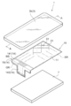
- FIG. 1 is an exploded perspective view illustrating an electronic apparatus to which the input device according to this embodiment is applied.
- 2 is a cross-sectional view taken along line AA in FIG.
- the electronic device 1 has a housing 3.
- the housing 3 is configured by a combination of a main body case portion 3a and a panel portion 3b.
- the main body case portion 3a is represented by a broken line only in FIG.
- the main body case 3a is formed of, for example, a synthetic resin material.
- the main body case part 3a is formed in a box shape whose upper part opens.
- the panel part 3b is arrange
- the panel portion 3b is formed of a translucent resin material such as glass, polycarbonate resin, or acrylic resin.
- translucent and “transparent” mean a state where the visible light transmittance is 50% or more (preferably 80% or more).
- the base material 11 which has translucency and flexibility is arrange
- a wiring board 8 to be joined to the end of the base material 11 is housed in the housing 3.
- the wiring board 8 is a flexible wiring board, for example.
- a display panel 7 such as a liquid crystal display panel or an electroluminescence display panel is accommodated in the housing 3. The display image of the display panel 7 is visible from the outside through the base material 11 and the panel portion 3b.
- the substrate 11 is formed of a light-transmitting resin film such as a flexible PET (polyethylene terephthalate) film or PC (polycarbonate) film.
- the substrate 11 may include an optical adjustment layer (such as SiO 2 ) or a hard coat layer provided on the surface of a PET film or the like.
- a plurality of first electrode portions 21 and a plurality of second electrode portions 31 are formed on the surface of the substrate 11.
- the plurality of first electrode portions 21 are regularly arranged in the first direction in the detection region SR on the base material 11.
- the plurality of second electrode portions 31 are regularly arranged in the second direction intersecting the first direction in the detection region SR on the base material 11.
- the first direction and the second direction are orthogonal to each other.
- the base material 11 is provided with a plurality of lead wires 14 that are electrically connected to the first electrode portion 21 and the second electrode portion 31.
- the lead wiring 14 extends from the detection region SR of the base material 11 to the peripheral region OR outside the detection region SR.
- the capacitance type input device 10 includes the base material 11, the first electrode portion 21, the second electrode portion 31, and the lead-out wiring 14. Details of the first electrode portion 21, the second electrode portion 31, and the lead-out wiring 14 will be described later.
- a bent portion BR is provided in the peripheral region OR of the base material 11.
- the lead-out wiring 14 includes a first wiring portion 141 provided on the detection region SR side with respect to the bent portion BR, a second wiring portion 142 provided on the opposite side of the detection region SR with respect to the bent portion BR,
- the flexible laminated body 15 is provided between the wiring part 141 and the second wiring part 142 and provided on the bent part BR.
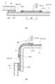
- FIG. 3A and 3B are schematic cross-sectional views illustrating the flexible laminate 15.
- FIG. 3A shows a state where the substrate 11 is not bent
- FIG. 3B shows a state where the substrate 11 is bent.
- a flexible conductive member is provided on the bent portion BR.
- a flexible laminate 15 is provided as an example of a flexible conductive member.
- the flexible laminate 15 is provided on the first amorphous ITO layer 151 provided on the substrate 11, the conductive layer 152 provided on the first amorphous ITO layer 151, and the conductive layer 152. And a second amorphous ITO layer 153.
- the first amorphous ITO layer 151 has a portion in contact with the substrate 11. Thereby, the tolerance with respect to the bending of the flexible laminated body 15 can be improved more stably.
- a conductive material having a specific resistance lower than that of the first amorphous ITO layer 151 is used for the conductive layer 152.
- a noble metal such as Au, Ag, Cu, Pt, or Pd, Ni, or an alloy containing at least one of these (a specific example is a CuNi alloy) is used.
- Au is used as the conductive layer 152.
- the conductive layer 152 may have a stacked structure.
- the second amorphous ITO layer 153 is provided on the conductive layer 152 and thereby serves to prevent the conductive layer 152 from being visually recognized from the outside.
- a connecting portion 141 a is provided at the end of the first wiring portion 141, and a connecting portion 142 a is provided at the end of the second wiring portion 142. Both ends of the flexible laminate 15 are connected to these connecting portions 141a and 142a.
- a metal layer 142c is provided on the end 142b of the second wiring part 142 opposite to the connection part 142a. The metal layer 142 c constitutes a part of a terminal portion connected to the metal terminal 8 a provided on the wiring board 8.
- the surfaces of the connecting portions 141a and 142a facing the flexible laminate 15 are preferably provided with a crystallized ITO surface, more preferably a crystallized ITO surface. Thereby, the adhesiveness (connection strength) of the 1st amorphous ITO layer 151 of the flexible laminated body 15 and the connection parts 141a and 142a improves.
- the first wiring part 141 of the lead-out wiring 14 may include a crystallized ITO layer. Further, the second wiring portion 142 of the lead-out wiring 14 may also include a crystallized ITO layer. Thereby, the translucency of the first wiring part 141 and the second wiring part 142 can be improved and the resistance can be lowered, and the crystal can be formed in the same process as the formation of the first wiring part 141 and the second wiring part 142.
- the connecting portions 141a and 142a made of the ITO layer can be formed.
- the first wiring part 141 is formed of crystallized ITO.
- the second wiring part 142 is formed of crystallized ITO on the connection part 142a side, and the end part 142b side opposite to the connection part 142a is a crystallized ITO layer and a metal layer 142c (for example, CuNi / Cu) formed thereon. / CuNi laminated structure).
- the flexible laminate 15 has a laminated structure of the first amorphous ITO layer 151, the conductive layer 152, and the second amorphous ITO layer 153, so that transparency and flexibility due to the amorphous ITO and low resistance due to the conductive layer 152 are achieved. It is possible to achieve compatibility with For example, even when the radius of curvature of the bent portion BR of the substrate 11 is 5 mm or less, sufficient resistance to mechanical breakage and electrical cutting can be obtained. That is, by providing the flexible laminated body 15 in the bent portion BR, the base material 11 can be bent while maintaining the translucency and conductivity.
- the flexible laminate 15 provided in the bent portion BR bends as the base material 11 is deformed in the bent portion BR. At this time, tensile stress is remarkably generated in the flexible laminate 15 on the side opposite to the side facing the substrate 11. This tensile stress can cause cracks in the flexible laminate 15.
- FIG. 4 is a schematic cross-sectional view illustrating a covering material.
- a covering material 51 is provided so as to cover at least a part of a flexible laminate (an example of a flexible conductive member) 15 that is bent on the bent portion BR. This makes it difficult for tensile stress to occur in the flexible laminate 15. Therefore, the provision of the covering material 51 can reduce the possibility that the flexible laminate 15 will crack.
- the covering material 51 may be provided so as to cover the entire flexible laminate 15, or a portion covering the first wiring portion 141 and the second wiring portion 142 connected to the flexible laminate 15. You may have.
- the material constituting the covering material 51 is not limited.
- An example is a resin material.
- a specific example of the resin material constituting the resin material is an epoxy resin.
- the resin material may contain an inorganic material such as silica filler or alumina filler.
- FIG. 5 is a schematic plan view illustrating the optical adhesive layer.
- 6 is a cross-sectional view taken along the line II of FIG.
- FIG. 7 is a schematic plan view illustrating a covering material in the case where an optical adhesive layer is provided.
- 8 is a cross-sectional view taken along the line II-II in FIG.
- FIG. 9 is a schematic plan view illustrating the covering material and the notch when the optical adhesive layer is provided.
- 10 is a cross-sectional view taken along line III-III in FIG.
- FIG. 11 is a schematic plan view illustrating a reinforcing member.
- An optical adhesive layer 52 made of a highly transparent adhesive is located between the substrate 11 and the panel portion 3b (3), and the substrate 11 and the panel portion are formed by the adhesiveness and cohesive force of the highly transparent adhesive. The relative position with respect to 3b (3) is maintained.
- the optical adhesive layer 52 extends from the detection region SR to the peripheral region OR side, and as shown in FIGS. 5 and 6, the highly transparent layer 15 also forms the optical adhesive layer 52.
- An adhesive may be attached. In such a case, when the bent portion BR is bent, a position change is generated such that the flexible laminate 15 and the panel portion 3b (3) are separated from each other along with the bending.
- the highly transparent pressure-sensitive adhesive constituting the optical pressure-sensitive adhesive layer 52 located between the flexible laminate 15 and the panel portion 3b (3) has a cohesive force CF in a direction to return this position change.
- the cohesive force CF acts as a tensile force on the flexible laminate 15 that deforms along the bending at the bent portion BR. Therefore, as shown in FIG. 5 and FIG. 6, when the highly transparent adhesive constituting the optical adhesive layer 52 is attached to the flexible laminate 15, the cohesive force of the highly transparent adhesive is increased. The resulting tensile stress is likely to occur in the flexible laminate 15.
- a laminated structure of the flexible laminated body 15, which is an example of the flexible conductive member, the covering material 51, and the optical adhesive layer 52 is formed. Since the covering material 51 is positioned between the optical adhesive layer 52 and the flexible laminate 15, the tensile force based on the cohesive force CF of the highly transparent adhesive constituting the optical adhesive layer 52 is first applied to the covering material. 51. For example, the tensile force from the highly transparent pressure-sensitive adhesive constituting the optical pressure-sensitive adhesive layer 52 is relaxed by the cohesive force of the resin-based material constituting the coating material inside the coating material 51. For this reason, it can suppress that the tensile force from the highly transparent adhesive which comprises the optical adhesive layer 52 is transmitted to the flexible laminated body 15.
- a cutout portion 52 ⁇ / b> C may be provided in part of the optical adhesive layer 52 so that the highly transparent adhesive constituting the optical adhesive layer 52 does not cover the bent portion of the flexible laminate 15.
- the bending portion BR may be further provided with a reinforcing member that reduces the degree of bending of the flexible laminate 15 which is an example of the flexible conductive member.
- FIG. 11 shows a reinforcing film 50 provided on the side opposite to the side where the flexible laminate 15 is provided in the bent portion BR.
- the reinforcing film 50 include translucent resin films such as a PET (polyethylene terephthalate) film and a PC (polycarbonate) film.
- the reinforcing film 50 may be preferably composed of a film having lower flexibility (higher rigidity) than a film constituting the base material 11 positioned at the bent portion BR.
- FIG. 12 is a schematic plan view showing the arrangement of electrodes.
- FIGS. 13A and 13B are schematic cross-sectional views of the bridge wiring portion.
- the base material 11 includes a first electrode row 20 extending in the first direction (Y direction) on the surface of the base material 11, and a second electrode row 30 extending in the second direction (X direction). Is formed.
- a plurality of first electrode portions 21 and a connecting portion 22 that connects the first electrode portions 21 in the Y direction are integrally formed.
- the first electrode rows 20 are provided in three rows, y1, y2, and y3, and this number is selected according to the area of the input device 10.
- the first electrode portion 21 is substantially square (or substantially rhombus), and the corners of the substantially square are directed in the X direction and the Y direction.
- the connecting portion 22 connects the corner portions of the first electrode portions 21 adjacent in the Y direction.
- the second electrode rows 30 are regularly arranged along the four rows x1, x2, x3, and x4 at an equal pitch in the X direction, and along each row of ya, yb, yc, and yd. They are regularly arranged in the Y direction at an equal pitch.
- the number of columns in the X direction and the Y direction is selected according to the area of the input device 10.
- the 2nd electrode part 31 is a substantially square (or substantially rhombus), and each corner
- the sizes of the square sides of the first electrode portion 21 and the second electrode portion 31 are substantially the same.
- Some of the second electrode portions 31 have a wiring passage 32 formed at the center thereof.
- the second electrode portion in which the wiring passage 32 is formed is denoted by reference numeral 31 ⁇ / b> A to distinguish it from the second electrode portion 31 that does not have the wiring passage 32.
- the wiring passage 32 is formed to extend linearly in the Y direction.
- the wiring passage 32 is formed in the central portion in the X direction so that the second electrode portion 31A can be evenly divided in the X direction.
- the second electrode portion 31 ⁇ / b> A is divided into two segmented electrode layers 33 and 33 by the wiring passage 32.
- the first electrode portion 21, the connecting portion 22, and the second electrode portions 31, 31A are formed of the same light-transmitting conductive material.
- the light-transmitting conductive material is ITO, metal nanowires typified by silver nanowires, thin metal formed in a mesh shape, or conductive polymer.
- FIG. 13 (a) shows a cross-sectional view of the laminated structure of the intersection (BB line) between the first electrode row 20 in the y1 row and the second electrode row 30 in the x2 row in FIG.
- a translucent first insulating layer 41 that covers the connecting portion 22 of the first electrode array 20 is formed.
- a first bridge connection layer 42 is formed on the first insulating layer 41. By the first bridge connection layer 42, the second electrode portions 31 adjacent on both sides in the X direction of the connecting portion 22 are connected and conducted.
- the first insulating layer 41 and the first bridge connection layer 42 are formed at all the intersections of the first electrode row 20 and the second electrode row 30, and the second electrode portions 31 and 31A arranged in the x1 row. Are connected in the X direction. Similarly, in the x2, x3, and x4 columns, the second electrode portions 31 and 31A are connected in the X direction.
- the translucent first insulating layer 41 is composed of a novolac resin or a novolac resin and an acrylic resin.
- the first bridge connection layer 42 has the same layer structure as the flexible laminate 15. That is, the first bridge connection layer 42 has a laminated structure of the first amorphous ITO layer 151, the conductive layer 152, and the second amorphous ITO layer 153.
- the 1st electrode part 21, the connection part 22, and the 2nd electrode part 31 are formed with an ITO layer, by forming these with crystallized ITO, the 1st electrode part 21, the connection part 22, and the 2nd electrode It is possible to select and etch the crystallized ITO layer constituting the portion 31 and the material constituting the first insulating layer 41.
- the first wiring portion 141 and the second wiring portion 142 are connected to the flexible laminated body 141, the surfaces of the connecting portions 141a and 142a facing the flexible laminated body 15 are preferably made of crystallized ITO.
- the first electrode part 21, the connecting part 22 and the second electrode part 31 are made of crystallized ITO, so that the first electrode part 21, the connecting part 22, the second electrode part 31, the first wiring part 141 and the second electrode part 2 are formed.
- the part including the connection parts 141a and 142a of the wiring part 142 can be integrally formed of crystallized ITO.
- a connecting portion that connects the second electrode portions 31 and 31A adjacent in the X direction is formed integrally with the second electrode portions 31 and 31A.
- the plurality of second electrode portions 31 and 31A may be formed continuously in the X direction.
- the first electrode portions 21 that are independent from each other are disposed on both sides in the Y direction across the connecting portion, and the first insulating layer 41 and the first insulating layer 41 are disposed on the connecting portion that connects the second electrode portions 31 and 31A.
- One bridge connection layer 42 is formed, and the first bridge connection layer 42 connects the first electrode portions 21 adjacent in the Y direction.
- the first wiring layer 25a formed integrally with the first electrode portion 21 in the y1 row, and the y2 and y3 rows First wiring layers 25b and 25c formed integrally with each of the first electrode portions 21 are formed.
- second wiring layers 35a, 35b, 35c, and 35d that are electrically connected to the second electrode rows 30 are formed.
- Each of the first wiring layers 25a, 25b, 25c and the second wiring layers 35a, 35b, 35c, 35d is a lead-out wiring 14.
- the first wiring layers 25a, 25b, and 25c and the second wiring layers 35a, 35b, 35c, and 35d are routed in the peripheral region OR, and are electrically connected to the metal layer 142c of the second wiring portion 142 provided in the peripheral region OR. ing.
- the second wiring layer 35a is formed integrally with the second electrode portion 31 located at the intersection of the x1 row and the ya row.
- the second wiring layer 35b is formed integrally with the second electrode portion 31 located at the intersection of the x2 column and the yb column.
- the second wiring layer 35b passes through the inside of the wiring passage 32 formed in the second electrode portion 31A located at the intersection of the x1 column and the yb column, linearly extends in the Y direction, and reaches the peripheral region OR. Yes.
- the second wiring layer 35c is formed integrally with the second electrode portion 31 located at the intersection of the x3 row and the yc row.
- the second wiring layer 35c is connected to the wiring path 32 formed in the second electrode portion 31A located at the intersection of the x2 row and the yc row and the second electrode portion 31A located at the intersection of the x1 row and the yc row. It passes through the formed wiring passage 32 and extends linearly in the Y direction to the peripheral region OR.
- the second wiring layer 35d is formed integrally with the second electrode portion 31 located at the intersection of the x4 column and the yd column.
- the second wiring layer 35d is connected to the wiring path 32 formed in the second electrode portion 31A located at the intersection of the x3 row and the yd row and the second electrode portion 31A located at the intersection of the x2 row and the yd row. Passes through the formed wiring passage 32 and the wiring passage 32 formed in the second electrode portion 31A located at the intersection of the x1 row and the yd row, and linearly extends in the Y direction to reach the peripheral region OR. Yes.
- the second wiring layer 35a is electrically connected to the second electrode portions 31 and 31A constituting the second electrode row 30 located in the x1 row, and the second wiring layers 35b, 35c and 35d are x2, x3 and x4. Each of the second electrode portions 31 and 31A constituting the second electrode row 30 located in the row is electrically connected.
- the second wiring layers 35 a, 35 b, 35 c, and 35 d are all formed integrally with the second electrode portion 31 by a translucent conductive material that constitutes the second electrode portion 31.
- FIG. 13B is a cross-sectional view of the laminated structure of the intersection (CC line) between the first electrode row 20 in the x3 row and the second electrode row 30 in the yd row in FIG.
- the second electrode portion 31 ⁇ / b> A is divided into two divided electrode layers 33 and 33 by the wiring passage 32.
- a second insulating layer 43 is formed on the wiring path 32 and the second wiring layer 35d, and a second bridge connection layer 44 is formed thereon.
- the divided electrode layers 33 and 33 divided by the wiring passage 32 are connected by the second bridge connection layer 44, whereby the entire second electrode portion 31A can function as one electrode layer. This is the same in all of the second electrode portions 31A provided in other places.
- the second insulating layer 43 shown in FIG. 13B is formed of the same material and in the same process as the first insulating layer 41 shown in FIG.
- the second bridge connection layer 44 shown in FIG. 13B is formed of the same material and in the same process as the first bridge connection layer 42 shown in FIG.
- a material in which a layer made of a light-transmitting conductive material such as ITO is provided on the surface of the base material 11 is used.
- a preferred translucent conductive material is crystallized ITO.
- a resin layer of novolac resin and acrylic resin is formed on the substrate 11, and the first insulating layer 41 and the second insulating layer 43 are simultaneously patterned in a photolithography process. Further, a laminated body for the bridge connection layer is formed, and the first bridge connection layer 42 and the second bridge connection layer 44 are simultaneously formed by an etching process. The laminated body for the bridge connection layer is also formed in the peripheral region OR. Then, it is possible to connect the connection part 141a of the first wiring part 141 and the connection part 142a of the second wiring part 142 in the same process as the process of forming the first bridge connection layer 42 and the second bridge connection layer 44 by etching. A flexible laminate 15 is formed.
- the display image of the display panel 7 can be visually observed from the outside through the input device 10 and the panel unit 3b.
- the input device 10 can be operated by touching the panel unit 3b with a finger while viewing this display.
- a capacitance is formed between the first electrode row 20 and the second electrode row 30.
- One of the first electrode array 20 and the second electrode array 30 is sequentially supplied with pulsed drive power, and when the drive power is applied, a detection current flowing through the other electrode array is detected. .
- a capacitance is formed between the finger and the electrode layer.
- the detection current changes. By detecting this change in the detected current, it is possible to detect which part of the panel portion 3b the finger is approaching.
- the area is substantially smaller than that of the electrode section that does not have the wiring path 32, and the sensitivity for each electrode layer in the detection operation. May vary. Therefore, an opening 31b is formed in the second electrode portion 31 where the wiring passage 32 is not formed, and the second electrode portion 31A including the wiring passage 32 and the second electrode portion 31 not including the wiring passage 32 are formed. The difference of the area is made not so much.
- an opening 21b is also formed in the first electrode portion 21, so that the difference in area between the first electrode portion 21 and the second electrode portion 31A is not greatly different.
- the second wiring layers 35a, 35b, 35c, and 35d extend in the Y direction through the inside of the wiring passage 32 formed in the second electrode portion 31A. Since the second wiring layers 35b, 35c, and 35d are narrowed by the partition electrode layers 33 and 33 of the second electrode portion 31A on both sides in the X direction, the second wiring layers 35b, 35c, and 35d, and the first electrode portion The area adjacent to 21 can be reduced. Thereby, the electrostatic coupling between the second wiring layers 35b, 35c, 35d and the first electrode portion 21 can be reduced.
- the second wiring layers 35b, 35c, and 35d pass through the inside of the second electrode portion 31A, it is not necessary to form a passage for passing the second wiring layer between the adjacent electrode layers. . Therefore, the arrangement of the first electrode portion 21 and the second electrode portion 31 is not restricted due to the routing of the second wiring layer.
- the first electrode part 21 and the second electrode part 31 can be arranged close to each other, and the resolution of the detection operation can be increased.
- an input device that can bend a wiring together with a base material without impairing translucency and conductivity.
Landscapes
- Engineering & Computer Science (AREA)
- General Engineering & Computer Science (AREA)
- Theoretical Computer Science (AREA)
- Human Computer Interaction (AREA)
- Physics & Mathematics (AREA)
- General Physics & Mathematics (AREA)
- Computer Networks & Wireless Communication (AREA)
- Position Input By Displaying (AREA)
Abstract
Description
図1は、本実施形態に係る入力装置が適用された電子機器を例示する分解斜視図である。
図2は、図1のA-A線断面図である。
図1および図2に示すように、電子機器1は筐体3を有している。筐体3は、本体ケース部3aと、パネル部3bとの組み合わせによって構成される。なお、説明の都合上、本体ケース部3aは図2のみに破線で表される。本体ケース部3aは、例えば合成樹脂材料で形成される。本体ケース部3aは、上方が開口する箱形状に形成される。パネル部3bは、本体ケース部3aの開口部を覆うように配置される。
図3(a)には基材11が屈曲していない状態が示され、図3(b)には基材11が屈曲している状態が示される。
屈曲部BRの上には、可撓性導電部材が設けられる。図3に示される入力装置では、可撓性導電部材の一例として可撓性積層体15が設けられている。可撓性積層体15は、基材11の上に設けられた第1アモルファスITO層151と、第1アモルファスITO層151の上に設けられた導電層152と、導電層152の上に設けられた第2アモルファスITO層153とを有する。
次に、第1電極部21、第2電極部31および引き出し配線14の詳細について説明する。
図12は、電極の配置を示す模式平面図である。
図13(a)および(b)はブリッジ配線部分の模式断面図である。
図12に示すように、基材11には、基材11の表面における第1方向(Y方向)に延びる第1電極列20と、第2方向(X方向)に延びる第2電極列30とが形成される。第1電極列20では、複数の第1電極部21と、第1電極部21をY方向に連結する連結部22とが一体に形成される。第1電極列20は、y1,y2,y3の3列設けられている
が、この数は入力装置10の面積に応じて選択される。
3…筐体
3a…本体ケース部
3b…パネル部
7…表示パネル
8…配線基板
8a…金属端子
10…入力装置
11…基材
14…引き出し配線
15…可撓性積層体
20…第1電極列
21…第1電極部
21b…開口部
22…連結部
25a,25b,25c…第1配線層
30…第2電極列
31…第2電極部
31A…第2電極部
31b…開口部
32…配線通路
33…区分電極層
35a,35b,35c,35d…第2配線層
41…第1絶縁層
42…第1ブリッジ接続層
43…第2絶縁層
44…第2ブリッジ接続層
50…補強フィルム
51…被覆材
52…光学粘着剤層
52C…切欠部
141…第1配線部
141a,142a…接続部
142…第2配線部
142b…端部
142c…金属層
152…導電層
BR…屈曲部
151…第1アモルファスITO層
153…第2アモルファスITO層
OR…周辺領域
SR…検出領域
CF…凝集力
Claims (9)
- 透光性および可撓性を有する基材と、
透光性を有し、前記基材の上の検出領域において第1方向に並ぶ複数の第1電極部と、
透光性を有し、前記基材の上の前記検出領域において前記第1方向と交差する第2方向に並ぶ複数の第2電極部と、
前記複数の第1電極部および前記複数の第2電極部のそれぞれと導通し、前記基材の上の前記検出領域から前記検出領域の外側の周辺領域まで延在する複数の引き出し配線とを備え、
前記基材の前記周辺領域には屈曲部が設けられ、
前記引き出し配線は、前記屈曲部の上に設けられた可撓性導電部材を有し、
前記屈曲部の上に設けられた前記可撓性導電部材の少なくとも一部を覆うように設けられた被覆材を備えること
を特徴とする入力装置。 - 前記被覆材は樹脂系材料からなる、請求項1に記載の入力装置。
- 前記可撓性導電部材の屈曲の程度を低減する補強部材をさらに備える、請求項1または請求項2に記載の入力装置。
- 前記補強部材は、前記屈曲部における前記可撓性導電部材が設けられた側とは反対側に設けられた補強フィルムからなる、請求項3に記載の入力装置。
- 前記基材の上の前記検出領域を覆うように設けられた光学粘着剤層をさらに備える、請求項1から請求項4のいずれか一項に記載の入力装置。
- 前記可撓性導電部材、前記被覆材および前記光学粘着剤層の積層構造が形成されるように、前記光学粘着剤層は前記検出領域から前記周辺領域側に延出する、請求項5に記載の入力装置。
- 前記光学粘着剤層は、前記検出領域から前記周辺領域側に延出するが、前記可撓性導電部材における屈曲した状態にある部分を覆わないように配置される、請求項5に記載の入力装置。
- 前記引き出し配線は、前記屈曲部よりも前記検出領域側に設けられた第1配線部と、前記屈曲部よりも前記検出領域とは反対側に設けられた第2配線部と、を有し、
前記可撓性積層体は、前記第1配線部と前記第2配線部との間に位置する、請求項1から請求項7のいずれか一項に記載の入力装置。 - 前記可撓性導電部材は、前記基材の上に設けられた第1アモルファスITO層と、前記第1アモルファスITO層の上に設けられた導電層と、前記導電層の上に設けられた第2アモルファスITO層とを有する可撓性積層体からなる、請求項1から請求項8のいずれか一項に記載の入力装置。
Priority Applications (5)
| Application Number | Priority Date | Filing Date | Title |
|---|---|---|---|
| JP2018516365A JP6630433B2 (ja) | 2016-05-12 | 2017-03-09 | 入力装置 |
| EP17795812.1A EP3457259B1 (en) | 2016-05-12 | 2017-03-09 | Input device |
| CN201780029300.4A CN109154871B (zh) | 2016-05-12 | 2017-03-09 | 输入装置 |
| KR1020187032473A KR102243967B1 (ko) | 2016-05-12 | 2017-03-09 | 입력 장치 |
| US16/155,599 US10761663B2 (en) | 2016-05-12 | 2018-10-09 | Input device |
Applications Claiming Priority (2)
| Application Number | Priority Date | Filing Date | Title |
|---|---|---|---|
| JP2016-095858 | 2016-05-12 | ||
| JP2016095858 | 2016-05-12 |
Related Child Applications (1)
| Application Number | Title | Priority Date | Filing Date |
|---|---|---|---|
| US16/155,599 Continuation US10761663B2 (en) | 2016-05-12 | 2018-10-09 | Input device |
Publications (1)
| Publication Number | Publication Date |
|---|---|
| WO2017195451A1 true WO2017195451A1 (ja) | 2017-11-16 |
Family
ID=60266411
Family Applications (1)
| Application Number | Title | Priority Date | Filing Date |
|---|---|---|---|
| PCT/JP2017/009397 Ceased WO2017195451A1 (ja) | 2016-05-12 | 2017-03-09 | 入力装置 |
Country Status (7)
| Country | Link |
|---|---|
| US (1) | US10761663B2 (ja) |
| EP (1) | EP3457259B1 (ja) |
| JP (1) | JP6630433B2 (ja) |
| KR (1) | KR102243967B1 (ja) |
| CN (1) | CN109154871B (ja) |
| TW (2) | TWI656464B (ja) |
| WO (1) | WO2017195451A1 (ja) |
Cited By (8)
| Publication number | Priority date | Publication date | Assignee | Title |
|---|---|---|---|---|
| CN110943092A (zh) * | 2018-09-21 | 2020-03-31 | 三星显示有限公司 | 显示装置 |
| KR20200090868A (ko) | 2018-01-22 | 2020-07-29 | 알프스 알파인 가부시키가이샤 | 입력 장치 |
| WO2020261662A1 (ja) * | 2019-06-25 | 2020-12-30 | アルプスアルパイン株式会社 | 入力装置および入力装置付き表示装置 |
| JP2021511650A (ja) * | 2018-01-30 | 2021-05-06 | 京東方科技集團股▲ふん▼有限公司Boe Technology Group Co.,Ltd. | 電子基板及びその製造方法、電子装置 |
| WO2021149409A1 (ja) * | 2020-01-20 | 2021-07-29 | アルプスアルパイン株式会社 | 入力装置 |
| US11296157B2 (en) | 2018-11-09 | 2022-04-05 | Lg Display Co., Ltd. | Display device |
| CN115985191A (zh) * | 2018-05-15 | 2023-04-18 | 三星显示有限公司 | 可折叠显示装置 |
| JP2025010011A (ja) * | 2023-06-28 | 2025-01-20 | エルジー ディスプレイ カンパニー リミテッド | 表示装置及び表示パネル |
Families Citing this family (3)
| Publication number | Priority date | Publication date | Assignee | Title |
|---|---|---|---|---|
| CN112244810A (zh) * | 2020-04-16 | 2021-01-22 | 广东乐心医疗电子股份有限公司 | 体脂检测器 |
| TWI825990B (zh) | 2022-09-14 | 2023-12-11 | 元太科技工業股份有限公司 | 觸控顯示裝置 |
| CN115359726B (zh) * | 2022-09-21 | 2023-07-21 | 武汉天马微电子有限公司 | 一种四曲面柔性显示装置 |
Citations (3)
| Publication number | Priority date | Publication date | Assignee | Title |
|---|---|---|---|---|
| JP2010165094A (ja) * | 2009-01-14 | 2010-07-29 | Fujikura Ltd | 静電容量式タッチセンサ |
| JP2015028211A (ja) * | 2013-06-26 | 2015-02-12 | 株式会社神戸製鋼所 | 反射膜用または配線電極用Ag合金膜、反射膜または配線電極、および反射膜用または配線電極用Ag合金スパッタリングターゲット |
| WO2015147323A1 (ja) * | 2014-03-28 | 2015-10-01 | ポリマテック・ジャパン株式会社 | タッチセンサ |
Family Cites Families (24)
| Publication number | Priority date | Publication date | Assignee | Title |
|---|---|---|---|---|
| EP2134415B1 (en) * | 2007-03-08 | 2017-05-03 | Second Sight Medical Products, Inc. | Flexible circuit electrode array |
| CN101923412A (zh) * | 2009-06-16 | 2010-12-22 | 时纬科技股份有限公司 | 触摸屏及其制造方法 |
| JP5611864B2 (ja) * | 2011-03-09 | 2014-10-22 | アルプス電気株式会社 | 入力装置及び入力装置の製造方法 |
| KR20130008876A (ko) * | 2011-07-13 | 2013-01-23 | 삼성전기주식회사 | 터치패널의 제조방법 |
| US8546925B2 (en) * | 2011-09-28 | 2013-10-01 | Texas Instruments Incorporated | Synchronous buck converter having coplanar array of contact bumps of equal volume |
| CN103246385B (zh) * | 2012-02-10 | 2016-05-25 | 阿尔卑斯电气株式会社 | 输入装置 |
| JP2013186633A (ja) | 2012-03-07 | 2013-09-19 | Toppan Printing Co Ltd | 透明導電膜、透明導電膜製造方法およびタッチパネル |
| US9120187B2 (en) * | 2012-06-08 | 2015-09-01 | Nokia Technologies Oy | Multilayer 3D glass window with embedded functions |
| WO2014080467A1 (ja) * | 2012-11-21 | 2014-05-30 | 東海ゴム工業株式会社 | 荷重センサ |
| CN104063020A (zh) * | 2013-08-13 | 2014-09-24 | 钟钢 | 多功能人机交互系统及其通讯方法 |
| CN104423715B (zh) | 2013-09-11 | 2019-07-23 | Lg伊诺特有限公司 | 触摸窗和包括该触摸窗的显示器 |
| JP2015069267A (ja) * | 2013-09-27 | 2015-04-13 | デクセリアルズ株式会社 | 静電容量型曲面形状タッチパネル及びその製造方法 |
| KR102307432B1 (ko) * | 2013-12-09 | 2021-09-30 | 삼성디스플레이 주식회사 | 표시 장치 |
| US9516744B2 (en) * | 2014-04-16 | 2016-12-06 | Eastman Kodak Company | Wrap-around micro-wire circuit method |
| KR102351666B1 (ko) * | 2014-07-14 | 2022-01-14 | 삼성디스플레이 주식회사 | 터치 패널을 구비한 플랙서블 표시 장치 |
| US10394350B2 (en) * | 2014-08-11 | 2019-08-27 | Atmel Corporation | Fabricated electrical circuit on touch sensor substrate |
| TWM495566U (zh) * | 2014-08-19 | 2015-02-11 | Hannstouch Solution Inc | 觸控面板 |
| KR102305398B1 (ko) * | 2014-09-03 | 2021-09-28 | 삼성디스플레이 주식회사 | 표시장치 |
| KR20160050146A (ko) * | 2014-10-28 | 2016-05-11 | 삼성디스플레이 주식회사 | 표시 장치 |
| CN104700813B (zh) * | 2015-04-01 | 2017-10-03 | 上海中航光电子有限公司 | 阵列基板及其形成方法 |
| CN104765499A (zh) * | 2015-04-15 | 2015-07-08 | 合肥京东方光电科技有限公司 | 触摸屏及触控装置 |
| CN204576461U (zh) * | 2015-04-24 | 2015-08-19 | 南昌欧菲光科技有限公司 | 触摸屏及其感应模块 |
| DE112016002887T5 (de) * | 2015-06-26 | 2018-03-08 | Alps Electric Co., Ltd. | Eingabevorrichtung |
| CN107025007B (zh) * | 2016-02-01 | 2023-10-24 | 宸鸿科技(厦门)有限公司 | 触控面板及其立体盖板 |
-
2017
- 2017-03-09 KR KR1020187032473A patent/KR102243967B1/ko not_active Expired - Fee Related
- 2017-03-09 EP EP17795812.1A patent/EP3457259B1/en active Active
- 2017-03-09 CN CN201780029300.4A patent/CN109154871B/zh not_active Expired - Fee Related
- 2017-03-09 JP JP2018516365A patent/JP6630433B2/ja not_active Expired - Fee Related
- 2017-03-09 WO PCT/JP2017/009397 patent/WO2017195451A1/ja not_active Ceased
- 2017-05-09 TW TW107107043A patent/TWI656464B/zh not_active IP Right Cessation
- 2017-05-09 TW TW106115236A patent/TWI624776B/zh not_active IP Right Cessation
-
2018
- 2018-10-09 US US16/155,599 patent/US10761663B2/en not_active Expired - Fee Related
Patent Citations (3)
| Publication number | Priority date | Publication date | Assignee | Title |
|---|---|---|---|---|
| JP2010165094A (ja) * | 2009-01-14 | 2010-07-29 | Fujikura Ltd | 静電容量式タッチセンサ |
| JP2015028211A (ja) * | 2013-06-26 | 2015-02-12 | 株式会社神戸製鋼所 | 反射膜用または配線電極用Ag合金膜、反射膜または配線電極、および反射膜用または配線電極用Ag合金スパッタリングターゲット |
| WO2015147323A1 (ja) * | 2014-03-28 | 2015-10-01 | ポリマテック・ジャパン株式会社 | タッチセンサ |
Cited By (15)
| Publication number | Priority date | Publication date | Assignee | Title |
|---|---|---|---|---|
| KR20200090868A (ko) | 2018-01-22 | 2020-07-29 | 알프스 알파인 가부시키가이샤 | 입력 장치 |
| JP7592388B2 (ja) | 2018-01-30 | 2024-12-02 | 京東方科技集團股▲ふん▼有限公司 | 電子基板及びその製造方法、電子装置 |
| JP2021511650A (ja) * | 2018-01-30 | 2021-05-06 | 京東方科技集團股▲ふん▼有限公司Boe Technology Group Co.,Ltd. | 電子基板及びその製造方法、電子装置 |
| CN115985191A (zh) * | 2018-05-15 | 2023-04-18 | 三星显示有限公司 | 可折叠显示装置 |
| CN110943092A (zh) * | 2018-09-21 | 2020-03-31 | 三星显示有限公司 | 显示装置 |
| US11296157B2 (en) | 2018-11-09 | 2022-04-05 | Lg Display Co., Ltd. | Display device |
| US11610946B2 (en) | 2018-11-09 | 2023-03-21 | Lg Display Co., Ltd. | Display device |
| EP3651001B1 (en) * | 2018-11-09 | 2023-12-06 | LG Display Co., Ltd. | Display device |
| US11985884B2 (en) | 2018-11-09 | 2024-05-14 | Lg Display Co., Ltd. | Display device |
| WO2020261662A1 (ja) * | 2019-06-25 | 2020-12-30 | アルプスアルパイン株式会社 | 入力装置および入力装置付き表示装置 |
| JPWO2021149409A1 (ja) * | 2020-01-20 | 2021-07-29 | ||
| WO2021149409A1 (ja) * | 2020-01-20 | 2021-07-29 | アルプスアルパイン株式会社 | 入力装置 |
| JP7426416B2 (ja) | 2020-01-20 | 2024-02-01 | アルプスアルパイン株式会社 | 入力装置 |
| JP2025010011A (ja) * | 2023-06-28 | 2025-01-20 | エルジー ディスプレイ カンパニー リミテッド | 表示装置及び表示パネル |
| JP7686123B2 (ja) | 2023-06-28 | 2025-05-30 | エルジー ディスプレイ カンパニー リミテッド | 表示装置及び表示パネル |
Also Published As
| Publication number | Publication date |
|---|---|
| TWI624776B (zh) | 2018-05-21 |
| CN109154871B (zh) | 2021-10-22 |
| JP6630433B2 (ja) | 2020-01-15 |
| CN109154871A (zh) | 2019-01-04 |
| TW201820097A (zh) | 2018-06-01 |
| EP3457259A1 (en) | 2019-03-20 |
| US10761663B2 (en) | 2020-09-01 |
| TW201740258A (zh) | 2017-11-16 |
| KR20180126596A (ko) | 2018-11-27 |
| EP3457259B1 (en) | 2021-07-21 |
| EP3457259A4 (en) | 2019-11-27 |
| KR102243967B1 (ko) | 2021-04-26 |
| JPWO2017195451A1 (ja) | 2019-01-10 |
| US20190050083A1 (en) | 2019-02-14 |
| TWI656464B (zh) | 2019-04-11 |
Similar Documents
| Publication | Publication Date | Title |
|---|---|---|
| JP6630433B2 (ja) | 入力装置 | |
| KR102373330B1 (ko) | 터치 센서를 포함하는 표시 장치 및 그 제조 방법 | |
| JP6625355B2 (ja) | タッチパネルを備えるフレキシブル表示装置 | |
| CN105630226B (zh) | 触摸窗 | |
| KR102281850B1 (ko) | 터치 센서, 그 제조 방법 및 이를 포함하는 표시 장치 | |
| TW201610783A (zh) | 層疊構造體、觸摸面板、帶觸摸面板的顯示裝置及其製造方法 | |
| KR20160086499A (ko) | 플렉서블 터치 패널 및 플렉서블 표시 장치 | |
| KR102367249B1 (ko) | 플렉서블 터치 패널 및 플렉서블 터치 패널의 제조 방법 | |
| CN107636579B (zh) | 输入装置 | |
| US9880683B2 (en) | Touch panel and organic light emitting diode display device | |
| TW201523367A (zh) | 觸控面板 | |
| KR20170140515A (ko) | 터치 윈도우 및 터치 디바이스 | |
| KR20160133603A (ko) | 터치 스크린 패널 | |
| KR20160095314A (ko) | 터치 스크린 패널 | |
| WO2016199263A1 (ja) | 入力装置 | |
| KR102313959B1 (ko) | 터치 윈도우 | |
| KR102199344B1 (ko) | 터치 윈도우 | |
| KR20250019230A (ko) | 입력 센서 및 이를 포함하는 표시 장치 | |
| KR102251876B1 (ko) | 터치 윈도우 | |
| KR20160073278A (ko) | 터치 센서 장치 및 이를 포함하는 표시 장치 | |
| KR20160037469A (ko) | 터치 윈도우 및 터치 디바이스 | |
| KR20170120007A (ko) | 터치 윈도우 및 터치 디바이스 |
Legal Events
| Date | Code | Title | Description |
|---|---|---|---|
| WWE | Wipo information: entry into national phase |
Ref document number: 2018516365 Country of ref document: JP |
|
| ENP | Entry into the national phase |
Ref document number: 20187032473 Country of ref document: KR Kind code of ref document: A |
|
| NENP | Non-entry into the national phase |
Ref country code: DE |
|
| 121 | Ep: the epo has been informed by wipo that ep was designated in this application |
Ref document number: 17795812 Country of ref document: EP Kind code of ref document: A1 |
|
| ENP | Entry into the national phase |
Ref document number: 2017795812 Country of ref document: EP Effective date: 20181212 |