WO2017199510A1 - 蛍光測定装置の校正用基準体 - Google Patents
蛍光測定装置の校正用基準体 Download PDFInfo
- Publication number
- WO2017199510A1 WO2017199510A1 PCT/JP2017/006774 JP2017006774W WO2017199510A1 WO 2017199510 A1 WO2017199510 A1 WO 2017199510A1 JP 2017006774 W JP2017006774 W JP 2017006774W WO 2017199510 A1 WO2017199510 A1 WO 2017199510A1
- Authority
- WO
- WIPO (PCT)
- Prior art keywords
- light
- phosphor
- fluorescence
- reference body
- layer
- Prior art date
- Legal status (The legal status is an assumption and is not a legal conclusion. Google has not performed a legal analysis and makes no representation as to the accuracy of the status listed.)
- Ceased
Links
Images


Classifications
-
- G—PHYSICS
- G01—MEASURING; TESTING
- G01N—INVESTIGATING OR ANALYSING MATERIALS BY DETERMINING THEIR CHEMICAL OR PHYSICAL PROPERTIES
- G01N21/00—Investigating or analysing materials by the use of optical means, i.e. using sub-millimetre waves, infrared, visible or ultraviolet light
- G01N21/62—Systems in which the material investigated is excited whereby it emits light or causes a change in wavelength of the incident light
- G01N21/63—Systems in which the material investigated is excited whereby it emits light or causes a change in wavelength of the incident light optically excited
- G01N21/64—Fluorescence; Phosphorescence
- G01N21/6489—Photoluminescence of semiconductors
-
- G—PHYSICS
- G01—MEASURING; TESTING
- G01N—INVESTIGATING OR ANALYSING MATERIALS BY DETERMINING THEIR CHEMICAL OR PHYSICAL PROPERTIES
- G01N21/00—Investigating or analysing materials by the use of optical means, i.e. using sub-millimetre waves, infrared, visible or ultraviolet light
- G01N21/17—Systems in which incident light is modified in accordance with the properties of the material investigated
- G01N21/25—Colour; Spectral properties, i.e. comparison of effect of material on the light at two or more different wavelengths or wavelength bands
- G01N21/27—Colour; Spectral properties, i.e. comparison of effect of material on the light at two or more different wavelengths or wavelength bands using photo-electric detection ; circuits for computing concentration
- G01N21/274—Calibration, base line adjustment, drift correction
- G01N21/278—Constitution of standards
-
- G—PHYSICS
- G01—MEASURING; TESTING
- G01N—INVESTIGATING OR ANALYSING MATERIALS BY DETERMINING THEIR CHEMICAL OR PHYSICAL PROPERTIES
- G01N21/00—Investigating or analysing materials by the use of optical means, i.e. using sub-millimetre waves, infrared, visible or ultraviolet light
- G01N21/62—Systems in which the material investigated is excited whereby it emits light or causes a change in wavelength of the incident light
- G01N21/63—Systems in which the material investigated is excited whereby it emits light or causes a change in wavelength of the incident light optically excited
- G01N21/64—Fluorescence; Phosphorescence
- G01N21/645—Specially adapted constructive features of fluorimeters
-
- G—PHYSICS
- G01—MEASURING; TESTING
- G01N—INVESTIGATING OR ANALYSING MATERIALS BY DETERMINING THEIR CHEMICAL OR PHYSICAL PROPERTIES
- G01N21/00—Investigating or analysing materials by the use of optical means, i.e. using sub-millimetre waves, infrared, visible or ultraviolet light
- G01N21/62—Systems in which the material investigated is excited whereby it emits light or causes a change in wavelength of the incident light
- G01N21/63—Systems in which the material investigated is excited whereby it emits light or causes a change in wavelength of the incident light optically excited
- G01N21/64—Fluorescence; Phosphorescence
- G01N2021/6417—Spectrofluorimetric devices
- G01N2021/6419—Excitation at two or more wavelengths
-
- G—PHYSICS
- G01—MEASURING; TESTING
- G01N—INVESTIGATING OR ANALYSING MATERIALS BY DETERMINING THEIR CHEMICAL OR PHYSICAL PROPERTIES
- G01N21/00—Investigating or analysing materials by the use of optical means, i.e. using sub-millimetre waves, infrared, visible or ultraviolet light
- G01N21/62—Systems in which the material investigated is excited whereby it emits light or causes a change in wavelength of the incident light
- G01N21/63—Systems in which the material investigated is excited whereby it emits light or causes a change in wavelength of the incident light optically excited
- G01N21/64—Fluorescence; Phosphorescence
- G01N21/645—Specially adapted constructive features of fluorimeters
- G01N2021/6463—Optics
-
- G—PHYSICS
- G01—MEASURING; TESTING
- G01N—INVESTIGATING OR ANALYSING MATERIALS BY DETERMINING THEIR CHEMICAL OR PHYSICAL PROPERTIES
- G01N21/00—Investigating or analysing materials by the use of optical means, i.e. using sub-millimetre waves, infrared, visible or ultraviolet light
- G01N21/62—Systems in which the material investigated is excited whereby it emits light or causes a change in wavelength of the incident light
- G01N21/63—Systems in which the material investigated is excited whereby it emits light or causes a change in wavelength of the incident light optically excited
- G01N21/64—Fluorescence; Phosphorescence
- G01N2021/6491—Measuring fluorescence and transmission; Correcting inner filter effect
-
- G—PHYSICS
- G01—MEASURING; TESTING
- G01N—INVESTIGATING OR ANALYSING MATERIALS BY DETERMINING THEIR CHEMICAL OR PHYSICAL PROPERTIES
- G01N21/00—Investigating or analysing materials by the use of optical means, i.e. using sub-millimetre waves, infrared, visible or ultraviolet light
- G01N21/84—Systems specially adapted for particular applications
- G01N21/8483—Investigating reagent band
- G01N2021/8488—Investigating reagent band the band presenting reference patches
-
- G—PHYSICS
- G01—MEASURING; TESTING
- G01N—INVESTIGATING OR ANALYSING MATERIALS BY DETERMINING THEIR CHEMICAL OR PHYSICAL PROPERTIES
- G01N2201/00—Features of devices classified in G01N21/00
- G01N2201/12—Circuits of general importance; Signal processing
- G01N2201/127—Calibration; base line adjustment; drift compensation
Definitions
- the present disclosure relates to a calibration reference body for a fluorescence measuring apparatus.
- Immunochromatography assay (lateral flow immunoassay) is known as a method for specimen testing such as blood test, and recently, a method using a fluorescent label is used in quantitative diagnosis including a low color development region that is difficult to visually judge. Yes.
- Patent Document 1 discloses a technique related to an immunochromatographic assay using a fluorescent label.
- a fluorescence measuring device In the method using a fluorescent label as described above, a fluorescence measuring device is used. In order to obtain a highly reliable test result, the fluorescence measurement by the fluorescence measuring device needs to be performed with a constant measurement sensitivity. For these reasons, there is a need for a reference body for calibrating the fluorescence measuring apparatus (for example, checking machine differences, adjusting measurement sensitivity, failure diagnosis, etc.).
- the present disclosure has been made in view of the above problems, and an object of the present disclosure is to provide a calibration reference body for a fluorescence measuring apparatus that can stably check the measurement sensitivity of the fluorescence measuring apparatus in a wide dynamic range. To do.
- One aspect of the present disclosure includes a first light passage portion and a second light passage portion, and a first housing space that faces the first light passage portion and a second housing space that faces the second light passage portion. And a first phosphor that is accommodated in the first accommodation space and emits first fluorescence in the second wavelength region when the first excitation light in the first wavelength region is irradiated through the first light passing portion.
- the present invention relates to a reference body for calibration of a fluorescence measuring device, comprising: a light shielding portion disposed between a housing space and a second housing space.
- a reference body for calibration of a fluorescence measuring device, comprising: a light shielding portion disposed between a housing space and a second housing space.
- the excitation light and the fluorescence in one phosphor affect the excitation light and the fluorescence in the other phosphor by the light shielding portion disposed between the first accommodation space and the second accommodation space.
- the light shielding portion disposed between the first accommodation space and the second accommodation space.
- the support includes a first holding unit that holds the first phosphor accommodated in the first accommodation space, a second holding unit that holds the second phosphor accommodated in the second accommodation space, May be included.
- the first phosphor is held in the first housing space, and the second phosphor is held in the second housing space, thereby suppressing variations in measured values. Thereby, the precision of calibration can be improved.
- the first holding part may be a first wall part that defines a first accommodation space
- the second holding part may be a second wall part that defines a second accommodation space.
- At least one of the first wall portion and the second wall portion may constitute a light shielding portion.
- At least a first region surrounding the first light passage portion and a second region surrounding the second light passage portion of the support may have light shielding properties.
- first fluorescence and the second fluorescence it is possible to suppress the influence of the light irradiated to the first region (first excitation light) and the light irradiated to the second region (second excitation light). For this reason, variations in measured values are suppressed. Thereby, the precision of calibration can be improved.
- the support may include a main body portion provided with the first accommodation space and the second accommodation space, and a lid portion provided with the first light passage portion and the second light passage portion. In this case, it is easy to configure the main body portion and the lid portion with materials corresponding to the respective functions.
- the reference body is disposed between the first light passage portion and the first phosphor, and transmits a first light transmission member that transmits the first excitation light and the first fluorescence, a second light passage portion, and a first light passage portion. And a second light transmitting member that is disposed between the two fluorescent materials and transmits the second excitation light and the second fluorescence.
- the first light transmitting member and the second light transmitting member can prevent deterioration of the phosphors (first phosphor and second phosphor) due to physical and chemical factors. Calibration can be performed.
- the reference body is disposed between the first optical coupling material disposed between the first phosphor and the first light transmission member, and the second phosphor and the second light transmission member.
- a second optical coupling material disposed between the first optical coupling material disposed between the first phosphor and the first light transmission member, and the second phosphor and the second light transmission member.
- the optical loss at the interface between the phosphor and the light transmitting member is suppressed, so that variations in measured values are suppressed. Thereby, the precision of calibration can be improved.
- the first light transmission member may have a function of changing the characteristics of the first excitation light
- the second light transmission member may have a function of changing the characteristics of the second excitation light.
- the amount and wavelength of the transmitted light that is, the phosphor (the first phosphor and the second phosphor) is irradiated. It becomes possible to adjust the light quantity and wavelength of the excitation light (first excitation light and second excitation light) to be performed.
- At least one of the first phosphor and the second phosphor may include a semiconductor layer having a light emitting layer containing a semiconductor material as a phosphor.
- the semiconductor material may be a compound semiconductor containing Ga.
- the measurement sensitivity in the desired fluorescence wavelength region can be confirmed.
- the compound semiconductor may be GaAs (1-x) P x (0 ⁇ x ⁇ 1). In this case, good fluorescence is obtained particularly in the red region.
- the semiconductor layer may further include a layer containing AlGaAsP on the side where the excitation light of the light emitting layer is incident and on the opposite side.
- the luminous efficiency of the phosphor tends to be excellent.
- At least one of the first phosphor and the second phosphor may further include an antioxidant layer on the side where the excitation light of the light emitting layer is incident.
- an antioxidant layer on the side where the excitation light of the light emitting layer is incident.
- At least one of the first phosphor and the second phosphor may be made of a fluorescent resin containing a light-transmitting resin and a fluorescent material dispersed in the light-transmitting resin.
- At least one of the first phosphor and the second phosphor may be made of a fluorescent glass containing glass and a fluorescent material dispersed in the glass.
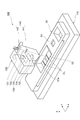
- FIG. 1 is a perspective view of an optical head of a fluorescence measuring apparatus and a chromatographic test tool.
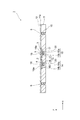
- FIG. 2 is a plan view of a reference body according to an embodiment of the present disclosure.
- FIG. 3 is a cross-sectional view of the reference body taken along line III-III in FIG.
- FIG. 4 is a plan view of the main body of the reference body of FIG.
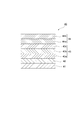
- FIG. 5 is a cross-sectional view of a semiconductor phosphor that constitutes the reference phosphor of FIG.
- FIG. 6A is a perspective view of a first modification of the reference phosphor according to an embodiment of the present disclosure.
- FIG. 6B is a perspective view of a second modification of the reference phosphor according to an embodiment of the present disclosure.
- FIG. 1 is a perspective view of an optical head of a fluorescence measuring apparatus and a chromatographic test tool.
- FIG. 2 is a plan view of a reference body according to an embodiment of the present disclosure.
- FIG. 3 is
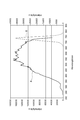
- FIG. 7 is a diagram illustrating a fluorescence excitation spectrum of a phosphor according to an embodiment of the present disclosure.
- FIG. 8 is a diagram illustrating a fluorescence profile obtained by fluorescence measurement of a reference body according to an embodiment of the present disclosure.
- a fluorescence measurement device 100 shown in FIG. 1 is a fluorescence measurement device (fluorescence immunochromatography reader) used for an immunochromatography assay.
- the fluorescence measurement apparatus 100 includes a support base 110, an optical head 120, and a scanning mechanism (not shown).
- the support stand 110 supports the chromatographic test tool 50.
- the chromatographic test tool 50 includes a casing 51 and a chromatographic test piece 52.
- the casing 51 has a rectangular plate shape in which the X-axis direction is the longitudinal direction and the Z-axis direction is the thickness direction.
- the casing 51 has an opening 51a that opens on one side in the Z-axis direction.
- the chromatographic test piece 52 is accommodated in the casing 51.
- a plurality of color lines CL extending along the Y-axis direction are formed in the casing 51.
- the plurality of color lines CL are arranged along the X-axis direction and are exposed to the outside through the opening 51a. Since each color line CL includes a fluorescent substance (and a fluorescent reagent containing them) bound to an antigen or an antibody, each color line CL is fluorescent in the second wavelength region by excitation light in the first wavelength region. To emit.
- the optical head 120 includes an irradiation optical system 130 that irradiates the chromatographic test tool 50 with excitation light in the first wavelength range, a detection optical system 140 that detects fluorescence in the second wavelength range emitted from the chromatographic test tool 50, and have.
- the irradiation optical system 130 includes a semiconductor light emitting element 131, a collimator lens 132, a light beam shaping member 133, a short pass filter 134, and a condenser lens 135.
- the detection optical system 140 includes a long pass filter 141 and a semiconductor light receiving element 142.
- the fluorescence measuring apparatus 100 has a mechanism that does not allow disturbance light to enter.
- the optical head 120 is scanned in the X-axis direction by the scanning mechanism.
- the excitation light in the first wavelength range emitted from the semiconductor light emitting element 131 is irradiated to the chromatographic test tool 50 through the collimator lens 132, the light beam shaping member 133, the short pass filter 134, and the condenser lens 135. Is done.
- fluorescence in the second wavelength region is emitted from each color line CL, and the fluorescence is emitted from the semiconductor light receiving element 142 via the long pass filter 141. Is incident on. Thereby, the coloration degree of each color line CL is measured.
- the first wavelength range refers to light (excitation light) having energy necessary to excite electrons in a fluorescent material that emits fluorescence in the second wavelength range to emit fluorescence in the second wavelength range. It is a wavelength range. Therefore, normally, the first wavelength range and the second wavelength range do not overlap in the wavelength range, and the peak wavelength of the first wavelength range is shorter than the peak wavelength of the second wavelength range.
- the first wavelength range that is the wavelength range of the excitation light is determined according to the excitation characteristics of the fluorescent substance used
- the second wavelength range that is the wavelength range of the fluorescence emitted by the color line CL is the color line CL.
- the first wavelength range is adjusted by the type of the semiconductor light emitting element 131 and the short pass filter 134 and the like.
- the reference body 1 shown in FIGS. 2 and 3 is used for calibration of the fluorescence measuring apparatus 100 described above.
- the reference body 1 has a rectangular plate shape in which the X-axis direction is a longitudinal direction and the Z-axis direction is a thickness direction.
- the shape and size of the reference body 1 are shapes and sizes according to the chromatographic test tool 50.
- the reference body 1 includes a support 10, a first phosphor 20, and a second phosphor 30.
- the reference body 1 further includes a first light transmission member 2, a second light transmission member 3, a first optical coupling material 4, and a second optical coupling material 5.
- the support 10 has a main body 11 and a lid 12.
- Each of the main body 11 and the lid 12 has a rectangular plate shape in which the X-axis direction is the longitudinal direction and the Z-axis direction is the thickness direction.
- the lid 12 is disposed on the surface 11 a (the surface on one side in the Z-axis direction) of the main body 11, and is fixed to the main body 11 by the bolt 6.
- the surface 11a of the main body 11 is provided with a first accommodation space 14 and a second accommodation space 15 that open to one side in the Z-axis direction.
- the first accommodation space 14 and the second accommodation space 15 are arranged along the X-axis direction.
- the first accommodating space 14 includes a first recess 14a formed on the surface 11a of the main body 11 and a first widened portion 14b widened on the opening side of the first recess 14a.
- the second housing space 15 includes a second recess 15a formed on the surface 11a of the main body 11 and a second widened portion 15b widened on the opening side of the second recess 15a.
- the first phosphor 20 is disposed in the first recess 14a.
- the first phosphor 20 is held by a first wall portion (first holding portion) 16 that defines a first recess 14a.
- the first phosphor 20 emits the first fluorescence in the second wavelength region when irradiated with the first excitation light in the first wavelength region.
- the first light transmission member 2 is disposed in the first widened portion 14b.
- the first light transmission member 2 transmits the first excitation light irradiated on the first phosphor 20 and the first fluorescence emitted from the first phosphor 20.
- the first light transmission member 2 has a function of changing the characteristics of the first excitation light.
- the first light transmission member 2 has a light reduction function for reducing the amount of transmitted first excitation light, a wavelength selection function for transmitting only light having a specific wavelength range, and the like.
- a first optical coupling material 4 is disposed between the first phosphor 20 and the first light transmission member 2.
- the first optical coupling material 4 optically couples the first phosphor 20 and the first light transmission member 2, and optically transmits light between the first phosphor 20 and the first light transmission member 2. Changes in the physical properties (wavelength, light quantity, etc.) are suppressed.
- the first optical binder 4 may be a resin having optical transparency and adhesiveness. In FIG. 4, the first light transmission member 2 and the first optical coupling material 4 are indicated by a two-dot chain line.
- the second phosphor 30 is disposed in the second recess 15a.
- the 2nd fluorescent substance 30 is hold
- the second phosphor 30 emits the second fluorescence in the second wavelength region when irradiated with the second excitation light in the first wavelength region.
- the second light transmission member 3 is disposed in the second widened portion 15b.
- the second light transmission member 3 transmits the second excitation light emitted to the second phosphor 30 and the second fluorescence emitted from the second phosphor 30.
- the second light transmission member 3 has a function of changing the characteristics of the second excitation light.
- the second light transmission member 3 has a dimming function for reducing the amount of the second excitation light to be transmitted, a wavelength selection function for transmitting only light having a specific wavelength range, and the like.
- the second optical coupling material 5 is disposed between the second phosphor 30 and the second light transmitting member 3, the second optical coupling material 5 is disposed.
- the second optical coupling material 5 optically couples the second phosphor 30 and the second light transmission member 3 and optically transmits light between the second phosphor 30 and the second light transmission member 3. Changes in the physical properties (wavelength, light quantity, etc.) are suppressed.
- the second optical binder 5 may be a resin having optical transparency and adhesiveness. In FIG. 4, the second light transmission member 3 and the second optical coupling material 5 are indicated by a two-dot chain line.
- the main body 11 is made of a light-shielding material (light-absorbing or light-reflecting), and more preferably made of a light-absorbing material (for example, black ABS resin). That is, the first wall portion 16 and the second wall portion 17 have light shielding properties. Therefore, the first wall portion 16 and the second wall portion 17 also function as the light shielding portion 13 that shields light incident between the first accommodation space 14 and the second accommodation space 15.
- a light-shielding material light-absorbing or light-reflecting
- a light-absorbing material for example, black ABS resin
- the lid portion 12 is provided with a first light passage portion 18 and a second light passage portion 19.
- Each of the first light passage portion 18 and the second light passage portion 19 is a slit extending along the Y-axis direction, and has the same size and shape.
- the first light passage part 18 faces the first accommodation space 14 in the Z-axis direction
- the second light passage part 19 faces the second accommodation space 15 in the Z-axis direction.
- the first light transmission member 2 is disposed between the first light passage portion 18 and the first phosphor 20
- the second light transmission member 3 is composed of the second light passage portion 19 and the second phosphor. 30. Note that the shapes and sizes of the first light passage 18 and the second light passage 19 may be appropriately adjusted according to the shape and size of the color line CL of the chromatographic test tool 50.
- the lid 12 is made of a light-shielding material, more preferably a light-absorbing material (for example, a black acrylic resin).
- a light-absorbing material for example, a black acrylic resin.
- the first region 18a surrounding the first light passage portion 18 and the second region 19a surrounding the second light passage portion 19 in the lid portion 12 have light shielding properties (for example, light absorption properties).
- the first phosphor 20 is a phosphor that emits first fluorescence in the second wavelength region when irradiated with the first excitation light in the first wavelength region
- the second phosphor 30 is the first phosphor in the first wavelength region. It is a phosphor that emits second fluorescence in the second wavelength region when irradiated with double excitation light.
- the first phosphor 20 and the second phosphor 30 are composed of the semiconductor phosphor 40 shown in FIG. 5, and include a substrate 41, a graded layer 42 disposed on the substrate 41, A semiconductor layer 43 disposed on the graded layer 42 and an antioxidant layer 44 disposed on the semiconductor layer 43 are provided.
- the thickness of each layer is made uniform regardless of the actual thickness.
- the first phosphor 20 and the second phosphor 30 are housed in the first housing space 14 and the second housing space 15 so that the oxidation layer 44 side of the semiconductor layer 43 is the lid portion 12 side.
- the semiconductor layer 43 includes a barrier layer 43a, a light emitting layer 43b, and a window layer 43c.
- the barrier layer 43a is disposed on the substrate 41 side with respect to the light emitting layer 43b
- the window layer 43c is disposed on the lid 12 side with respect to the light emitting layer 43b.
- the light emitting layer 43b is a fluorescent material that emits fluorescence (first fluorescence or second fluorescence) in the second wavelength region when irradiated with excitation light (first excitation light or second excitation light) in the first wavelength region. It is made of semiconductor material.
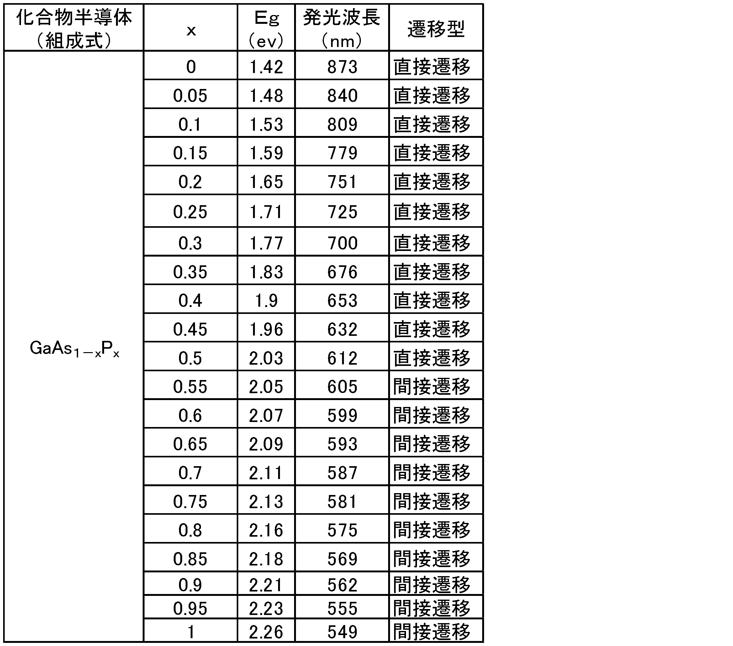
- the semiconductor material constituting the light emitting layer 43b is a compound semiconductor containing Ga, for example, a mixed crystal of GaAs and GaP, which is represented by GaAs (1-x) P x (0 ⁇ x ⁇ 1) ( Hereinafter, it is also simply referred to as “GaAsP”).
- x is preferably 0.5 or less from the viewpoint that the transition type becomes a direct transition type and is excellent in luminous efficiency.
- Such a phosphor is particularly preferable as a phosphor in the red region.
- the emission wavelength (fluorescence wavelength) shown in Table 1 is a value calculated from the band gap energy Eg.
- the thickness of the light emitting layer 43b is 0.01 to 5 ⁇ m.
- the light emitting layer 43b in the first phosphor 20 and the light emitting layer 43b in the second phosphor 30 have different thicknesses. Since the amount of fluorescence (first fluorescence and second fluorescence) emitted by the semiconductor phosphor 40 increases in proportion to the thickness of the light emitting layer 43b, in the present embodiment, the first light incident on the first light passage portion 18 is used. When the amount of excitation light and the amount of second excitation light incident on the second light passage portion 19 are equal to each other, the amount of first fluorescence emitted from the first light passage portion 18 and the second light passage portion 19 are emitted from the second light passage portion 19.
- the amount of the second fluorescent light is different from each other.
- the thickness of the light emitting layer 43b becomes a certain value or more, the amount of fluorescent light hardly increases. Therefore, it is preferable that at least one of the first phosphor 20 and the second phosphor 30 has a light emitting layer 43b having a thickness of 3 ⁇ m or less.
- the barrier layer 43a and the window layer 43c are formed of a semiconductor material represented by Al y Ga (1-y) As (1-z) Pz (0 ⁇ y ⁇ 1, 0 ⁇ z ⁇ 1) (hereinafter simply “AlGaAsP”). It is also a layer composed of. As an example, the barrier layer 43a has a thickness of 0.01 to 5 ⁇ m, and the window layer 43c has a thickness of 0.01 to 5 ⁇ m.
- the antioxidant layer 44 has a function of preventing the semiconductor layer 43 from being oxidized.
- the antioxidant layer 44 includes, for example, an antireflection layer 44a and a protective layer 44b disposed on the opposite side of the semiconductor layer 43 with respect to the antireflection layer 44a.
- the antireflection layer 44a is a layer having a function of preventing reflection of excitation light incident on the light emitting layer 43b in addition to an antioxidation function.
- the protective layer 44b is a layer that protects the surface exposed to the lid 12 side of the semiconductor phosphor 40 from physical and chemical factors.
- the antireflection layer 44a has a layer containing Si 3 N 4 and the protective layer 44b has a layer containing SiO 2 .
- the thickness of the antireflection layer 44a is 0.01 to 0.3 ⁇ m
- the thickness of the protective layer 44b is 0.01 to 0.5 ⁇ m.
- the substrate 41 has a function of fixing the semiconductor layer 43.
- it is a GaAs substrate.
- the thickness of the substrate 41 is 100 to 1200 ⁇ m.
- the graded layer 42 is a layer having a function of relaxing lattice mismatch between the substrate 41 and the semiconductor layer 43.
- the graded layer 42 is a layer containing Ga, As, and P (for example, a layer made of GaAsP) like the semiconductor layer 43.
- the graded layer 42 increases as P approaches the semiconductor layer 43 side from the substrate 41 side. It is comprised so that content may increase.
- the graded layer 42 is configured such that the P content is approximately the same as that of the semiconductor layer 43 in the vicinity of the interface with the semiconductor layer 43.
- the graded layer 42 may be a layer further containing Al (for example, a layer made of AlGaAsP).
- graded layer 42 When graded layer 42 further contains Al, graded layer 42 may be constituted so that content of Al may increase as it approaches the semiconductor layer 43 side from substrate 41 side, and the content is the semiconductor layer. In the vicinity of the interface with the semiconductor layer 43, the semiconductor layer 43 may have the same degree.
- a graded layer 42, a barrier layer 43a, a light emitting layer 43b, and a window layer 43c are grown in this order on a substrate 41, and an antireflection layer 44a and a protective layer 44b are formed thereon. It is obtained by forming the film in this order.
- the calibration of the fluorescence measuring apparatus 100 means an operation for confirming whether or not there is a deviation from a reference value such as a fluorescence intensity or a profile measured by the fluorescence measuring apparatus 100.
- the reference body 1 according to the present embodiment is useful for, for example, shipping adjustment and periodic inspection of the fluorescence measuring apparatus 100. For example, when the fluorescence measuring apparatus 100 is shipped, first, fluorescence measurement of the reference body 1 according to the present embodiment is performed with a reference machine.
- the fluorescence measurement apparatus 100 (actual machine) to be inspected performs fluorescence measurement of the reference body 1 according to the present embodiment, and the emission intensity and profile measured by the reference machine, and the emission intensity and profile measured by the actual machine. Check for deviation from the above. At this time, if the light emission intensity, profile, etc. of the actual machine are not within the specified values, the machine base is adjusted. Through such calibration work, the fluorescence measuring apparatus 100 capable of performing stable fluorescence measurement can be shipped. Moreover, at the time of periodic inspection of the fluorescence measuring apparatus 100, the fluorescence intensity of the reference body 1 according to this embodiment is measured, and the measured emission intensity, profile, etc. are compared with the emission intensity, profile, etc. measured by the reference machine.
- the measurement sensitivity can be confirmed in a wide dynamic range by a single measurement.
- the support body 10 is each provided with the main-body part 11 and the cover part 12, the main-body part 11 and the cover part 12 can be comprised with the material according to each function.
- the cover part 12 is being fixed to the main-body part 11 with the volt
- the first housing space 14 and the second housing space 15 have regions where the first phosphor 20 and the second phosphor 30 are not housed, the first phosphor 20 and the second phosphor 30 are not disposed. Removal can be performed easily.
- the main body portion 11 includes the first holding portion and the second holding portion, the first phosphor 20 is held in the first accommodation space 14 and the second fluorescence is obtained in the second accommodation space 15.
- the body 30 is held.
- the main body 11 is made of a light-shielding material, light incident between the first accommodation space 14 and the second accommodation space 15 can be shielded. Incidence of excitation light and emission of fluorescence from regions other than the light passage portion 18 and the second light passage portion 19 can be suppressed. Therefore, it is possible to suppress the excitation light and fluorescence in one phosphor from affecting the excitation light and fluorescence in the other phosphor.
- the main body 11 is made of a material having a light absorption property, it is possible to suppress the influence of excitation light and fluorescence scattering in fluorescence measurement.
- the first wall portion 16 and the second wall portion 17 have light shielding properties, the first wall portion 16 and the second wall portion 17 are connected to the first accommodation space 14 and the second accommodation space 15. It also functions as a light-shielding portion 13 that shields light incident between them. Therefore, the fluorescent substance accommodated in one accommodation space is hard to receive the influence of the light (excitation light and fluorescence) leaked from the wall part of the other accommodation space. Thereby, since the dispersion
- the lid 12 is made of a light-shielding material, and the first region 18 a surrounding the first light passage 18 and the second region 19 a surrounding the second light passage 19 are light-shielding. Therefore, it is possible to suppress the influence of the light irradiated on the first region 18a (first excitation light) and the light irradiated on the second region 19a (second excitation light) on the fluorescence measurement. Thereby, since the dispersion
- the first region 18a and the second region 19a are made of a light-absorbing material, variations in measurement values due to noise components such as scattered light are suppressed.
- the first light transmitting member 2 that is disposed between the first light passing portion 18 and the first phosphor 20 and transmits the first excitation light and the first fluorescence, and the second light passing portion. 19 and the second phosphor 30, and the second light transmitting member 3 that transmits the second excitation light and the second fluorescence, the first phosphor 20 due to physical and chemical factors. And degradation of the 2nd fluorescent substance 30 can be prevented. Thereby, calibration can be performed with high accuracy over a long period of time.
- the first optical coupling material 4 and the first light transmission member 2 and the second phosphor 30 and the second light transmission member 3 are respectively connected between the first phosphor 20 and the first light transmission member 2. 2 Since it is filled with the optical binder 5, the optical loss at the interface between the phosphor and the light transmitting member is suppressed. Thereby, since the dispersion
- the phosphors (the first phosphor 20 and the second phosphor 30) are composed of the semiconductor phosphor 40, and the semiconductor material constituting the light emitting layer 43b of the semiconductor phosphor 40 contains Ga. Since it is a compound semiconductor, as will be described later, the fluorescence characteristics can be easily changed by adjusting the type of compound material and its content. In the present embodiment, since the semiconductor material constituting the light emitting layer 43b is a compound semiconductor represented by GaAs (1-x) P x (0 ⁇ x ⁇ 1), good fluorescence is obtained particularly in the red region. It is done.
- the barrier layer 43a made of AlGaAsP, the light emitting layer 43b made of GaAsP, and the window layer 43c made of AlGaAsP are laminated in this order, and the semiconductor layer 43 is a so-called well. Since it has a mold structure, it has excellent luminous efficiency. In the present embodiment, since the semiconductor phosphor 40 includes the oxidation preventing layer 44, the phosphor can be prevented from being deteriorated due to oxidation, and calibration can be performed with high accuracy over a long period of time.
- the semiconductor phosphor 40 described above has a fluorescence excitation spectrum close to the fluorescence excitation spectrum of a reagent for red excitation generally used in an immunochromatography assay
- the fluorescence measuring apparatus 100 used in an immunochromatography assay ( It can be suitably used as a calibration standard for an immunochromatography reader.
- this indication is not limited to the above-mentioned embodiment.
- the reference body may not include the bolt 6, and for example, the main body portion 11 and the lid portion 12 may be fixed by an adhesive resin.
- the main-body part 11 and the cover part 12 may be shape
- first wall portion 16 and the second wall portion 17 and portions other than the first wall portion 16 and the second wall portion 17 may be made of different materials.
- first wall part 16 and the second wall part 17 may be made of a light-shielding material.
- only one of the first wall portion 16 and the second wall portion 17 may be made of a light-shielding material.
- the first wall portion 16 and the second wall portion 17 do not have a light shielding property, and a light shielding member may be separately provided between the first accommodation space 14 and the second accommodation space 15.
- the first region 18a and the second region 19a and portions other than the first region 18a and the second region 19a may be made of different materials.
- the cover part 12 only the 1st area
- only one of the first region 18a and the second region 19a may be made of a light-shielding material.
- the first region 18a and the second region 19a are not light-shielding, and a light-shielding member may be separately provided between the first region 18a and the second region 19a.
- first light passage 18 and the second light passage 19 may be made of a light transmissive material.
- the first light passage portion 18 and the second light passage portion 19 may be light transmissive regions formed in the lid portion 12.
- the fluorescent property of the phosphor may be changed by changing the P content ratio x in GaAs (1-x) P x constituting the light emitting layer 43b.
- Increasing the content ratio x (making x closer to 1) increases the band gap energy, so that the fluorescence wavelength region (second wavelength region) can be shifted to the short wavelength side. Since the direct transition occurs when the content ratio x is 0.5 or less, the fluorescence intensity tends to be excellent.
- the fluorescent property of the phosphor may be changed by changing the content ratio z.
- the content ratio y in the window layer 43c may be 0.05 to 1.
- the content ratio y in the barrier layer 43a may be 0.05 to 1.
- the light emitting layer 43b may include a material other than a semiconductor material.
- the semiconductor material contained in the light emitting layer 43b is not limited to GaAsP.
- the semiconductor material contained in the light emitting layer 43b is, for example, InGaAs, InGaP, InAsP, AlInAs, AlAsP, AlGaAs, AlGaP, InGaN, AlGaN, InNAs, GaNAs, InGaAsP, AlInGaAs, AlInGaP, AlInAsP, AlGaAsP, GaInNAs, AlInGaN, AlInNAs. AlGaNAs, AlInGaAsP, AlGaInNAs, etc.
- the fluorescence characteristics of the phosphor can be changed. That is, the wavelength range (second wavelength range) of the fluorescence emitted from the phosphor can be changed by changing the semiconductor material.
- Table 2 shows fluorescence wavelengths (emission wavelengths) assumed when each compound semiconductor is used as a phosphor.
- the emission wavelength shown in Table 2 is a value calculated from the band gap energy Eg.
- the window layer 43c and the barrier layer 43a may include a material other than a semiconductor material.
- the semiconductor material contained in the window layer 43c and the barrier layer 43a is not limited to AlGaAsP.
- the semiconductor materials contained in the window layer 43c and the barrier layer 43a are, for example, AlGaAs, AlGaP, AlGaN, InNAs, GaNAs, InGaAsP, AlInGaAs, AlInGaP, AlInAsP, GaInNAs, AlInAs, AlAsP, AlInGaN, AlGaAsP, AlInNAs, AlGaNAs, and AlInGaAsP. AlGaInNAs or the like may be used.
- the semiconductor layer 43 may not include the window layer 43c and the barrier layer 43a.
- the antioxidant layer 44 may be composed of only one of the antireflection layer 44a or the protective layer 44b, and may have other layers other than the antireflection layer 44a and the protective layer 44b. You may consist only of layers other than the layer 44a and the protective layer 44b.
- Antireflective layer 44a may contain components other than Si 3 N 4, it may be constituted by components other than Si 3 N 4.
- Protective layer 44b may contain components other than SiO 2, it may be constituted by components other than SiO 2.
- the phosphor may not include the antioxidant layer 44.
- the phosphor may be composed of the fluorescent resin 60.
- the fluorescent resin 60 contains a light-transmitting resin and a fluorescent substance (and a fluorescent reagent containing the fluorescent substance) dispersed in the light-transmitting resin.
- the fluorescent reagent may be liquid or solid.
- Examples of the fluorescent reagent include organic dyes such as Alexa Fluor 647 (manufactured by Thermo Fisher Scientific Co., Ltd., “Fluor” is a registered trademark), semiconductor crystals such as Q-dot, metal complexes such as DTBTA-Eu 3+, and the like. Can be used.
- the fluorescent resin 60 is used as the phosphor, for example, the amount of fluorescent light can be adjusted by adjusting the concentration of the fluorescent substance in the fluorescent resin 60.
- the fluorescent resin 60 is used by being fixed in a fixing member 61, for example, as shown in FIG. That is, the reference member is produced by accommodating the fixing member 61 in the first accommodation space 14 and the second accommodation space 15.
- the fixing member 61 shown in FIG. 6A is made by mixing carbon, boron, or the like into a light-transmitting substrate 63 such as glass and a resin having a light shielding property (for example, PDMS (polydimethylsiloxane)).
- a flow path 62 made of The fluorescent resin 60 can be manufactured, for example, by the following method. First, a light transmissive ultraviolet curable resin and a fluorescent reagent are mixed to prepare a resin composition.
- the resin composition is injected into the flow path 62 of the fixing member 61 shown in FIG. 6A using a pipette.
- the resin composition is cured by irradiating ultraviolet rays from the light transmissive substrate 63 side of the fixing member 61.
- the fluorescent resin 60 fixed in the fixing member 61 can be obtained.
- the phosphor may be composed of a fluorescent glass 70 shown in FIG.
- the fluorescent glass 70 contains glass and a fluorescent substance (and a fluorescent reagent containing the fluorescent substance) dispersed in the glass.
- the fluorescent glass 70 is used, measurement sensitivity in a desired fluorescence wavelength region can be confirmed by appropriately selecting a fluorescent material.
- fluorescent glass is not easily oxidized, calibration can be performed with high accuracy over a long period of time.
- An example of the fluorescent reagent is the same as the example of the fluorescent reagent used for the fluorescent resin 60.
- the fluorescent glass 70 for example, commercially available products such as “Lumilas-R7”, “Lumilas-G9”, and “Lumilas-B” manufactured by Sumita Optical Glass Co., Ltd. can be used.
- the fluorescent resin 60 described above may be a phosphor having a shape as shown in FIG.
- the same phosphor may be used as the first phosphor 20 and the second phosphor 30.
- the amount of second fluorescence emitted from the passage unit 19 is adjusted.
- the adjustment of the amount of light may be performed by a method of changing the shape and size of the first light passage unit 18 and the second light passage unit 19, for example.
- the shape of the 1st light passage part 18 and the 2nd light passage part 19 may be a slit which has a mesh structure.
- the light amount can be reduced by forming the regions with materials having different light transmissive properties. Adjustments may be made. Further, the amount of light may be adjusted by using the first light transmitting member 2 and the second light transmitting member 3 made of materials having different light transmittances. Examples of such a member include an ND filter (a neutral density filter). Moreover, you may combine the light quantity adjustment means mentioned above.
- Example 1 A GaAs substrate (thickness: 350 ⁇ m) is prepared, and a graded layer (thickness: 10 ⁇ m), a barrier layer (thickness: 0.1 ⁇ m), a light emitting layer (thickness: 0.7 ⁇ m), a window layer on the substrate (Thickness: 0.035 ⁇ m) was grown in order.
- the graded layer is a layer containing Ga, As, Al, and P, and the content of Al and P is increased from the substrate side toward the barrier layer side, and the configuration is the same as that of the barrier layer in the vicinity of the interface with the barrier layer. It adjusted so that it might become.
- an antireflection layer (thickness: 0.095 ⁇ m) and a protective layer (thickness: 0.3 ⁇ m) were sequentially formed as an antioxidant layer on the window layer.
- the antireflection layer was made of Si 3 N 4 and the protective layer was made of SiO 2 .
- the semiconductor phosphor was obtained by the above operation.
- the reference phosphor shown in FIGS. 2 to 4 was manufactured using the semiconductor phosphor obtained in Example 1 as the first phosphor and the second phosphor.
- the main body portion of the reference body was made of black ABS resin so that the first wall portion and the second wall portion had light shielding properties.
- the acrylic board comprised with the black acrylic resin was used for the cover part.
- an ND filter (light attenuation rate: 80%) was used as the first light transmission member, and an ND filter (light attenuation rate: 90%) was used as the second light transmission member.
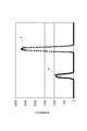
- FIG. 7 is a diagram showing a fluorescence excitation spectrum of the semiconductor phosphor itself.
- the spectrum A shows the spectrum of the excitation light irradiated on the semiconductor phosphor
- the spectrum B shows the spectrum of the fluorescence emitted from the semiconductor phosphor by the irradiation of the excitation light.
- the horizontal axis indicates the wavelength
- the vertical axis indicates the intensity.
- the left vertical axis indicates the intensity of the excitation spectrum
- the right vertical axis indicates the intensity of the fluorescence spectrum.
- the semiconductor phosphor of Example 1 emitted fluorescence having a peak at 730 nm by excitation light having a wavelength region of 450 nm to 700 nm.
- FIG. 8 is a diagram showing a fluorescence profile obtained by fluorescence measurement of a reference body using the fluorescence immunochromatography reader shown in FIG.
- the vertical axis represents the intensity of the first fluorescence (a in FIG. 8) and the second fluorescence (b in FIG. 8).
- measurement sensitivity can be confirmed stably and in a wide dynamic range by one measurement.
- SYMBOLS 1 DESCRIPTION OF SYMBOLS 1 ... Reference
Landscapes
- Health & Medical Sciences (AREA)
- Physics & Mathematics (AREA)
- General Physics & Mathematics (AREA)
- Immunology (AREA)
- Chemical & Material Sciences (AREA)
- Analytical Chemistry (AREA)
- Biochemistry (AREA)
- General Health & Medical Sciences (AREA)
- Pathology (AREA)
- Life Sciences & Earth Sciences (AREA)
- Nuclear Medicine, Radiotherapy & Molecular Imaging (AREA)
- Engineering & Computer Science (AREA)
- Mathematical Physics (AREA)
- Theoretical Computer Science (AREA)
- Spectroscopy & Molecular Physics (AREA)
- Investigating, Analyzing Materials By Fluorescence Or Luminescence (AREA)
- Investigating Or Analysing Materials By The Use Of Chemical Reactions (AREA)
Abstract
Description

GaAs基板(厚さ:350μm)を用意し、当該基板上にグレーデッド層(厚さ:10μm)、障壁層(厚さ:0.1μm)、発光層(厚さ:0.7μm)、窓層(厚さ:0.035μm)を順に成長させた。グレーデッド層は、Ga、As、Al及びPを含む層とし、基板側から障壁層側に近づくに従ってAl及びPの含有量を増加させ、障壁層との界面付近において障壁層と同様の構成となるように調整した。また、障壁層はAlyGa(1-y)As(1-z)Pz(y=0.65、z=0.23)で構成し、発光層はGaAs(1-x)Px(x=0.23)で構成し、窓層はAlyGa(1-y)As(1-z)Pz(y=0.65、z=0.23)で構成した。次いで、窓層上に、酸化防止層として反射防止層(厚さ:0.095μm)及び保護層(厚さ:0.3μm)を順に成膜した。反射防止層は、Si3N4で構成し、保護層はSiO2で構成した。以上の操作により半導体蛍光体を得た。
図1に示される蛍光イムノクロマトリーダーを用いて、得られた基準体の蛍光測定を行った。励起においては、半導体発光素子に655nm半導体レーザーを用い、ショートパスフィルタに670nmショートパスフィルタを用いた。また、蛍光測定には、ロングパスフィルタに690nmロングパスフィルタを用い、半導体受光素子にSi-フォトダイオードを用いた。励起光の照射は1mWで行った。結果を図7及び図8に示す。
Claims (15)
- 第1光通過部及び第2光通過部、並びに、前記第1光通過部と対向する第1収容空間及び前記第2光通過部と対向する第2収容空間が設けられた支持体と、
前記第1収容空間に収容され、第1波長域の第1励起光が前記第1光通過部を介して照射されたときに第2波長域の第1蛍光を発する第1蛍光体と、
前記第2収容空間に収容され、前記第1波長域の第2励起光が前記第2光通過部を介して照射されたときに前記第2波長域の第2蛍光を発する第2蛍光体と、
前記第1収容空間と前記第2収容空間との間に配置された遮光部と、を備え、
前記第1光通過部に入射する前記第1励起光の光量と前記第2光通過部に入射する前記第2励起光の光量とが互いに等しい場合に、前記第1光通過部から出射する前記第1蛍光の光量と前記第2光通過部から出射する前記第2蛍光の光量とは互いに異なる、蛍光測定装置の校正用基準体。 - 前記支持体は、
前記第1収容空間に収容された前記第1蛍光体を保持する第1保持部と、
前記第2収容空間に収容された前記第2蛍光体を保持する第2保持部と、を有する、請求項1に記載の基準体。 - 前記第1保持部は、前記第1収容空間を画定する第1壁部であり、
前記第2保持部は、前記第2収容空間を画定する第2壁部であり、
前記第1壁部及び前記第2壁部の少なくとも一方は、前記遮光部を構成する、請求項2に記載の基準体。 - 前記支持体のうち、少なくとも、前記第1光通過部を囲む第1領域及び前記第2光通過部を囲む第2領域は遮光性を有する、請求項1~3のいずれか一項に記載の基準体。
- 前記支持体は、
前記第1収容空間及び前記第2収容空間が設けられた本体部と、
前記第1光通過部及び前記第2光通過部が設けられた蓋部と、有する、請求項1~4のいずれか一項に記載の基準体。 - 前記第1光通過部と前記第1蛍光体との間に配置され、前記第1励起光及び前記第1蛍光を透過させる第1光透過部材と、
前記第2光通過部と前記第2蛍光体との間に配置され、前記第2励起光及び前記第2蛍光を透過させる第2光透過部材と、を更に備える、請求項1~5のいずれか一項に記載の基準体。 - 前記第1蛍光体と前記第1光透過部材との間に配置された第1光学的結合材と、
前記第2蛍光体と前記第2光透過部材との間に配置された第2光学的結合材と、を更に備える、請求項6に記載の基準体。 - 前記第1光透過部材は、前記第1励起光の特性を変化させる機能を有し、
前記第2光透過部材は、前記第2励起光の特性を変化させる機能を有する、請求項6又は7に記載の基準体。 - 前記第1蛍光体及び前記第2蛍光体のうちの少なくとも一方は、蛍光物質として半導体材料を含有する発光層を有する半導体層を備える、請求項1~8のいずれか一項に記載の基準体。
- 前記半導体材料は、Gaを含む化合物半導体である、請求項9に記載の基準体。
- 前記化合物半導体はGaAs(1-x)Px(0≦x≦1)である、請求項10に記載の基準体。
- 前記半導体層は、前記発光層の前記励起光が入射する側及びその反対側にAlGaAsPを含む層を更に有する、請求項9~11のいずれか一項に記載の基準体。
- 前記第1蛍光体及び前記第2蛍光体のうちの少なくとも一方は、前記発光層の前記励起光が入射する側に酸化防止層を更に備える、請求項9~12のいずれか一項に記載の基準体。
- 前記第1蛍光体及び前記第2蛍光体のうちの少なくとも一方は、光透過性樹脂と、前記光透過性樹脂中に分散された蛍光物質とを含有する蛍光樹脂で構成されている、請求項1~8のいずれか一項に記載の基準体。
- 前記第1蛍光体及び前記第2蛍光体のうちの少なくとも一方は、ガラスと、前記ガラス中に分散された蛍光物質とを含有する蛍光ガラスで構成されている、請求項1~8のいずれか一項に記載の基準体。
Priority Applications (5)
| Application Number | Priority Date | Filing Date | Title |
|---|---|---|---|
| US16/098,891 US20190187058A1 (en) | 2016-05-19 | 2017-02-23 | Calibration reference body for fluorescence measurement device |
| EP17798948.0A EP3460457A4 (en) | 2016-05-19 | 2017-02-23 | CALIBRATION REFERENCE BODY FOR FLUORESCENCE MEASURING DEVICE |
| JP2018518095A JP6646742B2 (ja) | 2016-05-19 | 2017-02-23 | 蛍光測定装置の校正用基準体 |
| CN201780030146.2A CN109154570A (zh) | 2016-05-19 | 2017-02-23 | 荧光测定装置的校正用基准体 |
| KR1020187025439A KR20190010529A (ko) | 2016-05-19 | 2017-02-23 | 형광 측정 장치의 교정용 기준체 |
Applications Claiming Priority (2)
| Application Number | Priority Date | Filing Date | Title |
|---|---|---|---|
| JP2016100683 | 2016-05-19 | ||
| JP2016-100683 | 2016-05-19 |
Publications (1)
| Publication Number | Publication Date |
|---|---|
| WO2017199510A1 true WO2017199510A1 (ja) | 2017-11-23 |
Family
ID=60325014
Family Applications (1)
| Application Number | Title | Priority Date | Filing Date |
|---|---|---|---|
| PCT/JP2017/006774 Ceased WO2017199510A1 (ja) | 2016-05-19 | 2017-02-23 | 蛍光測定装置の校正用基準体 |
Country Status (7)
| Country | Link |
|---|---|
| US (1) | US20190187058A1 (ja) |
| EP (1) | EP3460457A4 (ja) |
| JP (1) | JP6646742B2 (ja) |
| KR (1) | KR20190010529A (ja) |
| CN (1) | CN109154570A (ja) |
| TW (1) | TW201741654A (ja) |
| WO (1) | WO2017199510A1 (ja) |
Cited By (4)
| Publication number | Priority date | Publication date | Assignee | Title |
|---|---|---|---|---|
| WO2020137532A1 (ja) * | 2018-12-28 | 2020-07-02 | テルモ株式会社 | テストストリップ及び成分測定システム |
| WO2022168374A1 (ja) * | 2021-02-02 | 2022-08-11 | 浜松ホトニクス株式会社 | 照射光学系、照射装置、及び、光学測定装置 |
| EP3889585A4 (en) * | 2018-12-28 | 2022-09-21 | Precision Biosensor Inc. | REFERENCE CASSETTE FOR A FLUORESCENT IMMUNOASSAY DIAGNOSTIC DEVICE |
| JP2025051216A (ja) * | 2023-09-25 | 2025-04-04 | 東芝情報システム株式会社 | 樹脂特性測定装置及び樹脂特性測定方法 |
Families Citing this family (1)
| Publication number | Priority date | Publication date | Assignee | Title |
|---|---|---|---|---|
| WO2021104987A1 (en) | 2019-11-25 | 2021-06-03 | Surgvision Gmbh | Testing of a luminescence imaging apparatus with inclined containers of luminescence substances |
Citations (8)
| Publication number | Priority date | Publication date | Assignee | Title |
|---|---|---|---|---|
| JP2006208386A (ja) | 2005-01-26 | 2006-08-10 | Agilent Technol Inc | 複数の標識を有するアッセイテスト細片及びその読み取り法 |
| US20060208199A1 (en) * | 2005-03-18 | 2006-09-21 | Uvp Inc. | Luminescent calibration |
| WO2006107371A1 (en) * | 2005-03-30 | 2006-10-12 | Kimberly-Clark Worldwide, Inc. | Diagnostic test kits employing an internal calibration system |
| WO2010061772A1 (ja) * | 2008-11-28 | 2010-06-03 | コニカミノルタエムジー株式会社 | イムノクロマト媒体およびイムノクロマトグラフ法 |
| US20110076687A1 (en) * | 2008-04-17 | 2011-03-31 | Qiagen Lake Constance Gmbh | Fluorescence standard, and the use thereof |
| US20110085168A1 (en) * | 2004-06-30 | 2011-04-14 | Life Technologies Corporation | Luminescence Reference Standards |
| US20120179383A1 (en) * | 2011-01-06 | 2012-07-12 | Samsung Electronics Co., Ltd | Disc and calibration method of test device using the same |
| JP2013096920A (ja) * | 2011-11-02 | 2013-05-20 | Hamamatsu Photonics Kk | 蛍光ファントム装置および蛍光イメージング方法 |
Family Cites Families (10)
| Publication number | Priority date | Publication date | Assignee | Title |
|---|---|---|---|---|
| US6242114B1 (en) * | 1994-07-05 | 2001-06-05 | Optical Coating Laboratory | Solid fluorescence reference and method |
| DE202004002064U1 (de) * | 2004-02-11 | 2004-04-15 | Schott Spezialglas Gmbh | Mikroarray-Träger und Biochips mit Fluoreszenzstandards aus Farbglas |
| US20050287040A1 (en) * | 2004-06-29 | 2005-12-29 | Molecular Devices Corporation | Fluorescence validation plate |
| CN1280623C (zh) * | 2004-07-16 | 2006-10-18 | 北京博奥生物芯片有限责任公司 | 一种用于荧光仪器校准测量的校准基片及其制备方法 |
| JP2007064828A (ja) * | 2005-08-31 | 2007-03-15 | Toshiba Corp | 蛍光基準部材、蛍光検査装置、および蛍光基準部材の製造方法 |
| US20070141726A1 (en) * | 2005-12-19 | 2007-06-21 | Agency For Science, Technology And Research | Detection via switchable emission of nanocrystals |
| JP2010101835A (ja) * | 2008-10-27 | 2010-05-06 | Toshiba Corp | 蛍光基準部材、及び蛍光基準部材を備える蛍光検知装置 |
| JP2012093190A (ja) * | 2010-10-26 | 2012-05-17 | Olympus Corp | 蛍光センサの補正方法おび蛍光センサ |
| KR20130078345A (ko) * | 2011-12-30 | 2013-07-10 | 일진엘이디(주) | 스트레인 완충층을 이용하여 발광효율이 우수한 질화물계 발광소자 |
| CN204964393U (zh) * | 2015-09-01 | 2016-01-13 | 中国科学院苏州生物医学工程技术研究所 | 荧光纳米标准板 |
-
2017
- 2017-02-23 WO PCT/JP2017/006774 patent/WO2017199510A1/ja not_active Ceased
- 2017-02-23 EP EP17798948.0A patent/EP3460457A4/en not_active Withdrawn
- 2017-02-23 US US16/098,891 patent/US20190187058A1/en not_active Abandoned
- 2017-02-23 JP JP2018518095A patent/JP6646742B2/ja active Active
- 2017-02-23 KR KR1020187025439A patent/KR20190010529A/ko not_active Withdrawn
- 2017-02-23 CN CN201780030146.2A patent/CN109154570A/zh active Pending
- 2017-03-02 TW TW106106895A patent/TW201741654A/zh unknown
Patent Citations (8)
| Publication number | Priority date | Publication date | Assignee | Title |
|---|---|---|---|---|
| US20110085168A1 (en) * | 2004-06-30 | 2011-04-14 | Life Technologies Corporation | Luminescence Reference Standards |
| JP2006208386A (ja) | 2005-01-26 | 2006-08-10 | Agilent Technol Inc | 複数の標識を有するアッセイテスト細片及びその読み取り法 |
| US20060208199A1 (en) * | 2005-03-18 | 2006-09-21 | Uvp Inc. | Luminescent calibration |
| WO2006107371A1 (en) * | 2005-03-30 | 2006-10-12 | Kimberly-Clark Worldwide, Inc. | Diagnostic test kits employing an internal calibration system |
| US20110076687A1 (en) * | 2008-04-17 | 2011-03-31 | Qiagen Lake Constance Gmbh | Fluorescence standard, and the use thereof |
| WO2010061772A1 (ja) * | 2008-11-28 | 2010-06-03 | コニカミノルタエムジー株式会社 | イムノクロマト媒体およびイムノクロマトグラフ法 |
| US20120179383A1 (en) * | 2011-01-06 | 2012-07-12 | Samsung Electronics Co., Ltd | Disc and calibration method of test device using the same |
| JP2013096920A (ja) * | 2011-11-02 | 2013-05-20 | Hamamatsu Photonics Kk | 蛍光ファントム装置および蛍光イメージング方法 |
Non-Patent Citations (1)
| Title |
|---|
| See also references of EP3460457A4 |
Cited By (9)
| Publication number | Priority date | Publication date | Assignee | Title |
|---|---|---|---|---|
| WO2020137532A1 (ja) * | 2018-12-28 | 2020-07-02 | テルモ株式会社 | テストストリップ及び成分測定システム |
| CN112997067A (zh) * | 2018-12-28 | 2021-06-18 | 泰尔茂株式会社 | 测试条以及成分测定系统 |
| EP3889585A4 (en) * | 2018-12-28 | 2022-09-21 | Precision Biosensor Inc. | REFERENCE CASSETTE FOR A FLUORESCENT IMMUNOASSAY DIAGNOSTIC DEVICE |
| WO2022168374A1 (ja) * | 2021-02-02 | 2022-08-11 | 浜松ホトニクス株式会社 | 照射光学系、照射装置、及び、光学測定装置 |
| JP2022118476A (ja) * | 2021-02-02 | 2022-08-15 | 浜松ホトニクス株式会社 | 照射光学系、照射装置、及び、光学測定装置 |
| JP7704538B2 (ja) | 2021-02-02 | 2025-07-08 | 浜松ホトニクス株式会社 | 照射装置、及び、光学測定装置 |
| US12517037B2 (en) | 2021-02-02 | 2026-01-06 | Hamamatsu Photonics K.K. | Emission optical system, emission device, and optical measurement device |
| JP2025051216A (ja) * | 2023-09-25 | 2025-04-04 | 東芝情報システム株式会社 | 樹脂特性測定装置及び樹脂特性測定方法 |
| JP7688283B2 (ja) | 2023-09-25 | 2025-06-04 | 東芝情報システム株式会社 | 樹脂特性測定装置及び樹脂特性測定方法 |
Also Published As
| Publication number | Publication date |
|---|---|
| JP6646742B2 (ja) | 2020-02-14 |
| EP3460457A4 (en) | 2020-02-26 |
| US20190187058A1 (en) | 2019-06-20 |
| JPWO2017199510A1 (ja) | 2019-03-14 |
| KR20190010529A (ko) | 2019-01-30 |
| EP3460457A1 (en) | 2019-03-27 |
| CN109154570A (zh) | 2019-01-04 |
| TW201741654A (zh) | 2017-12-01 |
Similar Documents
| Publication | Publication Date | Title |
|---|---|---|
| JP6646742B2 (ja) | 蛍光測定装置の校正用基準体 | |
| Karadza et al. | Efficient, high-CRI white LEDs by combining traditional phosphors with cadmium-free InP/ZnSe red quantum dots | |
| CN113892022B (zh) | 光源及生化分析装置 | |
| KR20180031809A (ko) | 분광 측정 장치, 분광 측정 방법 및 시료 용기 | |
| US20180246267A1 (en) | Backlight module, display device to which backlight module is applied, and method for manufacturing light guide plate | |
| JP6399520B2 (ja) | 光測定装置及び光測定方法 | |
| EP3527998A1 (en) | Test apparatus and production method for light-emitting device | |
| Radnik et al. | Composition, thickness, and homogeneity of the coating of core–shell nanoparticles—possibilities, limits, and challenges of X-ray photoelectron spectroscopy | |
| CN109085352A (zh) | 一种免疫层析分析仪用的光学装置 | |
| JP6516484B2 (ja) | 液中溶存物濃度測定装置 | |
| JP2017502280A (ja) | 生物学的物質の画像ベースの表現のためのデバイスのための較正標準 | |
| US20200173920A1 (en) | Optical measuring device, light guide member, and optical measuring method | |
| CN109030427B (zh) | 一种专用光致发光光谱测量的ccd光谱仪 | |
| JP2017120200A5 (ja) | ||
| EP4302014B1 (en) | Methods and apparatus for integrating diamond with led towards on-chip quantum sensing | |
| Karadza et al. | Comparison of different RGB InP-quantum-dot-on-chip LED configurations | |
| US20060147148A1 (en) | Method and apparatus for pixel display and SERS analysis | |
| EP3133386B1 (en) | Sensing module and sensing method | |
| JP5760589B2 (ja) | 白色led装置用蛍光体の蛍光スペクトルの測定方法及び測定装置 | |
| EP4266028A1 (en) | Emission optical system, emission device, and optical measurement device | |
| US20170089835A1 (en) | Sensor Element For Photoluminescence Measurements, Photoluminescence Detection Means, Method For Operating Photoluminescence Detection Means, Method For Producing A Sensor Element And Use Of A Sensor Element | |
| KR20220012947A (ko) | 광전자 소자 및 광전자 소자를 제조하기 위한 방법 | |
| JP7076021B1 (ja) | ライトガイド、電子線検出器、及び荷電粒子装置 | |
| KR102306937B1 (ko) | 바이오 분석기기 검증용 표준물질 조성물 및 이를 이용한 표준 스트립 | |
| KR102257204B1 (ko) | 형광체 필름 및 그의 제조방법과 이를 이용한 광 특성 측정 장치 및 측정 방법 |
Legal Events
| Date | Code | Title | Description |
|---|---|---|---|
| ENP | Entry into the national phase |
Ref document number: 2018518095 Country of ref document: JP Kind code of ref document: A |
|
| ENP | Entry into the national phase |
Ref document number: 20187025439 Country of ref document: KR Kind code of ref document: A |
|
| NENP | Non-entry into the national phase |
Ref country code: DE |
|
| 121 | Ep: the epo has been informed by wipo that ep was designated in this application |
Ref document number: 17798948 Country of ref document: EP Kind code of ref document: A1 |
|
| ENP | Entry into the national phase |
Ref document number: 2017798948 Country of ref document: EP Effective date: 20181219 |