WO2017204013A1 - ホログラフィ観察方法及び装置 - Google Patents
ホログラフィ観察方法及び装置 Download PDFInfo
- Publication number
- WO2017204013A1 WO2017204013A1 PCT/JP2017/018175 JP2017018175W WO2017204013A1 WO 2017204013 A1 WO2017204013 A1 WO 2017204013A1 JP 2017018175 W JP2017018175 W JP 2017018175W WO 2017204013 A1 WO2017204013 A1 WO 2017204013A1
- Authority
- WO
- WIPO (PCT)
- Prior art keywords
- light beam
- semiconductor laser
- observation
- light
- light source
- Prior art date
- Legal status (The legal status is an assumption and is not a legal conclusion. Google has not performed a legal analysis and makes no representation as to the accuracy of the status listed.)
- Ceased
Links
Images


Classifications
-
- G—PHYSICS
- G03—PHOTOGRAPHY; CINEMATOGRAPHY; ANALOGOUS TECHNIQUES USING WAVES OTHER THAN OPTICAL WAVES; ELECTROGRAPHY; HOLOGRAPHY
- G03H—HOLOGRAPHIC PROCESSES OR APPARATUS
- G03H1/00—Holographic processes or apparatus using light, infrared or ultraviolet waves for obtaining holograms or for obtaining an image from them; Details peculiar thereto
- G03H1/04—Processes or apparatus for producing holograms
- G03H1/0465—Particular recording light; Beam shape or geometry
-
- G—PHYSICS
- G03—PHOTOGRAPHY; CINEMATOGRAPHY; ANALOGOUS TECHNIQUES USING WAVES OTHER THAN OPTICAL WAVES; ELECTROGRAPHY; HOLOGRAPHY
- G03H—HOLOGRAPHIC PROCESSES OR APPARATUS
- G03H1/00—Holographic processes or apparatus using light, infrared or ultraviolet waves for obtaining holograms or for obtaining an image from them; Details peculiar thereto
- G03H1/0005—Adaptation of holography to specific applications
-
- G—PHYSICS
- G03—PHOTOGRAPHY; CINEMATOGRAPHY; ANALOGOUS TECHNIQUES USING WAVES OTHER THAN OPTICAL WAVES; ELECTROGRAPHY; HOLOGRAPHY
- G03H—HOLOGRAPHIC PROCESSES OR APPARATUS
- G03H1/00—Holographic processes or apparatus using light, infrared or ultraviolet waves for obtaining holograms or for obtaining an image from them; Details peculiar thereto
- G03H1/02—Details of features involved during the holographic process; Replication of holograms without interference recording
-
- G—PHYSICS
- G03—PHOTOGRAPHY; CINEMATOGRAPHY; ANALOGOUS TECHNIQUES USING WAVES OTHER THAN OPTICAL WAVES; ELECTROGRAPHY; HOLOGRAPHY
- G03H—HOLOGRAPHIC PROCESSES OR APPARATUS
- G03H1/00—Holographic processes or apparatus using light, infrared or ultraviolet waves for obtaining holograms or for obtaining an image from them; Details peculiar thereto
- G03H1/04—Processes or apparatus for producing holograms
- G03H1/0443—Digital holography, i.e. recording holograms with digital recording means
-
- H—ELECTRICITY
- H01—ELECTRIC ELEMENTS
- H01S—DEVICES USING THE PROCESS OF LIGHT AMPLIFICATION BY STIMULATED EMISSION OF RADIATION [LASER] TO AMPLIFY OR GENERATE LIGHT; DEVICES USING STIMULATED EMISSION OF ELECTROMAGNETIC RADIATION IN WAVE RANGES OTHER THAN OPTICAL
- H01S5/00—Semiconductor lasers
- H01S5/06—Arrangements for controlling the laser output parameters, e.g. by operating on the active medium
- H01S5/065—Mode locking; Mode suppression; Mode selection ; Self pulsating
- H01S5/0651—Mode control
- H01S5/0652—Coherence lowering or collapse, e.g. multimode emission by additional input or modulation
-
- H—ELECTRICITY
- H01—ELECTRIC ELEMENTS
- H01S—DEVICES USING THE PROCESS OF LIGHT AMPLIFICATION BY STIMULATED EMISSION OF RADIATION [LASER] TO AMPLIFY OR GENERATE LIGHT; DEVICES USING STIMULATED EMISSION OF ELECTROMAGNETIC RADIATION IN WAVE RANGES OTHER THAN OPTICAL
- H01S5/00—Semiconductor lasers
- H01S5/06—Arrangements for controlling the laser output parameters, e.g. by operating on the active medium
- H01S5/065—Mode locking; Mode suppression; Mode selection ; Self pulsating
- H01S5/0656—Seeding, i.e. an additional light input is provided for controlling the laser modes, for example by back-reflecting light from an external optical component
-
- G—PHYSICS
- G02—OPTICS
- G02F—OPTICAL DEVICES OR ARRANGEMENTS FOR THE CONTROL OF LIGHT BY MODIFICATION OF THE OPTICAL PROPERTIES OF THE MEDIA OF THE ELEMENTS INVOLVED THEREIN; NON-LINEAR OPTICS; FREQUENCY-CHANGING OF LIGHT; OPTICAL LOGIC ELEMENTS; OPTICAL ANALOGUE/DIGITAL CONVERTERS
- G02F1/00—Devices or arrangements for the control of the intensity, colour, phase, polarisation or direction of light arriving from an independent light source, e.g. switching, gating or modulating; Non-linear optics
- G02F1/35—Non-linear optics
- G02F1/3528—Non-linear optics for producing a supercontinuum
-
- G—PHYSICS
- G03—PHOTOGRAPHY; CINEMATOGRAPHY; ANALOGOUS TECHNIQUES USING WAVES OTHER THAN OPTICAL WAVES; ELECTROGRAPHY; HOLOGRAPHY
- G03H—HOLOGRAPHIC PROCESSES OR APPARATUS
- G03H1/00—Holographic processes or apparatus using light, infrared or ultraviolet waves for obtaining holograms or for obtaining an image from them; Details peculiar thereto
- G03H1/04—Processes or apparatus for producing holograms
- G03H1/06—Processes or apparatus for producing holograms using incoherent light
-
- G—PHYSICS
- G03—PHOTOGRAPHY; CINEMATOGRAPHY; ANALOGOUS TECHNIQUES USING WAVES OTHER THAN OPTICAL WAVES; ELECTROGRAPHY; HOLOGRAPHY
- G03H—HOLOGRAPHIC PROCESSES OR APPARATUS
- G03H1/00—Holographic processes or apparatus using light, infrared or ultraviolet waves for obtaining holograms or for obtaining an image from them; Details peculiar thereto
- G03H1/0005—Adaptation of holography to specific applications
- G03H2001/005—Adaptation of holography to specific applications in microscopy, e.g. digital holographic microscope [DHM]
-
- G—PHYSICS
- G03—PHOTOGRAPHY; CINEMATOGRAPHY; ANALOGOUS TECHNIQUES USING WAVES OTHER THAN OPTICAL WAVES; ELECTROGRAPHY; HOLOGRAPHY
- G03H—HOLOGRAPHIC PROCESSES OR APPARATUS
- G03H1/00—Holographic processes or apparatus using light, infrared or ultraviolet waves for obtaining holograms or for obtaining an image from them; Details peculiar thereto
- G03H1/02—Details of features involved during the holographic process; Replication of holograms without interference recording
- G03H2001/0208—Individual components other than the hologram
- G03H2001/0212—Light sources or light beam properties
-
- G—PHYSICS
- G03—PHOTOGRAPHY; CINEMATOGRAPHY; ANALOGOUS TECHNIQUES USING WAVES OTHER THAN OPTICAL WAVES; ELECTROGRAPHY; HOLOGRAPHY
- G03H—HOLOGRAPHIC PROCESSES OR APPARATUS
- G03H1/00—Holographic processes or apparatus using light, infrared or ultraviolet waves for obtaining holograms or for obtaining an image from them; Details peculiar thereto
- G03H1/04—Processes or apparatus for producing holograms
- G03H1/0443—Digital holography, i.e. recording holograms with digital recording means
- G03H2001/0445—Off-axis recording arrangement
-
- G—PHYSICS
- G03—PHOTOGRAPHY; CINEMATOGRAPHY; ANALOGOUS TECHNIQUES USING WAVES OTHER THAN OPTICAL WAVES; ELECTROGRAPHY; HOLOGRAPHY
- G03H—HOLOGRAPHIC PROCESSES OR APPARATUS
- G03H1/00—Holographic processes or apparatus using light, infrared or ultraviolet waves for obtaining holograms or for obtaining an image from them; Details peculiar thereto
- G03H1/04—Processes or apparatus for producing holograms
- G03H1/0443—Digital holography, i.e. recording holograms with digital recording means
- G03H2001/0447—In-line recording arrangement
-
- G—PHYSICS
- G03—PHOTOGRAPHY; CINEMATOGRAPHY; ANALOGOUS TECHNIQUES USING WAVES OTHER THAN OPTICAL WAVES; ELECTROGRAPHY; HOLOGRAPHY
- G03H—HOLOGRAPHIC PROCESSES OR APPARATUS
- G03H1/00—Holographic processes or apparatus using light, infrared or ultraviolet waves for obtaining holograms or for obtaining an image from them; Details peculiar thereto
- G03H1/04—Processes or apparatus for producing holograms
- G03H1/0465—Particular recording light; Beam shape or geometry
- G03H2001/0467—Gated recording using pulsed or low coherence light source, e.g. light in flight, first arriving light
-
- G—PHYSICS
- G03—PHOTOGRAPHY; CINEMATOGRAPHY; ANALOGOUS TECHNIQUES USING WAVES OTHER THAN OPTICAL WAVES; ELECTROGRAPHY; HOLOGRAPHY
- G03H—HOLOGRAPHIC PROCESSES OR APPARATUS
- G03H1/00—Holographic processes or apparatus using light, infrared or ultraviolet waves for obtaining holograms or for obtaining an image from them; Details peculiar thereto
- G03H1/04—Processes or apparatus for producing holograms
- G03H1/0465—Particular recording light; Beam shape or geometry
- G03H2001/0469—Object light being reflected by the object
-
- G—PHYSICS
- G03—PHOTOGRAPHY; CINEMATOGRAPHY; ANALOGOUS TECHNIQUES USING WAVES OTHER THAN OPTICAL WAVES; ELECTROGRAPHY; HOLOGRAPHY
- G03H—HOLOGRAPHIC PROCESSES OR APPARATUS
- G03H1/00—Holographic processes or apparatus using light, infrared or ultraviolet waves for obtaining holograms or for obtaining an image from them; Details peculiar thereto
- G03H1/04—Processes or apparatus for producing holograms
- G03H1/0465—Particular recording light; Beam shape or geometry
- G03H2001/0471—Object light being transmitted through the object, e.g. illumination through living cells
-
- G—PHYSICS
- G03—PHOTOGRAPHY; CINEMATOGRAPHY; ANALOGOUS TECHNIQUES USING WAVES OTHER THAN OPTICAL WAVES; ELECTROGRAPHY; HOLOGRAPHY
- G03H—HOLOGRAPHIC PROCESSES OR APPARATUS
- G03H2210/00—Object characteristics
- G03H2210/50—Nature of the object
- G03H2210/55—Having particular size, e.g. irresolvable by the eye
-
- G—PHYSICS
- G03—PHOTOGRAPHY; CINEMATOGRAPHY; ANALOGOUS TECHNIQUES USING WAVES OTHER THAN OPTICAL WAVES; ELECTROGRAPHY; HOLOGRAPHY
- G03H—HOLOGRAPHIC PROCESSES OR APPARATUS
- G03H2222/00—Light sources or light beam properties
- G03H2222/10—Spectral composition
- G03H2222/12—Single or narrow bandwidth source, e.g. laser, light emitting diode [LED]
-
- G—PHYSICS
- G03—PHOTOGRAPHY; CINEMATOGRAPHY; ANALOGOUS TECHNIQUES USING WAVES OTHER THAN OPTICAL WAVES; ELECTROGRAPHY; HOLOGRAPHY
- G03H—HOLOGRAPHIC PROCESSES OR APPARATUS
- G03H2222/00—Light sources or light beam properties
- G03H2222/10—Spectral composition
- G03H2222/13—Multi-wavelengths wave with discontinuous wavelength ranges
-
- G—PHYSICS
- G03—PHOTOGRAPHY; CINEMATOGRAPHY; ANALOGOUS TECHNIQUES USING WAVES OTHER THAN OPTICAL WAVES; ELECTROGRAPHY; HOLOGRAPHY
- G03H—HOLOGRAPHIC PROCESSES OR APPARATUS
- G03H2222/00—Light sources or light beam properties
- G03H2222/10—Spectral composition
- G03H2222/14—Broadband source, e.g. sun light
-
- G—PHYSICS
- G03—PHOTOGRAPHY; CINEMATOGRAPHY; ANALOGOUS TECHNIQUES USING WAVES OTHER THAN OPTICAL WAVES; ELECTROGRAPHY; HOLOGRAPHY
- G03H—HOLOGRAPHIC PROCESSES OR APPARATUS
- G03H2222/00—Light sources or light beam properties
- G03H2222/20—Coherence of the light source
- G03H2222/24—Low coherence light normally not allowing valuable record or reconstruction
-
- G—PHYSICS
- G03—PHOTOGRAPHY; CINEMATOGRAPHY; ANALOGOUS TECHNIQUES USING WAVES OTHER THAN OPTICAL WAVES; ELECTROGRAPHY; HOLOGRAPHY
- G03H—HOLOGRAPHIC PROCESSES OR APPARATUS
- G03H2222/00—Light sources or light beam properties
- G03H2222/40—Particular irradiation beam not otherwise provided for
- G03H2222/45—Interference beam at recording stage, i.e. following combination of object and reference beams
-
- G—PHYSICS
- G03—PHOTOGRAPHY; CINEMATOGRAPHY; ANALOGOUS TECHNIQUES USING WAVES OTHER THAN OPTICAL WAVES; ELECTROGRAPHY; HOLOGRAPHY
- G03H—HOLOGRAPHIC PROCESSES OR APPARATUS
- G03H2223/00—Optical components
- G03H2223/24—Reflector; Mirror
-
- H—ELECTRICITY
- H01—ELECTRIC ELEMENTS
- H01S—DEVICES USING THE PROCESS OF LIGHT AMPLIFICATION BY STIMULATED EMISSION OF RADIATION [LASER] TO AMPLIFY OR GENERATE LIGHT; DEVICES USING STIMULATED EMISSION OF ELECTROMAGNETIC RADIATION IN WAVE RANGES OTHER THAN OPTICAL
- H01S5/00—Semiconductor lasers
- H01S5/06—Arrangements for controlling the laser output parameters, e.g. by operating on the active medium
- H01S5/062—Arrangements for controlling the laser output parameters, e.g. by operating on the active medium by varying the potential of the electrodes
- H01S5/06209—Arrangements for controlling the laser output parameters, e.g. by operating on the active medium by varying the potential of the electrodes in single-section lasers
- H01S5/06213—Amplitude modulation
Definitions
- the present invention relates to a method and apparatus for observing a target object using holography.
- an apparatus for observing cells there is an apparatus for observing using a phase-contrast microscope.
- the photographing position is determined by the step-and-repeat method in order to observe the whole. It is necessary to observe the whole while changing.
- a holographic image divides a light beam (coherent light beam) with the same phase into two parts, irradiates one of the target objects to pass or reflect it, and keeps the other as it is, and interferes with both light beams on the image plane. Is obtained.
- the hologram thus obtained contains information such as the three-dimensional shape and optical composition of the target object, and these can be extracted by performing various calculations on the information.
- the holographic observation device can obtain 2D image data near the target object that was focused at the time of image reconstruction based on the 3D data of the target object acquired at the time of shooting, and there is no need for focusing at the time of shooting. Therefore, it has a feature that high-speed overall observation is possible as compared with the case of using the phase contrast microscope.
- the term “light flux” means light having a two-dimensional cross section.
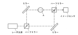
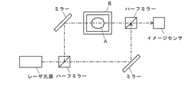
- Holographic observation apparatuses include those using a light beam reflected by the observation target object A as shown in FIG. 1 and those using a light beam transmitted through the observation target object A as shown in FIG. 2 (Non-patent Document 2).
- Non-patent Document 2 when the coherent light beam from the light source is reflected or transmitted by the observation target object A, it undergoes a phase change according to the optical structure of the observation target object A.
- a hologram is obtained by causing the light beam that has undergone the phase displacement and the reference light beam that has not undergone such a phase displacement to interfere with each other on the image sensor.
- FIG. 3 there are various objects in addition to the object to be observed on the optical path for observation.
- the cell when observing a cell alive, the cell is suspended in a medium in a container or placed on a glass plate, and in this case, the observation target object is placed on the optical path.
- the observation target object In addition to the cells, there are containers and glass plates. Since the phase displacement of the coherent beam is generated not only by the observation target object but also by other objects on the optical path, interference due to the phase displacement generated by the non-observation target object B (a container or the like in the previous example) in FIG.
- the interference image generated by the observation target object A (cell) and caused by the originally required phase shift is affected, image noise is generated, and the image quality of the hologram of the observation target object A is deteriorated. Therefore, in order to obtain a good observation image, the influence of the phase displacement generated by an object other than the observation target object (non-observation target object) is eliminated as much as possible, and only the interference image generated from the phase displacement generated by the observation target object is obtained. It is desirable to detect.
- the problem to be solved by the present invention is to provide a holographic observation method and apparatus capable of obtaining a hologram with a resolution as high as possible only for the observation target object by suppressing the influence of the phase displacement other than the observation target object. is there.
- the holographic observation method according to the present invention made to solve the above problems is as follows.
- An object to be observed is irradiated with a light beam generated by driving a semiconductor laser light source with a current superimposed with an alternating current component, or a light beam having a predetermined spectral width and a predetermined spectral intensity and having a predetermined coherency,
- a hologram is formed by causing a light beam transmitted or reflected through an observation target object to interfere with a reference light beam, and information on the observation target object is obtained by performing image processing on the hologram.
- a semiconductor laser light source When a semiconductor laser light source is driven by a current superimposed with an AC component, it is generated by driving the semiconductor laser light source with a constant DC current that has a spectrum width corresponding to the amplitude and frequency of the superimposed AC component and has no fluctuations. Light with lower coherency than that of a semiconductor laser beam can be obtained.
- a super luminescent diode (SLD) light source also has a predetermined spectral width and a predetermined spectral intensity, and is less coherent than a semiconductor laser beam generated by driving a semiconductor laser light source with a direct current. A luminous flux is obtained.
- SLD super luminescent diode
- the light beam having the predetermined spectral width and the predetermined spectral intensity and having the predetermined coherency means a light beam emitted from such a light source such as an SLD light source.
- a hologram is formed using a coherent light beam having a small spectral width (that is, a single wavelength) as generated from a semiconductor laser light source driven by a direct current, even if it is far from the light source that emits the coherent light beam Since coherency is maintained, interference with the reference light can occur over a long distance (the coherence distance is long).
- a light beam having a predetermined coherence by having a predetermined spectral width and a predetermined spectral intensity used in the present invention has a shorter coherence distance as the coherence is lower. Therefore, it becomes possible to reflect (include) only the result of the phase displacement of the observation target object in the hologram and not reflect (exclude) the result of the phase displacement by the other non-observation target object.
- pseudo-coherent light having a predetermined coherency by having a predetermined spectral width and a predetermined spectral intensity is also referred to as pseudo-coherent light.
- the pseudo-coherent light used in the present invention is sometimes called low-coherent light in contrast to high-coherent light such as semiconductor laser light.
- Each of the predetermined spectral width and the predetermined spectral intensity has appropriate values depending on the size and optical characteristics of the object to be observed, and can be easily determined by conducting an experiment in advance. An example will be described later.
- one of the methods for forming a light beam (pseudo-coherent light beam) used in the present invention uses a semiconductor laser diode (semiconductor laser) as a semiconductor laser light source, and superimposes an AC signal on a current source that drives the semiconductor laser diode.
- the semiconductor laser diode is basically driven with a constant direct current.
- a light beam having a very narrow spectral width and high coherency is obtained (FIG. 4A).
- an alternating current is superimposed on the driving direct current, the spectrum of the generated light beam has a width under certain conditions.
- the aspect of this spectrum varies depending on the frequency of the alternating current component to be superimposed.
- the frequency of the AC component to be superimposed is a high frequency of about 100 MHz to 500 MHz
- the spectrum appears to spread discretely as shown in FIG. 4 (b1) (Patent Documents 1 and 2).
- the reason why such a spectrum spread is formed is considered as follows. That is, even when a semiconductor laser diode of a single mode laser is driven with a constant direct current as usual, immediately after the current starts flowing (about several nanoseconds after the current starts flowing) , ⁇ 1st order, ⁇ 2nd order side mode light emission occurs (that is, a multimode light emission state is formed), and as a result, it spreads discretely as shown in FIG.
- the frequency of the superimposed AC component is a low frequency of about 50 kHz to 300 kHz, it has been confirmed that the emission wavelength varies with time. Such fluctuations are considered to occur due to temporal fluctuations in the current, the refractive index inside the resonator, the temperature distribution, and the like due to the superposition of low-frequency AC components. If the frequency of the superimposed alternating current component is sufficiently higher (preferably about 1000 times) than the readout frequency of the image sensor (that is, the image sensor that acquires the interference image of the light beam transmitted or reflected through the observation object) The period of fluctuation is averaged over time at the time of imaging, and it can be considered that the peak width of the spectrum is widened (a broad spectrum is obtained).
- the spread mode differs between the high-frequency alternating current component and the low-frequency alternating current component, so that the spectrum width can be effectively broadened by combining both. That is, in a semiconductor laser diode that emits light having a discretely spread spectrum distribution as shown in FIG. 4 (b1) by being driven by a current superimposed with a high-frequency alternating current component, When the low-frequency alternating current component is further superimposed, the peak width of each discrete peak spreads, and as a result, the spectrum appears to continuously spread as shown in FIG. 4 (c). Become. Thus, the spectrum width can be sufficiently widened by superimposing both the high-frequency AC component and the low-frequency AC component.
- the method of obtaining a light beam having a discretely spread spectrum from a semiconductor laser diode exhibiting a spectrum as shown in FIG. 4A is limited to a method in which a high-frequency AC component is superimposed on a drive current. Absent. In other words, a part of the light emitted from the semiconductor laser diode is reflected back to the semiconductor laser diode by reflecting the light using, for example, an optical component (that is, the return light is formed). Can be obtained. In this configuration, a resonance state is formed between the semiconductor laser diode and the optical component (that is, a resonator is formed not only inside but also outside the semiconductor laser diode). As a result, the semiconductor laser diode has different oscillation frequencies inside and outside, and as a result, multimode oscillation occurs and exhibits a discretely spread spectrum as shown in FIG. 4 (b2). It is thought that it will become.
- the return light can be formed, for example, by disposing a reflecting member having a reflecting surface that reflects at least a part of the incident light on the optical axis of the light emitted from the semiconductor laser.
- the amount of return light can be controlled by the angle of the reflecting member (the angle formed by the reflecting surface and the optical axis).
- the laser resonator gain, loss, current operating point of the semiconductor laser, the Fresnel reflectivity of the end faces of the semiconductor laser and the optical fiber, the matching with the laser resonator by the return light, etc. may be affected. Since there is a possibility, it is preferable to determine the optimum value of the return light by adjustment by a combination of the angle of the reflecting member and a parameter that affects the reflection member.
- a light beam having a predetermined coherent property can be obtained by having the predetermined spectral width and the predetermined spectral intensity.
- the spectral width of the pseudo-coherent light beam can be sufficiently widened.
- the spectrum width of the pseudo-coherent light beam can be widened by increasing the amplitude of the superimposed alternating current component.
- a light beam having a predetermined coherent property by having the predetermined spectral width and the predetermined spectral intensity can also be obtained by using, for example, a super luminescent diode (SLD). Can do. Further, some light emitting diodes (LEDs) having such characteristics can also be used as the light source of the holographic observation device according to the present invention. SLDs and some LEDs emit light having a predetermined spectral width and a shorter coherence distance than laser light.
- SLD super luminescent diode
- the spectral width and coherence distance of light emitted from an SLD or LED are fixed, so it is necessary to select an SLD or LED that matches the coherence distance determined according to the size and optical characteristics of the object to be observed.
- the holographic observation apparatus can be configured simply and inexpensively.
- one aspect of a holography observation device using the method according to the present invention is: a) a semiconductor laser light source; b) a current source for supplying a driving current in which an AC component is superimposed on the semiconductor laser light source; c) an irradiation optical system that transmits or reflects a light beam emitted from the semiconductor laser light source driven by the drive current to an observation target object, and interferes with light transmitted or reflected at different positions of the observation target object; d) An image sensor that acquires an interference image of a light beam transmitted or reflected through the observation object.
- another aspect of the holographic observation apparatus using the method according to the present invention is: a) a light source that emits a light beam having a predetermined coherency by having a predetermined spectral width and a predetermined spectral intensity; b) an irradiation optical system that transmits or reflects the light flux to the observation target object and interferes with the light transmitted or reflected at different positions of the observation target object; c) An image sensor that acquires an interference image of a light beam transmitted or reflected by the observation object.
- one aspect of the holographic observation device is: a) a semiconductor laser light source; b) a current source for supplying a current with an alternating current component superimposed on the semiconductor laser light source; c) an irradiation optical system that divides the light beam emitted from the semiconductor laser light source driven by the drive current into two parts, and transmits or reflects one of the light beams to the observation object; c) An image sensor that acquires an interference image between a light beam that has been transmitted or reflected through the observation target object and a light beam that is the other of the two light beams that has not been transmitted or reflected through the observation target object.
- another aspect of the holographic observation device is: a) a light source that emits a light beam having a predetermined coherency by having a predetermined spectral width and a predetermined spectral intensity; b) an irradiation optical system that divides the luminous flux into two and transmits or reflects one of them to the object to be observed; c) An image sensor that acquires an interference image between a light beam that has been transmitted or reflected through the observation target object and a light beam that is the other of the two light beams that has not been transmitted or reflected through the observation target object.
- any of these types of holographic observation devices is as described above, and only the result of phase displacement in the observation target object is reflected by using a quasi-coherent light beam with a short coherence distance (information on the observation target object).
- Holograms that do not include (do not include) the phase displacement results of other objects As described above, for example, a superluminescent diode (SLD) or a light beam having a predetermined spectral width is used as a light source that emits a light beam having a predetermined spectral width and a predetermined spectral intensity and having a predetermined coherency.
- SLD superluminescent diode
- Some of the generated light emitting diodes (LEDs) can be used.
- the present invention is also directed to a cell image observation apparatus provided with each of the above holographic observation apparatuses, and a light source unit suitably used for, for example, each of the above holography observation apparatuses.
- a pseudo-coherent light beam having a predetermined coherent property by having a predetermined spectral width and a predetermined spectral intensity and having a short coherent distance is used as the observation light beam.
- FIG. 1 shows a configuration example of an off-axis holography observation apparatus using reflected light from an observation object.
- 1 shows a configuration example of an off-axis holography observation apparatus that uses transmitted light from an observation object.
- An emission spectrum when the semiconductor laser light source is driven with a direct current (a) an emission spectrum when the high-frequency alternating current signal is superimposed on the drive current of the semiconductor laser light source (b1), and a return light to the semiconductor laser light source Emission spectrum (b2), and emission spectrum (c) when a low-frequency AC signal is superimposed on the driving current of the semiconductor laser light source.
- mold holography observation apparatus which is one Example of the holography observation apparatus which concerns on this invention.
- the principal part block diagram of the off-axis type holography observation apparatus which is a modification of the holography observation apparatus which concerns on this invention.
- the holographic observation apparatus of the present embodiment is a so-called inline holography observation apparatus (refer to Non-Patent Documents 1 and 2 for the inline holography observation apparatus), and the cells such as iPS cells and ES cells cultured on the culture plate. Used to acquire an observation image.
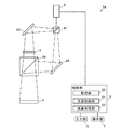
- FIG. 5 shows the main configuration of the holographic observation apparatus of this example.
- the holographic observation device 1 includes a light source unit 2, an image sensor 4, and a control unit 5.
- a pseudo-coherent light beam having a small angle (about 10 degrees) emitted from the light source unit 2 is irradiated to cells on the culture plate 3.
- the light in the pseudo-coherent light beam transmitted through the cells and the culture plate 3 reaches the image sensor 4 while interfering with the light transmitted through the adjacent position of the cells on the culture plate 3.
- an appropriate irradiation optical system is used to irradiate the entire cell with the spot size of the light beam emitted from the light source unit 2.
- the control unit 5 includes a storage unit 50, and also includes a light source control unit 51 that controls the operation of the light source unit 2 as a functional block, and an arithmetic processing unit 52.
- the arithmetic processing unit 52 obtains phase information by numerical calculation from hologram data acquired by the image sensor 4 (two-dimensional intensity distribution data of the pseudo-coherent light beam formed on the detection surface of the image sensor 4), and obtains an observation image of the cell.
- An arithmetic processing unit 52 is provided.
- the storage unit 50 is information related to the relationship between the magnitude of the current supplied to the semiconductor laser diode 24 and the intensity of the pseudo-coherent light beam, and the relationship between the amplitude and frequency of the AC signal and the coherent distance of the pseudo-coherent light beam.
- Pseudo-coherent light flux characteristic information is stored in advance. The relationship between the amplitude and frequency of the AC signal and the coherent distance of the pseudo-coherent light beam will be described later.
- An input unit 6 and a display unit 7 are connected to the control unit 5. The observation image created by the arithmetic processing unit 52 is displayed on the display unit 7.
- the light source unit 2 includes a semiconductor laser diode 24 and a drive current supply unit 20 that supplies a drive current to the semiconductor laser diode 24.
- the drive current supply unit 20 includes a DC voltage generation unit 21 that generates a DC voltage, an AC voltage generation unit 22 that generates an AC voltage and superimposes the AC voltage on the DC voltage, and a voltage / current conversion unit 23.
- the light source control unit 51 determines the magnitude of the DC voltage generated by the DC voltage generation unit 21 based on a user input instruction regarding the intensity and coherence distance of the pseudo coherent light beam and the pseudo coherent light beam characteristic information stored in the storage unit 50. And the intensity of the semiconductor laser beam is adjusted, and the amplitude and frequency values of the AC voltage generated by the AC voltage generator 22 are determined to adjust the coherence distance of the semiconductor laser beam.
- the holography observation apparatus 1 of this embodiment observes the cells on the culture plate 3.
- the light source control unit 51 is based on the quasi-coherent light flux characteristic information.
- the coherence distance of the generated pseudo-coherent light beam is longer than the thickness of the observation target object (cell) (for example, several tens to one hundred ⁇ m), and the non-observation target object (culture plate 3) existing on the optical path
- the amplitude and frequency of the AC signal are determined so as to be shorter than the thickness (for example, about 1 mm).
- this frequency is set to a frequency sufficiently higher than the signal readout cycle of the image sensor 4 (for example, a frequency 1000 times the signal readout frequency of the image sensor 4).
- the thickness of the culture plate 3 is input.
- a container, a glass plate, or the like that contains the sample is present on the optical path.
- the user also enters their thickness.
- the thickness of the thinnest object among the non-observation target objects is input.
- only the thickness of the cell and the culture plate 3 is input.
- the refractive index is also input. It is preferable that the coherent distance of the pseudo-coherent light beam is longer than the optical thickness (product of the physical thickness and the refractive index) of the observation target object and shorter than the optical thickness of the non-observation target object.
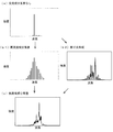
- FIG. 7A shows a measurement result indicating a coherent distance when the semiconductor laser diode is driven only by a direct current.
- the horizontal axis in the figure indicates the distance from the semiconductor laser light emitting end toward the left, and the vertical axis indicates the amplitude (interference intensity) at the distance.
- the measurement is only performed at a distance of about 8 cm from the emitting end of the semiconductor laser beam, but since a sufficiently large interference peak can be confirmed up to this distance, the coherence distance is about several meters. It is thought that there is.
- FIG. 7B is a diagram showing a coherent distance when an AC signal (frequency 100 kHz, amplitude 30% with respect to DC) is superimposed on the driving current of the semiconductor laser diode, and FIG. It is an enlarged view of the vicinity of the emission end.
- the coherence distance is reduced to about 4 mm from the emission end of the semiconductor laser beam, and the interference intensity is greatly reduced and most of the peaks due to the interference disappear.
- the coherence distance of the semiconductor laser beam becomes shorter as the amplitude of the AC signal superimposed on the drive current of the semiconductor laser diode increases. It was confirmed that This is presumably because the spectral width of the light beam increases as the amplitude of the superimposed alternating current signal increases, and as a result, the coherency decreases and the coherence distance decreases.
- the frequency of the AC signal superimposed on the drive current is a frequency that can modulate the semiconductor laser light with a period sufficiently shorter than the signal readout period of the image sensor 4 (that is, sufficiently higher than the signal readout frequency of the image sensor 4). (High frequency), and is particularly preferably about 1000 times the signal readout frequency of the image sensor 4.
- the signal readout cycle is 33 ms (readout frequency 30 Hz), and thus the above-described low-frequency AC signal of 50 kHz to 300 kHz can be used satisfactorily.
- FIG. 8A is an observation image of only the culture plate 3 (no medium or cells) obtained by irradiating a 642 nm coherent light beam by a conventional holographic observation method (apparatus). In this observation image, it can be seen that unnecessary interference fringes due to the phase displacement of the culture plate 3 are superimposed over the entire image.
- FIG. 8B shows a holographic observation method (apparatus) according to the present embodiment in which the semiconductor laser diode is superimposed on a DC voltage by superimposing an AC voltage having a frequency of 100 kHz and an amplitude (amplitude of driving DC current) of 24% on the DC voltage. It is an observation image of only the culture plate 3 (without medium or cells), which was obtained by driving and irradiating a pseudo-coherent light beam having a center spectrum of 642 nm. In both of FIGS. 8A and 8B, an image sensor having a readout cycle of 33 ms (a readout frequency of 30 Hz) was used. In the observation image of FIG. 8B, it can be seen that unnecessary interference fringes due to the culture plate 3 are greatly reduced.
- the frequency of the AC component superimposed on the drive current (specifically, the frequency of the AC voltage superimposed on the DC voltage) is not limited to a low frequency of 50 kHz to 300 kHz.
- a high frequency alternating current component of 1 MHz to several hundred MHz (preferably 100 MHz to 500 MHz) may be superimposed, or both of these low frequency components and high frequency components may be superimposed.
- a general semiconductor laser diode that oscillates in a single mode often exhibits an emission spectrum of the type shown in FIG. 4A when driven by a direct current.
- a semiconductor laser diode is driven with a current superimposed with an alternating current component of a high frequency of 100 MHz to 500 MHz, the emission spectrum thereof is as shown in FIG. 4 (b1).
- the emission spectrum appears to spread discretely.
- a low-frequency AC component of about 50 kHz to 300 kHz is superimposed on the drive current (that is, a high frequency of 100 MHz to 500 MHz).
- the alternating current component with a frequency component and a low frequency component of 50 kHz to 300 kHz is superimposed
- the peak width of each discrete peak spreads, and its emission spectrum is as shown in FIG. It will appear to spread continuously.
- the spectrum width can be sufficiently widened by superimposing the alternating current component on which the high frequency component and the low frequency component are superimposed on the drive current.
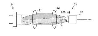
- FIG. 9 shows a configuration example of the light source unit 2a according to another method.
- the light emitted from the semiconductor laser diode 24 is collimated by the collimator lens 81, collected by the focus lens 82 on the ferrule 83, and guided by the optical fiber 84.
- the cells on the culture plate 3 are irradiated (see FIG. 5).
- the ferrule 83 has a tip formed by a reflection surface 830 that reflects a part of incident light, and the reflection surface 830 is disposed on the optical axis of the light emitted from the semiconductor laser diode 24.
- the reflecting surface 830 is disposed in such a posture that the normal line and the optical axis form a predetermined angle ⁇ that is not zero. That is, they are arranged in such a posture that the normal line of the reflecting surface 830 and the optical axis do not coincide.
- the predetermined angle ⁇ is an angle at which a part of the light reflected by the reflecting surface 830 returns to the semiconductor laser diode 24 (that is, return light is formed).
- the smaller the angle ⁇ the more light returns to the semiconductor laser diode 24.
- the semiconductor laser diode 24 may be damaged by the return light.
- the angle ⁇ increases, the amount of light returning to the semiconductor laser diode 24 decreases.
- no light returns to the semiconductor laser diode 24.
- 10 to 90% of the light emitted from the semiconductor laser diode 24 can be returned to the semiconductor laser diode 24. .
- the laser resonator gain, loss, current operating point of the semiconductor laser diode 24, Fresnel reflectivity of the end faces of the semiconductor laser diode 24 and the optical fiber 84, and return light are determined.
- the reflecting surface 830 for forming the return light does not necessarily need to be configured by the tip of the ferrule 83.
- An optical component such as a mirror is provided separately from the ferrule 83, and the return light is formed by the mirror. Also good.
- the emission spectrum is as shown in FIG. 4 (b2). That is, by forming the return light, the spectrum appears to have a discrete spread.
- the spectrum width at this time changes according to the angle ⁇ described above. That is, an arbitrary spectral width can be formed by adjusting the angle ⁇ .
- FIG. 10 shows a main configuration of an off-axis holography observation apparatus 1a which is a modified example. Since the light source unit 2, the culture plate 3, the image sensor 4, the control unit 5, the input unit 6, and the display unit 7 are the same as those in the above embodiment, the same reference numerals are given and the description thereof is omitted.
- this holographic observation device 1a a measurement beam that irradiates a cell with a pseudo-coherent beam having a predetermined coherence distance by having a predetermined spectral width and a predetermined spectral intensity emitted from the light source unit 2 by a first half mirror 41. Then, it is divided into reference light fluxes that do not irradiate the cells.
- the measurement light beam reflected by the first half mirror 41 is reflected by the first mirror 42 and subsequently irradiated to the cells on the culture plate 3. Further, the reference light beam transmitted through the first half mirror 41 is reflected by the second mirror 45. The measurement light beam transmitted through the cell and the reference light beam reflected by the second mirror 45 are combined by the second half mirror 44 and interfere with each other, and are measured by the image sensor 4.
- the off-axis holographic observation apparatus 1a shown in FIG. 10 uses transmitted light, but the present invention can be applied to an apparatus using reflected light.
- the light source unit 2 having only one semiconductor laser diode 24 and the drive current supply unit 20 is used.
- a plurality of semiconductor laser diodes having different oscillation wavelengths and driving for driving each semiconductor laser diode are used. It is also possible to use a light source having a section or a plurality of SLDs and / or LEDs having different oscillation wavelengths.
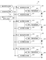
- FIG. 11 shows a configuration of the light source unit 2b when a plurality of semiconductor laser diodes having different oscillation wavelengths are used.
- the light source unit 2b includes four types of semiconductor laser diodes 241 to 244 that emit light having different wavelengths, and driving current supply units 201 to 204 that supply driving currents to the semiconductor laser diodes 241 to 244, respectively.
- the drive current supply units 201 to 204 respectively include DC voltage generation units 211 to 214 that generate a DC voltage, AC voltage generation units 221 to 224 that generate an AC voltage and superimpose the DC voltage, and a voltage / current Conversion units 231 to 234 are provided.
- the light source unit 2b further includes a DC signal generation unit 25 that generates a DC signal to be transmitted to the DC voltage generation units 211 to 214, an AC signal generation unit 26 that generates an AC signal to be supplied to the AC voltage generation units 221 to 224, and An illumination timing signal generator 27 that generates timing signals to be supplied to the DC voltage generators 211 to 214 is provided.
- a DC signal generation unit 25 that generates a DC signal to be transmitted to the DC voltage generation units 211 to 214
- an AC signal generation unit 26 that generates an AC signal to be supplied to the AC voltage generation units 221 to 224
- An illumination timing signal generator 27 that generates timing signals to be supplied to the DC voltage generators 211 to 214 is provided.
- the (average) intensity of the pseudo-coherent luminous flux emitted from each of the semiconductor laser diodes 241 to 244 is controlled by the magnitude of the DC signal transmitted from the DC signal generating unit 25 to each of the DC voltage generating units 211 to 214. To do. Further, the coherent distance of the pseudo-coherent light beam emitted from each of the semiconductor laser diodes 241 to 244 is controlled by the frequency and amplitude of the AC signal transmitted from the AC signal generator 26 to each of the AC voltage generators 212 to 224.
- the frequency of the AC signal is set to a frequency that is sufficiently higher than the readout frequency of the image sensor (for example, about 1000 times the frequency), and the coherence distance is appropriate depending on the size and optical characteristics of the object to be observed.
- the length (for example, several hundred ⁇ m) is set.
- the illumination timing signal generation unit 27 transmits timing signals to the semiconductor laser diodes 241 to 244 in order.
- the drive current supply units 201 to 204 when the timing signal is transmitted to the DC voltage generation units 211 to 214, the DC signal generated by the DC voltage generation units 211 to 214 is generated by the AC signal generation units 221 to 224.
- the alternating current signal is superimposed and transmitted to the voltage / current converters 231 to 234, and the drive current is supplied to the semiconductor laser diodes 241 to 244.
- the observation target object is sequentially irradiated with pseudo-coherent light beams having different wavelengths, and a holographic image of the observation target object by the pseudo-coherent light beams of the respective wavelengths is obtained.
- the interference mode of the pseudo-coherent light beam irradiated to the object to be observed varies depending on the wavelength of the light beam. Therefore, the four types of quasi-coherent light beams having different wavelengths are irradiated onto the observation target object as described above, and four types of holographic images that differ according to the wavelength can be obtained. By reconstructing the image of the object to be observed using the four types of holographic images thus obtained, it is possible to obtain an image of the object to be observed with a higher resolution than when only one type of light beam is used.
Landscapes
- Physics & Mathematics (AREA)
- General Physics & Mathematics (AREA)
- Electromagnetism (AREA)
- Condensed Matter Physics & Semiconductors (AREA)
- Optics & Photonics (AREA)
- Theoretical Computer Science (AREA)
- Computing Systems (AREA)
- Engineering & Computer Science (AREA)
- Holo Graphy (AREA)
- Investigating Or Analysing Materials By Optical Means (AREA)
- Microscoopes, Condenser (AREA)
- Length Measuring Devices By Optical Means (AREA)
- Semiconductor Lasers (AREA)
Abstract
交流成分を重畳した電流により半導体レーザ光源を駆動することにより生成した光束、又は所定のスペクトル幅及び所定のスペクトル強度を有することで所定のコヒーレント性を有する光束を観察対象物体に照射し、観察対象物体を透過又は反射した光束と、参照光束とを干渉させることによりホログラムを形成し、該ホログラムを画像処理することにより観察対象物体に関する情報を得ることを特徴とするホログラフィ観察方法。例えば、所定のスペクトル幅及び所定のスペクトル強度を有することで所定のコヒーレント性を有する光束を発する光源2と、該光束を2分割し、双方を観察対象物体に透過又は反射させる照射光学系2と、観察対象物体を透過又は反射した光束の干渉像を取得するイメージセンサ4とを備える、インライン型のホログラフィ観察装置1を用いる。
Description
本発明は、ホログラフィを用いて対象物体を観察する方法及び装置に関する。
iPS細胞を用いた再生医療技術等の進展に伴い、iPS細胞やその他の細胞を培養しつつ、それら細胞を観察し、細胞の分化状態等を適切に管理するための装置が求められるようになっている。そのような装置では、培養の過程で細胞の画像を取得し、その画像データに基づいて様々な計測及び解析を行う必要がある。細胞の観察を行う装置としては、位相差顕微鏡を用いて観察する装置があるが、1回に撮影できる領域が限られるため、全体を観察するためにはステップ・アンド・リピート方式で撮影位置を変えながら全体観察を行う必要がある。そうすると、撮影位置を移動する度に対象物に焦点を合わせる必要があり、全体の撮影に時間がかかるという問題がある。培養細胞の観察においては、細胞にダメージを与えないために、撮影はできるだけ短時間に済ませる必要がある。
そこで、ホログラフィを用いて細胞の撮影を行うホログラフィ観察装置が広く用いられるようになってきた。ホログラフィ画像(ホログラム)は、位相の揃った光束(コヒーレント光束)を2つに分割し、一方を対象物体に照射して通過又は反射させ、他方をそのままにして、両光束を結像面で干渉させることにより得られる。こうして得られたホログラムには対象物体の3次元的形状や光学的組成等の情報が含まれており、これに対して各種演算を行うことによりそれらを取り出すことができる。ホログラフィ観察装置では、撮影時に得た対象物体の3次元データを元に、画像再構成時に焦点合わせを行った対象物体付近の2次元画像データを得ることができ、撮影時の焦点合わせが不要であるため、上記位相差顕微鏡を用いる場合に比べて高速な全体観察が可能になるという特長を有している。なお、本願明細書において「光束」という文言は断面が2次元的な広がりを持つ光を意味する。
ホログラフィ観察装置は、図1に示すように観察対象物体Aで反射した光束を用いるものと、図2のように観察対象物体Aを透過した光束を用いるものがある(非特許文献2)。いずれのタイプのものでも、光源からのコヒーレント光束は観察対象物体Aで反射され、又は透過する際に、その観察対象物体Aの光学的構造に応じた位相の変化を受ける。このように位相変位を受けた光束と、そのような位相変位を受けない参照光束をイメージセンサ上で干渉させることにより、ホログラムが得られる。
R. Stahl, et. al., "Lens-free digital in-line holographic imaging for wide field-of-view, high resolution and al-time monitoring of complex microscopic objects", Proc. of SPIE Vol. 8947
粟辻安浩, "並列ディジタルホログラフィック顕微鏡法による細胞の3次元動画像計測法及びその装置の開発", 堀場製作所 Readout (35), 10-15, 2009-12 (2009)
図3に模式的に示すように、観察を行う光路上には、観察対象物体の他に様々な物体が存在する。例えば、細胞を生きたまま観察しようとする場合、細胞を容器内で培地中に浮遊させたり、ガラス板上に載置したりして観察を行うが、この場合、光路上には観察対象物体である細胞の他に、容器やガラス板等が存在する。コヒーレント光束の位相変位は観察対象物体だけでなく、光路上にある他の物体によっても発生するため、図3において非観察対象物体B(先の例では容器など)によって発生した位相変位による干渉が、観察対象物体A(細胞)により発生する、本来必要とされる位相変位から生じる干渉像に影響を及ぼすと画像ノイズが生じ、観察対象物体Aのホログラムの画質を劣化させることとなる。そのため、良好な観察画像を得るためには、観察対象物体以外の物体(非観察対象物体)によって発生する位相変位の影響をできるだけ排除し、観察対象物体によって発生する位相変位から生じる干渉像のみを検出することが望ましい。
本発明が解決しようとする課題は、観察対象物体以外での位相変位の影響を抑制して、観察対象物体のみについてできるだけ解像度の高いホログラムを得ることのできるホログラフィ観察方法及び装置を提供することである。
上記課題を解決するために成された本発明に係るホログラフィ観察方法は、
交流成分を重畳した電流により半導体レーザ光源を駆動することにより生成した光束、又は、所定のスペクトル幅及び所定のスペクトル強度を有することで所定のコヒーレント性を有する光束を、観察対象物体に照射し、観察対象物体を透過又は反射した光束と、参照光束とを干渉させることによりホログラムを形成し、該ホログラムを画像処理することにより観察対象物体に関する情報を得ることを特徴とするものである。
交流成分を重畳した電流により半導体レーザ光源を駆動することにより生成した光束、又は、所定のスペクトル幅及び所定のスペクトル強度を有することで所定のコヒーレント性を有する光束を、観察対象物体に照射し、観察対象物体を透過又は反射した光束と、参照光束とを干渉させることによりホログラムを形成し、該ホログラムを画像処理することにより観察対象物体に関する情報を得ることを特徴とするものである。
交流成分を重畳した電流により半導体レーザ光源を駆動すると、重畳される交流成分の振幅及び周波数に応じたスペクトル幅を有し、変動のない一定の直流電流で半導体レーザ光源を駆動することにより生成される半導体レーザ光束に比べてコヒーレント性の低い光が得られる。また、スーパールミネッセントダイオード(SLD)光源からも、所定のスペクトル幅及び所定のスペクトル強度を有し、直流電流で半導体レーザ光源を駆動することにより生成される半導体レーザ光束よりもコヒーレント性が低い光束が得られる。上記所定のスペクトル幅及び所定のスペクトル強度を有することで所定のコヒーレント性を有する光束とは、このようなSLD光源等の光源から発せられる光束をいう。直流電流で駆動される半導体レーザ光源から生成されるようなスペクトル幅の小さい(すなわち、単一波長の)コヒーレント光束を用いてホログラムを形成する場合、該コヒーレント光束を発する光源から遠くであってもコヒーレント性は保持されるため、長い距離に亘って参照光との干渉が生じ得る(可干渉距離が長い)。従って、観察対象物体のみならず、それ以外の非観察対象物体(例えば、細胞を観察しようとする場合、それを収容する容器、その容器の蓋およびその他の光学部品、等)による位相変位の結果もホログラムに含まれるようになる。それに対し、本発明において用いる所定のスペクトル幅及び所定のスペクトル強度を有することで所定のコヒーレンス性を有する光束は、そのコヒーレンス性が低いほど可干渉距離が短くなる。そのため、観察対象物体における位相変位の結果のみをホログラムに反映させ(含め)、それ以外の非観察対象物体による位相変位の結果を反映させない(含めない)ようにすることができるようになる。なお、本願明細書では、このように所定のスペクトル幅及び所定のスペクトル強度を有することで所定のコヒーレント性を有する光を擬コヒーレント光とも呼ぶ。本発明において用いる擬コヒーレント光は、半導体レーザ光のような高コヒーレント光との対比で低コヒーレント光と呼ばれることもある。
上記所定のスペクトル幅及び所定のスペクトル強度の各々は、観察対象物体の大きさや光学的特性に応じて適切な値が存在するが、それは予め実験を行うことにより容易に決定することができる。なお、一例は後述する。
上述のとおり、本発明において用いる光束(擬コヒーレント光束)を形成する方法の一つは、半導体レーザ光源として半導体レーザダイオード(半導体レーザ)を使用し、それを駆動する電流源に交流信号を重畳する方法である。シングルモードレーザの場合、半導体レーザダイオードは基本的に一定の直流電流で駆動するが、その場合、スペクトル幅の非常に狭い、コヒーレント性の高い光束が得られる(図4(a))。それに対し、その駆動直流電流に交流電流を重畳すると、一定の条件下で、発生する光束のスペクトルは幅を持つようになる。
このスペクトルの様相は、重畳する交流成分の周波数により異なる。例えば、重畳する交流成分の周波数が、100MHz~500MHz程度の高周波数である場合、図4(b1)に示すように、スペクトルが離散的に広がった様相を呈する(特許文献1、2)。このようなスペクトルの広がりが形成される理由は次のように考えられる。すなわち、シングルモードレーザの半導体レーザダイオードは、通常通り一定の直流電流で駆動した場合であっても、電流が流れ始めた直後(電流が流れ始めてから数ナノ秒間程度)は、中心モードによる発光と、±1次、±2次のサイドモードによる発光が生じており(すなわち、マルチモードの発光状態が形成されており)、その結果、図4(b1)に示されるような離散的に広がったスペクトル分布となる。しかし、一定の直流電源で駆動し続けると、サイドモードはすぐに減衰して中心モードのみによる発光(縦モードシングル発光)だけが残った状態となる。一方、このようなシングルモードレーザの半導体レーザダイオードを、100MHz~500MHz程度の高周波数の交流成分を重畳した電流で駆動した場合、半導体レーザダイオードが縦モードシングル発光の状態で安定する前に電流が変化するため、サイドモードによる発光が維持され、結果として、図4(b1)に示されるように離散的に広がったスペクトル分布での発光が維持されることになる。
一方、重畳する交流成分の周波数が、50kHz~300kHz程度の低周波数である場合、発光波長が時間的に変動することが確認されている。このような変動は、低周波数の交流成分が重畳されることにより、電流、共振器内部の屈折率、温度分布、等が時間的に変動することに起因して起こるものと考えられる。重畳される交流成分の周波数が、イメージセンサ(すなわち、観察対象物体を透過又は反射した光束の干渉像を取得するイメージセンサ)の読み出し周波数よりも十分大きい(好ましくは、1000倍程度)場合、この変動の周期は撮影の際に時間的に平均され、スペクトルのピーク幅が広がる(ブロードなスペクトルが得られる)とみなすことができる。
このように、高周波数の交流成分あるいは低周波数の交流成分のどちらであっても、それを重畳することでスペクトル幅を広げることが可能である。ただし、上記の通り、その広がりの態様は高周波数の交流成分と低周波数の交流成分で異なるため、両者を組み合わせることでスペクトル幅を効果的に広げることができる。すなわち、高周波数の交流成分を重畳した電流で駆動されることにより図4(b1)に示されるような離散的に広がったスペクトル分布の発光を形成している半導体レーザダイオードにおいて、その駆動電流に、低周波数の交流成分をさらに重畳すると、離散的に存在する各ピークのピーク幅が広がり、結果として、スペクトルは、図4(c)に示すように、連続的に広がった様相を呈するようになる。このように、高周波数の交流成分と低周波数の交流成分の両方を重畳することで、スペクトル幅を十分に広げることができる。
ここで、図4(a)に示されるようなスペクトルを呈している半導体レーザダイオードから、離散的に広がったスペクトルの光束を得る手法は、駆動電流に高周波数の交流成分を重畳するものに限らない。すなわち、半導体レーザダイオードから出射される光の一部を、例えば光学部品等を用いて反射させることにより半導体レーザダイオードに戻す(すなわち、戻り光を形成する)ことによっても、半導体レーザダイオードから離散的に広がったスペクトルの光束を得ることができる。この構成においては、半導体レーザダイオードと該光学部品の間に共振状態が形成される(すなわち、半導体レーザダイオードの内部だけでなく外部にも共振器が形成される)。これによって、半導体レーザダイオードは、その内部と外部で異なる発振周波数を有するものとなり、その結果、マルチモードでの発振が生じ、図4(b2)に示されるような離散的に広がったスペクトルを呈するようになると考えられる。
戻り光は、例えば、半導体レーザから出射される光の光軸上に、入射した光の少なくとも一部を反射させる反射面を有する反射部材を配置することにより形成することができる。ここにおいて、該反射部材の角度(反射面と光軸がなす角度)によって、戻り光の光量を制御することができる。ただし、戻り光の光量によっては、半導体レーザのレーザ共振器ゲイン、損失、電流動作点、半導体レーザおよび光ファイバの端面のフレネル反射率、戻り光によるレーザ共振器とのマッチング、等に影響が生じる可能性があるため、該反射部材の角度とこれら影響をうけるパラメータとの組合せによる調整により、戻り光の最適値を決定することが好ましい。
戻り光が形成されることにより図4(b2)に示されるような離散的に広がったスペクトル分布の発光を形成している半導体レーザダイオードにおいて、その駆動電流に、低周波数の交流成分を重畳すると、離散的に存在する各ピークのピーク幅が広がり、結果として、スペクトルは、図4(c)に示すように、連続的に広がった様相を呈するようになる。この構成によると、高周波数の交流成分を重畳しなくともスペクトル幅を十分に広げることができるので、高周波数の交流成分を得るための複雑な回路構成や高価な部品が不要となる。
以上の通り、交流成分を重畳した電流で半導体レーザ光源を駆動することで、前記所定のスペクトル幅及び所定のスペクトル強度を有することで所定のコヒーレント性を有する光束(擬コヒーレント光束)が得られるところ、重畳する交流成分の周波数を適宜に選択することによって、擬コヒーレント光束のスペクトル幅を十分に広げることができる。また、重畳する交流成分の振幅を大きくすることによっても、擬コヒーレント光束のスペクトル幅を広げることができる。スペクトル幅が広がると、コヒーレント性が低下して可干渉距離が短くなる。従って、観察対象物体、及び光路上に存在する非観察対象物体の大きさ(厚さ)や光学的特性(例えば屈折率)に合わせて重畳する交流信号の周波数及び振幅を適宜に変更することにより、容器等による位相変位の影響を排除し、観察対象物体による位相変位のみをホログラムに反映させることができるようになる。
また、前記所定のスペクトル幅及び所定のスペクトル強度を有することで所定のコヒーレント性を有する光束(擬コヒーレント光束)は、上述のとおり、例えばスーパールミネッセントダイオード(SLD)を用いることによっても得ることができる。また、そのような特性を持つ一部の発光ダイオード(LED)も本発明に係るホログラフィ観察装置の光源として用いることができる。SLDや一部のLEDは、所定のスペクトル幅を有し、レーザ光に比べて可干渉距離が短い光を発する。一般にSLDやLEDから発せられる光のスペクトル幅や可干渉距離は固定であるため、観察対象物体の大きさや光学的特性に応じて決められる可干渉距離に合致するSLDやLEDを選択する必要はあるものの、交流信号を重畳する必要がなく光源から発せられる光をそのまま使用することができるため、ホログラフィ観察装置を簡素かつ安価に構成することができる。
本発明に係る方法は、ホログラフィを形成する方法に依らず適用することができる。
例えば、インライン型ホログラフィの場合、本発明に係る方法を用いたホログラフィ観察装置の一態様は、
a) 半導体レーザ光源と
b) 前記半導体レーザ光源に交流成分を重畳した駆動電流を供給する電流源と、
c) 前記駆動電流により駆動された前記半導体レーザ光源から発せられる光束を観察対象物体に透過又は反射させ、該観察対象物体の異なる位置で透過又は反射した光を干渉させる照射光学系と、
d) 前記観察対象物体を透過又は反射した光束の干渉像を取得するイメージセンサと
を備えるものとなる。
例えば、インライン型ホログラフィの場合、本発明に係る方法を用いたホログラフィ観察装置の一態様は、
a) 半導体レーザ光源と
b) 前記半導体レーザ光源に交流成分を重畳した駆動電流を供給する電流源と、
c) 前記駆動電流により駆動された前記半導体レーザ光源から発せられる光束を観察対象物体に透過又は反射させ、該観察対象物体の異なる位置で透過又は反射した光を干渉させる照射光学系と、
d) 前記観察対象物体を透過又は反射した光束の干渉像を取得するイメージセンサと
を備えるものとなる。
また、インライン型ホログラフィの場合、本発明に係る方法を用いたホログラフィ観察装置の別の一態様は、
a) 所定のスペクトル幅及び所定のスペクトル強度を有することで所定のコヒーレント性を有する光束を発する光源と、
b) 前記光束を観察対象物体に透過又は反射させ、該観察対象物体の異なる位置で透過又は反射した光を干渉させる照射光学系と、
c) 前記観察対象物体を透過又は反射した光束の干渉像を取得するイメージセンサと
を備えるものとなる。
a) 所定のスペクトル幅及び所定のスペクトル強度を有することで所定のコヒーレント性を有する光束を発する光源と、
b) 前記光束を観察対象物体に透過又は反射させ、該観察対象物体の異なる位置で透過又は反射した光を干渉させる照射光学系と、
c) 前記観察対象物体を透過又は反射した光束の干渉像を取得するイメージセンサと
を備えるものとなる。
オフアクシス型ホログラフィの場合、本発明に係るホログラフィ観察装置の一態様は、
a) 半導体レーザ光源と
b) 前記半導体レーザ光源に交流成分を重畳した電流を供給する電流源と、
c) 前記駆動電流により駆動された前記半導体レーザ光源から発せられる光束を2分割し、一方を観察対象物体に透過又は反射させる照射光学系と、
c) 前記観察対象物体を透過又は反射した光束と、2分割された他方の光束であって前記観察対象物体を透過又は反射しない光束との干渉像を取得するイメージセンサと
を備えるものとなる。
a) 半導体レーザ光源と
b) 前記半導体レーザ光源に交流成分を重畳した電流を供給する電流源と、
c) 前記駆動電流により駆動された前記半導体レーザ光源から発せられる光束を2分割し、一方を観察対象物体に透過又は反射させる照射光学系と、
c) 前記観察対象物体を透過又は反射した光束と、2分割された他方の光束であって前記観察対象物体を透過又は反射しない光束との干渉像を取得するイメージセンサと
を備えるものとなる。
また、オフアクシス型ホログラフィの場合、本発明に係るホログラフィ観察装置の別の一態様は、
a) 所定のスペクトル幅及び所定のスペクトル強度を有することで所定のコヒーレント性を有する光束を発する光源と、
b) 前記光束を2分割し、一方を観察対象物体に透過又は反射させる照射光学系と、
c) 前記観察対象物体を透過又は反射した光束と、2分割された他方の光束であって前記観察対象物体を透過又は反射しない光束との干渉像を取得するイメージセンサと
を備えるものとなる。
a) 所定のスペクトル幅及び所定のスペクトル強度を有することで所定のコヒーレント性を有する光束を発する光源と、
b) 前記光束を2分割し、一方を観察対象物体に透過又は反射させる照射光学系と、
c) 前記観察対象物体を透過又は反射した光束と、2分割された他方の光束であって前記観察対象物体を透過又は反射しない光束との干渉像を取得するイメージセンサと
を備えるものとなる。
これらいずれの型のホログラフィ観察装置も、動作原理は上記の通りであり、可干渉距離の短い擬コヒーレント光束を用いることにより、観察対象物体における位相変位の結果のみが反映され(観察対象物体の情報のみを含み)、それ以外の物体による位相変位の結果が反映されない(含まれない)ホログラムを得ることができる。上記の通り、所定のスペクトル幅及び所定のスペクトル強度を有することで所定のコヒーレント性を有する光束を発する光源には、例えばスーパールミネッセントダイオード(SLD)、或いは、所定のスペクトル幅を有する光束を発生する一部の発光ダイオード(LED)を用いることができる。
また、本発明は、上記の各ホログラフィ観察装置を備えた細胞画像観察装置、及び、例えば上記の各ホログラフィ観察装置に好適に用いられる光源部にも向けられている。
本発明に係るホログラフィ観察方法及び装置では、観察用光束として、所定のスペクトル幅及び所定のスペクトル強度を有することで所定のコヒーレント性を有する、可干渉距離の短い擬コヒーレント光束を使用する。これにより、観察対象物体における位相変位の結果のみをホログラムに反映させ(含め)、それ以外の物体による位相変位の結果を反映させない(含めない)ようにすることができるようになり、非観察対象物体によるノイズを排除し、観察対象物体のみについて解像度の高いホログラムを得ることができる。
以下、本発明に係るホログラフィ観察方法及び装置の実施例について、図面を参照して説明する。本実施例のホログラフィ観察装置は、いわゆるインライン型ホログラフィ観察装置であり(インライン型ホログラフィ観察装置については非特許文献1、2参照)、培養プレート上で培養されたiPS細胞やES細胞等の細胞の観察画像を取得するために用いられる。
<1.装置構成>
本実施例のホログラフィ観察装置の要部構成を図5に示す。ホログラフィ観察装置1は、光源部2、イメージセンサ4、及び制御部5を備えている。光源部2から発せられる微小角度(約10度)の広がりを持つ擬コヒーレント光束は、培養プレート3上の細胞に照射される。細胞及び培養プレート3を透過した擬コヒーレント光束内の光は、培養プレート3上の細胞の隣接位置を透過した光と干渉しつつイメージセンサ4に到達する。図5には図示しないが、光源部2から発せられる光束のスポットサイズを細胞全体に照射するために適宜の照射光学系が用いられる。
本実施例のホログラフィ観察装置の要部構成を図5に示す。ホログラフィ観察装置1は、光源部2、イメージセンサ4、及び制御部5を備えている。光源部2から発せられる微小角度(約10度)の広がりを持つ擬コヒーレント光束は、培養プレート3上の細胞に照射される。細胞及び培養プレート3を透過した擬コヒーレント光束内の光は、培養プレート3上の細胞の隣接位置を透過した光と干渉しつつイメージセンサ4に到達する。図5には図示しないが、光源部2から発せられる光束のスポットサイズを細胞全体に照射するために適宜の照射光学系が用いられる。
制御部5は、記憶部50を備え、また機能ブロックとして光源部2の動作を制御する光源制御部51と、演算処理部52を備えている。演算処理部52は、イメージセンサ4で取得されたホログラムデータ(イメージセンサ4の検出面で形成された擬コヒーレント光束の二次元強度分布データ)から数値演算により位相情報を求め、細胞の観察画像を作成する演算処理部52を備えている。記憶部50には、半導体レーザダイオード24に供給する電流の大きさと擬コヒーレント光束の強度の関係、及び、交流信号の振幅及び周波数と擬コヒーレント光束の可干渉距離の関係に関連する情報である、擬コヒーレント光束特性情報が予め保存されている。交流信号の振幅及び周波数と擬コヒーレント光束の可干渉距離の関係については後述する。また、制御部5には入力部6と表示部7が接続されている。演算処理部52により作成された観察画像は表示部7に表示される。
光源部2は、図6に示すように、半導体レーザダイオード24と、該半導体レーザダイオード24に駆動電流を供給する駆動電流供給部20とを備えている。また、駆動電流供給部20は、直流電圧を生成する直流電圧生成部21、交流電圧を生成して前記直流電圧に重畳する交流電圧生成部22、及び電圧/電流変換部23を備えている。光源制御部51は、擬似コヒーレント光束の強度や可干渉距離に関する使用者の入力指示と記憶部50に保存された擬コヒーレント光束特性情報に基づき、直流電圧生成部21により生成する直流電圧の大きさを決定して半導体レーザ光束の強度を調整し、また交流電圧生成部22により生成する交流電圧の振幅及び周波数の値を決定して半導体レーザ光束の可干渉距離を調整する。
<2.交流信号の振幅及び周波数>
上述のとおり、本実施例のホログラフィ観察装置1では培養プレート3上の細胞を観察する。使用者が細胞の推定厚さ(一般に、数十から百μm程度)と培養プレート3の厚さ(一般に、約1mm程度)の値を入力すると、光源制御部51は擬コヒーレント光束特性情報に基づいて、生成される擬コヒーレント光束の可干渉距離が観察対象物体(細胞)の厚さ(例えば、数十から百μm)よりも長く、光路上に存在する非観察対象物体(培養プレート3)の厚さ(例えば、約1mm)よりも短くなるように交流信号の振幅及び周波数を決定する。ただし、この周波数は、イメージセンサ4の信号読み出し周期よりも十分に高い周波数(例えばイメージセンサ4の信号読み出し周波数の1000倍の周波数)に設定される。本実施例では、光路上に存在する非観察対象物体が培養プレート3のみであるため、培養プレート3の厚さを入力したが、試料を収容する容器やガラス板などが光路上に存在する場合には、使用者はそれらの厚さも入力する。あるいは非観察対象物体のうち、最も薄い物体の厚さを入力する。ここでは細胞と培養プレート3の厚さのみを入力する構成としたが、観察対象物体等が厚い場合には屈折率によって光学的距離が大きく変わるため、厚さに加えて屈折率も入力し、擬コヒーレント光束の可干渉距離が観察対象物体の光学的厚さ(物理的厚さと屈折率の積)よりも長く、非観察対象物体の光学的厚さよりも短くなるように構成することが好ましい。
上述のとおり、本実施例のホログラフィ観察装置1では培養プレート3上の細胞を観察する。使用者が細胞の推定厚さ(一般に、数十から百μm程度)と培養プレート3の厚さ(一般に、約1mm程度)の値を入力すると、光源制御部51は擬コヒーレント光束特性情報に基づいて、生成される擬コヒーレント光束の可干渉距離が観察対象物体(細胞)の厚さ(例えば、数十から百μm)よりも長く、光路上に存在する非観察対象物体(培養プレート3)の厚さ(例えば、約1mm)よりも短くなるように交流信号の振幅及び周波数を決定する。ただし、この周波数は、イメージセンサ4の信号読み出し周期よりも十分に高い周波数(例えばイメージセンサ4の信号読み出し周波数の1000倍の周波数)に設定される。本実施例では、光路上に存在する非観察対象物体が培養プレート3のみであるため、培養プレート3の厚さを入力したが、試料を収容する容器やガラス板などが光路上に存在する場合には、使用者はそれらの厚さも入力する。あるいは非観察対象物体のうち、最も薄い物体の厚さを入力する。ここでは細胞と培養プレート3の厚さのみを入力する構成としたが、観察対象物体等が厚い場合には屈折率によって光学的距離が大きく変わるため、厚さに加えて屈折率も入力し、擬コヒーレント光束の可干渉距離が観察対象物体の光学的厚さ(物理的厚さと屈折率の積)よりも長く、非観察対象物体の光学的厚さよりも短くなるように構成することが好ましい。
ここで、交流信号の振幅と擬コヒーレント光束の可干渉距離の関係を説明する。半導体レーザダイオードにはTHORLABS社のシングルモードレーザ(LP642-SF20)を用いた。図7(a)は、直流電流のみにより半導体レーザダイオードを駆動したときの可干渉距離を示す測定結果である。図の横軸は左方に向かって半導体レーザ光出射端からの距離を示し、縦軸は当該距離における振幅(干渉強度)を示す。この測定では半導体レーザ光出射端から約8cmの距離でしか測定していないが、この距離までは十分な大きさの干渉ピークを確認することができていることから、可干渉距離は数m程度あるものと考えられる。
図7(b)は、上記半導体レーザダイオードの駆動電流に交流信号(周波数100kHz、直流に対する振幅30%)を重畳したときの可干渉距離を示す図であり、図7(c)は半導体レーザ光出射端近傍の拡大図である。図7(b)では、可干渉距離が半導体レーザ光の出射端から約4mmまでと減少しており、また干渉強度が大幅に低下するとともに干渉に伴うピークの大半が消失している。また、本発明者が交流信号の振幅の大きさを変化させつつ可干渉距離を測定した結果、半導体レーザダイオードの駆動電流に重畳する交流信号の振幅が大きくなるほど半導体レーザ光束の可干渉距離が短くなることを確認した。これは、重畳する交流信号の振幅を大きくするほど光束のスペクトル幅が広がり、その結果、コヒーレント性が低下して可干渉距離が短くなるためであると考えられる。
さらに、交流信号の周波数と擬コヒーレント光束の可干渉距離の関係を説明する。ここでも、半導体レーザダイオードにはTHORLABS社のシングルモードレーザ(LP642-SF20)を用いた。この半導体レーザダイオードはそれ固有の特性により、直流電流のみにより駆動した場合にも、図4(b1)のような離散的に広がったスペクトル分布を呈しており、この半導体レーザダイオードの駆動電流に、周波数が100kHzの交流信号を重畳することで、図4(c)に示す発光スペクトルが得られた。上述したとおり、50kHz~300kHz程度の低周波数の交流信号を重畳することにより、発振スペクトルがブロード化されて光束のスペクトル幅が広がったものと考えられる。スペクトル幅が広がることにより、コヒーレント性が低下して可干渉距離が短くなる。
ただし、上述したとおり、駆動電流に重畳する交流信号の周波数は、イメージセンサ4の信号読み出し周期よりも十分短い周期で半導体レーザ光を変調できる周波数(すなわち、イメージセンサ4の信号読み出し周波数よりも十分に高い周波数)であることが好ましく、イメージセンサ4の信号読み出し周波数の1000倍程度であることが特に好ましい。例えば、上述した一般的なイメージセンサの場合、信号読み出し周期は33ms(読み出し周波数30Hz)であるので、上述した50kHz~300kHzの低周波数の交流信号を十分好適に用いることができる。
観察対象物体と、光路上に位置する非観察対象物体の厚さ(及び屈折率)を勘案して適宜の振幅及び周波数の交流電圧を生成し、直流電圧に重畳して半導体レーザダイオード24を駆動することにより、所望の可干渉距離のレーザ光束(擬コヒーレント光束)を得ることができる。
<3.観察画像の比較>
従来のホログラフィ観察装置では、可干渉距離が数メートル、あるいはそれ以上であるコヒーレント光束を用いていたため、培養プレート3による位相変位に起因する干渉縞が細胞の観察画像に重畳し、これにより画質が劣化していた。図8(a)は、従来のホログラフィ観察方法(装置)により642nmのコヒーレント光束を照射し取得した、培養プレート3のみ(培地や細胞なし)の観察画像である。この観察画像には、画像全体にわたって培養プレート3の位相変位に起因する不要な干渉縞が重畳していることが見て取れる。
従来のホログラフィ観察装置では、可干渉距離が数メートル、あるいはそれ以上であるコヒーレント光束を用いていたため、培養プレート3による位相変位に起因する干渉縞が細胞の観察画像に重畳し、これにより画質が劣化していた。図8(a)は、従来のホログラフィ観察方法(装置)により642nmのコヒーレント光束を照射し取得した、培養プレート3のみ(培地や細胞なし)の観察画像である。この観察画像には、画像全体にわたって培養プレート3の位相変位に起因する不要な干渉縞が重畳していることが見て取れる。
図8(b)は、本実施例のホログラフィ観察方法(装置)において、周波数100kHz、振幅(駆動直流電流に対する振幅の大きさ)24%の交流電圧を直流電圧に重畳して上記半導体レーザダイオードを駆動し、中心スペクトル642nmの擬コヒーレント光束を照射して取得した、培養プレート3のみ(培地や細胞なし)の観察画像である。図8(a)及び(b)のいずれにおいても、読み出し周期33ms(読み出し周波数30Hz)のイメージセンサを用いた。図8(b)の観察画像では、培養プレート3に起因する不要な干渉縞が大幅に低減されていることが分かる。
<4.変形例>
上記実施例は一例であって、本発明の趣旨に沿って適宜に変更することができる。
上記実施例は一例であって、本発明の趣旨に沿って適宜に変更することができる。
<4-1.交流成分の周波数に関する変形例>
上記実施例において駆動電流に重畳する交流成分の周波数(具体的には、直流電圧に重畳する交流電圧の周波数)は、50kHz~300kHzの低周波数に限定されない。例えば1MHz~数百MHz(好ましくは、100MHz~500MHz)の高周波数の交流成分を重畳してもよいし、これらの低周波数成分と高周波数成分の両方を重畳してもよい。
上記実施例において駆動電流に重畳する交流成分の周波数(具体的には、直流電圧に重畳する交流電圧の周波数)は、50kHz~300kHzの低周波数に限定されない。例えば1MHz~数百MHz(好ましくは、100MHz~500MHz)の高周波数の交流成分を重畳してもよいし、これらの低周波数成分と高周波数成分の両方を重畳してもよい。
シングルモードで発振する一般的な半導体レーザダイオードは、直流電流で駆動すると図4(a)に示されるタイプの発光スペクトルを呈することが多い。このような半導体レーザダイオードを、100MHz~500MHzの高周波数の交流成分を重畳した電流で駆動すると、その発光スペクトルは、図4(b1)に示されるようなものとなる。すなわち、100MHz~500MHzという高周波数の交流成分を重畳することによって、その発光スペクトルは、離散的に広がった様相を呈するようになる。
このように離散的に広がったスペクトル分布の発光を形成している半導体レーザダイオードにおいて、その駆動電流に、さらに、50kHz~300kHz程度の低周波数の交流成分を重畳すると(すなわち、100MHz~500MHzの高周波数成分と50kHz~300kHzの低周波数成分が重畳された交流成分を重畳すると)、離散的に存在する各ピークのピーク幅が広がり、その発光スペクトルは、図4(c)に示されるように、連続的に広がった様相を呈するようになる。このように、高周波数成分と低周波数成分が重畳された交流成分を駆動電流に重畳することで、スペクトル幅を十分に広げることができる。
このように、高周波数の交流成分及び低周波数の交流成分の一方(或いは両方)を重畳することでスペクトル幅を広げることが可能であり、該周波数を適宜に選択することで所望の可干渉距離を得ることができる。これにより、不要な干渉縞の重畳を低減した観察画像を得ることができる。
<4-2.高周波成分の重畳の代替手法>
図4(a)に示されるタイプの発光スペクトルを呈する半導体レーザダイオードから、離散的に広がったスペクトルの光束を得る手法の一つは、上述したとおり、駆動電流に高周波数の交流成分を重畳することであるが、別の手法も存在する。図9には、別の手法に係る光源部2aの構成例が示されている。この光源部2aにおいては、半導体レーザダイオード24から出射された光は、コリメートレンズ81にて平行光にされた上で、フォーカスレンズ82でフェルール83に集光され、光ファイバ84で導かれて、培養プレート3上の細胞に照射される(図5参照)。ここで、フェルール83は、その先端が、入射した光の一部を反射させる反射面830により形成されており、該反射面830が、半導体レーザダイオード24から出射された光の光軸上に配置されている。また、反射面830は、その法線と該光軸とが0ではない所定の角度θを成すような姿勢で配置されている。すなわち、反射面830の法線と該光軸とが一致しないような姿勢で配置されている。
図4(a)に示されるタイプの発光スペクトルを呈する半導体レーザダイオードから、離散的に広がったスペクトルの光束を得る手法の一つは、上述したとおり、駆動電流に高周波数の交流成分を重畳することであるが、別の手法も存在する。図9には、別の手法に係る光源部2aの構成例が示されている。この光源部2aにおいては、半導体レーザダイオード24から出射された光は、コリメートレンズ81にて平行光にされた上で、フォーカスレンズ82でフェルール83に集光され、光ファイバ84で導かれて、培養プレート3上の細胞に照射される(図5参照)。ここで、フェルール83は、その先端が、入射した光の一部を反射させる反射面830により形成されており、該反射面830が、半導体レーザダイオード24から出射された光の光軸上に配置されている。また、反射面830は、その法線と該光軸とが0ではない所定の角度θを成すような姿勢で配置されている。すなわち、反射面830の法線と該光軸とが一致しないような姿勢で配置されている。
ここで、所定の角度θとは、反射面830で反射された光の一部が、半導体レーザダイオード24に戻るような(すなわち、戻り光が形成されるような)角度である。この角度θが小さいほど半導体レーザダイオード24に戻る光が多くなるが、半導体レーザダイオード24に戻る光が多すぎると半導体レーザダイオード24が戻り光により損傷される虞がある。一方で、この角度θが大きくなるにつれて半導体レーザダイオード24に戻る光が少なくなり、ある角度を超えると半導体レーザダイオード24に光が全く戻らない。一例として、該角度θを、0°より大きくかつ7°以下の範囲とすることで、半導体レーザダイオード24から出射された光の10~90%が半導体レーザダイオード24に戻るようにすることができる。
ただし、半導体レーザダイオード24に戻る光の光量によっては、半導体レーザダイオード24のレーザ共振器ゲイン、損失、電流動作点、半導体レーザダイオード24および光ファイバ84の端面のフレネル反射率、戻り光により形成されるレーザ共振器とのマッチング、等の各パラメータに影響が生じる可能性があるため、上記の角度θとこれら影響をうける各パラメータとの組合せによる調整により、戻り光の最適値を決定することが好ましい。
具体的には例えば、まずは、半導体レーザダイオード24のレーザ共振器ゲインおよびマッチングインピーダンス、駆動電流量、半導体レーザダイオード24および光ファイバ84の端面のフレネル反射率、等を、半導体レーザダイオード24の動作点が最適となるように予め租調整し、その後、最適な(あるいは許容範囲におさまるような)光量の戻り光が形成され、かつ、上記の各パラメータも最適な(あるいは許容範囲におさまるような)値となるように、角度θ等を微調整することが好ましい。
具体的には例えば、まずは、半導体レーザダイオード24のレーザ共振器ゲインおよびマッチングインピーダンス、駆動電流量、半導体レーザダイオード24および光ファイバ84の端面のフレネル反射率、等を、半導体レーザダイオード24の動作点が最適となるように予め租調整し、その後、最適な(あるいは許容範囲におさまるような)光量の戻り光が形成され、かつ、上記の各パラメータも最適な(あるいは許容範囲におさまるような)値となるように、角度θ等を微調整することが好ましい。
なお、戻り光を形成するための反射面830は、必ずしもフェルール83の先端で構成される必要はなく、フェルール83とは別にミラー等の光学部品を設けて、該ミラーで戻り光を形成してもよい。
シングルモードで発振する一般的な半導体レーザダイオード24に対して、上記の構成により戻り光が形成される構成とすると、その発光スペクトルは、図4(b2)に示されるようなものとなる。すなわち、戻り光を形成することによって、そのスペクトルは、離散的に広がった様相を呈するようになる。このときのスペクトル幅は、上記の角度θに応じて変化する。すなわち、該角度θを調整することによって、任意のスペクトル幅を形成することができる。
また、上述したとおり、このように離散的に広がったスペクトル分布の発光を形成している半導体レーザダイオードにおいて、その駆動電流に、さらに、50kHz~300kHz程度の低周波の交流成分を重畳すると、離散的に存在する各ピークのピーク幅が広がり、その発光スペクトルは、図4(c)に示されるように、連続的に広がった様相を呈するようになる。
この変形例によると、高周波数の交流信号を得るための複雑な回路構成や高価な部品が不要となるので、より簡素な回路構成を採ることができ、装置を安価に構成することができる。
<4-3.ホログラフィ観察装置の構成に関する変形例>
上記実施例ではインライン型のホログラフィ観察装置としたが、オフライン型ホログラフィ観察装置においても、上記実施例と同様に観察対象物体等の大きさに応じた可干渉距離の擬コヒーレント光束を用いることにより、観察対象物体以外の影響を低減した観察画像を得ることができる。
上記実施例ではインライン型のホログラフィ観察装置としたが、オフライン型ホログラフィ観察装置においても、上記実施例と同様に観察対象物体等の大きさに応じた可干渉距離の擬コヒーレント光束を用いることにより、観察対象物体以外の影響を低減した観察画像を得ることができる。
図10に変形例であるオフアクシス型ホログラフィ観察装置1aの要部構成を示す。光源部2、培養プレート3、イメージセンサ4、制御部5、入力部6、及び表示部7は上記実施例と同じであるため同一の符号を付して説明を省略する。このホログラフィ観察装置1aでは、光源部2から発せられる所定のスペクトル幅及び所定のスペクトル強度を有することで所定の可干渉距離を有する擬コヒーレント光束を、第1ハーフミラー41により細胞に照射する測定光束と、細胞には照射しない参照光束に分割する。第1ハーフミラー41で反射された測定光束は、第1ミラー42で反射され、続いて培養プレート3上の細胞に照射される。また、第1ハーフミラー41を透過した参照光束は第2ミラー45で反射される。細胞を透過した測定光束と、第2ミラー45で反射された参照光束は、第2ハーフミラー44により合成されて干渉し、イメージセンサ4で測定される。なお、図10のオフアクシス型ホログラフィ観察装置1aは透過光を利用するものであるが、反射光を利用するものについても本発明を適用することができる。
<4-4.光源部2に関する変形例>
また、上記実施例では、半導体レーザダイオード24の駆動電流に交流信号を重畳することにより、レーザ光束の可干渉距離を短くして擬コヒーレント光束を得たが、これに代えて、所定のスペクトル幅を有し半導体レーザダイオードに比べて可干渉距離が短い光を発生させるスーパールミネッセンスダイオード(SLD)や発光ダイオード(LED)を用いることもできる。この場合には、観察対象物体及び光路上に位置する非観察対象物体の大きさや光学的特性に合わせて適宜の可干渉距離を有するSLDやLEDを使用することにより、上記実施例と同様の効果を得ることができる。
また、上記実施例では、半導体レーザダイオード24の駆動電流に交流信号を重畳することにより、レーザ光束の可干渉距離を短くして擬コヒーレント光束を得たが、これに代えて、所定のスペクトル幅を有し半導体レーザダイオードに比べて可干渉距離が短い光を発生させるスーパールミネッセンスダイオード(SLD)や発光ダイオード(LED)を用いることもできる。この場合には、観察対象物体及び光路上に位置する非観察対象物体の大きさや光学的特性に合わせて適宜の可干渉距離を有するSLDやLEDを使用することにより、上記実施例と同様の効果を得ることができる。
また、上記実施例では、1つの半導体レーザダイオード24とその駆動電流供給部20のみを有する光源部2を用いたが、発振波長が異なる複数の半導体レーザダイオードと、各半導体レーザダイオードを駆動する駆動部を備えた光源、あるいは発振波長が異なる複数のSLD及び/又はLEDを用いることもできる。
図11に、発振波長が異なる複数の半導体レーザダイオードを用いる場合の光源部2bの構成を示す。この光源部2bは、互いに異なる波長の光を発する4種類の半導体レーザダイオード241~244と、各半導体レーザダイオード241~244に駆動電流を供給する駆動電流供給部201~204を備えている。また、駆動電流供給部201~204は、それぞれ、直流電圧を生成する直流電圧生成部211~214、交流電圧を生成して前記直流電圧に重畳する交流電圧生成部221~224、及び電圧/電流変換部231~234を備えている。光源部2bは、さらに、直流電圧生成部211~214に送信する直流信号を生成する直流信号生成部25、交流電圧生成部221~224に供給する交流信号を生成する交流信号生成部26、及び直流電圧生成部211~214に供給するタイミング信号を生成する照明タイミング信号発生部27を備えている。
この光源部2bでは、直流信号生成部25から各直流電圧生成部211~214に送信する直流信号の大きさにより、各半導体レーザダイオード241~244から発せられる擬コヒーレント光束の(平均)強度を制御する。また、交流信号生成部26から各交流電圧生成部212~224に送信する交流信号の周波数及び振幅により、各半導体レーザダイオード241~244から発せられる擬コヒーレント光束の可干渉距離を制御する。前述の通り、交流信号の周波数はイメージセンサの読み出し周波数よりも十分に高い周波数(例えば約1000倍の周波数)に設定され、可干渉距離は観察対象物体の大きさや光学的特性に応じた適切な長さ(例えば数百μm)に設定される。
照明タイミング信号生成部27は、各半導体レーザダイオード241~244に順番にタイミング信号を送信する。各駆動電流供給部201~204では、直流電圧生成部211~214にタイミング信号が送信されると、該直流電圧生成部211~214で生成した直流信号に交流信号生成部221~224で生成した交流信号を重畳して電圧/電流変換部231~234に送信し、半導体レーザダイオード241~244に駆動電流を供給する。これにより、観察対象物体に、異なる波長の擬コヒーレント光束が順に照射され、各波長の擬コヒーレント光束による観察対象物体のホログラフィ像が得られる。
観察対象物体に照射された擬コヒーレント光束の干渉の態様は、該光束の波長によって異なる。従って、上記のように波長が異なる4種類の擬コヒーレント光束を観察対象物体に照射し、波長に応じて異なる4種類のホログラフィ像が得られる。こうして得た4種類のホログラフィ像を用いて観察対象物体の画像を再構成することにより、1種類の波長の光束のみを用いる場合よりも高い分解能で観察対象物体の画像を得ることができる。
1、1a…ホログラフィ観察装置
2、2a、2b…光源部
20、201~204…駆動電流供給部
21、211~214…直流電圧生成部
22、221~224…交流電圧生成部
23、231~234…電圧/電流変換部
24、241~244…半導体レーザダイオード
25…直流信号生成部
26…交流信号生成部
27…照明タイミング信号生成部
3…培養プレート
4…イメージセンサ
5…制御部
50…記憶部
51…光源制御部
52…演算処理部
6…入力部
7…表示部
41…第1ハーフミラー
42…第1ミラー
44…第2ハーフミラー
45…第2ミラー
81…コリメートレンズ
82…フォーカスレンズ
83…フェルール
830…反射面
84…光ファイバ
Claims (14)
- 交流成分を重畳した電流により半導体レーザ光源を駆動することにより生成した光束を観察対象物体に照射し、観察対象物体を透過又は反射した光束と、参照光束とを干渉させることによりホログラムを形成し、該ホログラムを画像処理することにより観察対象物体に関する情報を得ることを特徴とするホログラフィ観察方法。
- 所定のスペクトル幅及び所定のスペクトル強度を有することで所定のコヒーレント性を有する光束を観察対象物体に照射し、観察対象物体を透過又は反射した光束と、参照光束とを干渉させることによりホログラムを形成し、該ホログラムを画像処理することにより観察対象物体に関する情報を得ることを特徴とするホログラフィ観察方法。
- a) 半導体レーザ光源と、
b) 前記半導体レーザ光源に交流成分を重畳した駆動電流を供給する電流源と、
c) 前記駆動電流により駆動された前記半導体レーザ光源から発せられる光束を観察対象物体に透過又は反射させ、該観察対象物体の異なる位置で透過又は反射した光を干渉させる照射光学系と、
d) 前記観察対象物体を透過又は反射した光束の干渉像を取得するイメージセンサと
を備えることを特徴とするホログラフィ観察装置。 - a) 半導体レーザ光源と
b) 前記半導体レーザ光源に交流成分を重畳した電流を供給する電流源と、
c) 前記駆動電流により駆動された前記半導体レーザ光源から発せられる光束を2分割し、一方を観察対象物体に透過又は反射させる照射光学系と、
c) 前記観察対象物体を透過又は反射した光束と、2分割された他方の光束であって前記観察対象物体を透過又は反射しない光束との干渉像を取得するイメージセンサと
を備えることを特徴とするホログラフィ観察装置。 - 前記交流成分の周波数が50kHz~300kHzであることを特徴とする請求項3又は4に記載のホログラフィ観察装置。
- 前記交流成分に、さらに100MHz~500MHzの周波数成分を重畳することを特徴とする請求項5に記載のホログラフィ観察装置。
- 前記半導体レーザ光源から出射された光の一部を前記半導体レーザ光源に戻す戻り光形成部、
をさらに備えることを特徴とする請求項5に記載のホログラフィ観察装置。 - 前記戻り光形成部が、
入射した光の少なくとも一部を反射させる反射面を有し、該反射面が、前記半導体レーザ光源から出射された光の光軸上であって、該反射面の法線と前記光軸とが一致しないような姿勢で配置された反射部材、
を備えることを特徴とする請求項7に記載のホログラフィ観察装置。 - 前記交流成分の周波数が、前記イメージセンサの信号読み出し周波数よりも大きいことを特徴とする請求項3又は4に記載のホログラフィ観察装置。
- 前記交流成分の周波数が100MHz~500MHzであることを特徴とする請求項3又は4に記載のホログラフィ観察装置。
- a) 所定のスペクトル幅及び所定のスペクトル強度を有することで所定のコヒーレント性を有する光束を発する光源と、
b) 前記光束を観察対象物体に透過又は反射させ、該観察対象物体の異なる位置で透過又は反射した光を干渉させる照射光学系と、
c) 前記観察対象物体を透過又は反射した光束の干渉像を取得するイメージセンサと
を備えることを特徴とするホログラフィ観察装置。 - a) 所定のスペクトル幅及び所定のスペクトル強度を有することで所定のコヒーレント性を有する光束を発する光源と、
b) 前記光束を2分割し、一方を観察対象物体に透過又は反射させる照射光学系と、
c) 前記観察対象物体を透過又は反射した光束と、2分割された他方の光束であって前記観察対象物体を透過又は反射しない光束との干渉像を取得するイメージセンサと
を備えることを特徴とするホログラフィ観察装置。 - 請求項3、4、11、及び12のいずれかに記載のホログラフィ観察装置を備えた細胞画像観察装置。
- 半導体レーザ光源と、
前記半導体レーザ光源から出射された光の一部を前記半導体レーザ光源に戻す戻り光形成部、
を備え、
前記戻り光形成部が、
入射した光の少なくとも一部を反射させる反射面を有し、該反射面が、前記半導体レーザ光源から出射された光の光軸上であって、該反射面の法線と前記光軸とが一致しないような姿勢で配置された反射部材、
を備えることを特徴とする光源部。
Priority Applications (4)
| Application Number | Priority Date | Filing Date | Title |
|---|---|---|---|
| CN201780032923.7A CN109219778B (zh) | 2016-05-27 | 2017-05-15 | 全息观察方法及装置 |
| JP2018519193A JP6741066B2 (ja) | 2016-05-27 | 2017-05-15 | ホログラフィ観察方法及び装置 |
| EP17802607.6A EP3467595A4 (en) | 2016-05-27 | 2017-05-15 | METHOD AND DEVICE FOR HOLOGRAPHIC OBSERVATION |
| US16/304,345 US20190294107A1 (en) | 2016-05-27 | 2017-05-15 | Holographic observation method and device |
Applications Claiming Priority (2)
| Application Number | Priority Date | Filing Date | Title |
|---|---|---|---|
| PCT/JP2016/065835 WO2017203718A1 (ja) | 2016-05-27 | 2016-05-27 | ホログラフィ観察方法及び装置 |
| JPPCT/JP2016/065835 | 2016-05-27 |
Publications (1)
| Publication Number | Publication Date |
|---|---|
| WO2017204013A1 true WO2017204013A1 (ja) | 2017-11-30 |
Family
ID=60411314
Family Applications (2)
| Application Number | Title | Priority Date | Filing Date |
|---|---|---|---|
| PCT/JP2016/065835 Ceased WO2017203718A1 (ja) | 2016-05-27 | 2016-05-27 | ホログラフィ観察方法及び装置 |
| PCT/JP2017/018175 Ceased WO2017204013A1 (ja) | 2016-05-27 | 2017-05-15 | ホログラフィ観察方法及び装置 |
Family Applications Before (1)
| Application Number | Title | Priority Date | Filing Date |
|---|---|---|---|
| PCT/JP2016/065835 Ceased WO2017203718A1 (ja) | 2016-05-27 | 2016-05-27 | ホログラフィ観察方法及び装置 |
Country Status (5)
| Country | Link |
|---|---|
| US (1) | US20190294107A1 (ja) |
| EP (1) | EP3467595A4 (ja) |
| JP (1) | JP6741066B2 (ja) |
| CN (1) | CN109219778B (ja) |
| WO (2) | WO2017203718A1 (ja) |
Cited By (4)
| Publication number | Priority date | Publication date | Assignee | Title |
|---|---|---|---|---|
| JP2020129038A (ja) * | 2019-02-07 | 2020-08-27 | 株式会社島津製作所 | 光源装置、及びホログラフィ観察装置 |
| JP2021010327A (ja) * | 2019-07-05 | 2021-02-04 | 株式会社島津製作所 | 細胞観察装置 |
| US11686721B2 (en) | 2018-03-20 | 2023-06-27 | Shimadzu Corporation | Cell image analysis apparatus, cell image analysis system, method of generating training data, method of generating trained model, training data generation program, and method of producing training data |
| US11978211B2 (en) | 2018-03-08 | 2024-05-07 | Shimadzu Corporation | Cellular image analysis method, cellular image analysis device, and learning model creation method |
Families Citing this family (6)
| Publication number | Priority date | Publication date | Assignee | Title |
|---|---|---|---|---|
| JP6947288B2 (ja) * | 2018-03-20 | 2021-10-13 | 株式会社島津製作所 | 細胞観察装置及び細胞観察用プログラム |
| JP6947289B2 (ja) * | 2018-03-20 | 2021-10-13 | 株式会社島津製作所 | 細胞観察装置 |
| JP6950813B2 (ja) * | 2018-03-20 | 2021-10-13 | 株式会社島津製作所 | 細胞観察装置 |
| JP7036192B2 (ja) * | 2018-03-20 | 2022-03-15 | 株式会社島津製作所 | 細胞観察装置 |
| US12106505B2 (en) * | 2020-09-02 | 2024-10-01 | International Business Machines Corporation | Reflection-based distance perception |
| US12132296B2 (en) * | 2021-05-14 | 2024-10-29 | Microsoft Technology Licensing, Llc | Laser having reduced coherence via a phaser shifter |
Citations (3)
| Publication number | Priority date | Publication date | Assignee | Title |
|---|---|---|---|---|
| JP2012074091A (ja) * | 2010-09-27 | 2012-04-12 | Toshiba Corp | ホログラム記録装置 |
| JP2014508922A (ja) * | 2011-01-25 | 2014-04-10 | マサチューセッツ インスティテュート オブ テクノロジー | シングルショットの全視野反射位相顕微鏡法 |
| WO2016046714A2 (en) * | 2014-09-22 | 2016-03-31 | Nanolive Sa | Microscope |
Family Cites Families (5)
| Publication number | Priority date | Publication date | Assignee | Title |
|---|---|---|---|---|
| JPS60207389A (ja) * | 1984-03-31 | 1985-10-18 | Agency Of Ind Science & Technol | 半導体レ−ザ装置 |
| US6600590B2 (en) * | 2001-02-20 | 2003-07-29 | Eastman Kodak Company | Speckle suppressed laser projection system using RF injection |
| US20070024208A1 (en) * | 2003-09-17 | 2007-02-01 | Koninklijke Philips Electronics N.V. | Circuit arrangement and method of operating a gas discharge lamp |
| WO2006092965A1 (ja) * | 2005-03-02 | 2006-09-08 | Matsushita Electric Industrial Co., Ltd. | コヒーレント光源及びそれを用いた記録再生装置 |
| US7835409B2 (en) * | 2006-03-03 | 2010-11-16 | Panasonic Corporation | Illumination light source device and laser projection device |
-
2016
- 2016-05-27 WO PCT/JP2016/065835 patent/WO2017203718A1/ja not_active Ceased
-
2017
- 2017-05-15 EP EP17802607.6A patent/EP3467595A4/en not_active Withdrawn
- 2017-05-15 US US16/304,345 patent/US20190294107A1/en not_active Abandoned
- 2017-05-15 JP JP2018519193A patent/JP6741066B2/ja active Active
- 2017-05-15 WO PCT/JP2017/018175 patent/WO2017204013A1/ja not_active Ceased
- 2017-05-15 CN CN201780032923.7A patent/CN109219778B/zh active Active
Patent Citations (3)
| Publication number | Priority date | Publication date | Assignee | Title |
|---|---|---|---|---|
| JP2012074091A (ja) * | 2010-09-27 | 2012-04-12 | Toshiba Corp | ホログラム記録装置 |
| JP2014508922A (ja) * | 2011-01-25 | 2014-04-10 | マサチューセッツ インスティテュート オブ テクノロジー | シングルショットの全視野反射位相顕微鏡法 |
| WO2016046714A2 (en) * | 2014-09-22 | 2016-03-31 | Nanolive Sa | Microscope |
Non-Patent Citations (3)
| Title |
|---|
| HANA JANECKOVA ET AL.: "Digital holographic microscope with low spatial and temporal coherence of illumination", PROCEEDINGS OF SPIE, vol. 7000, 2008, pages 70002E - 1-70002E-8, XP040438819 * |
| PATRIK LANGEHANENBERG ET AL.: "Application of partially coherent light in live cell imaging with digital holographic microscopy", JOURNAL OF MODERN OPTICS, vol. 57, no. 9, 20 May 2010 (2010-05-20), pages 709 - 717, XP055444356 * |
| See also references of EP3467595A4 * |
Cited By (7)
| Publication number | Priority date | Publication date | Assignee | Title |
|---|---|---|---|---|
| US11978211B2 (en) | 2018-03-08 | 2024-05-07 | Shimadzu Corporation | Cellular image analysis method, cellular image analysis device, and learning model creation method |
| US11686721B2 (en) | 2018-03-20 | 2023-06-27 | Shimadzu Corporation | Cell image analysis apparatus, cell image analysis system, method of generating training data, method of generating trained model, training data generation program, and method of producing training data |
| JP2020129038A (ja) * | 2019-02-07 | 2020-08-27 | 株式会社島津製作所 | 光源装置、及びホログラフィ観察装置 |
| JP7243245B2 (ja) | 2019-02-07 | 2023-03-22 | 株式会社島津製作所 | 光源装置、及びホログラフィ観察装置 |
| US11640137B2 (en) | 2019-02-07 | 2023-05-02 | Shimadzu Corporation | Light source device and holographic observation apparatus |
| JP2021010327A (ja) * | 2019-07-05 | 2021-02-04 | 株式会社島津製作所 | 細胞観察装置 |
| JP7156190B2 (ja) | 2019-07-05 | 2022-10-19 | 株式会社島津製作所 | 細胞観察装置 |
Also Published As
| Publication number | Publication date |
|---|---|
| JPWO2017204013A1 (ja) | 2018-11-29 |
| CN109219778B (zh) | 2021-12-03 |
| EP3467595A1 (en) | 2019-04-10 |
| US20190294107A1 (en) | 2019-09-26 |
| CN109219778A (zh) | 2019-01-15 |
| WO2017203718A1 (ja) | 2017-11-30 |
| EP3467595A4 (en) | 2019-04-10 |
| JP6741066B2 (ja) | 2020-08-19 |
Similar Documents
| Publication | Publication Date | Title |
|---|---|---|
| JP6741066B2 (ja) | ホログラフィ観察方法及び装置 | |
| US8976433B2 (en) | Apparatus and method for irradiating a scattering medium | |
| JP6186215B2 (ja) | 光計測装置及び光断層観察方法 | |
| JP5981722B2 (ja) | 眼科装置 | |
| JP2023183421A (ja) | 変調光源を備える光学計測ツール | |
| JP3756993B2 (ja) | 動的コヒーレント焦点によるコヒーレンス生物測定及び断層撮影の方法 | |
| US8830483B2 (en) | Optical coherence tomography with refractive indexing of object | |
| KR102923373B1 (ko) | 관찰 장치 및 관찰 방법 | |
| US9820645B2 (en) | Ophthalmologic apparatus | |
| JP6231958B2 (ja) | 光画像計測装置 | |
| CN106691394B (zh) | 一种基于光程编码的高分辨长焦深oct成像系统和方法 | |
| US20220214647A1 (en) | Holographic reconstruction apparatus and method | |
| KR20090084136A (ko) | 광결맞음 단층 영상기술을 이용하여 가공 상태를 모니터링하는 레이저 가공장치 | |
| JP2011235084A (ja) | 模型眼、光断層画像撮像装置の調整方法、及び評価方法 | |
| JP7359195B2 (ja) | 光測定装置 | |
| CN105026879A (zh) | 光学成像设备和用于对样本成像的方法 | |
| WO2017141524A1 (ja) | 撮像装置、撮像方法及び撮像システム | |
| CN104515739B (zh) | 光学测量装置 | |
| CN111538222B (zh) | 光源装置以及全息观察装置 | |
| JP6832355B2 (ja) | レンズレス画像処理によって試料を観測するための方法 | |
| JP6887350B2 (ja) | 光画像計測装置 | |
| JP2015175678A (ja) | 光断層観察装置 | |
| JP2019132638A (ja) | 光画像計測装置 | |
| WO2018034188A1 (ja) | 光測定装置および光軸調整方法 | |
| Ren et al. | Speckle suppression in dynamic structured light via single-element interference |
Legal Events
| Date | Code | Title | Description |
|---|---|---|---|
| WWE | Wipo information: entry into national phase |
Ref document number: 2018519193 Country of ref document: JP |
|
| 121 | Ep: the epo has been informed by wipo that ep was designated in this application |
Ref document number: 17802607 Country of ref document: EP Kind code of ref document: A1 |
|
| NENP | Non-entry into the national phase |
Ref country code: DE |
|
| ENP | Entry into the national phase |
Ref document number: 2017802607 Country of ref document: EP Effective date: 20190102 |