WO2017204119A1 - 形状測定装置及び形状測定方法 - Google Patents
形状測定装置及び形状測定方法 Download PDFInfo
- Publication number
- WO2017204119A1 WO2017204119A1 PCT/JP2017/018897 JP2017018897W WO2017204119A1 WO 2017204119 A1 WO2017204119 A1 WO 2017204119A1 JP 2017018897 W JP2017018897 W JP 2017018897W WO 2017204119 A1 WO2017204119 A1 WO 2017204119A1
- Authority
- WO
- WIPO (PCT)
- Prior art keywords
- linear light
- strip
- shape
- screen
- shape measuring
- Prior art date
- Legal status (The legal status is an assumption and is not a legal conclusion. Google has not performed a legal analysis and makes no representation as to the accuracy of the status listed.)
- Ceased
Links
Images


Classifications
-
- G—PHYSICS
- G01—MEASURING; TESTING
- G01B—MEASURING LENGTH, THICKNESS OR SIMILAR LINEAR DIMENSIONS; MEASURING ANGLES; MEASURING AREAS; MEASURING IRREGULARITIES OF SURFACES OR CONTOURS
- G01B11/00—Measuring arrangements characterised by the use of optical techniques
- G01B11/24—Measuring arrangements characterised by the use of optical techniques for measuring contours or curvatures
-
- G—PHYSICS
- G01—MEASURING; TESTING
- G01B—MEASURING LENGTH, THICKNESS OR SIMILAR LINEAR DIMENSIONS; MEASURING ANGLES; MEASURING AREAS; MEASURING IRREGULARITIES OF SURFACES OR CONTOURS
- G01B11/00—Measuring arrangements characterised by the use of optical techniques
- G01B11/02—Measuring arrangements characterised by the use of optical techniques for measuring length, width or thickness
- G01B11/022—Measuring arrangements characterised by the use of optical techniques for measuring length, width or thickness by means of tv-camera scanning
-
- G—PHYSICS
- G01—MEASURING; TESTING
- G01B—MEASURING LENGTH, THICKNESS OR SIMILAR LINEAR DIMENSIONS; MEASURING ANGLES; MEASURING AREAS; MEASURING IRREGULARITIES OF SURFACES OR CONTOURS
- G01B11/00—Measuring arrangements characterised by the use of optical techniques
- G01B11/26—Measuring arrangements characterised by the use of optical techniques for measuring angles or tapers; for testing the alignment of axes
-
- G—PHYSICS
- G01—MEASURING; TESTING
- G01B—MEASURING LENGTH, THICKNESS OR SIMILAR LINEAR DIMENSIONS; MEASURING ANGLES; MEASURING AREAS; MEASURING IRREGULARITIES OF SURFACES OR CONTOURS
- G01B11/00—Measuring arrangements characterised by the use of optical techniques
- G01B11/30—Measuring arrangements characterised by the use of optical techniques for measuring roughness or irregularity of surfaces
- G01B11/303—Measuring arrangements characterised by the use of optical techniques for measuring roughness or irregularity of surfaces using photoelectric detection means
-
- G—PHYSICS
- G01—MEASURING; TESTING
- G01B—MEASURING LENGTH, THICKNESS OR SIMILAR LINEAR DIMENSIONS; MEASURING ANGLES; MEASURING AREAS; MEASURING IRREGULARITIES OF SURFACES OR CONTOURS
- G01B11/00—Measuring arrangements characterised by the use of optical techniques
- G01B11/30—Measuring arrangements characterised by the use of optical techniques for measuring roughness or irregularity of surfaces
- G01B11/306—Measuring arrangements characterised by the use of optical techniques for measuring roughness or irregularity of surfaces for measuring evenness
-
- G—PHYSICS
- G01—MEASURING; TESTING
- G01N—INVESTIGATING OR ANALYSING MATERIALS BY DETERMINING THEIR CHEMICAL OR PHYSICAL PROPERTIES
- G01N21/00—Investigating or analysing materials by the use of optical means, i.e. using sub-millimetre waves, infrared, visible or ultraviolet light
- G01N21/84—Systems specially adapted for particular applications
- G01N21/88—Investigating the presence of flaws or contamination
- G01N21/89—Investigating the presence of flaws or contamination in moving material, e.g. running paper or textiles
- G01N21/8901—Optical details; Scanning details
-
- G—PHYSICS
- G01—MEASURING; TESTING
- G01N—INVESTIGATING OR ANALYSING MATERIALS BY DETERMINING THEIR CHEMICAL OR PHYSICAL PROPERTIES
- G01N21/00—Investigating or analysing materials by the use of optical means, i.e. using sub-millimetre waves, infrared, visible or ultraviolet light
- G01N21/84—Systems specially adapted for particular applications
- G01N21/88—Investigating the presence of flaws or contamination
- G01N21/89—Investigating the presence of flaws or contamination in moving material, e.g. running paper or textiles
- G01N21/892—Investigating the presence of flaws or contamination in moving material, e.g. running paper or textiles characterised by the flaw, defect or object feature examined
-
- G—PHYSICS
- G06—COMPUTING OR CALCULATING; COUNTING
- G06F—ELECTRIC DIGITAL DATA PROCESSING
- G06F17/00—Digital computing or data processing equipment or methods, specially adapted for specific functions
- G06F17/10—Complex mathematical operations
-
- G—PHYSICS
- G01—MEASURING; TESTING
- G01N—INVESTIGATING OR ANALYSING MATERIALS BY DETERMINING THEIR CHEMICAL OR PHYSICAL PROPERTIES
- G01N21/00—Investigating or analysing materials by the use of optical means, i.e. using sub-millimetre waves, infrared, visible or ultraviolet light
- G01N21/84—Systems specially adapted for particular applications
- G01N21/88—Investigating the presence of flaws or contamination
- G01N21/89—Investigating the presence of flaws or contamination in moving material, e.g. running paper or textiles
- G01N21/8901—Optical details; Scanning details
- G01N2021/8908—Strip illuminator, e.g. light tube
-
- G—PHYSICS
- G01—MEASURING; TESTING
- G01N—INVESTIGATING OR ANALYSING MATERIALS BY DETERMINING THEIR CHEMICAL OR PHYSICAL PROPERTIES
- G01N21/00—Investigating or analysing materials by the use of optical means, i.e. using sub-millimetre waves, infrared, visible or ultraviolet light
- G01N21/84—Systems specially adapted for particular applications
- G01N21/88—Investigating the presence of flaws or contamination
- G01N21/89—Investigating the presence of flaws or contamination in moving material, e.g. running paper or textiles
- G01N21/8914—Investigating the presence of flaws or contamination in moving material, e.g. running paper or textiles characterised by the material examined
- G01N2021/8918—Metal
-
- G—PHYSICS
- G01—MEASURING; TESTING
- G01N—INVESTIGATING OR ANALYSING MATERIALS BY DETERMINING THEIR CHEMICAL OR PHYSICAL PROPERTIES
- G01N2201/00—Features of devices classified in G01N21/00
- G01N2201/06—Illumination; Optics
- G01N2201/062—LED's
Definitions
- the present invention relates to a shape measuring device and a shape measuring method.
- One method of measuring the surface shape of a measurement object is to measure the surface shape of the measurement object by imaging the reflected light from the measurement object of the illumination light using illumination light using laser light or the like. There is a way to do it.
- Patent Document 1 discloses a technique for measuring the surface shape of a strip based on the principle of an optical lever, using a strip such as a moving steel plate as an object to be measured.
- a strip such as a moving steel plate
- Patent Document 1 linear light irradiated along the width direction of the belt-like body is projected onto a screen by specular reflection, and a reflected image on the screen is captured by an area camera. I have an image. Thereafter, the surface shape of the strip is measured by applying predetermined image processing to the obtained striped image.
- Patent Document 2 Although it is not a technique based on the principle of the optical lever as disclosed in the above-mentioned Patent Document 1, as a technique similar to the above-mentioned Patent Document 1, in the following Patent Document 2, the surface of the planar inspection object is applied.
- the screen is generated by irradiating the light beam of the laser beam and projecting the reflected light of the light beam on the surface of the planar inspection object on the screen, and then by the density of the light beam caused by the unevenness of the surface of the planar inspection object A technique for observing the above brightness and darkness is disclosed.
- Patent Document 1 discloses that a laser light source is mainly used as the linear light source.
- a laser light source is mainly used as the linear light source.
- speckle noise occurs in the reflected image of the linear light projected on the screen, and high-precision measurement is performed. It became clear that it became difficult.
- a white light source As a light source other than the laser light source, a white light source, a combination of a strip-shaped optical fiber bundle and a rod lens, and a combination of a straight tube fluorescent lamp, a slit and a columnar lens are disclosed.
- a white light source a combination of a strip-shaped optical fiber bundle and a rod lens, and a combination of a straight tube fluorescent lamp, a slit and a columnar lens are disclosed.
- a straight tube fluorescent lamp a slit and a columnar lens
- the laser beam is not focused on the surface of the planar inspection object, but is irradiated with a divergence angle, so that the size of the reflected light image on the screen increases. End up.
- the size of the image on the screen increases, the data reading area in the camera increases, making it difficult to perform high-speed flaw detection due to restrictions on image transfer speed.
- a laser light source is used as a light source, speckle noise occurs in a reflected image of linear light projected on a screen.
- Patent Document 2 in order to remove such speckle noise, (a) after lowering the resolution of the camera from the average magnitude of speckle noise, (b) lowering the detection sensitivity due to lowering of the camera resolution, It is implemented to prevent by increasing the distance between the reflection position on the object to be inspected and the screen. However, if the distance between the reflection position and the screen is increased, the image of the reflected light on the screen becomes dark due to the spread of the reflected light, and a longer exposure time is required. Therefore, with the technique disclosed in Patent Document 2, it is difficult to perform high-speed flaw detection.
- an object of the present invention is to reduce the generation of speckle noise while increasing the surface shape of a band-shaped body made of a metal body at a higher speed.
- An object of the present invention is to provide a shape measuring apparatus and a shape measuring method capable of measuring with high accuracy.
- a shape measuring apparatus for measuring the surface shape of a band-shaped body made of a metal body,
- a linear light source composed of a super luminescent diode that irradiates the surface of the strip with linear light spreading in the width direction of the strip, and the linear on the surface of the strip Using a screen on which reflected light of light is projected, an area camera that captures the reflected light of the linear light projected on the screen, and an image of the reflected light of the linear light captured by the area camera
- an arithmetic processing unit for calculating the surface shape of the strip
- the linear light source has a spectral half-value width of 20 nm or more, and the optical axis of the linear light source and the surface method of the strip
- a shape measuring device in which an angle ⁇ formed with a line direction and a wavelength ⁇ of the linear light are arranged so as to satisfy the following formula (I) relating to the specularity of the band-
- the line width W of the linear light along the longitudinal direction of the strip is set to L min as the minimum value of the surface shape along the longitudinal direction of the surface shape to be measured.
- the wavelength of the shaped light is ⁇ , it is preferably controlled so as to satisfy the following formula (II).
- the wavelength of the linear light is preferably 800 nm or more and 1700 nm or less.
- the linear light source is arranged based on the formula (I) so that an angle ⁇ formed by the optical axis of the linear light source and the surface normal direction of the belt-shaped body is in a range of 74 degrees or more and 88 degrees or less. It is preferred that
- the power density of the linear light on the surface of the strip is preferably 55 mW / cm 2 or more.
- the projection surface of the reflected light of the linear light on the screen has an element average length RSm of a roughness curve defined in JIS B0601: 2001 that is 10 times or more of the wavelength of the linear light, and It is preferable that the surface roughness is 1/10 or less of the line width of the reflected light of the linear light along the height direction of the screen on the screen.
- the linear light may be applied to the surface of the strip located on the surface of a roll having a predetermined curvature.
- the arithmetic processing unit may calculate an inclination angle of the surface of the strip as information on the surface shape from a displacement amount from a reference position of the reflected light in the captured image.
- the arithmetic processing unit integrates the calculated tangent of the inclination angle of the surface of the band-like body along the relative movement direction of the area camera and the band-like body, thereby obtaining information on the surface shape of the band-like body.
- the height of the surface may be calculated.
- the arithmetic processing unit may inspect the shape of the band by comparing the calculated inclination angle of the surface of the band with a predetermined threshold value.
- a shape measuring method for measuring a surface shape of a band-shaped body made of a metal body, wherein the surface of the band-shaped body is super-luminous.
- An irradiation step of irradiating linear light that spreads in the width direction of the strip using a linear light source composed of a nescent diode (SuperLuminescent Diode), and the linear light on the surface of the strip on the screen A step of projecting reflected light; an imaging step of imaging reflected light of the linear light projected on the screen using an area camera; and imaging of reflected light of the linear light imaged by the area camera
- the linear light source has a spectral half-value width of 20 nm or more, and The angle ⁇ formed by the optical axis of the linear light source and the surface normal direction of the strip and the wavelength ⁇ of the linear light satisfy the following formula (I) regarding the specularity of the strip.
- the line width W of the linear light along the longitudinal direction of the strip is set to L min as the minimum value of the surface shape along the longitudinal direction of the surface shape to be measured.
- the wavelength of the shaped light is ⁇ , it is preferably controlled so as to satisfy the following formula (II).
- the wavelength of the linear light is preferably 800 nm or more and 1700 nm or less.
- the linear light source is arranged based on the formula (I) so that an angle ⁇ formed by the optical axis of the linear light source and the surface normal direction of the belt-shaped body is in a range of 74 degrees or more and 88 degrees or less. It is preferred that
- the power density of the linear light on the surface of the strip is preferably 55 mW / cm 2 or more.
- the projection surface of the reflected light of the linear light on the screen has an element average length RSm of a roughness curve defined in JIS B0601: 2001 that is 10 times or more of the wavelength of the linear light, and It is preferable that the surface roughness is 1/10 or less of the line width of the reflected light of the linear light along the height direction of the screen on the screen.
- the linear light may be applied to the surface of the strip located on the surface of a roll having a predetermined curvature.
- the calculation step may calculate a tilt angle of the surface of the strip as information on the surface shape from a displacement amount from a reference position of the reflected light in the captured image.
- the calculating step integrates the calculated tangent of the inclination angle of the surface of the band-like body along the relative movement direction of the area camera and the band-like body, thereby obtaining the surface of the band-like body as information on the surface shape. May be calculated.
- the shape measuring method may further include an inspection step of inspecting the shape of the strip by comparing the calculated inclination angle of the surface of the strip with a predetermined threshold value.
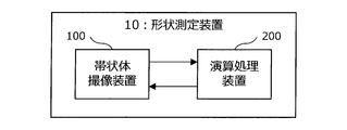
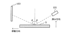
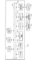
- FIG. 1 is an explanatory view schematically showing the overall configuration of the shape measuring apparatus according to the present embodiment.
- the shape measuring device 10 is a device that measures the surface shape of a band-shaped body made of a metal body, and measures the surface shape of the band-shaped body based on the principle of a light lever. As shown in FIG. 1, the shape measuring apparatus 10 according to the present embodiment mainly includes a strip imaging device 100 and an arithmetic processing device 200.
- the band-shaped body that is the measurement object of the shape measuring apparatus 10 according to the present embodiment is not particularly limited as long as the illumination light is reflected on the surface thereof.
- the belt-like body to be measured is, for example, a metal body such as various steel plates including various types of plated steel plates and various alloy steel plates, various non-ferrous metal plates, and the like. .
- the strip imaging device 100 is mainly composed of a linear light source 101, a screen 103, and an area camera 105 as described later.
- the strip-shaped body imaging device 100 uses a linear light source 101 to form a linear shape on the surface of the strip that moves by being transported on a predetermined transport line under the control of the arithmetic processing device 200 described later. Irradiate light. Further, the strip imaging device 100 sequentially captures the reflected light of the linear light on the surface of the strip projected on the screen 103 using the area camera 105 under the control of the arithmetic processing device 200 described later. Thus, the apparatus outputs a plurality of captured images obtained as a result of imaging to the arithmetic processing apparatus 200.
- the transport line for transporting the strip that is the object to be measured is provided with a PLG (Pulse Logic Generator: pulse type speed detector), etc., and the strip is moved x millimeters regularly (for example, by the transport line). 1 pulse PLG signal is output to the arithmetic processing unit 200.
- the strip imaging device 100 uses the area camera 105 to obtain linear light on the surface of the strip that is projected onto the screen 103 each time a control signal output in accordance with the PLG signal is acquired from the arithmetic processing device 200. The reflected light is imaged.
- the detailed configuration of the strip imaging device 100 will be described in detail below.
- the arithmetic processing device 200 controls the irradiation process of the linear light by the linear light source 101 and the imaging process of the reflected light of the linear light by the area camera 105. In addition, the arithmetic processing device 200 performs predetermined image processing, which will be described in detail below, on a plurality of captured images of the reflected light of the linear light imaged by the belt-shaped body imaging device 100, thereby the surface of the belt-shaped body. Calculate the shape. The detailed configuration of the arithmetic processing device 200 will also be described in detail below.
- the shape measuring apparatus 10 measures the surface shape of the moving strip in a higher speed and in real time as the strip imaging device 100 and the arithmetic processing unit 200 function in cooperation with each other.
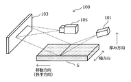
- FIG. 2 is an explanatory diagram schematically illustrating an example of the configuration of the strip-shaped body imaging device included in the shape measuring device according to the present embodiment.
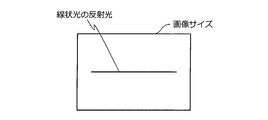
- FIG. 3 is an explanatory diagram schematically illustrating an example of a captured image generated by the strip imaging device according to the present embodiment.
- FIG. 4A, FIG. 4B, FIG. 6 and FIG. 7 are explanatory diagrams for explaining the strip-shaped body imaging device according to the present embodiment.
- FIG. 5 is a graph showing the relationship between the spectral half-width of the linear light and speckle noise, and FIG.
- FIG. 8 is an explanatory diagram showing the relationship between the incident angle of the linear light and the detection state of the surface shape. It is.
- FIG. 9 is a graph showing the relationship between the specular reflection state, the wavelength of the linear light, and the incident angle
- FIG. 10 is an explanatory diagram for explaining the element average length RSm of the roughness curve.
- the band-shaped body imaging device 100 mainly includes a linear light source 101, a screen 103, and an area camera 105 as described later.
- the strip imaging device 100 uses a linear light source 101 on the surface of the moving strip S to spread along the width direction of the strip and is linear light that has a narrow width in the moving direction. Light is irradiated, and the reflected light of the linear light on the surface of the band S is projected onto the screen 103. Then, a plurality of reflected lights of the linear light projected on the screen 103 are imaged using the area camera 105.
- the linear light source 101 may be configured using a known light source such as various lasers or LEDs (Light Emitting Diodes). However, in the present embodiment, among these known light sources, the linear light source 101 is configured using a super luminescent diode (SLD) in order to effectively prevent speckle noise described later.
- a known light source such as various lasers or LEDs (Light Emitting Diodes).
- LEDs Light Emitting Diodes
- SLD super luminescent diode
- the linear light source 101 irradiates the surface of the strip S that moves in a predetermined direction with linear light that is spread along the width direction of the strip S and has a narrow width in the movement direction. .
- a linear light source 101 it is possible to use a combination of the superluminescent diode as described above and various lenses such as a rod lens.
- the light emitted from the linear light source 101 is focused on the surface of the band S by a lens such as a rod lens, and forms a fan-shaped surface. Can be spread.
- linear light that is, linear light
- a lens other than a rod lens such as a cylindrical lens or a Powell lens
- a lens other than a rod lens can be used as long as it can expand the output light in a fan shape while collecting the emitted light. It is.
- the screen 103 is provided at a position facing the linear light source 101, and the reflected light of the linear light reflected by the surface of the strip S is projected.
- the horizontal width of the screen 103 is such that the reflected light corresponding to the entire width of the strip S can be projected according to the spread angle of the linear light and the projection distance to the screen.
- the height of the screen 103 is determined when the projected position of the reflected light changes depending on the shape of the band S, the vibration generated when the band S moves, the change in the thickness of the band S, or the like. Even so, the height is such that the reflected light exists on the projection surface of the screen 103.
- the area camera 105 is provided at a position facing the screen 103 as schematically shown in FIG.
- the area camera 105 is equipped with a lens having a predetermined focal length and an image sensor such as a CCD (Charge Coupled Device) or a CMOS (Complementary Metal Oxide Semiconductor).
- the area camera 105 captures the reflected light of the linear light from the surface of the strip S projected on the projection surface of the screen 103 every time the strip S moves by a predetermined distance, and generates a captured image.
- the angle of view of the area camera 105 is adjusted in advance with reference to past operation data so that the reflected light of the linear light projected on the screen 103 is included in the field of view.
- the surface is set to be imaged under the same imaging conditions.
- the area camera 105 outputs the generated captured image to the arithmetic processing device 200.
- the captured image generated by the area camera 105 is one in which the reflected light of the linear light is reflected at any position of the full frame image size, as schematically shown in FIG.
- the area camera 105 is controlled by the arithmetic processing device 200, and a trigger signal for imaging is output from the arithmetic processing device 200 every time the strip S moves by a predetermined distance.
- the area camera 105 sequentially captures the surface of the screen 103 on which the reflected light of the linear light is projected according to the trigger signal output from the arithmetic processing device 200, and generates the plurality of captured images generated by the arithmetic processing device. Output to 200.
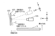
- an XYZ orthogonal coordinate system (right-handed system) fixed to the area camera 105 as shown in FIGS. 4A and 4B is defined.
- the width direction of the imaging field of view of the area camera 105 is the X-axis direction
- the height direction of the imaging field of view of the area camera 105 is the Y-axis direction
- the optical axis direction of the area camera 105 is the Z-axis direction.
- the positional relationship between the screen 103 and the area camera 105 may be as shown by a solid line in FIG. 4A or as shown by a broken line in FIG. 4A. This makes it possible to align the image resolution along the width direction within the field of view of the area camera 105. Further, since it is sufficient that the image resolution along the width direction is uniform, the positional relationship between the screen 103 and the area camera 105 may be a relationship as shown by a solid line in FIG. 4B, and a broken line in FIG.
- FIG. 4B It may be the relationship as shown in. Furthermore, since the image resolution along the width direction is uniform, in FIG. 4B, one of the screen 103 and the area camera 105 is located at a location indicated by a solid line, and the other is located at a location indicated by a broken line. Also good.
- FIG. 2 illustrates the case where only one linear light source 101 is provided.
- a plurality of linear light sources 101 are provided to provide a plurality of linear lights in a strip shape.
- the surface of the body S may be irradiated.
- the plurality of linear lights are irradiated on the surface of the belt-like body S so as to be parallel to each other and at regular intervals along the moving direction. If the width direction of the band S is too large with respect to the field of view of the area camera 105, a plurality of area cameras 105 are provided to divide the reflected light of the linear light into the fields of view of the respective area cameras. Needless to say.
- the linear light source 101 included in the strip imaging device 100 according to the present embodiment irradiates linear light that satisfies various conditions as described in detail below, whereby specifications on the surface of the band S and the projection surface of the screen 103 are obtained. It is possible to prevent the occurrence of noise. As a result, the strip-shaped body imaging apparatus 100 according to the present embodiment can capture the surface shape of the strip S at a higher speed and with higher accuracy without increasing the exposure time during imaging.
- a super luminescent diode that emits light having a central wavelength of 800 nm is used as the linear light source 101 shown in FIG. 2, and the flat surface of the steel plate is irradiated with linear light while changing the spectrum half-value width.
- the reflected light of the linear light projected on the projection plane was imaged.
- the sum of the luminance values of the captured images was calculated along the screen width direction at each position in the screen height direction.
- the spectrum half-value width was set to three kinds of values, 20 nm and 25 nm, and 1 nm corresponding to the spectrum half-width of a general laser beam.
- the total luminance value in the screen width direction smoothly changes when the spectrum half width is 20 nm and when the spectrum half width is 25 nm.
- the spectral half width is 1 nm, the total luminance value in the screen width direction vibrates finely.
- the position coordinate in the screen height direction that gives the maximum total luminance value is common at the position of the coordinate 60 when the spectrum half-value width is 20 nm and 25 nm, and as the distance from the position coordinate that gives the maximum total luminance value increases. The value of the total luminance value decreases smoothly.
- the position coordinate that gives the maximum total luminance value is common at the coordinate 60, but the extremely high total luminance value is obtained even at a position away from the position coordinate that gives the maximum total luminance value.
- the position coordinates shown are present.
- the state of vibration of the total luminance value in the case of the spectral half width of 1 nm shown in FIG. 5 corresponds to speckle noise.
- setting the half-value width of the light source spectrum of linear light to 20 nm or more is useful for preventing the occurrence of speckle noise.
- the upper limit of the spectrum half-value width is a value determined according to the characteristics of the optical system that generates linear light and the value of the line width to be realized.
- a super luminescent diode is used as an incoherent light source capable of emitting a light beam satisfying the spectral half width as described above for the linear light source 101.
- a super luminescent diode as the linear light source 101, not only can speckle noise be suppressed, but the light emitted from a small light emitting point can be used to reduce the line width of the linear light below. It is also possible to narrow down to a desired size as described in detail. As a result, it becomes possible to measure the surface shape of the band-shaped body made of a metal body with higher accuracy.
- a display device such as a projector realizes a plurality of emission points by using a plurality of semiconductor lasers having a wide spectrum half width and different emission wavelengths. In some cases, light of different wavelengths is superimposed on each other.
- the line width of the linear light generated from the laser light cannot be reduced, and the surface shape of the belt-shaped body made of a metal body as noted in this embodiment is increased. It cannot be applied to applications that measure accurately.
- the upper limit value of the wavelength of the linear light emitted from the linear light source 101 is defined by the characteristics of the image sensor mounted on the area camera 105 used in the strip imaging device 100.
- image sensors such as CCD and CMOS are formed using a semiconductor material such as Si or InGaAs, but these semiconductor materials cannot detect light having a wavelength exceeding 1700 nm. Therefore, the upper limit value of the wavelength of the linear light emitted from the linear light source 101 according to the present embodiment is 1700 nm.
- the incident angle of linear light, the lower limit of the wavelength of linear light, and the line width on the surface of the strip will be described.
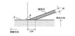
- the angle ⁇ formed by the optical axis of the linear light source 101 and the surface normal direction of the band S is defined as the incident angle ⁇ of the linear light.
- the linear light irradiated from the linear light source 101 shall have a certain finite line width W, as typically shown in FIG. At this time, it is assumed that the linear light having such a line width is incident on the surface of the strip S at an incident angle ⁇ , so that the line width of the linear light is LW on the surface of the strip S.
- the shape measuring apparatus 10 measures the surface shape of the belt-like body based on the principle of the light lever as mentioned above. For that purpose, the linear light irradiated on the surface of the strip must be reflected on the surface of the strip and projected onto the screen. Therefore, in the strip-shaped body imaging device 100 according to the present embodiment, linear light is incident so that the surface of the metal body that often does not have specularity can be regarded as a mirror surface. It is important to control the corners and the wavelength of the linear light.
- ⁇ Standard deviation of irregularities on the surface of the measurement object [ ⁇ m]
- ⁇ Incident angle [degree]
- ⁇ wavelength of light used for measurement [ ⁇ m] It is.
- the parameter g represented by the above equation 1 is g> 1, it is known that the diffuse reflection component increases rapidly. Therefore, in the strip imaging apparatus 100 according to the present embodiment, the parameter g is It is important to be 1 or less.
- the standard deviation ⁇ of fine irregularities on the surface of the measurement object to be detected which is noticed in the shape measuring apparatus 10 according to the present embodiment, is about 0.5 ⁇ m at the maximum, and therefore the strip-shaped body imaging apparatus 100 according to the present embodiment.
- the incident angle ⁇ and the wavelength ⁇ of the linear light must satisfy the following Expression 3. Therefore, in the belt-shaped body imaging device 100 according to the present embodiment, the incident angle ⁇ of the linear light and the wavelength ⁇ of the linear light are arranged so as to satisfy the following Expression 3 regarding the specularity of the belt-shaped body. .
- the above equation 3 is graphed as shown in FIG.
- the wavelength for which the parameter g ⁇ 1 is guaranteed is about 200 nm from the above equation 3 and FIG.
- the superluminescent diode used as the linear light source 101 according to the present embodiment often has an emission wavelength ⁇ of 800 nm or more. Therefore, by using a superluminescent diode and setting the incident angle ⁇ to 88 degrees, the parameter g ⁇ 1 is guaranteed, as is apparent from FIG.
- the magnitude of the incident angle ⁇ that guarantees the parameter g ⁇ 1 is about 74 degrees from the above equation 3 and FIG. Therefore, in the strip imaging device 100 according to the present embodiment, it is preferable that the lower limit of the incident angle is 74 degrees.
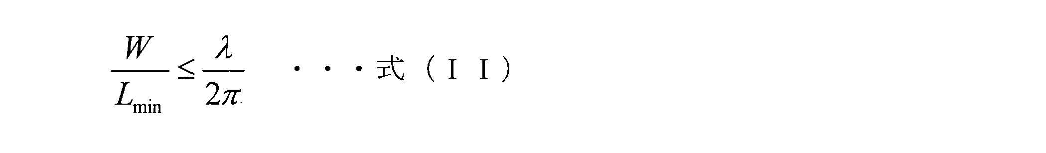
- the following formula 5 ′ can be obtained by modifying the above formula 5, and the lower limit value of the incident angle ⁇ is defined based on the formula 5 ′.
- the upper limit value of the incident angle ⁇ is defined as the following formula 3 ′. Therefore, from the following formulas 3 ′ and 5 ′, the line width W of the linear light along the longitudinal direction of the belt-like body is the minimum value L min of the size along the longitudinal direction of the surface shape to be measured, and the linear shape It is preferably controlled so as to satisfy the following Expression 7 from the wavelength ⁇ of light.
- the incident angle ⁇ of the linear light and the wavelength ⁇ of the linear light satisfy the above formula 3 regarding the specularity of the strip.
- the line width W of the linear light along the longitudinal direction of the belt-like body is the minimum value L min of the size along the longitudinal direction of the surface shape to be measured. It is preferable that the wavelength of the linear light is controlled so as to satisfy the above formula 7.
- the wavelength of the linear light is preferably 800 nm or more and 1700 nm or less.
- the shaped light source is preferably arranged based on the above expression 3 so that the incident angle ⁇ is in the range of 74 degrees to 88 degrees.
- the incident angle ⁇ of the linear light on the surface of the band S is preferably in the range of 80 degrees to 88 degrees.
- the strip imaging device 100 By using the linear light that satisfies the above conditions, the strip imaging device 100 according to the present embodiment has a height of about several ⁇ m and a large size while preventing generation of speckle noise. It is possible to image an extremely fine change in surface shape with a height of about 2 mm with high accuracy.
- the band-shaped body imaging device 100 can perform high-precision imaging processing while preventing generation of speckle noise. is there.
- the power density of the linear light on the surface of the strip can be set to the following range. This makes it possible to perform more reliable imaging processing.
- the brightness of the reflected light of the linear light is set to a higher value, and in order to realize more reliable imaging processing, the linear light on the surface of the band-shaped body
- the power density is preferably 55 mW / cm 2 or more.
- the power density of the linear light on the surface of the belt-like body is better as long as it does not cause a problem on the surface of the belt-like body S, and the power density of the linear light is increased to increase the speed. Even in a simple production line, it is possible to reliably perform an imaging process.
- the power density of the linear light on the surface of the strip is more preferably 491 mW / cm 2 or more, and still more preferably 982 mW / cm 2 or more.
- the preferable power density of the linear light on the surface of the band S is 491 mW / cm 2 or more is that the test result at the line speed of 180 mpm described above is taken into consideration, and the more preferable power density is 982 mW / cm.
- the reason for setting it to 2 or more is that the line speed may increase to 360 mpm due to a change in the operation state of the line.
- the power density there is no upper limit value for exhibiting the effects of the invention in the present embodiment. If the power density is too high, the linear light on the captured image looks thick and the measurement accuracy decreases, but it is easy to obtain appropriate imaging brightness by shortening the exposure time.
- the linear light source 101 included in the strip imaging device 100 according to the present embodiment has been described in detail above with reference to FIGS.
- the strip-shaped body imaging device 100 can obtain linear light that does not include speckle noise, and can perform more reliable imaging processing.
- a screen 103 having a projection surface as described below a clearer captured image can be obtained and measurement with higher accuracy can be performed.
- the surface roughness of the projection surface of the screen 103 is evaluated using the element average length RSm of the roughness curve defined by JIS B0601: 2001 (a standard corresponding to ISO 4287: 1997). I decided to.
- the element average length RSm of the roughness curve defined in JIS B0601: 2001 is the length of the contour curve (roughness curve) element at the reference length Lr of the roughness curve as schematically shown in FIG. It represents the average of the length. Therefore, the element average length RSm of the roughness curve is a value represented by the following expression 11 when there are N contour elements in the reference length Lr.
- Expression 11 below, Xsi is the length of the i-th contour element.
- the minimum height and the minimum length are defined for the peaks (valleys) constituting the contour element. That is, if the height of the mountain (depth of the valley) is 10% or less of the maximum height or the length of the element is 1% or less of the length of the calculation interval, it is regarded as noise, and the valleys that follow ( Handle as part of the mountain.
- the surface unevenness of the projection surface of the screen 103 was observed using a known roughness meter, and the roughness curve of the projection surface of the screen was obtained.
- the element average length RSm of the roughness curve relating to the projection surface of the screen 103 according to the present embodiment is 10 times or more the wavelength of the linear light, and the height direction of the screen on the screen 103 It is preferable that it is 1/10 or less of the line width of the reflected light of the linear light along.
- the element average length Rsm of the roughness curve When the element average length Rsm of the roughness curve is less than 10 times the wavelength of the linear light, the ratio of the regular reflection of the linear light on the projection surface of the screen 103 increases, and the area camera 105 The amount of light received at the may decrease. Further, when the element average length Rsm of the roughness curve is more than 1/10 of the line width of the reflected light of the linear light along the height direction of the screen on the screen 103, the projection surface of the screen 103 The surface roughness of the film becomes too rough, and the tendency of unevenness due to the surface roughness of the screen to occur in the reflected light image of the linear light becomes strong.
- the screen 103 having the surface roughness as described above can be used more suitably.
- a screen 103 is not particularly limited.
- a screen having a metal oxide such as Al 2 O 3 formed on the surface can be used.
- the band-shaped body imaging device 100 according to each embodiment of the present invention has been described in detail above with reference to FIGS.
- the band-shaped body imaging device 100 according to the present embodiment has an arbitrary transfer line in which the band-shaped body S according to the present embodiment is transported within a range in which the imaging process is not physically hindered. It is possible to install at a position.
- the band-shaped body imaging device 100 according to the present embodiment has a portion where the band-shaped body S is positioned on the surface of a roll having a predetermined curvature (in other words, the band-shaped body S is wound around a roll having a predetermined curvature. In such a case, the linear light as described above is applied to the surface of the belt-like body located on the surface of the roll having a predetermined curvature.
- FIG. 11 is a block diagram illustrating an example of a configuration of an arithmetic processing device included in the shape measuring apparatus according to the present embodiment.
- the arithmetic processing device 200 mainly includes an imaging control unit 201, a data acquisition unit 203, an image processing unit 205, a display control unit 207, and a storage unit 209. Prepare for.
- the imaging control unit 201 is realized by, for example, a CPU (Central Processing Unit), a ROM (Read Only Memory), a RAM (Random Access Memory), a communication device, and the like.
- the imaging control unit 201 performs overall control of the imaging process of the reflected light of the linear light by the strip imaging device 100 according to the present embodiment.
- the imaging control unit 201 sends a control signal for starting irradiation of the linear light source 101 to the strip imaging device 100 when imaging of reflected light of linear light is started.
- the imaging control unit 201 periodically transmits a PLG signal from a drive mechanism or the like that controls the transport of the strip S. Each time (for example, a PLG signal output every time the rigid body S moves 1 mm, etc.) is acquired, a trigger signal for starting imaging is sent to the area camera 105.
- the data acquisition unit 203 is realized by, for example, a CPU, a ROM, a RAM, a communication device, and the like.
- the data acquisition unit 203 acquires captured image data output from the strip imaging device 100.
- the data acquisition unit 203 outputs the acquired captured image data to the image processing unit 205 described later.
- the image processing unit 205 is realized by, for example, a CPU, a ROM, a RAM, a communication device, and the like.
- the image processing unit 205 acquires the captured image data generated by the area camera 105, performs image processing described below on the captured image data, and calculates the surface shape of the band S.
- the image processing unit 205 transmits information about the obtained calculation result to the display control unit 207 and the storage unit 209 or is provided outside the shape measuring apparatus 10. Transmitted to various devices.
- the image processing unit 205 will be described in detail later.
- the display control unit 207 is realized by, for example, a CPU, a ROM, a RAM, an output device, a communication device, and the like.
- the display control unit 207 displays the measurement result of the band S transmitted from the image processing unit 205 on an output device such as a display provided in the arithmetic processing device 200, an output device provided outside the arithmetic processing device 200, or the like. Display control is performed. Thereby, the user of the shape measuring apparatus 10 can grasp the measurement result regarding the surface shape of the strip S on the spot.
- the storage unit 209 is an example of a storage device included in the arithmetic processing device 200, and is realized by, for example, a ROM, a RAM, a storage device, or the like.
- the storage unit 209 includes information indicating the optical positional relationship between the linear light source 101 and the area camera 105 included in the belt-shaped body imaging device 100, and a host computer (for example, a transport line) provided outside the shape measuring device 10. Also, information related to design parameters of the shape measuring apparatus 10 such as information transmitted from a management computer or the like that generally manages the information is stored.
- the storage unit 209 stores various parameters that need to be stored when the arithmetic processing apparatus 200 according to the present embodiment performs some processing, and the progress of the processing (for example, the measurement result transmitted from the image processing unit 205). Various data, databases, programs, etc. stored in advance are recorded as appropriate.
- the storage unit 209 can be freely read / written by the imaging control unit 201, the data acquisition unit 203, the image processing unit 205, the display control unit 207, and the host computer.
- FIG. 12 is a block diagram illustrating an example of the configuration of the image processing unit 205 included in the arithmetic processing apparatus according to the present embodiment.
- FIG. 13 is an explanatory diagram schematically showing the relationship between the surface state of the belt-like body and the captured image
- FIG. 14 shows the inclination of the surface of the belt-like body and the amount of displacement of reflected light on the projection surface of the screen. It is explanatory drawing which showed the relationship typically.
- FIG. 15 is an explanatory diagram for explaining the height calculation process performed by the image processing unit according to the present embodiment.
- the image processing unit 205 calculates information on the surface shape of the band S by using the captured image generated by the band imaging device 100 and performing image processing on the captured image. . As illustrated in FIG. 12, the image processing unit 205 includes an inclination angle calculation unit 221, a height calculation unit 223, and a result output unit 225.
- the tilt angle calculation unit 221 is realized by, for example, a CPU, a ROM, a RAM, and the like.
- the inclination angle calculation unit 221 calculates the inclination angle ⁇ of the surface of the band S as information on the surface shape of the band S using the captured image generated by the band imaging device 100.
- the calculation processing of the surface inclination angle ⁇ performed by the inclination angle calculation unit 221 will be described in detail.
- the inclination angle calculation unit 221 calculates the inclination angle ⁇ of the surface of the strip S based on the degree of bending of the reflected image of the linear light in the captured image.
- the reflected image of the linear light in the captured image is The line is almost straight along the width direction of the screen.
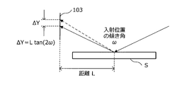
- the surface of the strip S is lowered in the moving direction at the portion irradiated with the linear light (the region surrounded by the broken line in the figure).
- the reflected image of the linear light reflected by the inclined surface is from the position of the reflected image of the flat portion (hereinafter also referred to as “reference position”) in the height direction of the screen. Displaces downward.
- reference position the position of the reflected image of the flat portion
- the captured image includes a straight line portion that is substantially parallel to the width direction of the screen and a downwardly convex portion.
- the surface of the strip S rises in the moving direction at the portion irradiated with the linear light (the region surrounded by the broken line in the figure).
- the reflection image of the linear light reflected by the inclined surface is displaced upward in the height direction of the screen from the position of the reflection image of the flat portion.
- the captured image includes a linear portion that is substantially parallel to the width direction of the screen and an upwardly convex portion.
- the displacement amount of the reflected image from the reference position as schematically shown in the state B and the state C in FIG. 13 is proportional to the magnitude of the inclination angle ⁇ of the surface of the band S. Therefore, the inclination angle calculation unit 221 first determines the position where the luminance distribution in the height direction of the screen 103 (hereinafter also referred to as “Y direction”) is maximum in the captured image by the centroid calculation using the luminance value. Specify the center of the line width of the reflected image. In addition, the inclination angle calculation unit 221 identifies a change in the center position of the line width of the reflected image along the width direction of the screen 103 (hereinafter also referred to as “X direction”) in the captured image. .
- the inclination angle calculation unit 221 makes a difference (that is, from the reference position) with respect to the reference position (that is, the Y coordinate in the linear portion substantially parallel to the width direction of the screen) in each X coordinate in the captured image. Displacement amount ⁇ Y) can be specified.
- the displacement of the reflected image in the captured image is caused by a change in the surface shape larger than the line width LW of the linear light, and the belt-like body S in which the change in the surface shape larger than the line width LW of the linear light occurs.
- the linear light reflected on the surface of the screen moves up and down on the projection surface of the screen 103 in accordance with the direction and angle of inclination of the portion.
- ⁇ Y L ⁇ It is given by tan2 ⁇ .
- L is a horizontal distance from the incident point of the linear light to the band S to the screen 103.
- the inclination angle calculation unit 221 is displaced from the reference position obtained by analyzing the captured image.
- the tilt angle ⁇ can be calculated using the amount ⁇ Y.
- the inclination angle calculation unit 221 can obtain the distribution of the inclination of the surface of the band S in the region irradiated with linear light by performing the processing as described above.
- the data group of the slope values obtained in this way becomes inspection information used when inspecting the shape of the strip S (more specifically, the surface shape).
- the inspection information can also be imaged by replacing the value of the slope included in the inspection information with the level of the luminance value or the density. It is also possible to perform shape inspection based on the tilt image by collecting and generating the data regarding the generated tilt angle between the plurality of captured images and forming the tilt image.
- the inclination angle calculation unit 221 can also inspect the shape of the surface of the strip S by comparing the calculated inclination angle with a predetermined threshold value. That is, by performing a known statistical process or the like based on past operation data or the like, a threshold value of the surface inclination angle when an abnormal portion exists on the surface of the band S is specified in advance, and the storage unit 209 And so on. In addition, the inclination angle calculation unit 221 checks whether or not there is an abnormal portion on the surface of the band S of interest by specifying the magnitude relationship between the calculated inclination angle value and the threshold value. It becomes possible.
- the luminance change caused by speckle noise is not superimposed on the captured image generated by the strip imaging device 100 according to the present embodiment
- the luminance change of the reflected image in the captured image is This is considered to be caused by either a shape change existing on the surface or a dirt adhering to the surface of the band S. Therefore, the inclination angle calculation unit 221 comprehensively considers the information related to the inclination angle specified as described above and the change in the luminance value in the captured image, thereby changing the surface shape and harmless dirt. , Can be distinguished with high accuracy.
- the tilt angle calculation unit 221 outputs data regarding the tilt angle of the surface of the band S generated as described above to the height calculation unit 223.
- the inclination angle calculation unit 221 may output the data itself regarding the generated inclination angle of the surface of the band S, the inspection result of the surface of the band S, and the like to the result output unit 225.
- the height calculation unit 223 is realized by, for example, a CPU, a ROM, a RAM, and the like.
- the height calculation unit 223 uses the inclination angle of the surface of the band S calculated by the inclination angle calculation unit 221, and as the information regarding the surface shape of the band S, the height of the surface of the band S of interest. Is calculated.
- the height calculation unit 223 uses the inclination angle ⁇ of the surface of the band S calculated by the inclination angle calculation unit 221, and the tangent tan ⁇ of the inclination angle as shown in FIG.
- the height of the surface of the strip S is calculated.
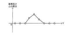
- the height calculation unit 223 performs the integration process as described above on all elements of the data related to the inclination angle of the surface obtained from each captured image, so that the surface of the entire surface of the strip S is obtained.
- a data group (in other words, map data related to the height of the surface) can be obtained.
- the data group relating to the height of the surface obtained in this way becomes inspection information used when inspecting the shape of the strip S (more specifically, the surface shape).
- the information for inspection can be imaged by replacing the value related to the height of the surface included in the information for inspection with the level of the luminance value or the density.
- the height calculation unit 223 can also perform shape inspection based on the height image by imaging the generated map data regarding the height of the surface into a height image.
- the height calculation unit 223 outputs data related to the height of the surface of the band S generated as described above to the result output unit 225.
- the result output unit 225 is realized by, for example, a CPU, a ROM, a RAM, an output device, and the like.
- the result output unit 225 outputs various types of information regarding the surface shape of the strip S generated by the inclination angle calculation unit 221 and the height calculation unit 223 to the display control unit 207. Thereby, various information regarding the measurement result of the surface shape of the strip S is output to a display unit (not shown) such as a display.
- the result output unit 225 may output the obtained calculation result of the surface shape to an external device such as a process computer for manufacturing management, and by using the obtained shape calculation result, various results relating to the product can be output.
- a form may be created.
- the result output unit 225 may store the information related to the surface shape of the band S in association with the time information related to the date and time when the information is calculated, and store the information in the storage unit 209 as history information.
- each component described above may be configured using a general-purpose member or circuit, or may be configured by hardware specialized for the function of each component.
- the CPU or the like may perform all functions of each component. Therefore, it is possible to appropriately change the configuration to be used according to the technical level at the time of carrying out the present embodiment.
- a computer program for realizing each function of the arithmetic processing apparatus according to the present embodiment as described above can be produced and mounted on a personal computer or the like.
- a computer-readable recording medium storing such a computer program can be provided.
- the recording medium is, for example, a magnetic disk, an optical disk, a magneto-optical disk, a flash memory, or the like.
- the above computer program may be distributed via a network, for example, without using a recording medium.
- the surface shape of the belt-like body S is more accurately obtained by using the light lever principle that uses linear light that satisfies a specific condition. It becomes possible to measure. Further, in the shape measuring apparatus 10 according to the present embodiment, the linear light that satisfies a specific condition is condensed on the surface of the band S so as to satisfy a predetermined condition. It becomes possible to reduce the reading height of data, and to further increase the processing speed. In addition, since the shape measuring apparatus 10 according to the present embodiment uses linear light that prevents the occurrence of speckle noise, the change in surface inclination calculated based on the captured image and the luminance value in the captured image Can be detected independently of each other.
- FIG. 16 is a flowchart showing an example of the flow of the shape inspection method according to the present embodiment.
- the linear light source 101 of the strip imaging device 100 of the shape measuring apparatus 10 is linear light as described above with respect to the surface of the strip S under the control of the imaging control unit 201 of the arithmetic processing device 200. Is irradiated so as to satisfy a predetermined condition (step S101). Then, the area camera 105 of the strip imaging device 100 captures the reflected light of the linear light on the projection surface of the screen 103 (step S103), and uses the generated captured image data as the arithmetic processing device 200. Output to.
- the data acquisition unit 203 of the arithmetic processing device 200 acquires the captured image data output from the strip imaging device 100, the data acquisition unit 203 outputs the acquired measurement data to the inclination angle calculation unit 221 of the image processing unit 205.
- the tilt angle calculation unit 221 uses the captured image generated by the strip imaging device 100 to calculate data related to the tilt angle of the surface of the strip S of interest (ie, the tilt angle of the irradiation area of the linear light). (Step S105). Thereafter, the inclination angle calculation unit 221 outputs data regarding the calculated inclination angle to the height calculation unit 223.
- the height calculation unit 223 uses the inclination angle stored in the data related to the inclination angle output from the inclination angle calculation unit 221, and integrates the tangent of the inclination angle to thereby increase the height of the surface of the band S. Is calculated (step S107). The height calculation unit 223 outputs data regarding the height of the surface of the obtained band S to the result output unit 225.
- the result output unit 225 when various types of information regarding the surface shape of the strip S are input, outputs the obtained information to the user and various devices provided outside (step S109). Thereby, the user can grasp various information related to the shape of the band S.
- FIG. 17 is a block diagram for explaining a hardware configuration of the arithmetic processing device 200 according to the embodiment of the present invention.
- the arithmetic processing apparatus 200 mainly includes a CPU 901, a ROM 903, and a RAM 905.
- the arithmetic processing device 200 further includes a bus 907, an input device 909, an output device 911, a storage device 913, a drive 915, a connection port 917, and a communication device 919.
- the CPU 901 functions as a central processing device and control device, and controls all or a part of the operation in the arithmetic processing device 200 according to various programs recorded in the ROM 903, the RAM 905, the storage device 913, or the removable recording medium 921. To do.
- the ROM 903 stores programs used by the CPU 901, calculation parameters, and the like.
- the RAM 905 primarily stores programs used by the CPU 901, parameters that change as appropriate during execution of the programs, and the like. These are connected to each other by a bus 907 constituted by an internal bus such as a CPU bus.
- the bus 907 is connected to an external bus such as a PCI (Peripheral Component Interconnect / Interface) bus via a bridge.
- PCI Peripheral Component Interconnect / Interface
- the input device 909 is an operation means operated by the user such as a mouse, a keyboard, a touch panel, a button, a switch, and a lever.
- the input device 909 may be, for example, remote control means (so-called remote control) using infrared rays or other radio waves, or may be an external connection device 923 such as a PDA corresponding to the operation of the arithmetic processing device 200. May be.
- the input device 909 includes, for example, an input control circuit that generates an input signal based on information input by a user using the operation unit and outputs the input signal to the CPU 901. By operating the input device 909, the user can input various data or instruct processing operations to the arithmetic processing device 200.
- the output device 911 is configured by a device that can notify the user of the acquired information visually or audibly.
- Such devices include display devices such as CRT display devices, liquid crystal display devices, plasma display devices, EL display devices and lamps, audio output devices such as speakers and headphones, printer devices, mobile phones, and facsimiles.
- the output device 911 outputs results obtained by various processes performed by the arithmetic processing device 200, for example. Specifically, the display device displays the results obtained by various processes performed by the arithmetic processing device 200 as text or images.
- the audio output device converts an audio signal composed of reproduced audio data, acoustic data, and the like into an analog signal and outputs the analog signal.
- the storage device 913 is a data storage device configured as an example of a storage unit of the arithmetic processing device 200.
- the storage device 913 includes, for example, a magnetic storage device such as an HDD (Hard Disk Drive), a semiconductor storage device, an optical storage device, or a magneto-optical storage device.
- the storage device 913 stores programs executed by the CPU 901, various data, various data acquired from the outside, and the like.
- the drive 915 is a recording medium reader / writer, and is built in or externally attached to the arithmetic processing unit 200.
- the drive 915 reads information recorded on a removable recording medium 921 such as a mounted magnetic disk, optical disk, magneto-optical disk, or semiconductor memory, and outputs the information to the RAM 905.
- the drive 915 can also write a record on a removable recording medium 921 such as a magnetic disk, an optical disk, a magneto-optical disk, or a semiconductor memory.
- the removable recording medium 921 is, for example, a CD medium, a DVD medium, a Blu-ray (registered trademark) medium, or the like.
- the removable recording medium 921 may be a compact flash (registered trademark) (CompactFlash: CF), a flash memory, an SD memory card (Secure Digital memory card), or the like. Further, the removable recording medium 921 may be, for example, an IC card (Integrated Circuit card) on which a non-contact IC chip is mounted, an electronic device, or the like.
- connection port 917 is a port for directly connecting a device to the arithmetic processing device 200.
- Examples of the connection port 917 include a USB (Universal Serial Bus) port, an IEEE1394 port, a SCSI (Small Computer System Interface) port, and an RS-232C port.
- the communication device 919 is a communication interface configured by a communication device for connecting to the communication network 925, for example.
- the communication device 919 is, for example, a communication card for a wired or wireless LAN (Local Area Network), Bluetooth (registered trademark), or WUSB (Wireless USB).
- the communication device 919 may be a router for optical communication, a router for ADSL (Asymmetric Digital Subscriber Line), or a modem for various communication.
- the communication device 919 can transmit and receive signals and the like according to a predetermined protocol such as TCP / IP, for example, with the Internet and other communication devices.
- the communication network 925 connected to the communication device 919 is configured by a wired or wireless network, for example, the Internet, a home LAN, an in-house LAN, infrared communication, radio wave communication, satellite communication, or the like. May be.
- each component described above may be configured using a general-purpose member, or may be configured by hardware specialized for the function of each component. Therefore, it is possible to change the hardware configuration to be used as appropriate according to the technical level at the time of carrying out this embodiment.
- the shape measuring apparatus and the shape measuring method according to the present invention will be specifically described with reference to examples.
- the Example shown below is an example to the last of the shape measuring apparatus and shape measuring method which concern on this invention, Comprising: The shape measuring apparatus and shape measuring method which concern on this invention are not limited to the following example.
- the surface of a steel plate known to be flat was imaged using a strip imaging device 100 as shown in FIG.
- the linear light source 101 using a superluminescent diode capable of emitting light having a wavelength of 800 nm with a spectral half width of 30 nm, the linear light is directed from the position 300 mm away from the steel plate surface toward the steel plate surface. Irradiation was conducted while condensing so that the incident angle ⁇ was 83 degrees.
- the wavelength ⁇ and the incident angle ⁇ of the linear light as described above satisfy the relationship represented by the above formula (3).
- the line width LW of the linear light on the steel sheet surface was 2 mm, and the power density of the linear light on the steel sheet surface was 55 mW / cm 2 .
- the screen 103 using the Al 2 O 3 plate which is the formation of the Al 2 O 3 film on the surface.
- the element average length RSm of the roughness curve on the projection surface is 0.01 mm, and the value of the RSm satisfies the condition described above.
- the area camera 105 an area camera equipped with a general image sensor was used.
- the separation distance between screen 103 and area camera 105 (distance L in FIG. 14) was 350 mm.
- the imaging resolution on the projection surface of the screen 103 is 0.2 mm / pixel.
- imaging was performed in the same manner using a laser light source having a wavelength of 810 nm with a spectral half-width of 1 nm.
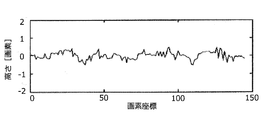
- the center position of the line width of the reflected image was calculated by calculating the center of gravity using the luminance value, and the transition of the center position was specified along the width direction of the screen.
- FIGS. 18A and 18B show the obtained results when a super luminescent diode is used as the linear light source 101
- FIG. 18B shows the result when a laser light source is used as the linear light source 101.
- the unit of the vertical axis and the horizontal axis is a pixel, and one pixel corresponds to 0.2 mm.
- the transition of the center position of the line width of the reflected image should ideally be almost flat.
- the laser light source when used, speckle noise is generated and the center position of the line width of the reflected image fluctuates violently. It can be seen that when the nescent diode is used, the fluctuation of the center position of the line width of the reflected image is well suppressed.
- SYMBOLS 10 Shape measuring apparatus 100 Strip body imaging device 101 Linear light source 103 Screen 105 Area camera 200 Arithmetic processing device 201 Imaging control part 203 Data acquisition part 205 Image processing part 207 Display control part 209 Storage part 221 Inclination angle calculation part 223 Height calculation Part 225 Result output part
Landscapes
- Physics & Mathematics (AREA)
- General Physics & Mathematics (AREA)
- Engineering & Computer Science (AREA)
- Health & Medical Sciences (AREA)
- Life Sciences & Earth Sciences (AREA)
- Chemical & Material Sciences (AREA)
- Analytical Chemistry (AREA)
- Biochemistry (AREA)
- General Health & Medical Sciences (AREA)
- Immunology (AREA)
- Pathology (AREA)
- Textile Engineering (AREA)
- Mathematical Physics (AREA)
- Theoretical Computer Science (AREA)
- Data Mining & Analysis (AREA)
- Algebra (AREA)
- Mathematical Optimization (AREA)
- Mathematical Analysis (AREA)
- Pure & Applied Mathematics (AREA)
- Databases & Information Systems (AREA)
- Software Systems (AREA)
- General Engineering & Computer Science (AREA)
- Computational Mathematics (AREA)
- Length Measuring Devices By Optical Means (AREA)
Abstract
Description
前記帯状体の表面に対して、前記帯状体の幅方向に広がる線状光を照射する、スーパールミネッセントダイオード(SuperLuminescent Diode)からなる線状光源と、前記帯状体の表面での前記線状光の反射光が投影されるスクリーンと、前記スクリーンに投影された前記線状光の反射光を撮像するエリアカメラと、前記エリアカメラにより撮像された前記線状光の反射光の撮像画像を用いて、前記帯状体の表面形状を算出する演算処理装置と、を備え、前記線状光源は、スペクトル半値幅が20nm以上であり、かつ、前記線状光源の光軸と前記帯状体の表面法線方向とのなす角θと、前記線状光の波長λとが、前記帯状体の鏡面性に関する以下の式(I)を満足するように配置されている、形状測定装置が提供される。


まず、図1を参照しながら、本発明の実施形態に係る形状測定装置の全体構成について説明する。図1は、本実施形態に係る形状測定装置の全体構成を模式的に示した説明図である。
次に、図2~図10を参照しながら、本実施形態に係る形状測定装置10が備える帯状体撮像装置100の構成について、詳細に説明する。
図2は、本実施形態に係る形状測定装置が有する帯状体撮像装置の構成の一例を模式的に示した説明図である。図3は、本実施形態に係る帯状体撮像装置により生成される撮像画像の一例を模式的に示した説明図である。図4A、図4B、図6及び図7は、本実施形態に係る帯状体撮像装置について説明するための説明図である。図5は、線状光のスペクトル半値幅とスペックルノイズとの関係を示したグラフ図であり、図8は、線状光の入射角と表面形状の検出状況との関係を示した説明図である。図9は、鏡面反射状態と線状光の波長及び入射角との関係を示したグラフ図であり、図10は、粗さ曲線の要素平均長さRSmについて説明するための説明図である。
帯状体撮像装置100は、主に、後述するような、線状光源101、スクリーン103及びエリアカメラ105から構成される。
帯状体撮像装置100は、移動する帯状体Sの表面に対して、線状光源101を用いて、帯状体の幅方向に沿って広がり、かつ、移動方向に狭い幅を有する光である線状光を照射し、帯状体Sの表面での線状光の反射光をスクリーン103に投影させる。そして、スクリーン103に投影された線状光の反射光を、エリアカメラ105を用いて複数撮像する。
続いて、図5~図9を参照しながら、本実施形態に係る帯状体撮像装置100が有する線状光源101について、詳細に説明する。
本実施形態に係る線状光源101は、以下で詳述するような諸条件を満足する線状光を照射することで、帯状体Sの表面上、及び、スクリーン103の投影面上でのスペックルノイズの発生を防止することが可能となる。その結果、本実施形態に係る帯状体撮像装置100は、撮像の際の露光時間を長くすることなく、帯状体Sの表面形状をより高速かつより高精度に撮像することができる。
○スペクトル半値幅の下限について
まず、本実施形態に係る線状光源101から照射される線状光の光源スペクトル(波長と照射光の強度との関係)について着目する。本実施形態に係る線状光源101では、光源としてスーパールミネッセントダイオードを用い、線状光のスペクトルの半値幅(半値全幅)を、20nm以上とする。本実施形態に係る線状光源101では、出射する線状光をスペクトル半値幅が20nm以上とすることで、スペックルノイズの発生を防止することが可能となる。
線状光のスペクトルの半値幅が大きい場合は、光学系の色収差により集光が困難になり、後述する表面での線幅の制約が満たせなくなる。そのため、スペクトル半値幅の上限は、線状光を生成する光学系の特性と、実現すべき線幅の値と、に応じて決まる値となる。
線状光源101から照射される線状光の波長の上限値は、帯状体撮像装置100に用いられるエリアカメラ105に搭載された撮像素子の特性により規定される。一般的に用いられるCCDやCMOS等の撮像素子は、SiやInGaAs等の半導体材料を用いて形成されているが、これらの半導体材料は、波長1700nmを超える光を検出することができない。そのため、本実施形態に係る線状光源101から照射される線状光の波長の上限値は、1700nmとする。
続いて、線状光の入射角、線状光の波長の下限、及び、帯状体の表面での線幅について説明する。
図6に示したように、線状光源101の光軸と帯状体Sの表面法線方向とのなす角θを、線状光の入射角θとする。また、線状光源101から照射される線状光は、図7に模式的に示したように、ある有限の線幅Wを有しているものとする。この際に、かかる線幅の線状光が入射角θで帯状体Sの表面に入射することで、帯状体Sの表面において、線状光の線幅がLWとなっているものとする。
図7に模式的に示したような帯状体Sの表面での線幅LWは、どの程度の微細な表面形状を測定したいかに応じて、設定される。本実施形態に係る形状測定装置10において着目する、検出したい微細な表面形状の大きさ(帯状体Sの表面位置(高さ)での形状の特異部分についての、搬送方向の広がりの程度)は、最大でも2mm程度である。そのため、図7に示した帯状体Sの表面での線状光の線幅LWは、最大2mmとする。
本実施形態に係る形状測定装置10は、先だって言及したように、光てこの原理に基づいて、帯状体の表面形状を測定する。そのためには、帯状体の表面に照射された線状光が帯状体の表面で反射して、スクリーン上に投影されなければならない。従って、本実施形態に係る帯状体撮像装置100では、元来、鏡面性を有していないことが多い金属体の表面があたかも鏡面とみなすことができる状態となるように、線状光の入射角と、線状光の波長と、を制御することが重要となる。

σ:測定対象物の表面における凹凸の標準偏差[μm]
θ:入射角[度]
λ:測定に用いる光の波長[μm]
である。

入射角θの上限値である88度において、パラメータg≦1が保証される波長は、上記式3及び図9から、約200nmである。本実施形態に係る線状光源101として用いられるスーパールミネッセントダイオードは、発光波長λが800nm以上であることが多い。そのため、スーパールミネッセントダイオードを用いて、入射角θを88度とすることで、図9から明らかなように、パラメータg≦1が保証される。一方、線状光の波長の上限である1700nmにおいて、パラメータg≦1が保証される入射角θの大きさは、上記式3及び図9から、約74度となる。従って、本実施形態に係る帯状体撮像装置100において、入射角の下限を74度とすることが好ましい。


以上のような条件を満足する線状光を用いることで、本実施形態に係る帯状体撮像装置100では、スペックルノイズの発生を防止しつつ、高精度の撮像処理を実施することが可能である。この際、帯状体の表面での線状光のパワー密度を以下のような範囲とすることで、スクリーン103の投影面上において、線状光の反射光の輝度をより高い値とすることができ、より確実な撮像処理を実施することが可能となる。
以上のような条件を満足することで、本実施形態に係る帯状体撮像装置100では、スペックルノイズを含まない線状光を得ることが可能となり、より確実な撮像処理を実施可能である。この際、以下で示すような投影面を有するスクリーン103を利用することで、より鮮明な撮像画像を得ることができ、より高精度な測定を実施することが可能となる。

<演算処理装置200の全体構成について>
続いて、図11を参照しながら、本実施形態に係る演算処理装置200の全体構成について、詳細に説明する。図11は、本実施形態に係る形状測定装置が有する演算処理装置の構成の一例を示したブロック図である。
次に、図12~図15を参照しながら、本実施形態に係る演算処理装置200が有する画像処理部205について、詳細に説明する。
図12は、本実施形態に係る演算処理装置が有する画像処理部205の構成の一例を示したブロック図である。図13は、帯状体の表面状態と撮像画像との関係を模式的に示した説明図であり、図14は、帯状体の表面の傾きとスクリーンの投影面上における反射光の変位量との関係を模式的に示した説明図である。図15は、本実施形態に係る画像処理部で実施される高さ算出処理を説明するための説明図である。
次に、図16を参照しながら、本実施形態に係る形状測定装置10で実施される形状検査方法の流れの一例について、簡単に説明する。図16は、本実施形態に係る形状検査方法の流れの一例を示した流れ図である。
次に、図17を参照しながら、本発明の各実施形態に係る演算処理装置200のハードウェア構成について、詳細に説明する。図17は、本発明の実施形態に係る演算処理装置200のハードウェア構成を説明するためのブロック図である。
この際、線状光源101として、波長800nmの光をスペクトル半値幅30nmで出射可能なスーパールミネッセントダイオードを利用し、鋼板表面から300mm離れた位置から鋼板表面に向けて、線状光を、入射角θ=83度となるように集光しつつ照射した。上記のような線状光の波長λ及び入射角θは、上記式(3)で表される関係を満足している。なお、鋼板表面における線状光の線幅LWは、2mmとし、鋼板表面における線状光のパワー密度は、55mW/cm2となるようにした。
100 帯状体撮像装置
101 線状光源
103 スクリーン
105 エリアカメラ
200 演算処理装置
201 撮像制御部
203 データ取得部
205 画像処理部
207 表示制御部
209 記憶部
221 傾き角算出部
223 高さ算出部
225 結果出力部
Claims (20)
- 金属体からなる帯状体の表面形状を測定する形状測定装置であって、
前記帯状体の表面に対して、前記帯状体の幅方向に広がる線状光を照射する、スーパールミネッセントダイオード(SuperLuminescent Diode)からなる線状光源と、
前記帯状体の表面での前記線状光の反射光が投影されるスクリーンと、
前記スクリーンに投影された前記線状光の反射光を撮像するエリアカメラと、
前記エリアカメラにより撮像された前記線状光の反射光の撮像画像を用いて、前記帯状体の表面形状を算出する演算処理装置と、
を備え、
前記線状光源は、
スペクトル半値幅が20nm以上であり、かつ、
前記線状光源の光軸と前記帯状体の表面法線方向とのなす角θと、前記線状光の波長λとが、前記帯状体の鏡面性に関する以下の式(I)を満足するように配置されている、形状測定装置。

- 前記帯状体の表面において、前記帯状体の長手方向に沿った前記線状光の線幅Wは、測定したい前記表面形状の前記長手方向に沿った大きさの最小値をLminとし、前記線状光の波長をλとしたときに、以下の式(II)を満足するように制御される、請求項1に記載の形状測定装置。

- 前記線状光の波長は、800nm以上1700nm以下である、請求項1又は2に記載の形状測定装置。
- 前記線状光源は、前記線状光源の光軸と前記帯状体の表面法線方向とのなす角θが74度以上88度以下の範囲内となるように、前記式(I)に基づき配置される、請求項1~3の何れか1項に記載の形状測定装置。
- 前記帯状体の表面での前記線状光のパワー密度は、55mW/cm2以上である、請求項1~4の何れか1項に記載の形状測定装置。
- 前記スクリーンにおける前記線状光の反射光の投影面は、JIS B0601:2001で規定される粗さ曲線の要素平均長さRSmが、前記線状光の波長の10倍以上であり、かつ、当該スクリーン上での前記スクリーンの高さ方向に沿った前記線状光の反射光の線幅の1/10以下である表面粗さを有する、請求項1~5の何れか1項に記載の形状測定装置。
- 前記線状光は、所定の曲率を有するロールの表面上に位置する前記帯状体の表面に対して照射される、請求項1~6の何れか1項に記載の形状測定装置。
- 前記演算処理装置は、前記撮像画像における前記反射光の基準位置からの変位量から、前記表面形状に関する情報として前記帯状体の表面の傾き角を算出する、請求項1~7の何れか1項に記載の形状測定装置。
- 前記演算処理装置は、算出した前記帯状体の表面の傾き角の正接を前記エリアカメラと前記帯状体の相対的な移動方向に沿って積分することで、前記表面形状に関する情報として前記帯状体の表面の高さを算出する、請求項8に記載の形状測定装置。
- 前記演算処理装置は、算出した前記帯状体の表面の傾き角を所定の閾値と比較することで、前記帯状体の形状を検査する、請求項8又は9に記載の形状測定装置。
- 金属体からなる帯状体の表面形状を測定する形状測定方法であって、
前記帯状体の表面に対して、スーパールミネッセントダイオード(SuperLuminescent Diode)からなる線状光源を用いて、前記帯状体の幅方向に広がる線状光を照射する照射ステップと、
スクリーンに対し、前記帯状体の表面での前記線状光の反射光を投影するステップと、
エリアカメラを用いて、前記スクリーンに投影された前記線状光の反射光を撮像する撮像ステップと、
前記エリアカメラにより撮像された前記線状光の反射光の撮像画像を用いて、前記帯状体の表面形状を算出する算出ステップと、
を含み、
前記線状光源は、
スペクトル半値幅が20nm以上であり、かつ、
前記線状光源の光軸と前記帯状体の表面法線方向とのなす角θと、前記線状光の波長λとが、前記帯状体の鏡面性に関する以下の式(I)を満足するように配置されている、形状測定方法。

- 前記帯状体の表面において、前記帯状体の長手方向に沿った前記線状光の線幅Wは、測定したい前記表面形状の前記長手方向に沿った大きさの最小値をLminとし、前記線状光の波長をλとしたときに、以下の式(II)を満足するように制御される、請求項11に記載の形状測定方法。

- 前記線状光の波長は、800nm以上1700nm以下である、請求項11又は12の何れか1項に記載の形状測定方法。
- 前記線状光源は、前記線状光源の光軸と前記帯状体の表面法線方向とのなす角θが74度以上88度以下の範囲内となるように、前記式(I)に基づき配置される、請求項11~13の何れか1項に記載の形状測定方法。
- 前記帯状体の表面での前記線状光のパワー密度は、55mW/cm2以上である、請求項11~14の何れか1項に記載の形状測定方法。
- 前記スクリーンにおける前記線状光の反射光の投影面は、JIS B0601:2001で規定される粗さ曲線の要素平均長さRSmが、前記線状光の波長の10倍以上であり、かつ、当該スクリーン上での前記スクリーンの高さ方向に沿った前記線状光の反射光の線幅の1/10以下である表面粗さを有する、請求項11~15の何れか1項に記載の形状測定方法。
- 前記線状光は、所定の曲率を有するロールの表面上に位置する前記帯状体の表面に対して照射される、請求項11~16の何れか1項に記載の形状測定方法。
- 前記算出ステップは、前記撮像画像における前記反射光の基準位置からの変位量から、前記表面形状に関する情報として前記帯状体の表面の傾き角を算出する、請求項11~17の何れか1項に記載の形状測定方法。
- 前記算出ステップは、算出した前記帯状体の表面の傾き角の正接を前記エリアカメラと前記帯状体の相対的な移動方向に沿って積分することで、前記表面形状に関する情報として前記帯状体の表面の高さを算出する、請求項18に記載の形状測定方法。
- 算出された前記帯状体の表面の傾き角を所定の閾値と比較して、前記帯状体の形状を検査する検査ステップを更に含む、請求項18又は19に記載の形状測定方法。
Priority Applications (5)
| Application Number | Priority Date | Filing Date | Title |
|---|---|---|---|
| US15/738,499 US10605591B2 (en) | 2016-05-23 | 2017-05-19 | Shape measurement apparatus and shape measurement method |
| EP17802711.6A EP3309508B1 (en) | 2016-05-23 | 2017-05-19 | Shape measurement device and shape measurement method |
| CN201780002621.5A CN107850422A (zh) | 2016-05-23 | 2017-05-19 | 形状测定装置和形状测定方法 |
| KR1020187002605A KR101994051B1 (ko) | 2016-05-23 | 2017-05-19 | 형상 측정 장치 및 형상 측정 방법 |
| JP2017550258A JP6281667B1 (ja) | 2016-05-23 | 2017-05-19 | 形状測定装置及び形状測定方法 |
Applications Claiming Priority (2)
| Application Number | Priority Date | Filing Date | Title |
|---|---|---|---|
| JP2016-102330 | 2016-05-23 | ||
| JP2016102330 | 2016-05-23 |
Publications (1)
| Publication Number | Publication Date |
|---|---|
| WO2017204119A1 true WO2017204119A1 (ja) | 2017-11-30 |
Family
ID=60412803
Family Applications (1)
| Application Number | Title | Priority Date | Filing Date |
|---|---|---|---|
| PCT/JP2017/018897 Ceased WO2017204119A1 (ja) | 2016-05-23 | 2017-05-19 | 形状測定装置及び形状測定方法 |
Country Status (6)
| Country | Link |
|---|---|
| US (1) | US10605591B2 (ja) |
| EP (1) | EP3309508B1 (ja) |
| JP (1) | JP6281667B1 (ja) |
| KR (1) | KR101994051B1 (ja) |
| CN (1) | CN107850422A (ja) |
| WO (1) | WO2017204119A1 (ja) |
Cited By (4)
| Publication number | Priority date | Publication date | Assignee | Title |
|---|---|---|---|---|
| JP2020051874A (ja) * | 2018-09-26 | 2020-04-02 | 日本製鉄株式会社 | 表面測定装置及び表面測定方法 |
| JP2021131320A (ja) * | 2020-02-20 | 2021-09-09 | 有限会社折原製作所 | 強化ガラスの応力測定装置、強化ガラスの応力測定方法 |
| WO2021199299A1 (ja) * | 2020-03-31 | 2021-10-07 | 日本製鉄株式会社 | 表面測定装置及び表面測定方法 |
| JP2021162584A (ja) * | 2020-03-31 | 2021-10-11 | Jfeスチール株式会社 | 表面欠陥検出装置、表面欠陥検出方法、鋼板の製造方法、鋼板の品質管理方法、及び、鋼板の製造設備 |
Families Citing this family (14)
| Publication number | Priority date | Publication date | Assignee | Title |
|---|---|---|---|---|
| WO2018200685A2 (en) | 2017-04-27 | 2018-11-01 | Ecosense Lighting Inc. | Methods and systems for an automated design, fulfillment, deployment and operation platform for lighting installations |
| PL3575741T3 (pl) * | 2018-05-29 | 2025-01-20 | Manroland Goss Web Systems Gmbh | Sposób bezdotykowego pomiaru konturu krawędzi przedmiotu obrabianego |
| CN109238181B (zh) * | 2018-09-29 | 2023-09-26 | 昆明理工大学 | 一种基于多级光杠杆的电梯轨道平整度检测系统及方法 |
| CN109612408B (zh) * | 2018-12-11 | 2021-12-07 | 信利光电股份有限公司 | 半导体激光器发射角度测试方法、装置及可读存储介质 |
| DE102020002357A1 (de) * | 2019-04-19 | 2020-10-22 | Mitutoyo Corporation | Messapparat für eine dreidimensionale geometrie und messverfahren für eine dreidimensionale geometrie |
| JP7207386B2 (ja) * | 2019-10-29 | 2023-01-18 | Jfeスチール株式会社 | 表面欠陥検査方法、表面欠陥検査装置、鋼板の製造方法、鋼板の品質管理方法及び鋼板の製造設備 |
| US11690490B2 (en) | 2020-07-08 | 2023-07-04 | Pixart Imaging Inc. | Auto clean machine and auto clean machine control method |
| JP2022191111A (ja) * | 2021-06-15 | 2022-12-27 | 稔 新村 | 無塗装耐候性鋼橋さびレベルの判定手段 |
| US20250139755A1 (en) * | 2021-09-27 | 2025-05-01 | Toray Industries, Inc. | Unevenness measuring device for sheet-shaped material, and unevenness measuring method for sheet-shaped material |
| CN114544208A (zh) * | 2021-11-04 | 2022-05-27 | 万向一二三股份公司 | 一种超声焊接机稳定性检测装置和方法 |
| CN114166768B (zh) * | 2022-02-14 | 2022-05-20 | 四川大学华西医院 | 不同设备检测同一指标同质化换算方法、装置、电子设备 |
| JP2023148723A (ja) * | 2022-03-30 | 2023-10-13 | リンテック株式会社 | 視野角制御フィルム |
| JP2023178850A (ja) * | 2022-06-06 | 2023-12-18 | キヤノン株式会社 | 画像処理装置、画像処理方法、及びプログラム |
| CN117213411B (zh) * | 2023-11-08 | 2024-01-05 | 天津欧派集成家居有限公司 | 基于机器视觉的装饰板材平整度智能检测装置及检测方法 |
Citations (10)
| Publication number | Priority date | Publication date | Assignee | Title |
|---|---|---|---|---|
| JPS6262205A (ja) * | 1985-09-13 | 1987-03-18 | Toray Ind Inc | 物体の表面凹凸検査方法 |
| JPH08233541A (ja) * | 1995-02-23 | 1996-09-13 | Murata Mfg Co Ltd | シート厚み測定方法 |
| JPH11316111A (ja) * | 1998-04-30 | 1999-11-16 | Asahi Glass Co Ltd | 板状鏡面体の表面形状測定方法および装置 |
| JP2004184397A (ja) * | 2002-10-08 | 2004-07-02 | Nippon Steel Corp | 帯状体の形状不良検査方法およびその装置 |
| WO2007032216A1 (ja) * | 2005-09-14 | 2007-03-22 | Matsushita Electric Industrial Co., Ltd. | 画像形成装置 |
| JP2009111230A (ja) * | 2007-10-31 | 2009-05-21 | Sony Corp | レーザモジュール |
| JP2012078144A (ja) * | 2010-09-30 | 2012-04-19 | Kaneka Corp | 透明体シート状物の表面欠陥検査装置 |
| JP2014153149A (ja) * | 2013-02-07 | 2014-08-25 | Nikon Corp | 形状測定装置、構造物製造システム、形状測定方法、及びプログラム |
| JP2014178323A (ja) * | 2014-04-16 | 2014-09-25 | Dainippon Printing Co Ltd | 線状照明装置 |
| US20160169798A1 (en) * | 2013-08-21 | 2016-06-16 | Fraunhofer-Gesellschaft Zur Foerderung Der Angewandten Forschung E.V. | Device and method for sensing at least one partially specular surface |
Family Cites Families (23)
| Publication number | Priority date | Publication date | Assignee | Title |
|---|---|---|---|---|
| NL279098A (ja) * | 1961-05-31 | |||
| JPH0599639A (ja) | 1991-10-09 | 1993-04-23 | Mitsubishi Rayon Co Ltd | 平面状物の緩やかな凹凸検査装置 |
| JP2002197993A (ja) * | 2000-12-26 | 2002-07-12 | Nippon Electric Glass Co Ltd | カラー陰極線管用ファンネル |
| US7132212B2 (en) * | 2001-06-13 | 2006-11-07 | Fuji Photo Film Co., Ltd. | Presensitized plate |
| US20090130434A1 (en) * | 2006-03-28 | 2009-05-21 | Kyocera Corporation | Surface Coated Tool |
| US20070246158A1 (en) * | 2006-04-21 | 2007-10-25 | 3M Innovative Properties Company | Wiring board, production process thereof and connection method using same |
| JP2010020268A (ja) * | 2008-06-09 | 2010-01-28 | Sony Corp | 光学フィルムおよびその製造方法、防眩性フィルム、光学層付偏光子、ならびに表示装置 |
| KR20100020906A (ko) * | 2008-08-13 | 2010-02-23 | 소니 가부시끼가이샤 | 광학 필름 및 그 제조 방법, 눈부심방지성 필름, 광학층이 부착된 편광자 및 표시 장치 |
| US8520223B2 (en) * | 2009-05-26 | 2013-08-27 | Udo Wolfgang Bucher | Wet paint coating thickness measurement and instrument |
| JP5903999B2 (ja) * | 2011-06-16 | 2016-04-13 | 株式会社リコー | 感光体ドラム、画像形成装置、画像形成方法、及びプロセスカートリッジ |
| TWI423785B (zh) * | 2011-07-26 | 2014-01-21 | 國立交通大學 | 生理訊號蒐集單元及其探頭 |
| US10914037B2 (en) * | 2012-10-09 | 2021-02-09 | Michael Gorden | Yankee dryer profiler and control |
| AU2013352267B2 (en) * | 2012-11-30 | 2017-04-13 | 3M Innovative Properties Company | Transparent note sheet and method for manufacturing the same |
| US9131219B2 (en) | 2012-12-18 | 2015-09-08 | Institut National D'optique | Method and apparatus for triangulation-based 3D optical profilometry |
| US10448584B2 (en) * | 2013-10-07 | 2019-10-22 | Kuraray Co., Ltd. | Medium for plant cultivation, and apparatus and method for plant cultivation including the same |
| JP6100203B2 (ja) * | 2014-05-19 | 2017-03-22 | 日新製鋼株式会社 | 接続部品用材料 |
| CN106250800B (zh) * | 2015-06-05 | 2021-08-27 | Agc株式会社 | 一种保护玻璃以及便携式信息终端 |
| CN208378728U (zh) * | 2015-06-12 | 2019-01-15 | Agc株式会社 | 玻璃板和显示装置 |
| JP6532345B2 (ja) * | 2015-08-05 | 2019-06-19 | キヤノン株式会社 | 画像形成装置 |
| TWM519751U (zh) * | 2015-11-09 | 2016-04-01 | 大立光電股份有限公司 | 塑膠鏡筒、鏡頭模組及電子裝置 |
| JP6648547B2 (ja) * | 2016-02-10 | 2020-02-14 | 富士ゼロックス株式会社 | 静電荷像現像剤、現像剤カートリッジ、プロセスカートリッジ、画像形成装置、及び、画像形成方法 |
| JP6750245B2 (ja) * | 2016-02-19 | 2020-09-02 | 富士ゼロックス株式会社 | 静電荷像現像用トナー、静電荷像現像剤、トナーカートリッジ、プロセスカートリッジ、画像形成装置、及び画像形成方法 |
| DE102016119728A1 (de) * | 2016-10-17 | 2018-04-19 | Inoex Gmbh Lnnovationen Und Ausrüstungen Für Die Extrusionstechnik | Terahertz-Messgerät |
-
2017
- 2017-05-19 EP EP17802711.6A patent/EP3309508B1/en active Active
- 2017-05-19 KR KR1020187002605A patent/KR101994051B1/ko active Active
- 2017-05-19 CN CN201780002621.5A patent/CN107850422A/zh not_active Withdrawn
- 2017-05-19 JP JP2017550258A patent/JP6281667B1/ja active Active
- 2017-05-19 US US15/738,499 patent/US10605591B2/en active Active
- 2017-05-19 WO PCT/JP2017/018897 patent/WO2017204119A1/ja not_active Ceased
Patent Citations (10)
| Publication number | Priority date | Publication date | Assignee | Title |
|---|---|---|---|---|
| JPS6262205A (ja) * | 1985-09-13 | 1987-03-18 | Toray Ind Inc | 物体の表面凹凸検査方法 |
| JPH08233541A (ja) * | 1995-02-23 | 1996-09-13 | Murata Mfg Co Ltd | シート厚み測定方法 |
| JPH11316111A (ja) * | 1998-04-30 | 1999-11-16 | Asahi Glass Co Ltd | 板状鏡面体の表面形状測定方法および装置 |
| JP2004184397A (ja) * | 2002-10-08 | 2004-07-02 | Nippon Steel Corp | 帯状体の形状不良検査方法およびその装置 |
| WO2007032216A1 (ja) * | 2005-09-14 | 2007-03-22 | Matsushita Electric Industrial Co., Ltd. | 画像形成装置 |
| JP2009111230A (ja) * | 2007-10-31 | 2009-05-21 | Sony Corp | レーザモジュール |
| JP2012078144A (ja) * | 2010-09-30 | 2012-04-19 | Kaneka Corp | 透明体シート状物の表面欠陥検査装置 |
| JP2014153149A (ja) * | 2013-02-07 | 2014-08-25 | Nikon Corp | 形状測定装置、構造物製造システム、形状測定方法、及びプログラム |
| US20160169798A1 (en) * | 2013-08-21 | 2016-06-16 | Fraunhofer-Gesellschaft Zur Foerderung Der Angewandten Forschung E.V. | Device and method for sensing at least one partially specular surface |
| JP2014178323A (ja) * | 2014-04-16 | 2014-09-25 | Dainippon Printing Co Ltd | 線状照明装置 |
Non-Patent Citations (1)
| Title |
|---|
| See also references of EP3309508A4 * |
Cited By (9)
| Publication number | Priority date | Publication date | Assignee | Title |
|---|---|---|---|---|
| JP2020051874A (ja) * | 2018-09-26 | 2020-04-02 | 日本製鉄株式会社 | 表面測定装置及び表面測定方法 |
| JP7284562B2 (ja) | 2018-09-26 | 2023-05-31 | 日本製鉄株式会社 | 表面測定装置及び表面測定方法 |
| JP2021131320A (ja) * | 2020-02-20 | 2021-09-09 | 有限会社折原製作所 | 強化ガラスの応力測定装置、強化ガラスの応力測定方法 |
| JP7284512B2 (ja) | 2020-02-20 | 2023-05-31 | 有限会社折原製作所 | 強化ガラスの応力測定装置、強化ガラスの応力測定方法 |
| WO2021199299A1 (ja) * | 2020-03-31 | 2021-10-07 | 日本製鉄株式会社 | 表面測定装置及び表面測定方法 |
| JP2021162584A (ja) * | 2020-03-31 | 2021-10-11 | Jfeスチール株式会社 | 表面欠陥検出装置、表面欠陥検出方法、鋼板の製造方法、鋼板の品質管理方法、及び、鋼板の製造設備 |
| JP7014338B1 (ja) * | 2020-03-31 | 2022-02-01 | 日本製鉄株式会社 | 表面測定装置及び表面測定方法 |
| JP7207443B2 (ja) | 2020-03-31 | 2023-01-18 | Jfeスチール株式会社 | 表面欠陥検出装置、表面欠陥検出方法、鋼板の製造方法、鋼板の品質管理方法、及び、鋼板の製造設備 |
| US12435972B2 (en) | 2020-03-31 | 2025-10-07 | Nippon Steel Corporation | Surface measurement apparatus and surface measurement method |
Also Published As
| Publication number | Publication date |
|---|---|
| KR101994051B1 (ko) | 2019-06-27 |
| JP6281667B1 (ja) | 2018-02-21 |
| EP3309508A1 (en) | 2018-04-18 |
| EP3309508B1 (en) | 2019-08-28 |
| JPWO2017204119A1 (ja) | 2018-06-07 |
| EP3309508A4 (en) | 2018-07-18 |
| KR20180022886A (ko) | 2018-03-06 |
| US20180180405A1 (en) | 2018-06-28 |
| US10605591B2 (en) | 2020-03-31 |
| CN107850422A (zh) | 2018-03-27 |
Similar Documents
| Publication | Publication Date | Title |
|---|---|---|
| JP6281667B1 (ja) | 形状測定装置及び形状測定方法 | |
| JP6278171B1 (ja) | 形状測定装置及び形状測定方法 | |
| JP6119926B1 (ja) | 金属体の形状検査装置及び金属体の形状検査方法 | |
| JP6061059B1 (ja) | 金属体の形状検査装置及び金属体の形状検査方法 | |
| JP6447728B2 (ja) | 被検査体撮像装置、被検査体撮像方法、表面検査装置及び表面検査方法 | |
| JP6350747B2 (ja) | 形状測定装置及び形状測定方法 | |
| US8437003B2 (en) | Information processing apparatus and method | |
| JP6436664B2 (ja) | 基板の検査装置及び基板の検査方法 | |
| JP4335218B2 (ja) | スペックル捕獲デバイス、光学式マウス及びスペックル捕獲方法 | |
| JPWO2013115386A1 (ja) | 物品面上の突起ないし突条の高さを計測する方法及びそのための装置 | |
| CN205538567U (zh) | 用于测量平板玻璃表面颗粒度的光路结构及设备 | |
| CN205449000U (zh) | 用于测量平板玻璃表面颗粒度的光路结构及设备 |
Legal Events
| Date | Code | Title | Description |
|---|---|---|---|
| ENP | Entry into the national phase |
Ref document number: 2017550258 Country of ref document: JP Kind code of ref document: A |
|
| WWE | Wipo information: entry into national phase |
Ref document number: 15738499 Country of ref document: US |
|
| WWE | Wipo information: entry into national phase |
Ref document number: 2017802711 Country of ref document: EP |
|
| ENP | Entry into the national phase |
Ref document number: 20187002605 Country of ref document: KR Kind code of ref document: A |
|
| NENP | Non-entry into the national phase |
Ref country code: DE |