WO2017215290A1 - 像素电路、显示面板及驱动方法 - Google Patents
像素电路、显示面板及驱动方法 Download PDFInfo
- Publication number
- WO2017215290A1 WO2017215290A1 PCT/CN2017/075191 CN2017075191W WO2017215290A1 WO 2017215290 A1 WO2017215290 A1 WO 2017215290A1 CN 2017075191 W CN2017075191 W CN 2017075191W WO 2017215290 A1 WO2017215290 A1 WO 2017215290A1
- Authority
- WO
- WIPO (PCT)
- Prior art keywords
- transistor
- electrically connected
- circuit
- control terminal
- reset
- Prior art date
- Legal status (The legal status is an assumption and is not a legal conclusion. Google has not performed a legal analysis and makes no representation as to the accuracy of the status listed.)
- Ceased
Links
Images





Classifications
-
- G—PHYSICS
- G09—EDUCATION; CRYPTOGRAPHY; DISPLAY; ADVERTISING; SEALS
- G09G—ARRANGEMENTS OR CIRCUITS FOR CONTROL OF INDICATING DEVICES USING STATIC MEANS TO PRESENT VARIABLE INFORMATION
- G09G3/00—Control arrangements or circuits, of interest only in connection with visual indicators other than cathode-ray tubes
- G09G3/20—Control arrangements or circuits, of interest only in connection with visual indicators other than cathode-ray tubes for presentation of an assembly of a number of characters, e.g. a page, by composing the assembly by combination of individual elements arranged in a matrix no fixed position being assigned to or needed to be assigned to the individual characters or partial characters
- G09G3/22—Control arrangements or circuits, of interest only in connection with visual indicators other than cathode-ray tubes for presentation of an assembly of a number of characters, e.g. a page, by composing the assembly by combination of individual elements arranged in a matrix no fixed position being assigned to or needed to be assigned to the individual characters or partial characters using controlled light sources
- G09G3/30—Control arrangements or circuits, of interest only in connection with visual indicators other than cathode-ray tubes for presentation of an assembly of a number of characters, e.g. a page, by composing the assembly by combination of individual elements arranged in a matrix no fixed position being assigned to or needed to be assigned to the individual characters or partial characters using controlled light sources using electroluminescent panels
- G09G3/32—Control arrangements or circuits, of interest only in connection with visual indicators other than cathode-ray tubes for presentation of an assembly of a number of characters, e.g. a page, by composing the assembly by combination of individual elements arranged in a matrix no fixed position being assigned to or needed to be assigned to the individual characters or partial characters using controlled light sources using electroluminescent panels semiconductive, e.g. using light-emitting diodes [LED]
- G09G3/3208—Control arrangements or circuits, of interest only in connection with visual indicators other than cathode-ray tubes for presentation of an assembly of a number of characters, e.g. a page, by composing the assembly by combination of individual elements arranged in a matrix no fixed position being assigned to or needed to be assigned to the individual characters or partial characters using controlled light sources using electroluminescent panels semiconductive, e.g. using light-emitting diodes [LED] organic, e.g. using organic light-emitting diodes [OLED]
- G09G3/3225—Control arrangements or circuits, of interest only in connection with visual indicators other than cathode-ray tubes for presentation of an assembly of a number of characters, e.g. a page, by composing the assembly by combination of individual elements arranged in a matrix no fixed position being assigned to or needed to be assigned to the individual characters or partial characters using controlled light sources using electroluminescent panels semiconductive, e.g. using light-emitting diodes [LED] organic, e.g. using organic light-emitting diodes [OLED] using an active matrix
- G09G3/3233—Control arrangements or circuits, of interest only in connection with visual indicators other than cathode-ray tubes for presentation of an assembly of a number of characters, e.g. a page, by composing the assembly by combination of individual elements arranged in a matrix no fixed position being assigned to or needed to be assigned to the individual characters or partial characters using controlled light sources using electroluminescent panels semiconductive, e.g. using light-emitting diodes [LED] organic, e.g. using organic light-emitting diodes [OLED] using an active matrix with pixel circuitry controlling the current through the light-emitting element
-
- G—PHYSICS
- G09—EDUCATION; CRYPTOGRAPHY; DISPLAY; ADVERTISING; SEALS
- G09G—ARRANGEMENTS OR CIRCUITS FOR CONTROL OF INDICATING DEVICES USING STATIC MEANS TO PRESENT VARIABLE INFORMATION
- G09G3/00—Control arrangements or circuits, of interest only in connection with visual indicators other than cathode-ray tubes
- G09G3/20—Control arrangements or circuits, of interest only in connection with visual indicators other than cathode-ray tubes for presentation of an assembly of a number of characters, e.g. a page, by composing the assembly by combination of individual elements arranged in a matrix no fixed position being assigned to or needed to be assigned to the individual characters or partial characters
- G09G3/22—Control arrangements or circuits, of interest only in connection with visual indicators other than cathode-ray tubes for presentation of an assembly of a number of characters, e.g. a page, by composing the assembly by combination of individual elements arranged in a matrix no fixed position being assigned to or needed to be assigned to the individual characters or partial characters using controlled light sources
- G09G3/30—Control arrangements or circuits, of interest only in connection with visual indicators other than cathode-ray tubes for presentation of an assembly of a number of characters, e.g. a page, by composing the assembly by combination of individual elements arranged in a matrix no fixed position being assigned to or needed to be assigned to the individual characters or partial characters using controlled light sources using electroluminescent panels
- G09G3/32—Control arrangements or circuits, of interest only in connection with visual indicators other than cathode-ray tubes for presentation of an assembly of a number of characters, e.g. a page, by composing the assembly by combination of individual elements arranged in a matrix no fixed position being assigned to or needed to be assigned to the individual characters or partial characters using controlled light sources using electroluminescent panels semiconductive, e.g. using light-emitting diodes [LED]
- G09G3/3208—Control arrangements or circuits, of interest only in connection with visual indicators other than cathode-ray tubes for presentation of an assembly of a number of characters, e.g. a page, by composing the assembly by combination of individual elements arranged in a matrix no fixed position being assigned to or needed to be assigned to the individual characters or partial characters using controlled light sources using electroluminescent panels semiconductive, e.g. using light-emitting diodes [LED] organic, e.g. using organic light-emitting diodes [OLED]
-
- G—PHYSICS
- G09—EDUCATION; CRYPTOGRAPHY; DISPLAY; ADVERTISING; SEALS
- G09G—ARRANGEMENTS OR CIRCUITS FOR CONTROL OF INDICATING DEVICES USING STATIC MEANS TO PRESENT VARIABLE INFORMATION
- G09G3/00—Control arrangements or circuits, of interest only in connection with visual indicators other than cathode-ray tubes
- G09G3/20—Control arrangements or circuits, of interest only in connection with visual indicators other than cathode-ray tubes for presentation of an assembly of a number of characters, e.g. a page, by composing the assembly by combination of individual elements arranged in a matrix no fixed position being assigned to or needed to be assigned to the individual characters or partial characters
- G09G3/22—Control arrangements or circuits, of interest only in connection with visual indicators other than cathode-ray tubes for presentation of an assembly of a number of characters, e.g. a page, by composing the assembly by combination of individual elements arranged in a matrix no fixed position being assigned to or needed to be assigned to the individual characters or partial characters using controlled light sources
- G09G3/30—Control arrangements or circuits, of interest only in connection with visual indicators other than cathode-ray tubes for presentation of an assembly of a number of characters, e.g. a page, by composing the assembly by combination of individual elements arranged in a matrix no fixed position being assigned to or needed to be assigned to the individual characters or partial characters using controlled light sources using electroluminescent panels
- G09G3/32—Control arrangements or circuits, of interest only in connection with visual indicators other than cathode-ray tubes for presentation of an assembly of a number of characters, e.g. a page, by composing the assembly by combination of individual elements arranged in a matrix no fixed position being assigned to or needed to be assigned to the individual characters or partial characters using controlled light sources using electroluminescent panels semiconductive, e.g. using light-emitting diodes [LED]
- G09G3/3208—Control arrangements or circuits, of interest only in connection with visual indicators other than cathode-ray tubes for presentation of an assembly of a number of characters, e.g. a page, by composing the assembly by combination of individual elements arranged in a matrix no fixed position being assigned to or needed to be assigned to the individual characters or partial characters using controlled light sources using electroluminescent panels semiconductive, e.g. using light-emitting diodes [LED] organic, e.g. using organic light-emitting diodes [OLED]
- G09G3/3266—Details of drivers for scan electrodes
-
- G—PHYSICS
- G09—EDUCATION; CRYPTOGRAPHY; DISPLAY; ADVERTISING; SEALS
- G09G—ARRANGEMENTS OR CIRCUITS FOR CONTROL OF INDICATING DEVICES USING STATIC MEANS TO PRESENT VARIABLE INFORMATION
- G09G3/00—Control arrangements or circuits, of interest only in connection with visual indicators other than cathode-ray tubes
- G09G3/20—Control arrangements or circuits, of interest only in connection with visual indicators other than cathode-ray tubes for presentation of an assembly of a number of characters, e.g. a page, by composing the assembly by combination of individual elements arranged in a matrix no fixed position being assigned to or needed to be assigned to the individual characters or partial characters
- G09G3/22—Control arrangements or circuits, of interest only in connection with visual indicators other than cathode-ray tubes for presentation of an assembly of a number of characters, e.g. a page, by composing the assembly by combination of individual elements arranged in a matrix no fixed position being assigned to or needed to be assigned to the individual characters or partial characters using controlled light sources
- G09G3/30—Control arrangements or circuits, of interest only in connection with visual indicators other than cathode-ray tubes for presentation of an assembly of a number of characters, e.g. a page, by composing the assembly by combination of individual elements arranged in a matrix no fixed position being assigned to or needed to be assigned to the individual characters or partial characters using controlled light sources using electroluminescent panels
- G09G3/32—Control arrangements or circuits, of interest only in connection with visual indicators other than cathode-ray tubes for presentation of an assembly of a number of characters, e.g. a page, by composing the assembly by combination of individual elements arranged in a matrix no fixed position being assigned to or needed to be assigned to the individual characters or partial characters using controlled light sources using electroluminescent panels semiconductive, e.g. using light-emitting diodes [LED]
- G09G3/3208—Control arrangements or circuits, of interest only in connection with visual indicators other than cathode-ray tubes for presentation of an assembly of a number of characters, e.g. a page, by composing the assembly by combination of individual elements arranged in a matrix no fixed position being assigned to or needed to be assigned to the individual characters or partial characters using controlled light sources using electroluminescent panels semiconductive, e.g. using light-emitting diodes [LED] organic, e.g. using organic light-emitting diodes [OLED]
- G09G3/3275—Details of drivers for data electrodes
- G09G3/3291—Details of drivers for data electrodes in which the data driver supplies a variable data voltage for setting the current through, or the voltage across, the light-emitting elements
-
- G—PHYSICS
- G09—EDUCATION; CRYPTOGRAPHY; DISPLAY; ADVERTISING; SEALS
- G09G—ARRANGEMENTS OR CIRCUITS FOR CONTROL OF INDICATING DEVICES USING STATIC MEANS TO PRESENT VARIABLE INFORMATION
- G09G2300/00—Aspects of the constitution of display devices
- G09G2300/04—Structural and physical details of display devices
- G09G2300/0421—Structural details of the set of electrodes
- G09G2300/043—Compensation electrodes or other additional electrodes in matrix displays related to distortions or compensation signals, e.g. for modifying TFT threshold voltage in column driver
-
- G—PHYSICS
- G09—EDUCATION; CRYPTOGRAPHY; DISPLAY; ADVERTISING; SEALS
- G09G—ARRANGEMENTS OR CIRCUITS FOR CONTROL OF INDICATING DEVICES USING STATIC MEANS TO PRESENT VARIABLE INFORMATION
- G09G2300/00—Aspects of the constitution of display devices
- G09G2300/08—Active matrix structure, i.e. with use of active elements, inclusive of non-linear two terminal elements, in the pixels together with light emitting or modulating elements
- G09G2300/0809—Several active elements per pixel in active matrix panels
- G09G2300/0819—Several active elements per pixel in active matrix panels used for counteracting undesired variations, e.g. feedback or autozeroing
-
- G—PHYSICS
- G09—EDUCATION; CRYPTOGRAPHY; DISPLAY; ADVERTISING; SEALS
- G09G—ARRANGEMENTS OR CIRCUITS FOR CONTROL OF INDICATING DEVICES USING STATIC MEANS TO PRESENT VARIABLE INFORMATION
- G09G2300/00—Aspects of the constitution of display devices
- G09G2300/08—Active matrix structure, i.e. with use of active elements, inclusive of non-linear two terminal elements, in the pixels together with light emitting or modulating elements
- G09G2300/0809—Several active elements per pixel in active matrix panels
- G09G2300/0842—Several active elements per pixel in active matrix panels forming a memory circuit, e.g. a dynamic memory with one capacitor
-
- G—PHYSICS
- G09—EDUCATION; CRYPTOGRAPHY; DISPLAY; ADVERTISING; SEALS
- G09G—ARRANGEMENTS OR CIRCUITS FOR CONTROL OF INDICATING DEVICES USING STATIC MEANS TO PRESENT VARIABLE INFORMATION
- G09G2300/00—Aspects of the constitution of display devices
- G09G2300/08—Active matrix structure, i.e. with use of active elements, inclusive of non-linear two terminal elements, in the pixels together with light emitting or modulating elements
- G09G2300/0809—Several active elements per pixel in active matrix panels
- G09G2300/0842—Several active elements per pixel in active matrix panels forming a memory circuit, e.g. a dynamic memory with one capacitor
- G09G2300/0861—Several active elements per pixel in active matrix panels forming a memory circuit, e.g. a dynamic memory with one capacitor with additional control of the display period without amending the charge stored in a pixel memory, e.g. by means of additional select electrodes
-
- G—PHYSICS
- G09—EDUCATION; CRYPTOGRAPHY; DISPLAY; ADVERTISING; SEALS
- G09G—ARRANGEMENTS OR CIRCUITS FOR CONTROL OF INDICATING DEVICES USING STATIC MEANS TO PRESENT VARIABLE INFORMATION
- G09G2320/00—Control of display operating conditions
- G09G2320/02—Improving the quality of display appearance
- G09G2320/0233—Improving the luminance or brightness uniformity across the screen
Definitions
- Embodiments of the present disclosure relate to a pixel circuit, a display panel, and a driving method.
- organic electroluminescent diode (OLED) display panels have the characteristics of self-luminous, high contrast, thin thickness, wide viewing angle, fast response, flexible panel, wide temperature range, simple manufacturing, etc. Development prospects.
- the organic electroluminescent diode (OLED) display panel can be applied to a device having a display function such as a mobile phone, a display, a notebook computer, a digital camera, an instrument meter, and the like.
- Embodiments of the present disclosure provide a pixel circuit including: a light emitting circuit for emitting light during operation; a driving circuit for driving the light emitting circuit; a compensation circuit for compensating the driving circuit; and a data writing circuit, For writing data to the driving circuit; a reset circuit for resetting the compensation circuit and the driving circuit; a first lighting control circuit for controlling operation and shutdown of the lighting circuit; And a second power terminal for providing a lighting voltage to the lighting circuit; a reset power terminal for providing a reset voltage to the reset circuit; a reference power terminal for providing a compensation voltage to the compensation circuit; and scanning control And a signal for controlling operation and shutdown of the compensation circuit and the data writing circuit; a data signal end for providing a data signal to the data writing circuit; and a reset control terminal for providing control a signal for operating and turning off of the reset circuit; and a first illumination control terminal for providing a signal for controlling operation and shutdown of the first illumination control circuit.
- the compensation circuit includes a first transistor and a storage capacitor connected in series with each other, and the data write circuit includes a second transistor and a third transistor connected in series to each other, the reset circuit A fourth transistor is included, the driving circuit includes a fifth transistor, the first light emitting control circuit includes a sixth transistor, and the light emitting circuit includes an organic light emitting diode.
- the source and the source of the first transistor Referring to the power supply terminal electrical connection, the gate of the first transistor is electrically connected to the scan control terminal, the drain of the first transistor is electrically connected to the first node; the source of the second transistor is a data signal terminal is electrically connected, a gate of the second transistor is electrically connected to the scan control terminal, a drain of the second transistor is electrically connected to a source of the third transistor; a gate of the third transistor a pole is electrically connected to a drain of the third transistor, a drain of the third transistor is electrically connected to a second node; a source of the fourth transistor is electrically connected to the reset power terminal, the fourth transistor a gate electrically connected to the reset control terminal, a drain of the fourth transistor being electrically connected to the second node; a source of the fifth transistor being electrically connected to the first node, the fifth a gate of the transistor is electrically connected to the second node; a source of the sixth transistor is
- the pixel circuit provided by the embodiment of the present disclosure further includes: a second illumination control circuit for controlling operation and shutdown of the illumination circuit; and a second illumination control terminal for providing control of the second illumination control The circuit works and turns off the signal.
- the first light emission control end and the second light emission control end are electrically connected to each other.
- the compensation circuit includes a first transistor and a storage capacitor
- the data write circuit includes a second transistor and a third transistor connected in series with each other
- the reset circuit includes a fourth a transistor
- the driving circuit comprising a fifth transistor
- the first lighting control circuit comprising a sixth transistor
- the second lighting control circuit comprising a seventh transistor
- the lighting circuit comprising an organic light emitting diode.
- a source of the first transistor is electrically connected to the reference power terminal, and a gate of the first transistor is electrically connected to the scan control terminal, where the a drain of a transistor is electrically connected to the first node; a source of the second transistor is electrically connected to the data signal end, and a gate of the second transistor is electrically connected to the scan control end, the second a drain of the transistor is electrically connected to a source of the third transistor; a gate of the third transistor is electrically connected to a drain of the third transistor, and a drain of the third transistor is electrically connected to a second node ; a source of the fourth transistor is electrically connected to the reset power terminal, a gate of the fourth transistor is electrically connected to the reset control terminal, and a drain of the fourth transistor is electrically connected to the second node; a source of the fifth transistor is electrically connected to the first node, a gate of the fifth transistor is electrically connected to the second node; a
- the threshold voltage of the third transistor is the same as the threshold voltage of the fifth transistor.
- the first transistor, the second transistor, the third transistor, the fourth transistor, the fifth transistor, the sixth transistor, and the The seventh transistor is a thin film transistor.
- the first transistor, the second transistor, the third transistor, the fourth transistor, the fifth transistor, the sixth transistor, and the The seventh transistor is a P-type transistor.
- Embodiments of the present disclosure also provide a display panel including the pixel circuit of any of the embodiments of the present disclosure.
- An embodiment of the present disclosure further provides a driving method of a pixel circuit, the pixel circuit comprising: a light emitting circuit for emitting light during operation; a driving circuit for driving the light emitting circuit; and a compensation circuit for compensating the a driving circuit; a data writing circuit for writing data to the driving circuit; a reset circuit for resetting the compensation circuit and the driving circuit; and a first lighting control circuit for controlling the lighting circuit Working and shutting down; a first power terminal and a second power terminal for providing a lighting voltage to the lighting circuit; a reset power terminal for providing a reset voltage to the reset circuit; and a reference power terminal for
- the compensation circuit provides a compensation voltage; the scanning control terminal is used to provide control a signal for operating and turning off the compensation circuit and the data write circuit; a data signal end for providing a data signal to the data write circuit; and a reset control terminal for providing control of the reset circuit a signal for operating and shutting down; and a first illumination control terminal for providing a signal for controlling operation and shutdown of the first
- the reset control terminal in the reset phase, the reset control terminal outputs an effective signal, the scan control terminal outputs an invalid signal, and the first illumination control terminal outputs an invalid signal.
- the reset control terminal outputs an invalid signal
- the scan control terminal outputs an effective signal
- the first illumination control terminal outputs Invalid signal
- the reset control terminal outputs an invalid signal
- the scan control terminal outputs an invalid signal
- the first illumination control terminal outputs an effective signal. signal.
- An embodiment of the present disclosure further provides a driving method of a pixel circuit, the pixel circuit comprising: a light emitting circuit for emitting light during operation; a driving circuit for driving the light emitting circuit; and a compensation circuit for compensating the a driving circuit; a data writing circuit for writing data to the driving circuit; a reset circuit for resetting the compensation circuit and the driving circuit; and a first lighting control circuit for controlling the lighting circuit Working and shutting down; a first power terminal and a second power terminal for providing a lighting voltage to the lighting circuit; a reset power terminal for providing a reset voltage to the reset circuit; and a reference power terminal for
- the compensation circuit provides a compensation voltage; the scan control end is configured to provide a signal for controlling the operation and the shutdown of the compensation circuit and the data writing circuit; and the data signal end is configured to provide a data signal to the data writing circuit; a reset control terminal for providing a signal for controlling operation and shutdown of the reset circuit; and a first illumination control terminal for providing control of the first illumination control a working and
- the reset control terminal in the reset phase, the reset control terminal outputs a valid signal, and the scan control terminal outputs an invalid signal, and the first illumination control terminal And the second lighting control terminal outputs an invalid signal.
- the reset control terminal outputs an invalid signal
- the scan control terminal outputs a valid signal
- the first illumination control terminal and The second lighting control terminal outputs an invalid signal
- the reset control terminal outputs an invalid signal
- the scan control terminal outputs an invalid signal
- the first illumination control terminal and the The second illumination control terminal outputs a valid signal
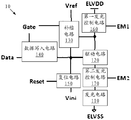
- FIG. 1 is a schematic diagram of a pixel circuit according to an embodiment of the present disclosure
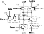
- FIG. 2 is a second schematic diagram of a pixel circuit according to an embodiment of the present disclosure.
- FIG. 3A is a schematic diagram of a pixel circuit shown in FIG. 2 in a state of being turned on in a reset phase according to an embodiment of the present disclosure
- FIG. 3B is a schematic diagram of a pixel circuit shown in FIG. 2 in a state of threshold compensation and data writing in a conductive state according to an embodiment of the present disclosure
- FIG. 3C is a schematic diagram of a pixel circuit shown in FIG. 2 in a voltage-off compensation and light-emitting phase according to an embodiment of the present disclosure
- FIG. 4 is a driving waveform diagram of a pixel circuit shown in FIG. 2 according to an embodiment of the present disclosure
- FIG. 5 is a third schematic diagram of a pixel circuit according to an embodiment of the present disclosure.
- FIG. 6 is a fourth schematic diagram of a pixel circuit according to an embodiment of the present disclosure.
- FIG. 7 is a fifth schematic diagram of a pixel circuit according to an embodiment of the present disclosure.
- FIG. 8 is a sixth schematic diagram of a pixel circuit according to an embodiment of the present disclosure.
- FIG. 9 is a driving waveform diagram of a pixel circuit shown in FIG. 7 or FIG. 8 according to an embodiment of the present disclosure.
- FIG. 10 is a schematic diagram of a display panel according to an embodiment of the present disclosure.
- OLED organic light-emitting diode
- the threshold voltages of the driving transistors in the respective pixel units may differ due to the fabrication process, and the threshold voltage of the driving transistor may also drift due to, for example, the influence of temperature changes. Therefore, the difference in threshold voltages of the respective driving transistors may also cause the display panel to be unevenly displayed. Therefore, this also leads to the need to compensate for the threshold voltage.
- Embodiments of the present disclosure provide a pixel circuit, a display panel, and a driving method, which can perform resistance voltage drop and threshold voltage compensation on the display panel, improve uniformity of driving current, and further improve display uniformity of the display panel.
- an embodiment of the present disclosure provides a pixel circuit 10 including: a lighting circuit 110 for emitting light during operation; a driving circuit 120 for driving the lighting circuit 110; and a compensation circuit 130 for a compensation driving circuit 120; a data writing circuit 140 for driving to the driving circuit 120 Writing data; reset circuit 150 for resetting compensation circuit 130 and driving circuit 120; first lighting control circuit 160 for controlling operation and shutdown of lighting circuit 110; first power supply terminal ELVDD and second power supply terminal ELVSS For supplying the lighting voltage to the lighting circuit 110; resetting the power terminal Vini for providing a reset voltage to the reset circuit 150; the reference power terminal Vref for supplying the compensation voltage to the compensation circuit 130; and scanning the control terminal (Gate) for A signal for controlling the operation and shutdown of the compensation circuit 130 and the data writing circuit 140 is provided; a data signal terminal (Data) for providing a data signal to the data writing circuit 140; and a reset control terminal (Reset) for providing a control reset
- the compensation circuit 130 includes a first transistor T1 and a storage capacitor Cst connected in series with each other, and the data writing circuit 140 includes a series connection with each other.
- OLED organic light emitting diode
- the pixel circuit 10 shown in FIG. 2 is only one example of implementing the pixel circuit 10 shown in FIG. 1. Embodiments of the present disclosure include, but are not limited to, the case shown in FIG. 2.
- the first node S and the second node G are introduced.
- the first node S and the second node G are only used to describe the connection relationship between the components, and are not necessarily in the pixel circuit.
- a solder joint or a pad is set as an actual node.
- the source of the first transistor T1 is electrically connected to the reference power terminal Vref, and the gate of the first transistor T1 is electrically connected to the scan control terminal Gate.
- the drain of the first transistor T1 is electrically connected to the first node S; the source of the second transistor T2 is electrically connected to the data signal terminal Data, the gate of the second transistor T2 is electrically connected to the scan control terminal Gate, and the second transistor T2 is The drain is electrically connected to the source of the third transistor T3; the gate of the third transistor T3 is electrically connected to the drain of the third transistor T3, the drain of the third transistor T3 is electrically connected to the second node G; and the fourth transistor T4 The source is electrically connected to the reset power terminal Vini, the gate of the fourth transistor T4 is electrically connected to the reset control terminal Reset, the drain of the fourth transistor T4 is electrically connected to the second node G, and the source of the fifth transistor T5 is A node S is electrically connected, a gate of the fifth transistor T5 is electrically connected to the second node G; a source of the sixth transistor T6 is electrically connected to the first power terminal ELVDD, and a gate of the sixth transistor T6 is connected to the
- the EM1 is electrically connected, and the sixth transistor T6 is leaked.
- the first end of the storage capacitor Cst is electrically connected to the first node S, and the second end of the storage capacitor Cst is electrically connected to the second node G; the first end of the OLED and the fifth transistor T5 are The drain is electrically connected, and the second end of the OLED is electrically connected to the second power terminal ELVSS.
- the source and the drain of the transistor may be interchanged.
- the first end of the OLED is the anode and the second end of the OLED is the cathode.
- the first end of the OLED may also be a cathode, and the second end of the OLED may also be an anode, which is not limited herein.
- the gate of the third transistor T3 is electrically connected to the drain of the third transistor T3 to constitute a structure similar to a diode.
- the threshold voltage of the third transistor T3 is the same as the threshold voltage of the fifth transistor T5.
- the first transistor T1, the second transistor T2, the third transistor T3, the fourth transistor T4, the fifth transistor T5, and the sixth transistor T6 are all thin film transistors (Thin film transistor). , TFT), but is not limited thereto, and may be, for example, other field effect transistors.
- the first transistor T1, the second transistor T2, the third transistor T3, the fourth transistor T4, the fifth transistor T5, and the sixth transistor T6 are all P-type transistors.
- the embodiments of the present disclosure include, but are not limited to, the case where the first transistor T1, the second transistor T2, the third transistor T3, the fourth transistor T4, the fifth transistor T5, and the sixth transistor T6 are all P-type transistors. .
- some or all of the transistors in the pixel circuit may also be N-type transistors, and the types of the respective transistors may be selected according to actual needs, and the structure and/or the driving method of the pixel circuits are correspondingly changed accordingly.
- an embodiment of the present disclosure further provides a driving method of a pixel circuit, which is described by the pixel circuit shown in FIG. 2.
- FIG. 4 is a driving waveform diagram of a pixel circuit shown in FIG. 2 according to an embodiment of the present disclosure. As shown in FIG. 4, the driving method includes a reset phase t1, a threshold compensation and data writing phase t2, a voltage drop compensation, and an illumination phase t3.
- the reset control terminal Reset in the reset phase t1, the reset control terminal Reset outputs an effective signal, the scan control terminal Gate outputs an invalid signal, and the first lighting control terminal EM1 outputs an invalid signal.
- the reset control terminal Reset outputs an invalid signal
- the scan control terminal Gate outputs an effective signal
- the first lighting control terminal EM1 outputs an invalid signal
- the reset control terminal Reset outputs an invalid signal
- the scan control terminal Gate outputs an invalid signal
- the first lighting control terminal EM1 outputs a valid signal.
- the "effective signal” refers to a signal that enables the transistor to be turned on when the gate of the transistor is loaded, that is, a signal that enables the source and the drain of the transistor to be in an on state, that is, enables the corresponding circuit to operate. signal.
- the effective signal when the transistor is a P-type transistor, the effective signal is a low level signal (ie, a signal lower than the threshold voltage of the transistor); when the transistor is an N-type transistor, the effective signal is a high level signal (ie, higher than the transistor) The signal of the threshold voltage).
- the "invalid signal” refers to a signal that enables the transistor to be turned off when loaded at the gate of the transistor, that is, a signal that enables an open state between the source and the drain of the transistor, that is, enables the corresponding circuit to be turned off. signal of.
- the invalid signal is a high level signal (ie, a signal higher than the threshold voltage of the transistor); when the transistor is an N-type transistor, the invalid signal is a low level signal (ie, lower than the transistor) The signal of the threshold voltage).
- the reset control terminal Reset outputs a valid signal, thereby turning on the fourth transistor T4; the scan control terminal Gate outputs an invalid signal, thereby turning off the first transistor T1, and second.
- the transistor T2 is turned off; the first light-emitting control terminal EM1 outputs an invalid signal, thereby turning off the sixth transistor T6.
- the fourth transistor T4 is turned on, the reset power terminal Vini is turned on by the fourth transistor T4 and the second node G, so that the voltage of the second node G is equal to the reset voltage Vvini provided by the reset power terminal, that is, the storage capacitor in the compensation circuit 130.
- the voltage at the second terminal of Cst is Vvini
- the voltage at the gate of the fifth transistor T5 in the driving circuit 120 is Vvini, that is, in the reset phase t1, the reset circuit 150 resets the compensation circuit 130 and the driving circuit 120.
- the reset control terminal Reset outputs an invalid signal, thereby turning off the fourth transistor T4; the scan control terminal Gate outputs an effective signal, thereby making the first transistor T1
- the second transistor T2 is turned on; the first light-emitting control terminal EM1 outputs an invalid signal, thereby turning off the sixth transistor T6. Since the first transistor T1 is turned on, the reference power terminal Vref is turned on by the first transistor T1 and the first node S, so that the voltage of the first node S is equal to the compensation voltage Vvref provided by the reference power terminal, that is, the power is stored in the compensation circuit 130.
- the voltage of the first terminal of the capacitor Cst is Vvref; since the second transistor T2 is turned on, the data signal terminal Data is connected to the second node G through the second transistor T2 and the third transistor T3, and, due to the gate of the third transistor T3
- the third transistor T3 is electrically connected to the drain.
- the third transistor T3 is equivalent to a diode. Therefore, the voltage of the second node G is the voltage Vdata of the data signal terminal Data plus the threshold voltage Vth of the third transistor T3, that is, the storage capacitor Cst in the compensation circuit 130.
- the voltage of the second terminal is Vdata+Vth
- the voltage of the gate of the fifth transistor T5 in the driving circuit 120 is Vdata+Vth.
- the data write circuit 140 writes data to the drive circuit 120 while performing threshold compensation. At this time, the voltage difference between the second end of the storage capacitor Cst and the first end is Vdata+Vth-Vvref.
- the threshold voltage of the fifth transistor T5 and the threshold voltage of the third transistor T3 are both equal to Vth
- the voltage of the gate of the fifth transistor T5 is Vdata+Vth
- the fifth transistor T5 among the plurality of pixel circuits ie, When the threshold voltage of the driving transistor is different or the threshold voltage is drifted, the gate voltage of the driving transistor is the sum of the threshold voltage of the driving transistor and the voltage Vdata of the data signal terminal Data, that is, the basis of the threshold voltage of the driving transistor is compensated.
- the voltage Vdata on which the data signal terminal Data is superimposed is more effective in the threshold compensation than in the case where the threshold voltage of the fifth transistor T5 is not equal to the threshold voltage of the third transistor T3.
- the reset control terminal Reset outputs an invalid signal, thereby turning off the fourth transistor T4; the scan control terminal Gate outputs an invalid signal, thereby turning off the first transistor T1.
- the second transistor T2 is turned off; the first light-emitting control terminal EM1 outputs an effective signal, thereby turning on the sixth transistor T6.
- the first power supply terminal ELVDD, the sixth transistor T6, the fifth transistor T5, the OLED, and the second power supply terminal ELVSS form a path, and the first power supply terminal ELVDD and the second power supply terminal ELVSS provide a light-emitting voltage to the OLED in the light-emitting circuit 110 (No.
- the OLED in the light emitting circuit 110 emits light under the action of a power supply terminal ELVDD providing a first illuminating voltage Velvdd, a second power supply terminal ELVSS providing a second illuminating voltage Velvss, and a driving of a fifth transistor T5 in the driving circuit 120. Since the sixth transistor T6 is turned on, the first power terminal ELVDD is turned on with the first node S through the sixth transistor T6, so that the voltage of the first node S becomes the first illuminating voltage Velvdd provided by the first power terminal ELVDD, that is, the storage The voltage at the first end of the capacitor Cst is Velvdd, and the voltage at the source of the fifth transistor T5 is Velvdd.
- the gate-source voltage Vgs of the fifth transistor T5 (ie, the difference between the gate voltage and the source voltage of the fifth transistor T5) is as follows:
- the OLED In normal operation, the OLED is in a saturated region, and the driving current Ioled flowing through the OLED satisfies the following equation:
- ⁇ n is the channel mobility of the fifth transistor T5
- Cox is the channel capacitance per unit area of the fifth transistor T5
- W and L are the channel width and the channel length of the fifth transistor T5, respectively.
- the driving current Ioled flowing through the OLED is independent of the threshold voltage Vth of the fifth transistor T5, the first power supply terminal ELVDD provides the first lighting voltage Velvdd, and the second power terminal ELVSS provides the second lighting voltage Velvss;
- the voltage Vdata of the data signal terminal Data and the compensation voltage Vvref provided by the reference power supply terminal Vref are related. As long as the difference between the voltage Vdata of the data signal terminal Data and the compensation voltage Vvref provided by the reference power supply terminal is constant, the driving current Ioled flowing through the OLED is constant. . Therefore, the compensation of the threshold voltage and the resistance voltage drop is realized, the uniformity of the driving current is improved, and the uniformity of display of the display panel is improved.
- the first power supply terminal ELVDD provides the first lighting voltage Velvdd
- the second power terminal ELVSS provides the second lighting voltage Velvss
- the compensation voltage Vvref provided by the reference power terminal Vref
- the reset power terminal Vini is a constant voltage.
- Velvdd 8V
- Velvss -1V
- Vvref 4V
- Vvini -3V
- Vdata 3V
- Cst 0.35PF.
- the difference from the first embodiment is that the pixel circuit provided by this embodiment 10, further comprising: a second illumination control circuit 170 for controlling the operation and the shutdown of the illumination circuit 110; and a second illumination control terminal EM2 for providing a signal for controlling the operation and the shutdown of the second illumination control circuit 170.
- the compensation circuit includes a first transistor T1 and a storage capacitor Cst
- the data writing circuit 140 includes a second transistor T2 and a third transistor T3 connected in series with each other.
- the reset circuit 150 includes a fourth transistor T4
- the drive circuit 120 includes a fifth transistor T5
- the first illumination control circuit 160 includes a sixth transistor T6
- the second illumination control circuit 170 includes a seventh transistor T7
- the illumination circuit includes an OLED.
- the second light emission control circuit 170 and the second light emission control terminal EM2 can avoid a display effect that is deteriorated due to a lightening phenomenon that the OLED in the drive circuit 120 may occur outside the light emission period.
- the first light emission control terminal EM1 and the second light emission control terminal EM2 are electrically connected to each other.
- the first illumination control terminal EM1 and the second illumination control terminal EM2 are both connected to the illumination control terminal EM.
- the source of the first transistor T1 is electrically connected to the reference power terminal Vref, and the gate of the first transistor T1 and the scan control terminal Gate.
- the drain of the first transistor T1 is electrically connected to the first node S; the source of the second transistor T2 is electrically connected to the data signal terminal Data, the gate of the second transistor T2 is electrically connected to the scan control terminal Gate, and the second The drain of the transistor T2 is electrically connected to the source of the third transistor T3; the gate of the third transistor T3 is electrically connected to the drain of the third transistor T3, and the drain of the third transistor T3 is electrically connected to the second node G;
- the source of the fourth transistor T4 is electrically connected to the reset power terminal Vini, the gate of the fourth transistor T4 is electrically connected to the reset control terminal Reset, and the drain of the fourth transistor T4 is electrically connected to the second node G; the source of the fifth transistor T5
- the pole is electrically connected to the first node S, the gate of the fifth transistor T5 is electrically connected to the second node G; the source of the sixth transistor T6 is electrically connected to the first power terminal ELVDD, and the gate of the sixth transistor
- the pole is electrically connected to the second power terminal ELVSS. That is, the positions of the OLED and the seventh transistor T7 are interchangeable and are not limited herein.
- the threshold voltage of the third transistor T3 is the same as the threshold voltage of the fifth transistor T5.
- the first transistor T1, the second transistor T2, the third transistor T3, the fourth transistor T4, the fifth transistor T5, the sixth transistor T6, and the seventh transistor T7 are all thin films. Transistor or other type of field effect transistor.
- the first transistor T1, the second transistor T2, the third transistor T3, the fourth transistor T4, the fifth transistor T5, the sixth transistor T6, and the seventh transistor T7 are all P. Type transistor.
- embodiments of the present disclosure include, but are not limited to, the first transistor T1, the second transistor T2, the third transistor T3, the fourth transistor T4, the fifth transistor T5, the sixth transistor T6, and the seventh transistor T7.
- some or all of the transistors in the pixel circuit may also be N-type transistors, and the types of the respective transistors may be selected according to actual needs, and the structure and/or driving method of the pixel circuits are correspondingly changed accordingly.
- the embodiment of the present disclosure further provides a driving method of the pixel circuit, which is illustrated by the pixel circuit shown in FIG. 7.
- FIG. 9 is a driving of the pixel circuit shown in FIG. 7 or FIG. 8 according to an embodiment of the present disclosure.
- the waveform diagram, as shown in FIG. 9, includes a reset phase t1, a threshold compensation and data writing phase t2, a voltage drop compensation, and an illumination phase t3.
- the reset control terminal Reset in the reset phase, the reset control terminal Reset outputs an effective signal, the scan control terminal Gate outputs an invalid signal, and the first lighting control terminal EM1 and the second lighting control terminal EM2 output an invalid signal. That is, the illumination control terminal EM outputs an invalid signal.
- the reset control terminal Reset outputs an invalid signal
- the scan control terminal Gate outputs an effective signal
- the first illumination control terminal EM1 and the second illumination control terminal The EM2 outputs an invalid signal, that is, the illumination control terminal EM outputs an invalid signal.
- the reset control end Reset outputs an invalid signal
- the scan control end Gate outputs an invalid signal
- the first illumination control The terminal EM1 and the second illumination control terminal EM2 output a valid signal, that is, the illumination control terminal EM outputs a valid signal.
- the reset control terminal Reset outputs an effective signal, thereby turning on the fourth transistor T4; the scan control terminal Gate outputs an invalid signal, thereby turning off the first transistor T1, and second.
- the transistor T2 is turned off; the light-emitting control terminal EM outputs an invalid signal, thereby turning off the sixth transistor T6 and turning off the seventh transistor T7. Since the fourth transistor T4 is turned on, the reset power terminal Vini is turned on by the fourth transistor T4 and the second node G, so that the voltage of the second node G is equal to the reset voltage Vvini provided by the reset power terminal, that is, the storage capacitor in the compensation circuit 130.
- the voltage at the second terminal of Cst is Vvini
- the voltage at the gate of the fifth transistor T5 in the driving circuit 120 is Vvini, that is, in the reset phase t1
- the reset circuit 150 resets the compensation circuit 130 and the driving circuit 120. Since the seventh transistor T7 is turned off, the OLED dim phenomenon which may be caused by the leakage current flowing through the fifth transistor T5 is avoided.
- the reset control terminal Reset outputs an invalid signal, thereby turning off the fourth transistor T4; the scan control terminal Gate outputs an effective signal, thereby turning on the first transistor T1, and the second transistor T2
- the light-emitting control terminal EM outputs an invalid signal, so that the sixth transistor T6 is turned off and the seventh transistor T7 is turned off. Since the first transistor T1 is turned on, the reference power supply terminal Vref is turned on by the first transistor T1 and the first node S, so that the voltage of the first node S is equal to the compensation voltage Vvref provided by the reference power supply terminal, that is, the storage capacitor in the compensation circuit 130.
- the voltage of the first terminal of Cst is Vvref; since the second transistor T2 is turned on, the data signal terminal Data is connected to the second node G through the second transistor T2 and the third transistor T3, and, due to the gate of the third transistor T3 The third transistor T3 is connected to the drain voltage.
- the voltage at the second terminal is Vdata+Vth, and the voltage at the gate of the fifth transistor T5 in the driving circuit 120 is Vdata+Vth. It should be noted that since the voltage of the second node G in the last stage (reset phase t1) is equal to the reset voltage Vvini provided by the reset power supply terminal, Vvini-Vth ⁇ Vdata needs to be satisfied.
- the data write circuit 140 writes data to the drive circuit 120 while performing threshold compensation.
- the voltage difference between the second end of the storage capacitor Cst and the first end is Vdata+Vth-Vvref.
- the fifth crystal The threshold voltage of the tube T5 is equal to the threshold voltage of the third transistor T3, and the effect of the threshold compensation is better. Since the seventh transistor T7 is turned off, the OLED dim phenomenon which may be caused by the leakage current flowing through the fifth transistor T5 is avoided.
- the reset control terminal Reset outputs an invalid signal, thereby turning off the fourth transistor T4; the scan control terminal Gate outputs an invalid signal, thereby turning off the first transistor T1 and closing the second transistor T2.
- the light-emitting control terminal EM outputs an effective signal, so that the sixth transistor T6 is turned on and the seventh transistor is turned on.
- the first power supply terminal ELVDD, the sixth transistor T6, the fifth transistor T5, the seventh transistor T7, the OLED, and the second power supply terminal ELVSS form a path, and the first power supply terminal ELVDD and the second power supply terminal ELVSS are provided to the OLED in the light emitting circuit 110.
- the illuminating voltage (the first power supply terminal ELVDD provides the first illuminating voltage Velvdd, the second power supply terminal ELVSS provides the second illuminating voltage Velvss), and the driving of the fifth transistor T5 in the driving circuit 120, in the illuminating circuit 110 OLED illumination. Since the sixth transistor T6 is turned on, the first power terminal ELVDD is turned on with the first node S through the sixth transistor T6, so that the voltage of the first node S becomes the first illuminating voltage Velvdd provided by the first power terminal ELVDD, that is, the storage The voltage at the first end of the capacitor Cst is Velvdd, and the voltage at the source of the fifth transistor T5 is Velvdd.
- the change of the voltage at the first end causes a change in the voltage of the second terminal, and the voltage difference between the second end and the first end does not change.
- the voltage change at the second end of the storage capacitor Cst is the voltage Velvdd of the first terminal plus the voltage difference between the second end and the first end of the storage capacitor Cst in the previous stage (threshold compensation and data writing phase t2) is Vdata+ Vth-Vvref, that is, the voltage of the second node G is Velvdd+Vdata+Vth-Vvref, and the voltage of the gate of the fifth transistor T5 is Velvdd+Vdata+Vth-Vvref.
- the gate-source voltage Vgs of the fifth transistor T5 ie, the difference between the gate voltage and the source voltage of the fifth transistor T5 is the following equation:
- the OLED In normal operation, the OLED is in a saturated region, and the driving current Ioled flowing through the OLED satisfies the following equation:
- ⁇ n is the channel mobility of the fifth transistor T5
- Cox is the channel capacitance per unit area of the fifth transistor T5
- W and L are the channel width and the channel length of the fifth transistor T5, respectively.
- the driving current Ioled flowing through the OLED is independent of the threshold voltage Vth of the fifth transistor T5, the first power supply terminal ELVDD provides the first lighting voltage Velvdd, and the second power terminal ELVSS provides the second lighting voltage Velvss;
- the voltage Vdata of the data signal terminal Data and the compensation voltage Vvref supplied from the reference power supply terminal are related. As long as the difference between the voltage Vdata of the data signal terminal Data and the compensation voltage Vvref supplied from the reference power supply terminal is constant, the driving current Ioled flowing through the OLED is constant. Therefore, the compensation of the threshold voltage and the resistance voltage drop is realized, the uniformity of the driving current is improved, and the uniformity of display of the display panel is improved.
- an embodiment of the present disclosure further provides a display panel 1 including the pixel circuit 10 and the driving device 20 according to any embodiment of the present disclosure.
- the display panel 1 may include a plurality of pixel circuits 10 arranged in a matrix.
- the display panel 1 provided by the embodiment of the present disclosure further includes a driving device 20, which may be integrated in the circuit of the display panel 1, or a separately prepared driving device (for example, a driving IC) may be mounted on the display panel 1.
- the driving device may be a dedicated hardware device for implementing the driving method described in any of the embodiments of the present disclosure.
- the driving device is configured to be capable of generating a driving waveform of a reset phase t1, a threshold compensation and data writing phase t2, a voltage drop compensation, and an emission phase t3 in the driving method according to any one of the embodiments of the present disclosure.
- the dedicated hardware device can be a PLC, FPGA, ASIC, DSP, or other programmable logic control device.
- the driving device may be a circuit board or a combination of a plurality of circuit boards for implementing the driving method as described above.
- the one circuit board or a combination of the plurality of circuit boards may include: (1) one or more processors; (2) one or more non-transitory computers connected to the processor Read memory; and/or (3) firmware stored in memory.
- the display panel provided by the embodiment of the present disclosure can be used for any product or component having a display function, such as a mobile phone, a tablet computer, a television, a display, a notebook computer, a digital photo frame, a navigator, and the like.
- Embodiments of the present disclosure provide a pixel circuit, a display panel, and a driving method, which are applicable to a display surface
- the board performs resistance voltage drop and threshold voltage compensation, which improves the uniformity of the driving current, thereby improving the uniformity of display of the display panel.
Landscapes
- Engineering & Computer Science (AREA)
- Physics & Mathematics (AREA)
- Computer Hardware Design (AREA)
- General Physics & Mathematics (AREA)
- Theoretical Computer Science (AREA)
- Electroluminescent Light Sources (AREA)
- Control Of El Displays (AREA)
- Control Of Indicators Other Than Cathode Ray Tubes (AREA)
Abstract
一种像素电路(10)、显示面板(1)和驱动方法。像素电路(10)包括:用于在工作时发光的发光电路(110);用于驱动发光电路(110)的驱动电路(120);用于补偿驱动电路(120)的补偿电路(130);用于向驱动电路(120)写入数据的数据写入电路(140);用于将补偿电路(130)和驱动电路(120)复位的复位电路(150);用于控制发光电路(110)的工作和关断的第一发光控制电路(160)。可对显示面板(1)进行电阻压降和阈值电压(Vth)补偿,提高了驱动电流(Ioled)的均匀性,进而提高了显示面板(1)显示的均匀性。
Description
本公开的实施例涉及一种像素电路、显示面板及驱动方法。
在显示领域,有机电致发光二极管(OLED)显示面板具有自发光、对比度高、厚度薄、视角广、反应速度快、可用于挠曲性面板、使用温度范围广、制造简单等特点,具有广阔的发展前景。
由于上述特点,有机电致发光二极管(OLED)显示面板可以适用于手机、显示器、笔记本电脑、数码相机、仪器仪表等具有显示功能的装置。
发明内容
本公开的实施例提供一种像素电路,包括:发光电路,用于在工作时发光;驱动电路,用于驱动所述发光电路;补偿电路,用于补偿所述驱动电路;数据写入电路,用于向所述驱动电路写入数据;复位电路,用于将所述补偿电路和所述驱动电路复位;第一发光控制电路,用于控制所述发光电路的工作和关断;第一电源端和第二电源端,用于向所述发光电路提供发光电压;复位电源端,用于向所述复位电路提供复位电压;参考电源端,用于向所述补偿电路提供补偿电压;扫描控制端,用于提供控制所述补偿电路和所述数据写入电路的工作和关断的信号;数据信号端,用于向所述数据写入电路提供数据信号;复位控制端,用于提供控制所述复位电路的工作和关断的信号;以及第一发光控制端,用于提供控制所述第一发光控制电路的工作和关断的信号。
例如,在本公开实施例提供的像素电路中,所述补偿电路包括彼此串联的第一晶体管和存储电容,所述数据写入电路包括彼此串联的第二晶体管和第三晶体管,所述复位电路包括第四晶体管,所述驱动电路包括第五晶体管,所述第一发光控制电路包括第六晶体管,所述发光电路包括有机发光二极管。
例如,在本公开实施例提供的像素电路中,所述第一晶体管的源极与所
述参考电源端电连接,所述第一晶体管的栅极与所述扫描控制端电连接,所述第一晶体管的漏极与第一节点电连接;所述第二晶体管的源极与所述数据信号端电连接,所述第二晶体管的栅极与所述扫描控制端电连接,所述第二晶体管的漏极与所述第三晶体管的源极电连接;所述第三晶体管的栅极与所述第三晶体管的漏极电连接,所述第三晶体管的漏极与第二节点电连接;所述第四晶体管的源极与所述复位电源端电连接,所述第四晶体管的栅极与所述复位控制端电连接,所述第四晶体管的漏极与所述第二节点电连接;所述第五晶体管的源极与所述第一节点电连接,所述第五晶体管的栅极与所述第二节点电连接;所述第六晶体管的源极与所述第一电源端电连接,所述第六晶体管的栅极与所述第一发光控制端电连接,所述第六晶体管的漏极与所述第一节点电连接;所述存储电容的第一端与所述第一节点电连接,所述存储电容的第二端与所述第二节点电连接;所述有机发光二极管的第一端与所述第五晶体管的漏极电连接,所述有机发光二极管的第二端与所述第二电源端电连接。
例如,本公开实施例提供的像素电路,还包括:第二发光控制电路,用于控制所述发光电路的工作和关断;以及第二发光控制端,用于提供控制所述第二发光控制电路的工作和关断的信号。
例如,在本公开实施例提供的像素电路中,所述第一发光控制端和所述第二发光控制端彼此电连接。
例如,在本公开实施例提供的像素电路中,所述补偿电路包括第一晶体管和存储电容,所述数据写入电路包括彼此串联的第二晶体管和第三晶体管,所述复位电路包括第四晶体管,所述驱动电路包括第五晶体管,所述第一发光控制电路包括第六晶体管,所述第二发光控制电路包括第七晶体管,所述发光电路包括有机发光二极管。
例如,在本公开实施例提供的像素电路中,所述第一晶体管的源极与所述参考电源端电连接,所述第一晶体管的栅极与所述扫描控制端电连接,所述第一晶体管的漏极与第一节点电连接;所述第二晶体管的源极与所述数据信号端电连接,所述第二晶体管的栅极与所述扫描控制端电连接,所述第二晶体管的漏极与所述第三晶体管的源极电连接;所述第三晶体管的栅极与所述第三晶体管的漏极电连接,所述第三晶体管的漏极与第二节点电连接;所
述第四晶体管的源极与所述复位电源端电连接,所述第四晶体管的栅极与所述复位控制端电连接,所述第四晶体管的漏极与所述第二节点电连接;所述第五晶体管的源极与所述第一节点电连接,所述第五晶体管的栅极与所述第二节点电连接;所述第六晶体管的源极与所述第一电源端电连接,所述第六晶体管的栅极与所述第一发光控制端电连接,所述第六晶体管的漏极与所述第一节点电连接;所述存储电容的第一端与所述第一节点电连接,所述存储电容的第二端与所述第二节点电连接;所述第七晶体管的源极与所述第五晶体管的漏极电连接,所述第七晶体管的栅极与所述第二发光控制端电连接,所述有机发光二极管的第一端与所述第七晶体管的漏极电连接,所述有机发光二极管的第二端与所述第二电源端电连接;或者,所述有机发光二极管的第一端与所述第五晶体管的漏极电连接,所述有机发光二极管的第二端与所述第七晶体管的源极电连接,所述第七晶体管的栅极与所述第二发光控制端电连接,所述第七晶体管的漏极与所述第二电源端电连接。
例如,在本公开实施例提供的像素电路中,所述第三晶体管的阈值电压与所述第五晶体管的阈值电压相同。
例如,在本公开实施例提供的像素电路中,所述第一晶体管、所述第二晶体管、所述第三晶体管、所述第四晶体管、所述第五晶体管、所述第六晶体管以及所述第七晶体管均为薄膜晶体管。
例如,在本公开实施例提供的像素电路中,所述第一晶体管、所述第二晶体管、所述第三晶体管、所述第四晶体管、所述第五晶体管、所述第六晶体管以及所述第七晶体管均为P型晶体管。
本公开的实施例还提供一种显示面板,其包括本公开任一实施例所述的像素电路。
本公开的实施例还提供一种像素电路的驱动方法,所述像素电路包括:发光电路,用于在工作时发光;驱动电路,用于驱动所述发光电路;补偿电路,用于补偿所述驱动电路;数据写入电路,用于向所述驱动电路写入数据;复位电路,用于将所述补偿电路和所述驱动电路复位;第一发光控制电路,用于控制所述发光电路的工作和关断;第一电源端和第二电源端,用于向所述发光电路提供发光电压;复位电源端,用于向所述复位电路提供复位电压;参考电源端,用于向所述补偿电路提供补偿电压;扫描控制端,用于提供控
制所述补偿电路和所述数据写入电路的工作和关断的信号;数据信号端,用于向所述数据写入电路提供数据信号;复位控制端,用于提供控制所述复位电路的工作和关断的信号;以及第一发光控制端,用于提供控制所述第一发光控制电路的工作和关断的信号,所述驱动方法包括复位阶段、阈值补偿及数据写入阶段、压降补偿及发光阶段。
例如,在本公开实施例提供的驱动方法中,在所述复位阶段,所述复位控制端输出有效信号,所述扫描控制端输出无效信号,所述第一发光控制端输出无效信号。
例如,在本公开实施例提供的驱动方法中,在所述阈值补偿及数据写入阶段,所述复位控制端输出无效信号,所述扫描控制端输出有效信号,所述第一发光控制端输出无效信号。
例如,在本公开实施例提供的驱动方法中,在所述压降补偿及发光阶段,所述复位控制端输出无效信号,所述扫描控制端输出无效信号,所述第一发光控制端输出有效信号。
本公开的实施例还提供一种像素电路的驱动方法,所述像素电路包括:发光电路,用于在工作时发光;驱动电路,用于驱动所述发光电路;补偿电路,用于补偿所述驱动电路;数据写入电路,用于向所述驱动电路写入数据;复位电路,用于将所述补偿电路和所述驱动电路复位;第一发光控制电路,用于控制所述发光电路的工作和关断;第一电源端和第二电源端,用于向所述发光电路提供发光电压;复位电源端,用于向所述复位电路提供复位电压;参考电源端,用于向所述补偿电路提供补偿电压;扫描控制端,用于提供控制所述补偿电路和所述数据写入电路的工作和关断的信号;数据信号端,用于向所述数据写入电路提供数据信号;复位控制端,用于提供控制所述复位电路的工作和关断的信号;以及第一发光控制端,用于提供控制所述第一发光控制电路的工作和关断的信号;第二发光控制电路,用于控制所述发光电路的工作和关断;以及第二发光控制端,用于提供控制所述第二发光控制电路的工作和关断的信号,所述驱动方法包括复位阶段、阈值补偿及数据写入阶段、压降补偿及发光阶段。
例如,在本公开实施例提供的驱动方法中,在所述复位阶段,所述复位控制端输出有效信号,所述扫描控制端输出无效信号,所述第一发光控制端
和所述第二发光控制端输出无效信号。
例如,在本公开实施例提供的驱动方法中,在所述阈值补偿及数据写入阶段,所述复位控制端输出无效信号,所述扫描控制端输出有效信号,所述第一发光控制端和所述第二发光控制端输出无效信号。
例如,在本公开实施例提供的驱动方法中,在所述压降补偿及发光阶段,所述复位控制端输出无效信号,所述扫描控制端输出无效信号,所述第一发光控制端和所述第二发光控制端输出有效信号。
为了更清楚地说明本公开实施例的技术方案,下面将对实施例或相关技术描述中所需要使用的附图作简单地介绍,显而易见地,下面描述中的附图仅仅涉及本公开的一些实施例,并非对本公开的限制。
图1是本公开实施例提供的一种像素电路的示意图之一;
图2是本公开实施例提供的一种像素电路的示意图之二;
图3A是本公开实施例提供的一种如图2所示的像素电路在复位阶段导通状态的示意图;
图3B是本公开实施例提供的一种如图2所示的像素电路在阈值补偿及数据写入阶段导通状态的示意图;
图3C是本公开实施例提供的一种如图2所示的像素电路在压降补偿及发光阶段导通状态的示意图;
图4是本公开实施例提供的一种如图2所示的像素电路的驱动波形图;
图5是本公开实施例提供的一种像素电路的示意图之三;
图6是本公开实施例提供的一种像素电路的示意图之四;
图7是本公开实施例提供的一种像素电路的示意图之五;
图8是本公开实施例提供的一种像素电路的示意图之六;
图9是本公开实施例提供的一种如图7或图8所示的像素电路的驱动波形图;以及
图10是本公开实施例提供的一种显示面板的示意图。
下面将结合附图,对本公开实施例中的技术方案进行清楚、完整地描述参考在附图中示出并在以下描述中详述的非限制性示例实施例,更加全面地说明本公开的示例实施例和它们的多种特征及有利细节。应注意的是,图中示出的特征不是必须按照比例绘制。本公开省略了已知材料、组件和工艺技术的描述,从而不使本公开的示例实施例模糊。所给出的示例仅旨在有利于理解本公开示例实施例的实施,以及进一步使本领域技术人员能够实施示例实施例。因而,这些示例不应被理解为对本公开的实施例的范围的限制。
除非另外特别定义,本公开使用的技术术语或者科学术语应当为本公开所属领域内具有一般技能的人士所理解的通常意义。本公开中使用的“第一”、“第二”以及类似的词语并不表示任何顺序、数量或者重要性,而只是用来区分不同的组成部分。此外,在本公开各个实施例中,相同或类似的参考标号表示相同或类似的构件。
在有机发光二极管(Organic Light-Emitting Diode,OLED)显示面板中,会存在电阻压降(IR drop)现象,电阻压降是由于显示面板中导线的自身电阻分压造成的,即电流经过显示面板中的导线时,根据欧姆定律,导线上会产生一定的电压降。因此,位于不同位置的像素单元受到电阻压降影响的程度也不相同,这会导致显示面板显示不均匀。因此,需要对OLED显示面板中的电阻压降进行补偿。
而且,在OLED显示面板中,各个像素单元中的驱动晶体管的阈值电压由于制备工艺可能存在差异,而且由于例如温度变化的影响,驱动晶体管的阈值电压也会产生漂移的现象。因此,各个驱动晶体管的阈值电压的不同也可能会导致显示面板显示不均匀。因此,这样也导致需要对阈值电压进行补偿。
本公开的实施例提供一种像素电路、显示面板及驱动方法,可对显示面板进行电阻压降和阈值电压补偿,提高了驱动电流的均匀性,进而提高了显示面板显示的均匀性。
第一实施例
例如,如图1所示,本公开的实施例提供一种像素电路10,包括:发光电路110,用于在工作时发光;驱动电路120,用于驱动发光电路110;补偿电路130,用于补偿驱动电路120;数据写入电路140,用于向驱动电路120
写入数据;复位电路150,用于将补偿电路130和驱动电路120复位;第一发光控制电路160,用于控制发光电路110的工作和关断;第一电源端ELVDD和第二电源端ELVSS,用于向发光电路110提供发光电压;复位电源端Vini,用于向复位电路150提供复位电压;参考电源端Vref,用于向补偿电路130提供补偿电压;扫描控制端(Gate),用于提供控制补偿电路130和数据写入电路140的工作和关断的信号;数据信号端(Data),用于向数据写入电路140提供数据信号;复位控制端(Reset),用于提供控制复位电路150的工作和关断的信号;第一发光控制端EM1,用于提供控制第一发光控制电路160的工作和关断的信号。
例如,如图2所示,在本公开实施例提供的像素电路10的一个具体示例中,补偿电路130包括彼此串联的第一晶体管T1和存储电容Cst,数据写入电路140包括彼此串联的第二晶体管T2和第三晶体管T3,复位电路150包括第四晶体管T4,驱动电路120包括第五晶体管T5,第一发光控制电路160包括第六晶体管T6,发光电路110包括有机发光二极管(OLED)。
需要说明的是,图2所示的像素电路10只是实现图1所示的像素电路10的一个示例,本公开的实施例包括但不局限于图2所示的情形。
例如,如图2所示,为方便描述,引入第一节点S和第二节点G,第一节点S和第二节点G只是用于描述各元件之间的连接关系,并非一定要在像素电路10中设置例如焊点或焊盘作为实际的节点。
例如,如图2所示,在本公开实施例提供的像素电路10中,第一晶体管T1的源极与参考电源端Vref电连接,第一晶体管T1的栅极与扫描控制端Gate电连接,第一晶体管T1的漏极与第一节点S电连接;第二晶体管T2的源极与数据信号端Data电连接,第二晶体管T2的栅极与扫描控制端Gate电连接,第二晶体管T2的漏极与第三晶体管T3的源极电连接;第三晶体管T3的栅极与第三晶体管T3的漏极电连接,第三晶体管T3的漏极与第二节点G电连接;第四晶体管T4的源极与复位电源端Vini电连接,第四晶体管T4的栅极与复位控制端Reset电连接,第四晶体管T4的漏极与第二节点G电连接;第五晶体管T5的源极与第一节点S电连接,第五晶体管T5的栅极与第二节点G电连接;第六晶体管T6的源极与第一电源端ELVDD电连接,第六晶体管T6的栅极与第一发光控制端EM1电连接,第六晶体管T6的漏
极与第一节点S电连接;存储电容Cst的第一端与第一节点S电连接,存储电容Cst的第二端与第二节点G电连接;OLED的第一端与第五晶体管T5的漏极电连接,OLED的第二端与第二电源端ELVSS电连接。
需要说明的是,在本公开的实施例中,晶体管的源极和漏极可以互换。
例如,如图所示,OLED的第一端为阳极,OLED的第二端为阴极。根据第一电源端ELVDD和第二电源端ELVSS电压的不同情况,OLED的第一端也可以为阴极,OLED的第二端也可以为阳极,在此不做限定。
例如,第三晶体管T3的栅极与第三晶体管T3的漏极电连接,构成类似于一个二极管的结构。
例如,在本公开实施例提供的像素电路中,第三晶体管T3的阈值电压与第五晶体管T5的阈值电压相同。
例如,在本公开实施例提供的像素电路中,第一晶体管T1、第二晶体管T2、第三晶体管T3、第四晶体管T4、第五晶体管T5以及第六晶体管T6均为薄膜晶体管(Thin film transistor,TFT),但不限于此,例如也可以为其他场效应晶体管。
例如,在本公开实施例提供的像素电路中,第一晶体管T1、第二晶体管T2、第三晶体管T3、第四晶体管T4、第五晶体管T5以及第六晶体管T6均为P型晶体管。
需要说明的是,本公开的实施例包括但不仅限于第一晶体管T1、第二晶体管T2、第三晶体管T3、第四晶体管T4、第五晶体管T5以及第六晶体管T6均为P型晶体管的情形。本公开的实施例中,像素电路中的部分或者所有晶体管也可以为N型晶体管,并且可以根据实际需要选择各个晶体管的类型,相应地对像素电路的结构和/或驱动方法进行相应的改变。
例如,本公开的实施例还提供一种像素电路的驱动方法,以图2所示的像素电路进行说明。图4是本公开实施例提供的一种如图2所示的像素电路的驱动波形图。如图4所示,该驱动方法包括复位阶段t1、阈值补偿及数据写入阶段t2、压降补偿及发光阶段t3。
例如,在本公开实施例提供的驱动方法中,在复位阶段t1,复位控制端Reset输出有效信号,扫描控制端Gate输出无效信号,第一发光控制端EM1输出无效信号。
例如,在本公开实施例提供的驱动方法中,在阈值补偿及数据写入阶段,复位控制端Reset输出无效信号,扫描控制端Gate输出有效信号,第一发光控制端EM1输出无效信号。
例如,在本公开实施例提供的驱动方法中,在压降补偿及发光阶段,复位控制端Reset输出无效信号,扫描控制端Gate输出无效信号,第一发光控制端EM1输出有效信号。
这里,“有效信号”是指加载在晶体管的栅极时能使晶体管开启的信号,即能使晶体管的源极和漏极之间处于导通状态的信号,也就是说能使相应电路工作的信号。例如,当晶体管为P型晶体管时,有效信号为低电平信号(即低于该晶体管阈值电压的信号);当晶体管为N型晶体管时,有效信号为高电平信号(即高于该晶体管阈值电压的信号)。
这里,“无效信号”是指加载在晶体管的栅极时能使晶体管关断的信号,即能使晶体管的源极和漏极之间处于断路状态的信号,也就是说能使相应电路关断的信号。例如,当晶体管为P型晶体管时,无效信号为高电平信号(即高于该晶体管阈值电压的信号);当晶体管为N型晶体管时,无效信号为低电平信号(即低于该晶体管阈值电压的信号)。
例如,参阅图3A和图4,在复位阶段t1,复位控制端Reset输出有效信号,从而使第四晶体管T4导通;扫描控制端Gate输出无效信号,从而使第一晶体管T1关断、第二晶体管T2关断;第一发光控制端EM1输出无效信号,从而使第六晶体管T6关断。由于第四晶体管T4导通,复位电源端Vini通过第四晶体管T4与第二节点G导通,使得第二节点G的电压等于复位电源端提供的复位电压Vvini,即使得补偿电路130中存储电容Cst的第二端的电压为Vvini,驱动电路120中第五晶体管T5栅极的电压为Vvini,也就是说,在复位阶段t1,复位电路150将补偿电路130和驱动电路120复位。
例如,参阅图3B和图4,在阈值补偿及数据写入阶段t2,复位控制端Reset输出无效信号,从而使第四晶体管T4关断;扫描控制端Gate输出有效信号,从而使第一晶体管T1导通、第二晶体管T2导通;第一发光控制端EM1输出无效信号,从而使第六晶体管T6关断。由于第一晶体管T1导通,参考电源端Vref通过第一晶体管T1与第一节点S导通,使得第一节点S的电压等于参考电源端提供的补偿电压Vvref,即使得补偿电路130中存储电
容Cst的第一端的电压为Vvref;由于第二晶体管T2导通,数据信号端Data通过第二晶体管T2和第三晶体管T3与第二节点G连接,并且,由于第三晶体管T3的栅极和漏极电连接,第三晶体管T3相当于一个二极管,因此,第二节点G的电压为数据信号端Data的电压Vdata加上第三晶体管T3的阈值电压Vth,即补偿电路130中存储电容Cst的第二端的电压为Vdata+Vth,驱动电路120中第五晶体管T5栅极的电压为Vdata+Vth。需要说明的是,由于上个阶段(复位阶段t1)第二节点G的电压等于复位电源端提供的复位电压Vvini,需要满足Vvini-Vth<Vdata。这样,在阈值补偿及数据写入阶段t2,数据写入电路140向驱动电路120写入了数据,同时进行了阈值补偿。此时,存储电容Cst第二端和第一端之间的电压差为Vdata+Vth-Vvref。例如,当第五晶体管T5的阈值电压与第三晶体管T3的阈值电压相等均为Vth,这样,第五晶体管T5栅极的电压为Vdata+Vth,当多个像素电路中第五晶体管T5(即驱动晶体管)的阈值电压不同或阈值电压漂移时,驱动晶体管的栅极电压为驱动晶体管的阈值电压与数据信号端Data的电压Vdata之和,也就是说,在补偿了驱动晶体管的阈值电压的基础上叠加了数据信号端Data的电压Vdata,相比于第五晶体管T5的阈值电压与第三晶体管T3的阈值电压不相等的情形,阈值补偿的效果更好。
例如,参阅图3C和图4,在压降补偿及发光阶段t3,复位控制端Reset输出无效信号,从而使第四晶体管T4关断;扫描控制端Gate输出无效信号,从而使第一晶体管T1关断、第二晶体管T2关断;第一发光控制端EM1输出有效信号,从而使第六晶体管T6导通。第一电源端ELVDD、第六晶体管T6、第五晶体管T5、OLED和第二电源端ELVSS形成通路,在第一电源端ELVDD和第二电源端ELVSS向发光电路110中OLED提供的发光电压(第一电源端ELVDD提供第一发光电压Velvdd,第二电源端ELVSS提供第二发光电压Velvss)的作用下,以及驱动电路120中第五晶体管T5的驱动下,发光电路110中的OLED发光。由于第六晶体管T6导通,第一电源端ELVDD通过第六晶体管T6与第一节点S导通,使得第一节点S的电压变为第一电源端ELVDD提供的第一发光电压Velvdd,即存储电容Cst第一端的电压为Velvdd,第五晶体管T5源极的电压为Velvdd。由于存储电容Cst的自举效应,即存储电容Cst存储的电荷没有发生变化时,其第一端电压的变化会引
起第二端电压的变化,且第二端与第一端的电压差不变,存储电容Cst第二端的电压变化为第一端的电压Velvdd加上上一阶段(阈值补偿及数据写入阶段t2)中存储电容Cst第二端和第一端之间的电压差为Vdata+Vth-Vvref,也就是说,此时,第二节点G的电压为Velvdd+Vdata+Vth-Vvref,第五晶体管T5栅极的电压为Velvdd+Vdata+Vth-Vvref。此时,第五晶体管T5的栅源电压Vgs(即第五晶体管T5栅极电压与源极电压之差)为如下等式:
Vgs=Velvdd+Vdata+Vth-Vvref-Velvdd=Vdata+Vth-Vvref
在正常工作时,OLED处于饱和区,流过OLED的驱动电流Ioled满足如下等式:

其中,μn为第五晶体管T5的沟道迁移率,Cox为第五晶体管T5单位面积的沟道电容,W和L分别为第五晶体管T5的沟道宽度和沟道长度。
根据之前的计算,
Vgs-Vth=Vdata+Vth-Vvref-Vth=Vdata-Vvref
因此,

由上式可知,流过OLED的驱动电流Ioled与第五晶体管T5的阈值电压Vth、第一电源端ELVDD提供第一发光电压Velvdd以及第二电源端ELVSS提供第二发光电压Velvss均无关;仅与数据信号端Data的电压Vdata以及参考电源端Vref提供的补偿电压Vvref有关,只要数据信号端Data的电压Vdata与参考电源端提供的补偿电压Vvref之差恒定,则流过OLED的驱动电流Ioled就恒定。因此,实现了对阈值电压以及电阻压降的补偿,提高了驱动电流的均匀性,进而提高了显示面板显示的均匀性。
例如,在本公开的实施例中,第一电源端ELVDD提供第一发光电压Velvdd、第二电源端ELVSS提供第二发光电压Velvss、参考电源端Vref提供的补偿电压Vvref以及复位电源端Vini提供的复位电压均为恒定电压。
例如,在本公开的实施例的一个示例中,Velvdd=8V,Velvss=-1V,Vvref=4V,Vvini=-3V,Vdata=3V,Cst=0.35PF。
第二实施例
如图5所示,与第一实施例的区别之处在于,本实施例提供的像素电路
10,还包括:第二发光控制电路170,用于控制发光电路110的工作和关断;第二发光控制端EM2,用于提供控制第二发光控制电路170的工作和关断的信号。
例如,如图6所示,在本公开实施例提供的像素电路10中,补偿电路包括第一晶体管T1和存储电容Cst,数据写入电路140包括彼此串联的第二晶体管T2和第三晶体管T3,复位电路150包括第四晶体管T4,驱动电路120包括第五晶体管T5,第一发光控制电路160包括第六晶体管T6,第二发光控制电路170包括第七晶体管T7,发光电路包括OLED。
例如,第二发光控制电路170和第二发光控制端EM2可以避免驱动电路120中的OLED在发光时间段之外可能发生的微亮现象而导致的显示效果变差。
例如,如图7所示,在本公开实施例提供的像素电路10中,第一发光控制端EM1和第二发光控制端EM2彼此电连接。例如,第一发光控制端EM1和第二发光控制端EM2均连接至发光控制端EM。
例如,如图7、图8所示,在本公开实施例提供的像素电路10中,第一晶体管T1的源极与参考电源端Vref电连接,第一晶体管T1的栅极与扫描控制端Gate电连接,第一晶体管T1的漏极与第一节点S电连接;第二晶体管T2的源极与数据信号端Data电连接,第二晶体管T2的栅极与扫描控制端Gate电连接,第二晶体管T2的漏极与第三晶体管T3的源极电连接;第三晶体管T3的栅极与第三晶体管T3的漏极电连接,第三晶体管T3的漏极与第二节点G电连接;第四晶体管T4的源极与复位电源端Vini电连接,第四晶体管T4的栅极与复位控制端Reset电连接,第四晶体管T4的漏极与第二节点G电连接;第五晶体管T5的源极与第一节点S电连接,第五晶体管T5的栅极与第二节点G电连接;第六晶体管T6的源极与第一电源端ELVDD电连接,第六晶体管T6的栅极与第一发光控制端EM1电连接,第六晶体管T6的漏极与第一节点S电连接;存储电容Cst的第一端与第一节点S电连接,存储电容Cst的第二端与第二节点G电连接;如图7所示,第七晶体管T7的源极与第五晶体管T5的漏极电连接,第七晶体管T7的栅极与第二发光控制端EM2电连接,OLED的第一端与第七晶体管T7的漏极电连接,OLED的第二端与第二电源端ELVSS电连接;或者,如图8所示,OLED的第一端
与第五晶体管T5的漏极电连接,OLED的第二端与第七晶体管T7的源极电连接,第七晶体管T7的栅极与第二发光控制端EM2电连接,第七晶体管T7的漏极与第二电源端ELVSS电连接。也就是说,OLED和第七晶体管T7的位置可以互换,在此不做限定。
例如,在本公开实施例提供的像素电路中,第三晶体管T3的阈值电压与第五晶体管T5的阈值电压相同。
例如,在本公开实施例提供的像素电路中,第一晶体管T1、第二晶体管T2、第三晶体管T3、第四晶体管T4、第五晶体管T5、第六晶体管T6以及第七晶体管T7均为薄膜晶体管或其他类型的场效应晶体管。
例如,在本公开实施例提供的像素电路中,第一晶体管T1、第二晶体管T2、第三晶体管T3、第四晶体管T4、第五晶体管T5、第六晶体管T6以及第七晶体管T7均为P型晶体管。
需要说明的是,本公开的实施例包括但不仅限于第一晶体管T1、第二晶体管T2、第三晶体管T3、第四晶体管T4、第五晶体管T5、第六晶体管T6以及第七晶体管T7均为P型晶体管的情形,像素电路中的部分或者所有晶体管也可以为N型晶体管,并且可以根据实际需要选择各个晶体管的类型,相应地对像素电路的结构和/或驱动方法进行相应的改变。
本公开的实施例还提供一种像素电路的驱动方法,以图7所示的像素电路进行说明,图9是本公开实施例提供的一种如图7或图8所示的像素电路的驱动波形图,如图9所示,该驱动方法包括复位阶段t1、阈值补偿及数据写入阶段t2、压降补偿及发光阶段t3。
例如,在本公开实施例提供的驱动方法中,在复位阶段,复位控制端Reset输出有效信号,扫描控制端Gate输出无效信号,第一发光控制端EM1和第二发光控制端EM2输出无效信号,即发光控制端EM输出无效信号。
例如,在本公开实施例提供的驱动方法中,在阈值补偿及数据写入阶段,复位控制端Reset输出无效信号,扫描控制端Gate输出有效信号,第一发光控制端EM1和第二发光控制端EM2输出无效信号,即发光控制端EM输出无效信号。
例如,在本公开实施例提供的驱动方法中,在压降补偿及发光阶段,复位控制端Reset输出无效信号,扫描控制端Gate输出无效信号,第一发光控
制端EM1和第二发光控制端EM2输出有效信号,即发光控制端EM输出有效信号。
关于有效信号和无效信号的含义请参照第一实施例中的描述,在此不再赘述。
例如,参阅图7和图9,在复位阶段t1,复位控制端Reset输出有效信号,从而使第四晶体管T4导通;扫描控制端Gate输出无效信号,从而使第一晶体管T1关断、第二晶体管T2关断;发光控制端EM输出无效信号,从而使第六晶体管T6关断、第七晶体管T7关断。由于第四晶体管T4导通,复位电源端Vini通过第四晶体管T4与第二节点G导通,使得第二节点G的电压等于复位电源端提供的复位电压Vvini,即使得补偿电路130中存储电容Cst的第二端的电压为Vvini,驱动电路120中第五晶体管T5栅极的电压为Vvini,也就是说,在复位阶段t1,复位电路150将补偿电路130和驱动电路120复位。由于第七晶体管T7关断,避免了可能由于流过第五晶体管T5的漏电流造成的OLED微亮现象。
例如,在阈值补偿及数据写入阶段t2,复位控制端Reset输出无效信号,从而使第四晶体管T4关断;扫描控制端Gate输出有效信号,从而使第一晶体管T1导通、第二晶体管T2导通;发光控制端EM输出无效信号,从而使第六晶体管T6关断、第七晶体管T7关断。由于第一晶体管T1导通,参考电源端Vref通过第一晶体管T1与第一节点S导通,使得第一节点S的电压等于参考电源端提供的补偿电压Vvref,即使得补偿电路130中存储电容Cst的第一端的电压为Vvref;由于第二晶体管T2导通,数据信号端Data通过第二晶体管T2和第三晶体管T3与第二节点G连接,并且,由于第三晶体管T3的栅极和漏极电连接,第三晶体管T3相当于一个二极管,因此,第二节点G的电压为数据信号端Data的电压Vdata加上第三晶体管T3的阈值电压Vth,即补偿电路130中存储电容Cst的第二端的电压为Vdata+Vth,驱动电路120中第五晶体管T5栅极的电压为Vdata+Vth。需要说明的是,由于上个阶段(复位阶段t1)第二节点G的电压等于复位电源端提供的复位电压Vvini,需要满足Vvini-Vth<Vdata。这样,在阈值补偿及数据写入阶段t2,数据写入电路140向驱动电路120写入了数据,同时进行了阈值补偿。此时,存储电容Cst第二端和第一端之间的电压差为Vdata+Vth-Vvref。例如,当第五晶体
管T5的阈值电压与第三晶体管T3的阈值电压相等均为Vth,此时,阈值补偿的效果更好。由于第七晶体管T7关断,避免了可能由于流过第五晶体管T5的漏电流造成的OLED微亮现象。
例如,在压降补偿及发光阶段t3,复位控制端Reset输出无效信号,从而使第四晶体管T4关断;扫描控制端Gate输出无效信号,从而使第一晶体管T1关断、第二晶体管T2关断;发光控制端EM输出有效信号,从而使第六晶体管T6导通、第七晶体管导通。第一电源端ELVDD、第六晶体管T6、第五晶体管T5、第七晶体管T7、OLED和第二电源端ELVSS形成通路,在第一电源端ELVDD和第二电源端ELVSS向发光电路110中OLED提供的发光电压(第一电源端ELVDD提供第一发光电压Velvdd,第二电源端ELVSS提供第二发光电压Velvss)的作用下,以及驱动电路120中第五晶体管T5的驱动下,发光电路110中的OLED发光。由于第六晶体管T6导通,第一电源端ELVDD通过第六晶体管T6与第一节点S导通,使得第一节点S的电压变为第一电源端ELVDD提供的第一发光电压Velvdd,即存储电容Cst第一端的电压为Velvdd,第五晶体管T5源极的电压为Velvdd。由于存储电容Cst的自举效应,即存储电容Cst存储的电荷没有发生变化时,其第一端电压的变化会引起第二端电压的变化,且第二端与第一端的电压差不变,存储电容Cst第二端的电压变化为第一端的电压Velvdd加上上一阶段(阈值补偿及数据写入阶段t2)中存储电容Cst第二端和第一端之间的电压差为Vdata+Vth-Vvref,也就是说,第二节点G的电压为Velvdd+Vdata+Vth-Vvref,第五晶体管T5栅极的电压为Velvdd+Vdata+Vth-Vvref。此时,第五晶体管T5的栅源电压Vgs(即第五晶体管T5栅极电压与源极电压之差)为下面的等式:
Vgs=Velvdd+Vdata+Vth-Vvref-Velvdd=Vdata+Vth-Vvref
在正常工作时,OLED处于饱和区,流过OLED的驱动电流Ioled满足下面的等式:

其中,μn为第五晶体管T5的沟道迁移率,Cox为第五晶体管T5单位面积的沟道电容,W和L分别为第五晶体管T5的沟道宽度和沟道长度。
根据之前的计算,
Vgs-Vth=Vdata+Vth-Vvref-Vth=Vdata-Vvref
因此,

由上式可知,流过OLED的驱动电流Ioled与第五晶体管T5的阈值电压Vth、第一电源端ELVDD提供第一发光电压Velvdd以及第二电源端ELVSS提供第二发光电压Velvss均无关;仅与数据信号端Data的电压Vdata以及参考电源端提供的补偿电压Vvref有关,只要数据信号端Data的电压Vdata与参考电源端提供的补偿电压Vvref之差恒定,则流过OLED的驱动电流Ioled就恒定。因此,实现了对阈值电压以及电阻压降的补偿,提高了驱动电流的均匀性,进而提高了显示面板显示的均匀性。
需要说明的是,第二实施例与第一实施例相同的部分可参照第一实施例中的相关描述,在此不再赘述。
第三实施例
例如,如图10所示,本公开的实施例还提供一种显示面板1,包括本公开任一实施例所述的像素电路10以及驱动装置20。
例如,显示面板1可以包括多个呈矩阵排布的像素电路10。
例如,本公开的实施例提供的显示面板1还包括驱动装置20,该驱动装置20可以集成在显示面板1的电路中,也可以将单独制备的驱动装置(例如驱动IC)安装在显示面板1的基板上。例如,该驱动装置可以是专用的硬件器件,用来实现本公开任一实施例所述的驱动方法。例如,该驱动装置被配置为能够产生本公开任一实施例所述的驱动方法中复位阶段t1、阈值补偿及数据写入阶段t2、压降补偿及发光阶段t3的驱动波形。例如,所述专用的硬件器件可以是PLC、FPGA、ASIC、DSP或其他可编程的逻辑控制器件。又例如,该驱动装置可以是一个电路板或多个电路板的组合,用于实现如上所述的驱动方法。在本公开的实施例中,该一个电路板或多个电路板的组合可以包括:(1)一个或多个处理器;(2)与处理器相连接的一个或多个非暂时的计算机可读的存储器;和/或(3)存储在存储器中的固件。
例如,本公开实施例提供的显示面板可以用于手机、平板电脑、电视机、显示器、笔记本电脑、数码相框、导航仪等任何具有显示功能的产品或部件。
本公开的实施例提供一种像素电路、显示面板及驱动方法,可对显示面
板进行电阻压降和阈值电压补偿,提高了驱动电流的均匀性,进而提高了显示面板显示的均匀性。
虽然上文中已经用一般性说明及具体实施方式,对本公开作了详尽的描述,但在本公开实施例基础上,可以对之作一些修改或改进,这对本领域技术人员而言是显而易见的。因此,在不偏离本公开精神的基础上所做的这些修改或改进,均属于本公开要求保护的范围。
本专利申请要求于2016年6月12日递交的中国专利申请第201610407475.1号的优先权,在此全文引用上述中国专利申请公开的内容以作为本申请的一部分。
Claims (19)
- 一种像素电路,包括:发光电路,用于在工作时发光;驱动电路,用于驱动所述发光电路;补偿电路,用于补偿所述驱动电路;数据写入电路,用于向所述驱动电路写入数据;复位电路,用于将所述补偿电路和所述驱动电路复位;第一发光控制电路,用于控制所述发光电路的工作和关断;第一电源端和第二电源端,用于向所述发光电路提供发光电压;复位电源端,用于向所述复位电路提供复位电压;参考电源端,用于向所述补偿电路提供补偿电压;扫描控制端,用于提供控制所述补偿电路和所述数据写入电路的工作和关断的信号;数据信号端,用于向所述数据写入电路提供数据信号;复位控制端,用于提供控制所述复位电路的工作和关断的信号;以及第一发光控制端,用于提供控制所述第一发光控制电路的工作和关断的信号。
- 根据权利要求1所述的像素电路,其中,所述补偿电路包括彼此串联的第一晶体管和存储电容,所述数据写入电路包括彼此串联的第二晶体管和第三晶体管,所述复位电路包括第四晶体管,所述驱动电路包括第五晶体管,所述第一发光控制电路包括第六晶体管,所述发光电路包括有机发光二极管。
- 根据权利要求2所述的像素电路,其中,所述第一晶体管的源极与所述参考电源端电连接,所述第一晶体管的栅极与所述扫描控制端电连接,所述第一晶体管的漏极与第一节点电连接;所述第二晶体管的源极与所述数据信号端电连接,所述第二晶体管的栅极与所述扫描控制端电连接,所述第二晶体管的漏极与所述第三晶体管的源 极电连接;所述第三晶体管的栅极与所述第三晶体管的漏极电连接,所述第三晶体管的漏极与第二节点电连接;所述第四晶体管的源极与所述复位电源端电连接,所述第四晶体管的栅极与所述复位控制端电连接,所述第四晶体管的漏极与所述第二节点电连接;所述第五晶体管的源极与所述第一节点电连接,所述第五晶体管的栅极与所述第二节点电连接;所述第六晶体管的源极与所述第一电源端电连接,所述第六晶体管的栅极与所述第一发光控制端电连接,所述第六晶体管的漏极与所述第一节点电连接;所述存储电容的第一端与所述第一节点电连接,所述存储电容的第二端与所述第二节点电连接;所述有机发光二极管的第一端与所述第五晶体管的漏极电连接,所述有机发光二极管的第二端与所述第二电源端电连接。
- 根据权利要求1所述的像素电路,还包括:第二发光控制电路,用于控制所述发光电路的工作和关断;以及第二发光控制端,用于提供控制所述第二发光控制电路的工作和关断的信号。
- 根据权利要求4所述的像素电路,其中,所述第一发光控制端和所述第二发光控制端彼此电连接。
- 根据权利要求4所述的像素电路,其中,所述补偿电路包括第一晶体管和存储电容,所述数据写入电路包括彼此串联的第二晶体管和第三晶体管,所述复位电路包括第四晶体管,所述驱动电路包括第五晶体管,所述第一发光控制电路包括第六晶体管,所述第二发光控制电路包括第七晶体管,所述发光电路包括有机发光二极管。
- 根据权利要求6所述的像素电路,其中,所述第一晶体管的源极与所述参考电源端电连接,所述第一晶体管的栅 极与所述扫描控制端电连接,所述第一晶体管的漏极与第一节点电连接;所述第二晶体管的源极与所述数据信号端电连接,所述第二晶体管的栅极与所述扫描控制端电连接,所述第二晶体管的漏极与所述第三晶体管的源极电连接;所述第三晶体管的栅极与所述第三晶体管的漏极电连接,所述第三晶体管的漏极与第二节点电连接;所述第四晶体管的源极与所述复位电源端电连接,所述第四晶体管的栅极与所述复位控制端电连接,所述第四晶体管的漏极与所述第二节点电连接;所述第五晶体管的源极与所述第一节点电连接,所述第五晶体管的栅极与所述第二节点电连接;所述第六晶体管的源极与所述第一电源端电连接,所述第六晶体管的栅极与所述第一发光控制端电连接,所述第六晶体管的漏极与所述第一节点电连接;所述存储电容的第一端与所述第一节点电连接,所述存储电容的第二端与所述第二节点电连接;所述第七晶体管的源极与所述第五晶体管的漏极电连接,所述第七晶体管的栅极与所述第二发光控制端电连接,所述有机发光二极管的第一端与所述第七晶体管的漏极电连接,所述有机发光二极管的第二端与所述第二电源端电连接;或者,所述有机发光二极管的第一端与所述第五晶体管的漏极电连接,所述有机发光二极管的第二端与所述第七晶体管的源极电连接,所述第七晶体管的栅极与所述第二发光控制端电连接,所述第七晶体管的漏极与所述第二电源端电连接。
- 根据权利要求2、3、6、7任一项所述的像素电路,其中,所述第三晶体管的阈值电压与所述第五晶体管的阈值电压相同。
- 根据权利要求6或7所述的像素电路,其中,所述第一晶体管、所述第二晶体管、所述第三晶体管、所述第四晶体管、所述第五晶体管、所述第六晶体管以及所述第七晶体管均为薄膜晶体管。
- 根据权利要求6或7所述的像素电路,其中,所述第一晶体管、所述第二晶体管、所述第三晶体管、所述第四晶体管、所述第五晶体管、所述第六晶体管以及所述第七晶体管均为P型晶体管。
- 一种显示面板,包括权利要求1-10任一项所述的像素电路。
- 一种如权利要求1-3任一项所述的像素电路的驱动方法,包括复位阶段、阈值补偿及数据写入阶段、压降补偿及发光阶段。
- 根据权利要求12所述的驱动方法,其中,在所述复位阶段,所述复位控制端输出有效信号,所述扫描控制端输出无效信号,所述第一发光控制端输出无效信号。
- 根据权利要求12所述的驱动方法,其中,在所述阈值补偿及数据写入阶段,所述复位控制端输出无效信号,所述扫描控制端输出有效信号,所述第一发光控制端输出无效信号。
- 根据权利要求12所述的驱动方法,其中,在所述压降补偿及发光阶段,所述复位控制端输出无效信号,所述扫描控制端输出无效信号,所述第一发光控制端输出有效信号。
- 一种如权利要求4-10任一项所述的像素电路的驱动方法,包括复位阶段、阈值补偿及数据写入阶段、压降补偿及发光阶段。
- 根据权利要求16所述的驱动方法,其中,在所述复位阶段,所述复位控制端输出有效信号,所述扫描控制端输出无效信号,所述第一发光控制端和所述第二发光控制端输出无效信号。
- 根据权利要求16所述的驱动方法,其中,在所述阈值补偿及数据写入阶段,所述复位控制端输出无效信号,所述扫描控制端输出有效信号,所述第一发光控制端和所述第二发光控制端输出无效信号。
- 根据权利要求16所述的驱动方法,其中,在所述压降补偿及发光阶段,所述复位控制端输出无效信号,所述扫描控制端输出无效信号,所述第一发光控制端和所述第二发光控制端输出有效信号。
Priority Applications (2)
| Application Number | Priority Date | Filing Date | Title |
|---|---|---|---|
| EP17761788.3A EP3471084A4 (en) | 2016-06-12 | 2017-02-28 | PIXEL CIRCUIT, DISPLAY PANEL, AND CONTROL METHOD |
| US15/558,121 US10388218B2 (en) | 2016-06-12 | 2017-02-28 | Pixel circuit, display panel and driving method thereof |
Applications Claiming Priority (2)
| Application Number | Priority Date | Filing Date | Title |
|---|---|---|---|
| CN201610407475.1A CN105845081A (zh) | 2016-06-12 | 2016-06-12 | 像素电路、显示面板及驱动方法 |
| CN201610407475.1 | 2016-06-12 |
Publications (1)
| Publication Number | Publication Date |
|---|---|
| WO2017215290A1 true WO2017215290A1 (zh) | 2017-12-21 |
Family
ID=56575736
Family Applications (1)
| Application Number | Title | Priority Date | Filing Date |
|---|---|---|---|
| PCT/CN2017/075191 Ceased WO2017215290A1 (zh) | 2016-06-12 | 2017-02-28 | 像素电路、显示面板及驱动方法 |
Country Status (4)
| Country | Link |
|---|---|
| US (1) | US10388218B2 (zh) |
| EP (1) | EP3471084A4 (zh) |
| CN (1) | CN105845081A (zh) |
| WO (1) | WO2017215290A1 (zh) |
Cited By (3)
| Publication number | Priority date | Publication date | Assignee | Title |
|---|---|---|---|---|
| CN107919091A (zh) * | 2018-01-03 | 2018-04-17 | 京东方科技集团股份有限公司 | 一种oled像素驱动电路及驱动方法、oled显示装置 |
| CN111508404A (zh) * | 2019-01-31 | 2020-08-07 | 联咏科技股份有限公司 | 显示设备以及其亮度均匀性补偿方法 |
| CN116168650A (zh) * | 2023-04-21 | 2023-05-26 | 惠科股份有限公司 | 像素驱动电路和显示面板 |
Families Citing this family (48)
| Publication number | Priority date | Publication date | Assignee | Title |
|---|---|---|---|---|
| CN105654906B (zh) * | 2016-01-26 | 2018-08-03 | 京东方科技集团股份有限公司 | 像素电路及其驱动方法、显示面板以及显示装置 |
| CN105845081A (zh) * | 2016-06-12 | 2016-08-10 | 京东方科技集团股份有限公司 | 像素电路、显示面板及驱动方法 |
| CN106128359A (zh) * | 2016-09-06 | 2016-11-16 | 昆山国显光电有限公司 | Oled 显示装置及其亮度补偿方法 |
| CN106409227A (zh) * | 2016-12-02 | 2017-02-15 | 武汉华星光电技术有限公司 | 像素电路及其驱动方法和有机发光显示器 |
| CN106531082B (zh) * | 2016-12-13 | 2019-01-22 | 上海天马有机发光显示技术有限公司 | 一种像素驱动电路、显示面板、显示设备和像素驱动方法 |
| CN106448557B (zh) | 2016-12-26 | 2019-05-03 | 深圳市华星光电技术有限公司 | 发光驱动电路及有机发光显示器 |
| CN106683619A (zh) * | 2017-03-28 | 2017-05-17 | 京东方科技集团股份有限公司 | 像素驱动电路、像素驱动方法和显示装置 |
| CN108877664A (zh) * | 2017-05-12 | 2018-11-23 | 京东方科技集团股份有限公司 | 像素电路及其驱动方法、显示面板 |
| CN107103880B (zh) | 2017-06-16 | 2018-11-20 | 京东方科技集团股份有限公司 | 像素驱动电路及其驱动方法、阵列基板以及显示装置 |
| US10877276B1 (en) * | 2017-07-12 | 2020-12-29 | Facebook Technologies, Llc | Pixel design for calibration compensation |
| CN107230455A (zh) * | 2017-07-21 | 2017-10-03 | 京东方科技集团股份有限公司 | 一种像素驱动电路、像素驱动方法和显示基板 |
| CN107331345A (zh) * | 2017-07-25 | 2017-11-07 | 武汉华星光电半导体显示技术有限公司 | 一种像素补偿电路及显示装置 |
| KR102434474B1 (ko) * | 2017-09-28 | 2022-08-23 | 삼성디스플레이 주식회사 | 화소 및 이를 포함하는 유기전계발광 표시장치 |
| CN107886897B (zh) * | 2017-11-29 | 2020-06-19 | 武汉天马微电子有限公司 | 一种像素电路及显示装置 |
| CN109887464B (zh) * | 2017-12-06 | 2021-09-21 | 京东方科技集团股份有限公司 | 像素电路及其驱动方法、显示面板和显示设备 |
| CN107863072A (zh) * | 2017-12-14 | 2018-03-30 | 京东方科技集团股份有限公司 | 显示装置、阵列基板、像素电路及其驱动方法 |
| CN110021275B (zh) * | 2018-01-10 | 2020-07-31 | 京东方科技集团股份有限公司 | 像素驱动电路、像素驱动方法、像素电路和显示装置 |
| US10615244B2 (en) | 2018-04-20 | 2020-04-07 | Wuhan China Star Optoelectronics Semiconductor Display Technology Co., Ltd. | OLED display panel having reset signal lines to reset pixel units and display device with the same |
| CN108335667B (zh) * | 2018-04-20 | 2020-09-04 | 武汉华星光电半导体显示技术有限公司 | Oled显示面板以及显示装置 |
| CN110473497B (zh) | 2018-05-09 | 2021-01-22 | 京东方科技集团股份有限公司 | 像素电路及其驱动方法、显示面板 |
| CN108735145B (zh) * | 2018-05-25 | 2020-08-11 | 京东方科技集团股份有限公司 | 像素电路、像素驱动方法和显示装置 |
| CN108399888B (zh) * | 2018-05-29 | 2020-03-20 | 京东方科技集团股份有限公司 | 像素驱动电路及其驱动方法、像素电路和显示面板 |
| CN108806605A (zh) * | 2018-06-15 | 2018-11-13 | 京东方科技集团股份有限公司 | 像素电路及其驱动方法、显示面板和显示装置 |
| CN108877672B (zh) * | 2018-07-27 | 2021-03-02 | 武汉华星光电半导体显示技术有限公司 | Oled驱动电路及amoled显示面板 |
| TWI685831B (zh) * | 2019-01-08 | 2020-02-21 | 友達光電股份有限公司 | 畫素電路及其驅動方法 |
| CN112449713B (zh) * | 2019-07-02 | 2022-06-03 | 京东方科技集团股份有限公司 | 像素驱动电路及其驱动方法、像素电路和显示面板 |
| CN110675829B (zh) * | 2019-11-08 | 2021-03-12 | 京东方科技集团股份有限公司 | 像素驱动电路及其驱动方法、显示面板、显示装置 |
| CN113380195B (zh) * | 2020-02-21 | 2023-07-14 | 华为技术有限公司 | 一种显示装置和控制显示装置的方法 |
| CN111261098B (zh) * | 2020-03-17 | 2021-11-12 | 京东方科技集团股份有限公司 | 像素驱动电路及驱动方法、显示装置 |
| CN111369941B (zh) | 2020-03-19 | 2021-04-27 | 武汉华星光电半导体显示技术有限公司 | 像素电路及显示面板 |
| CN112259049A (zh) | 2020-10-30 | 2021-01-22 | 合肥京东方卓印科技有限公司 | 一种显示控制方法及装置 |
| CN113053301B (zh) * | 2021-03-23 | 2022-08-19 | 京东方科技集团股份有限公司 | 像素驱动电路、像素驱动方法、显示面板及显示装置 |
| CN113112963B (zh) * | 2021-04-20 | 2023-02-28 | 合肥京东方卓印科技有限公司 | 像素驱动电路、驱动背板及其制备方法、显示装置 |
| US12040029B2 (en) * | 2021-05-26 | 2024-07-16 | Hefei Boe Joint Technology Co., Ltd. | Shift register and method of driving the same, scan driving circuit and display apparatus |
| CN113421514B (zh) * | 2021-06-23 | 2022-09-20 | 昆山国显光电有限公司 | 像素电路及其驱动方法、显示面板及显示装置 |
| CN113471264B (zh) * | 2021-06-30 | 2022-10-04 | 武汉天马微电子有限公司 | 一种显示面板和显示装置 |
| CN113571016A (zh) * | 2021-08-09 | 2021-10-29 | 上海和辉光电股份有限公司 | 像素电路及其驱动方法和有机发光显示装置 |
| CN117296092B (zh) * | 2022-04-22 | 2026-04-21 | 京东方科技集团股份有限公司 | 像素电路及其驱动方法、显示面板、显示装置 |
| CN118284925A (zh) | 2022-10-28 | 2024-07-02 | 京东方科技集团股份有限公司 | 显示基板及其驱动方法、显示装置 |
| WO2024087402A1 (zh) | 2022-10-28 | 2024-05-02 | 京东方科技集团股份有限公司 | 像素电路及其驱动方法、以及显示装置 |
| JP2025534915A (ja) | 2022-10-28 | 2025-10-21 | 京東方科技集團股▲ふん▼有限公司 | 表示基板及び表示装置 |
| CN115662353B (zh) * | 2022-12-26 | 2023-03-17 | 惠科股份有限公司 | 像素驱动电路、电阻补偿方法以及显示面板 |
| CN116072076B (zh) * | 2023-02-13 | 2024-09-20 | 武汉天马微电子有限公司 | 显示面板及其驱动方法、显示装置 |
| CN116343680A (zh) * | 2023-03-21 | 2023-06-27 | 昆山国显光电有限公司 | 像素电路及其驱动方法、显示面板 |
| US20240388277A1 (en) * | 2023-05-17 | 2024-11-21 | Innolux Corporation | Electronic circuit |
| CN116631331B (zh) * | 2023-06-20 | 2025-11-07 | 北京欧铼德微电子技术有限公司 | Oled像素电路及其驱动方法和显示面板 |
| CN118212876A (zh) * | 2024-04-29 | 2024-06-18 | 合肥京东方卓印科技有限公司 | 一种像素电路、像素电路驱动方法及显示基板 |
| CN121281441A (zh) * | 2024-06-28 | 2026-01-06 | 青岛歌尔视显科技有限公司 | 一种显示设备与电子设备 |
Citations (6)
| Publication number | Priority date | Publication date | Assignee | Title |
|---|---|---|---|---|
| US20100127955A1 (en) * | 2008-11-26 | 2010-05-27 | Sang-Moo Choi | Pixel and organic light emitting display device using the same |
| CN104809989A (zh) * | 2015-05-22 | 2015-07-29 | 京东方科技集团股份有限公司 | 一种像素电路、其驱动方法及相关装置 |
| CN104835452A (zh) * | 2015-05-28 | 2015-08-12 | 京东方科技集团股份有限公司 | 一种像素电路、其驱动方法及相关装置 |
| CN105096831A (zh) * | 2015-08-21 | 2015-11-25 | 京东方科技集团股份有限公司 | 像素驱动电路、方法、显示面板和显示装置 |
| CN105448234A (zh) * | 2014-09-01 | 2016-03-30 | 昆山工研院新型平板显示技术中心有限公司 | 像素电路及其驱动方法和有源矩阵有机发光显示器 |
| CN105845081A (zh) * | 2016-06-12 | 2016-08-10 | 京东方科技集团股份有限公司 | 像素电路、显示面板及驱动方法 |
Family Cites Families (10)
| Publication number | Priority date | Publication date | Assignee | Title |
|---|---|---|---|---|
| TW200822787A (en) * | 2006-11-02 | 2008-05-16 | Chunghwa Picture Tubes Ltd | Organic light emitting diode driving device |
| KR101030004B1 (ko) * | 2009-09-30 | 2011-04-20 | 삼성모바일디스플레이주식회사 | 화소 회로 및 이를 이용한 유기전계발광 표시 장치 |
| TW201313070A (zh) * | 2011-09-13 | 2013-03-16 | Wintek Corp | 發光元件驅動電路及其相關的畫素電路與應用 |
| US9336717B2 (en) * | 2012-12-11 | 2016-05-10 | Ignis Innovation Inc. | Pixel circuits for AMOLED displays |
| CN103440840B (zh) * | 2013-07-15 | 2015-09-16 | 北京大学深圳研究生院 | 一种显示装置及其像素电路 |
| CN104036725B (zh) | 2014-05-29 | 2017-10-03 | 京东方科技集团股份有限公司 | 像素电路及其驱动方法、有机发光显示面板及显示装置 |
| CN104050917B (zh) | 2014-06-09 | 2018-02-23 | 上海天马有机发光显示技术有限公司 | 一种像素电路、有机电致发光显示面板及显示装置 |
| CN104078005B (zh) * | 2014-06-25 | 2017-06-09 | 京东方科技集团股份有限公司 | 像素电路及其驱动方法和显示装置 |
| CN104658484B (zh) * | 2015-03-18 | 2018-01-16 | 上海和辉光电有限公司 | 显示装置、像素驱动电路及其驱动方法 |
| CN105096838B (zh) * | 2015-09-25 | 2018-03-02 | 京东方科技集团股份有限公司 | 显示面板及其驱动方法和显示装置 |
-
2016
- 2016-06-12 CN CN201610407475.1A patent/CN105845081A/zh active Pending
-
2017
- 2017-02-28 WO PCT/CN2017/075191 patent/WO2017215290A1/zh not_active Ceased
- 2017-02-28 EP EP17761788.3A patent/EP3471084A4/en not_active Withdrawn
- 2017-02-28 US US15/558,121 patent/US10388218B2/en active Active
Patent Citations (6)
| Publication number | Priority date | Publication date | Assignee | Title |
|---|---|---|---|---|
| US20100127955A1 (en) * | 2008-11-26 | 2010-05-27 | Sang-Moo Choi | Pixel and organic light emitting display device using the same |
| CN105448234A (zh) * | 2014-09-01 | 2016-03-30 | 昆山工研院新型平板显示技术中心有限公司 | 像素电路及其驱动方法和有源矩阵有机发光显示器 |
| CN104809989A (zh) * | 2015-05-22 | 2015-07-29 | 京东方科技集团股份有限公司 | 一种像素电路、其驱动方法及相关装置 |
| CN104835452A (zh) * | 2015-05-28 | 2015-08-12 | 京东方科技集团股份有限公司 | 一种像素电路、其驱动方法及相关装置 |
| CN105096831A (zh) * | 2015-08-21 | 2015-11-25 | 京东方科技集团股份有限公司 | 像素驱动电路、方法、显示面板和显示装置 |
| CN105845081A (zh) * | 2016-06-12 | 2016-08-10 | 京东方科技集团股份有限公司 | 像素电路、显示面板及驱动方法 |
Non-Patent Citations (1)
| Title |
|---|
| See also references of EP3471084A4 * |
Cited By (4)
| Publication number | Priority date | Publication date | Assignee | Title |
|---|---|---|---|---|
| CN107919091A (zh) * | 2018-01-03 | 2018-04-17 | 京东方科技集团股份有限公司 | 一种oled像素驱动电路及驱动方法、oled显示装置 |
| CN111508404A (zh) * | 2019-01-31 | 2020-08-07 | 联咏科技股份有限公司 | 显示设备以及其亮度均匀性补偿方法 |
| CN116168650A (zh) * | 2023-04-21 | 2023-05-26 | 惠科股份有限公司 | 像素驱动电路和显示面板 |
| CN116168650B (zh) * | 2023-04-21 | 2023-06-27 | 惠科股份有限公司 | 像素驱动电路和显示面板 |
Also Published As
| Publication number | Publication date |
|---|---|
| EP3471084A1 (en) | 2019-04-17 |
| EP3471084A4 (en) | 2020-01-01 |
| US10388218B2 (en) | 2019-08-20 |
| US20190005877A1 (en) | 2019-01-03 |
| CN105845081A (zh) | 2016-08-10 |
Similar Documents
| Publication | Publication Date | Title |
|---|---|---|
| WO2017215290A1 (zh) | 像素电路、显示面板及驱动方法 | |
| CN108470539B (zh) | 一种像素电路及其驱动方法、显示面板和显示装置 | |
| CN108711398B (zh) | 像素电路及其驱动方法、阵列基板、显示面板 | |
| US11004388B2 (en) | Pixel circuitry and driving method thereof, array substrate and display device | |
| CN106097964B (zh) | 像素电路、显示面板、显示设备及驱动方法 | |
| CN104851392B (zh) | 一种像素驱动电路及方法、阵列基板和显示装置 | |
| WO2017041453A1 (zh) | 像素电路、其驱动方法及相关装置 | |
| WO2018214419A1 (zh) | 像素电路、像素驱动方法和显示装置 | |
| WO2018045749A1 (zh) | 像素电路、显示面板、显示设备及驱动方法 | |
| WO2016187990A1 (zh) | 像素电路以及像素电路的驱动方法 | |
| WO2019109673A1 (zh) | 像素电路及其驱动方法、显示面板和显示设备 | |
| WO2018188390A1 (zh) | 像素电路及其驱动方法、显示装置 | |
| WO2018166172A1 (zh) | 像素驱动电路及其驱动方法、显示装置 | |
| WO2017117952A1 (zh) | 像素电路及其驱动方法、显示面板以及显示器 | |
| WO2016074359A1 (zh) | 像素电路、有机电致发光显示面板、显示装置及其驱动方法 | |
| WO2017117932A1 (zh) | 像素补偿电路及主动式有机发光二极管显示装置 | |
| WO2017031909A1 (zh) | 像素电路及其驱动方法、阵列基板、显示面板及显示装置 | |
| WO2015180419A1 (zh) | 像素电路及其驱动方法和一种显示装置 | |
| WO2017117940A1 (zh) | 像素驱动电路、像素驱动方法、显示面板和显示装置 | |
| WO2018228202A1 (zh) | 像素电路、像素驱动方法和显示装置 | |
| WO2019047701A1 (zh) | 像素电路及其驱动方法、显示装置 | |
| WO2016023311A1 (zh) | 像素驱动电路及其驱动方法和显示装置 | |
| WO2016086627A1 (zh) | 一种像素驱动电路、像素驱动方法和显示装置 | |
| WO2016155161A1 (zh) | Oeld像素电路、显示装置及控制方法 | |
| CN104537983A (zh) | 像素电路及其驱动方法、显示装置 |
Legal Events
| Date | Code | Title | Description |
|---|---|---|---|
| REEP | Request for entry into the european phase |
Ref document number: 2017761788 Country of ref document: EP |
|
| 121 | Ep: the epo has been informed by wipo that ep was designated in this application |
Ref document number: 17761788 Country of ref document: EP Kind code of ref document: A1 |
|
| NENP | Non-entry into the national phase |
Ref country code: DE |