WO2018003111A1 - 増幅器 - Google Patents
増幅器 Download PDFInfo
- Publication number
- WO2018003111A1 WO2018003111A1 PCT/JP2016/069620 JP2016069620W WO2018003111A1 WO 2018003111 A1 WO2018003111 A1 WO 2018003111A1 JP 2016069620 W JP2016069620 W JP 2016069620W WO 2018003111 A1 WO2018003111 A1 WO 2018003111A1
- Authority
- WO
- WIPO (PCT)
- Prior art keywords
- metal
- metal wire
- substrate
- amplifier
- pattern
- Prior art date
- Legal status (The legal status is an assumption and is not a legal conclusion. Google has not performed a legal analysis and makes no representation as to the accuracy of the status listed.)
- Ceased
Links
Images





Classifications
-
- H—ELECTRICITY
- H10—SEMICONDUCTOR DEVICES; ELECTRIC SOLID-STATE DEVICES NOT OTHERWISE PROVIDED FOR
- H10W—GENERIC PACKAGES, INTERCONNECTIONS, CONNECTORS OR OTHER CONSTRUCTIONAL DETAILS OF DEVICES COVERED BY CLASS H10
- H10W44/00—Electrical arrangements for controlling or matching impedance
- H10W44/501—Inductive arrangements
-
- H—ELECTRICITY
- H03—ELECTRONIC CIRCUITRY
- H03F—AMPLIFIERS
- H03F1/00—Details of amplifiers with only discharge tubes, only semiconductor devices or only unspecified devices as amplifying elements
- H03F1/08—Modifications of amplifiers to reduce detrimental influences of internal impedances of amplifying elements
-
- H—ELECTRICITY
- H03—ELECTRONIC CIRCUITRY
- H03F—AMPLIFIERS
- H03F1/00—Details of amplifiers with only discharge tubes, only semiconductor devices or only unspecified devices as amplifying elements
- H03F1/42—Modifications of amplifiers to extend the bandwidth
-
- H—ELECTRICITY
- H03—ELECTRONIC CIRCUITRY
- H03F—AMPLIFIERS
- H03F1/00—Details of amplifiers with only discharge tubes, only semiconductor devices or only unspecified devices as amplifying elements
- H03F1/56—Modifications of input or output impedances, not otherwise provided for
- H03F1/565—Modifications of input or output impedances, not otherwise provided for using inductive elements
-
- H—ELECTRICITY
- H03—ELECTRONIC CIRCUITRY
- H03F—AMPLIFIERS
- H03F3/00—Amplifiers with only discharge tubes or only semiconductor devices as amplifying elements
- H03F3/04—Amplifiers with only discharge tubes or only semiconductor devices as amplifying elements with semiconductor devices only
- H03F3/16—Amplifiers with only discharge tubes or only semiconductor devices as amplifying elements with semiconductor devices only with field-effect devices
-
- H—ELECTRICITY
- H03—ELECTRONIC CIRCUITRY
- H03F—AMPLIFIERS
- H03F3/00—Amplifiers with only discharge tubes or only semiconductor devices as amplifying elements
- H03F3/189—High-frequency amplifiers, e.g. radio frequency amplifiers
- H03F3/19—High-frequency amplifiers, e.g. radio frequency amplifiers with semiconductor devices only
- H03F3/195—High-frequency amplifiers, e.g. radio frequency amplifiers with semiconductor devices only in integrated circuits
-
- H—ELECTRICITY
- H10—SEMICONDUCTOR DEVICES; ELECTRIC SOLID-STATE DEVICES NOT OTHERWISE PROVIDED FOR
- H10W—GENERIC PACKAGES, INTERCONNECTIONS, CONNECTORS OR OTHER CONSTRUCTIONAL DETAILS OF DEVICES COVERED BY CLASS H10
- H10W44/00—Electrical arrangements for controlling or matching impedance
- H10W44/20—Electrical arrangements for controlling or matching impedance at high-frequency [HF] or radio frequency [RF]
-
- H—ELECTRICITY
- H03—ELECTRONIC CIRCUITRY
- H03F—AMPLIFIERS
- H03F2200/00—Indexing scheme relating to amplifiers
- H03F2200/387—A circuit being added at the output of an amplifier to adapt the output impedance of the amplifier
-
- H—ELECTRICITY
- H03—ELECTRONIC CIRCUITRY
- H03F—AMPLIFIERS
- H03F2200/00—Indexing scheme relating to amplifiers
- H03F2200/391—Indexing scheme relating to amplifiers the output circuit of an amplifying stage comprising an LC-network
-
- H—ELECTRICITY
- H10—SEMICONDUCTOR DEVICES; ELECTRIC SOLID-STATE DEVICES NOT OTHERWISE PROVIDED FOR
- H10W—GENERIC PACKAGES, INTERCONNECTIONS, CONNECTORS OR OTHER CONSTRUCTIONAL DETAILS OF DEVICES COVERED BY CLASS H10
- H10W44/00—Electrical arrangements for controlling or matching impedance
- H10W44/20—Electrical arrangements for controlling or matching impedance at high-frequency [HF] or radio frequency [RF]
- H10W44/203—Electrical connections
- H10W44/206—Wires
-
- H—ELECTRICITY
- H10—SEMICONDUCTOR DEVICES; ELECTRIC SOLID-STATE DEVICES NOT OTHERWISE PROVIDED FOR
- H10W—GENERIC PACKAGES, INTERCONNECTIONS, CONNECTORS OR OTHER CONSTRUCTIONAL DETAILS OF DEVICES COVERED BY CLASS H10
- H10W44/00—Electrical arrangements for controlling or matching impedance
- H10W44/20—Electrical arrangements for controlling or matching impedance at high-frequency [HF] or radio frequency [RF]
- H10W44/226—Electrical arrangements for controlling or matching impedance at high-frequency [HF] or radio frequency [RF] for HF amplifiers
- H10W44/234—Arrangements for impedance matching
-
- H—ELECTRICITY
- H10—SEMICONDUCTOR DEVICES; ELECTRIC SOLID-STATE DEVICES NOT OTHERWISE PROVIDED FOR
- H10W—GENERIC PACKAGES, INTERCONNECTIONS, CONNECTORS OR OTHER CONSTRUCTIONAL DETAILS OF DEVICES COVERED BY CLASS H10
- H10W72/00—Interconnections or connectors in packages
- H10W72/50—Bond wires
- H10W72/541—Dispositions of bond wires
- H10W72/5445—Dispositions of bond wires being orthogonal to a side surface of the chip, e.g. parallel arrangements
-
- H—ELECTRICITY
- H10—SEMICONDUCTOR DEVICES; ELECTRIC SOLID-STATE DEVICES NOT OTHERWISE PROVIDED FOR
- H10W—GENERIC PACKAGES, INTERCONNECTIONS, CONNECTORS OR OTHER CONSTRUCTIONAL DETAILS OF DEVICES COVERED BY CLASS H10
- H10W72/00—Interconnections or connectors in packages
- H10W72/50—Bond wires
- H10W72/541—Dispositions of bond wires
- H10W72/547—Dispositions of multiple bond wires
- H10W72/5475—Dispositions of multiple bond wires multiple bond wires connected to common bond pads at both ends of the wires
-
- H—ELECTRICITY
- H10—SEMICONDUCTOR DEVICES; ELECTRIC SOLID-STATE DEVICES NOT OTHERWISE PROVIDED FOR
- H10W—GENERIC PACKAGES, INTERCONNECTIONS, CONNECTORS OR OTHER CONSTRUCTIONAL DETAILS OF DEVICES COVERED BY CLASS H10
- H10W72/00—Interconnections or connectors in packages
- H10W72/50—Bond wires
- H10W72/551—Materials of bond wires
- H10W72/552—Materials of bond wires comprising metals or metalloids, e.g. silver
-
- H—ELECTRICITY
- H10—SEMICONDUCTOR DEVICES; ELECTRIC SOLID-STATE DEVICES NOT OTHERWISE PROVIDED FOR
- H10W—GENERIC PACKAGES, INTERCONNECTIONS, CONNECTORS OR OTHER CONSTRUCTIONAL DETAILS OF DEVICES COVERED BY CLASS H10
- H10W90/00—Package configurations
- H10W90/701—Package configurations characterised by the relative positions of pads or connectors relative to package parts
- H10W90/751—Package configurations characterised by the relative positions of pads or connectors relative to package parts of bond wires
- H10W90/759—Package configurations characterised by the relative positions of pads or connectors relative to package parts of bond wires between a chip and a laterally-adjacent discrete passive device
Definitions
- the present invention relates to an amplifier having a parallel inductor composed of a metal wire and a capacitor for reducing parasitic capacitance in an output circuit of a transistor.
- the resonance circuit is a circuit for reducing the influence of the parasitic capacitance (drain-source parasitic capacitance Cds) of the transistor, and is formed of a metal wire (inductor) and a pattern (capacitor) included in the circuit board.
- the present invention has been made to solve such a problem, and an object thereof is to provide an amplifier capable of amplifying a signal in a wide band.
- An amplifier includes a first metal wire that connects a drain terminal of a transistor and a first metal pattern provided on a first substrate having a set dielectric constant, and a first metal A parallel inductor is configured by a second metal wire that connects the pattern and a second metal pattern provided on a second substrate having a relative dielectric constant higher than that of the first substrate.
- An output circuit is constituted by a third metal wire connecting the third metal pattern provided on the substrate, and a fourth metal wire connecting the third metal pattern and the output terminal.
- the second metal wire is positioned between the first metal wire and the third metal wire, and the current direction of the second metal wire is set to the current of the first metal wire and the third metal wire. The direction is opposite to the direction.
- a parallel inductor includes a first metal wire connecting the drain terminal and the first metal pattern, and a second metal wire connecting the first metal pattern and the second metal pattern. And the second metal wire is located between the first metal wire and the third metal wire connecting the drain terminal and the third metal pattern, and the second metal wire The direction of the current is opposite to the direction of the current of the first metal wire and the third metal wire.
- FIG. 1 is an equivalent circuit diagram of an amplifier according to a first embodiment of the present invention. It is explanatory drawing which shows the frequency dependence of the circuit inductance characteristic seen from the amplifier of Embodiment 1 of this invention and the drain terminal of the conventional structure. It is explanatory drawing which shows the frequency dependence of the passage phase characteristic between the amplifier of Embodiment 1 of this invention, the drain terminal of a conventional structure, and an output terminal. It is a block diagram of the amplifier of Embodiment 2 of this invention. It is a block diagram of the amplifier of Embodiment 3 of this invention. It is a block diagram of the amplifier of Embodiment 4 of this invention. It is a block diagram of the amplifier of Embodiment 5 of this invention.
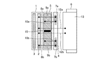
- FIG. 1 is a configuration diagram of an amplifier according to the present embodiment.
- FIG. 2 is a cross-sectional view of the amplifier according to the present embodiment as seen from the horizontal direction.
- the amplifier includes a transistor chip 1, a drain terminal 2, a gate terminal 3, a first substrate 4, a second substrate 5, an output terminal substrate 6, first metal patterns 7a and 7b, and a first metal.
- An isolation resistor 15 is provided.
- the transistor chip 1 is a chip for configuring a transistor such as an FET (Field Effect Transistor).
- the drain terminal 2 and the gate terminal 3 are terminals provided on the surface of the transistor chip 1.
- the first substrate 4 is a substrate having a set relative dielectric constant, and the first metal patterns 7a and 7b and the third metal pattern 11 are provided on the surface thereof.
- the second substrate 5 is a substrate having a relative dielectric constant larger than that of the first substrate 4, and second metal patterns 9a and 9b are provided on the surface thereof.
- the output terminal board 6 is a board for forming an output terminal as an amplifier, and the output terminal 13 is provided on the surface thereof.
- the first metal wires 8a and 8b are metal wires that connect the drain terminal 2 and the first metal patterns 7a and 7b.
- the second metal wires 10a and 10b are metal wires that connect the first metal patterns 7a and 7b and the second metal patterns 9a and 9b.
- the third metal wires 12 a and 12 b are metal wires that connect the drain terminal 2 and the third metal pattern 11.
- the fourth metal wire 14 is a metal wire that connects the third metal pattern 11 and the output terminal 13.
- the isolation resistor 15 is a resistor connected between the second metal patterns 9a and 9b. The isolation resistor 15 is not an essential configuration as an amplifier.
- FIG. 3 is an equivalent circuit diagram of the amplifier according to the first embodiment.
- the equivalent circuit includes an amplifier transistor chip 1, a drain terminal 2, a gate terminal 3, an output terminal 13, inductors 20, 22, 24 and 25, and capacitors 21 and 23.
- the first metal wires 8a and 8b in FIG. the second metal wires 10 a and 10 b are integrated into the inductor 22.
- the third metal wires 12 a and 12 b are integrated into the inductor 24, and the fourth metal wire 14 is integrated into the inductor 25.
- the capacitor 21 is a capacitance between the first metal patterns 7a and 7b via the first substrate 4 and the ground
- the capacitor 23 is the second metal patterns 9a and 9b via the second substrate 5. And ground capacity.
- FIG. 4 is an explanatory diagram showing the frequency dependence of the circuit inductance characteristics as seen from the drain terminal 2 in the amplifier of the first embodiment in comparison with the conventional structure, where the horizontal axis is frequency and the vertical axis is inductance ( Inductance).
- the characteristic 101 is the conventional structure
- the characteristic 102 is the structure of the first embodiment.
- the circuit inductance viewed from the drain terminal 2 tends to increase as the frequency becomes higher, and there is a self-resonance point of the circuit at a certain frequency, and the inductance rapidly increases and has an infinite value.
- the inductance value is not necessarily the value shown in FIG. There may be a plurality of self-resonance points.
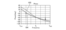
- FIG. 5 is an explanatory diagram showing the frequency dependence of the pass phase characteristics between the drain terminal 2 and the output terminal 13 in the amplifier of the first embodiment in comparison with the conventional structure, where the horizontal axis is the frequency and the vertical axis. Indicates the phase.
- the characteristic 103 is the conventional structure, and the characteristic 104 is the structure of the first embodiment.
- the pass phase characteristic from the drain terminal 2 to the output terminal 13 has a relatively flat frequency characteristic over a certain frequency range. This pass phase characteristic may be only for a desired operating frequency.
- the signal output from the drain terminal 2 is largely divided into two signals: a signal flowing through the third metal wires 12a and 12b and a signal flowing through the first metal wires 8a and 8b.
- a signal flowing through the third metal wires 12 a and 12 b is an output signal path that is finally connected to the output terminal 13 via the third metal pattern 11 and the fourth metal wire 14.
- the third metal wires 12a and 12b, the third metal pattern 11, and the fourth metal wire 14 constitute an output circuit.
- the signals flowing through the first metal wires 8a and 8b are finally transmitted through the first metal patterns 7a and 7b and the second metal wires 10a and 10b on the first substrate 4 and finally on the second substrate 5.
- the two metal patterns 9a and 9b are connected.
- This signal path constitutes an inductor in parallel with the output signal path. This parallel inductor reduces the influence of the transistor parasitic capacitance and can realize a wide band operation.
- FIG. 4 in the configuration of the present embodiment, an unnecessary increase in circuit inductance is reduced for a certain frequency range.
- the center of the frequency axis is the center frequency (f 0 ) (the low frequency region is f Low and the high frequency region f High )
- the self-resonance frequency (Self Resonance) is low in the conventional structure and abruptly near the center frequency
- the inductance has increased.
- wide-band operation is difficult because the impedance of the circuit changes suddenly in the desired band.
- higher self-resonant frequency a low inductance over a wide band at f 0 near. That is, a wide-band amplification operation can be realized without a rapid impedance fluctuation of the circuit.
- the frequency characteristic of the passing phase has less phase fluctuation with respect to f 0 than the conventional structure in a certain frequency range. That is, the frequency dependence of the output circuit is small, and a wideband amplification operation can be realized.
- the first metal patterns 7a and 7b on the first substrate 4 are independent and have a small area. Therefore, the capacitance generated between the back surface of the first substrate 4 and the ground is small, and in the circuit constituting the parallel inductor, the pattern is almost invisible (no influence). That is, in a circuit configuration that requires a parallel inductor, there is an effect of narrowing the operating frequency band because a capacitor is unnecessary, but in the configuration of the present embodiment, the capacitor 21 is connected in FIG. This is equivalent to a circuit that does not, and an ideal parallel inductor composed of inductors 20 and 22 and a capacitor 23 can be realized, and a wideband amplification operation can be realized.
- wires in which signals flow in the same direction are brought close to each other, they interfere with each other and the number of inductors theoretically increases with frequency. Therefore, in this embodiment, wires are intentionally connected in the opposite direction to prevent interference and flatten the operation with respect to the frequency.
- the first embodiment has a configuration using a plurality of substrates. Therefore, if the second metal patterns 9a and 9b are to be capacitive, a substrate having a small relative thickness and a high relative dielectric constant is used. Thereby, the capacitance generated between the pattern and the ground can be increased. Similarly, if it is desired to reduce the capacitance of the first metal patterns 7a and 7b, the thickness of the substrate is increased and a substrate having a small relative dielectric constant is used. A configuration in which the substrate thickness is the same and the relative permittivity is different is also possible. Similarly, a configuration in which the relative dielectric constant is the same and the substrate thickness is different is also possible. In this way, an arbitrary circuit impedance can be realized by combining the substrate thickness and the relative dielectric constant, and a wideband amplification operation can be realized.
- a parallel inductor is configured with the first metal pattern and the second metal wire connecting the first metal pattern and the second metal pattern provided on the second substrate having a relative dielectric constant higher than that of the first substrate.
- the second metal wire is positioned between the first metal wire and the third metal wire, and the direction of the current of the second metal wire is changed to the first metal wire. Is opposite to the current direction of the third metal wire Since the direction, it is possible to amplify the signal to a wide band.
- FIG. FIG. 6 is a configuration diagram of the amplifier according to the second embodiment.
- the amplifier of the second embodiment has a configuration in which a plurality of configurations of the first embodiment are continuously provided, and the configuration of FIG. 6 is an example in which four configurations are provided.
- a common drain terminal 202 and gate terminal 203 are provided in each of the transistor chips 201-1 to 201-4.
- the first substrate 204 and the second substrate 205 are provided in common for the four transistor chips 201-1 to 201-4, and the third metal pattern 211 on the first substrate 204 is also shared. Is provided.
- the output terminal substrate 206 and the output terminal 213 are also provided in common for the transistor chips 201-1 to 201-4.
- the first metal patterns 207a and 207b, the first metal wires 208a and 208b, the second metal patterns 209a and 209b, the second metal wires 210a and 210b, and the third metal wires 212a and 212b are each four. There are pieces. About each structure and operation
- four transistor chips 201-1 to 201-4 are provided as a plurality of multi-transistor chips 201. However, the number is not limited to four and any number is possible. It can be applied to a plurality of values.
- a plurality of transistors are continuously provided, and a plurality of parallel inductors and output circuits are provided corresponding to the plurality of transistors, and the first substrate and the first substrate Since the two substrates are common to the plurality of parallel inductors and the plurality of output circuits, there is an effect that the two substrates can be applied to a plurality of transistor chips.
- FIG. 7 is a configuration diagram of the amplifier according to the third embodiment.
- the amplifier of the third embodiment is obtained by connecting the first metal patterns 7a and 7b with an isolation resistor 16 in the configuration of the first embodiment.
- the other configuration is the same as the configuration shown in FIG. 1, and therefore, the same reference numerals are given to corresponding portions and the description thereof is omitted.
- the basic operation is the same as that of the first embodiment.
- the first metal pattern is a pair of metal patterns composed of two metal patterns, and the pair of metal patterns are connected by an isolation resistor. Therefore, the risk of oscillation can be suppressed. That is, when there is no isolation resistance, unnecessary signals may be generated between the circuits due to the coupling of the metal wires, and oscillation may occur, but in Embodiment 3, the generation of such unnecessary signals is suppressed by the isolation resistance. In addition, oscillation can be suppressed.
- FIG. FIG. 8 is a configuration diagram of the amplifier according to the fourth embodiment.
- the third metal pattern 11 in the configuration of the first embodiment is eliminated, and the third metal wires 12a and 12b are directly connected to the output terminal 13.
- the other configuration is the same as the configuration shown in FIG. 1, and therefore, the same reference numerals are given to corresponding portions and the description thereof is omitted.
- the basic operation is the same as that of the first embodiment.
- the first metal patterns 7a and 7b may be connected by the isolation resistor 16 as in the third embodiment.
- the first metal wire that connects the drain terminal of the transistor and the first metal pattern on the first substrate having the set dielectric constant A parallel inductor is constituted by a first metal pattern and a second metal wire connecting the second metal pattern provided on the second substrate having a relative dielectric constant higher than that of the first substrate, and a transistor
- An output circuit is configured by a third metal wire connecting the drain terminal and the output terminal of the first metal wire, the second metal wire is located between the first metal wire and the third metal wire, and Since the current direction of the second metal wire is opposite to the current direction of the first metal wire and the third metal wire, the size of the substrate and the number of metal wires can be reduced. , Low cost and space saving amplification It can be constructed.
- FIG. 9 is a configuration diagram of the amplifier according to the fifth embodiment.
- the first substrate 4 in the configuration of the first embodiment is separated from the first substrates 4a, 41b and the third metal pattern 11 by the independent substrates 41a, 41b and The substrate 42 is used, and the second substrate 5 in the first embodiment is an independent substrate 51a, 51b for each of the second metal patterns 9a, 9b.
- the isolation resistor 15 in the first embodiment is omitted.
- the other configuration is the same as the configuration shown in FIG. 1, and therefore, the same reference numerals are given to corresponding portions and the description thereof is omitted.
- the basic operation is the same as that of the first embodiment.
- each of the first metal pattern and the second metal pattern is a pair of metal patterns composed of two metal patterns. Since the substrate on which the third metal pattern is installed is an independent substrate, the degree of freedom in the arrangement of the substrate and the arrangement of the metal pattern installed on the substrate can be increased. Impedance and a desired arrangement structure can be easily realized.
- the amplifier according to the present invention relates to a configuration in which a resonance circuit is formed by a wire and a capacitor connected to the drain terminal in the vicinity of the transistor, and is used for a configuration for reducing the parasitic capacitance of the transistor. Suitable for
Landscapes
- Engineering & Computer Science (AREA)
- Power Engineering (AREA)
- Microelectronics & Electronic Packaging (AREA)
- Amplifiers (AREA)
Abstract
ドレイン端子(2)と第1の金属パターン(7a,7b)とを接続する第1の金属ワイヤ(8a,8b)と、第1の金属パターン(7a,7b)と第2の金属パターン(9a,9b)とを接続する第2の金属ワイヤ(10a,10b)とで並列インダクタを構成する。第2の金属ワイヤ(10a,10b)は、第1の金属ワイヤ(8a,8b)と、ドレイン端子(2)と第3の金属パターン(11)とを接続する第3の金属ワイヤ(12a,12b)との間に位置する。第2の金属ワイヤ(10a,10b)の電流の向きを、第1の金属ワイヤ(8a,8b)と第3の金属ワイヤ(12a,12b)の電流の向きとは逆方向とする。
Description
本発明は、トランジスタの出力回路に寄生容量を低減するための金属ワイヤとコンデンサからなる並列インダクタを備えた増幅器に関するものである。
近年、増幅器の広帯域化のために、トランジスタの近傍でドレイン端子に接続された金属ワイヤとコンデンサで共振回路としての並列インダクタを形成する構成が普及している(例えば、特許文献1参照)。共振回路はトランジスタの寄生容量(ドレイン-ソース間の寄生容量Cds)の影響を低減するための回路であり、金属ワイヤ(インダクタ)と回路基板が有するパターン(コンデンサ)とで形成されている。
しかしながら、上記従来の構成では、容量の大きなコンデンサと金属ワイヤのインダクタで整合する回路であるため、コンデンサの容量性が大きく理想的な並列インダクタが実現できず、不要な共振が発生し易いという問題があった。また、並列に設置された金属ワイヤの間には同方向に信号(電流)が流れることから、これら金属ワイヤ間で相互インダクタンスが発生し、トランジスタからみた回路のインダクタンスが大きくなり、所望の回路インピーダンスを実現することができないという問題もあった。このようなことから、従来の構成では、所望帯域の通過特性が狭帯域になり、広帯域に信号を増幅することが困難であるという問題があった。
この発明は、かかる問題を解決するためになされたもので、広帯域に信号を増幅できる増幅器を提供することを目的とする。
この発明に係る増幅器は、トランジスタのドレイン端子と、設定された比誘電率を持つ第1の基板上に設けられた第1の金属パターンとを接続する第1の金属ワイヤと、第1の金属パターンと第1の基板より比誘電率の高い第2の基板上に設けられた第2の金属パターンとを接続する第2の金属ワイヤとで並列インダクタを構成し、トランジスタのドレイン端子と第1の基板上に設けられた第3の金属パターンとを接続する第3の金属ワイヤと、第3の金属パターンと出力端子とを接続する第4の金属ワイヤとで出力回路を構成し、第2の金属ワイヤが、第1の金属ワイヤと第3の金属ワイヤとの間に位置し、かつ、第2の金属ワイヤの電流の向きを、第1の金属ワイヤと第3の金属ワイヤの電流の向きとは逆方向としたものである。
この発明に係る増幅器は、ドレイン端子と第1の金属パターンとを接続する第1の金属ワイヤと、第1の金属パターンと第2の金属パターンとを接続する第2の金属ワイヤとで並列インダクタを構成し、第2の金属ワイヤが、第1の金属ワイヤと、ドレイン端子と第3の金属パターンとを接続する第3の金属ワイヤとの間に位置し、かつ、第2の金属ワイヤの電流の向きを、第1の金属ワイヤと第3の金属ワイヤの電流の向きとは逆方向としたものである。これにより、広帯域に信号を増幅することができる。
以下、この発明をより詳細に説明するために、この発明を実施するための形態について、添付の図面に従って説明する。
実施の形態1.
図1は、本実施の形態による増幅器の構成図である。また、図2は本実施の形態による増幅器を水平方向から見た断面図である。
これらの図において、増幅器は、トランジスタチップ1、ドレイン端子2、ゲート端子3、第1の基板4、第2の基板5、出力端子基板6、第1の金属パターン7a,7b、第1の金属ワイヤ8a,8b、第2の金属パターン9a,9b、第2の金属ワイヤ10a,10b、第3の金属パターン11、第3の金属ワイヤ12a,12b、出力端子13、第4の金属ワイヤ14、アイソレーション抵抗15を備えている。
実施の形態1.
図1は、本実施の形態による増幅器の構成図である。また、図2は本実施の形態による増幅器を水平方向から見た断面図である。
これらの図において、増幅器は、トランジスタチップ1、ドレイン端子2、ゲート端子3、第1の基板4、第2の基板5、出力端子基板6、第1の金属パターン7a,7b、第1の金属ワイヤ8a,8b、第2の金属パターン9a,9b、第2の金属ワイヤ10a,10b、第3の金属パターン11、第3の金属ワイヤ12a,12b、出力端子13、第4の金属ワイヤ14、アイソレーション抵抗15を備えている。
トランジスタチップ1は、例えばFET(Field Effect Transistor)といったトランジスタを構成するためのチップである。ドレイン端子2及びゲート端子3は、トランジスタチップ1の表面上に設けられた端子である。第1の基板4は設定された比誘電率を持つ基板であり、その表面上に第1の金属パターン7a,7bと第3の金属パターン11とが設けられている。第2の基板5は、第1の基板4より比誘電率が大きい基板であり、その表面上に第2の金属パターン9a,9bが設けられている。出力端子基板6は、増幅器としての出力端子を形成するための基板であり、その表面上に出力端子13が設けられている。第1の金属ワイヤ8a,8bは、ドレイン端子2と第1の金属パターン7a,7bとを接続する金属ワイヤである。第2の金属ワイヤ10a,10bは、第1の金属パターン7a,7bと第2の金属パターン9a,9bとを接続する金属ワイヤである。第3の金属ワイヤ12a,12bは、ドレイン端子2と第3の金属パターン11とを接続する金属ワイヤである。第4の金属ワイヤ14は第3の金属パターン11と出力端子13とを接続する金属ワイヤである。アイソレーション抵抗15は、第2の金属パターン9a,9b間に接続された抵抗である。なお、アイソレーション抵抗15は、増幅器として必須の構成ではない。
図3は、実施の形態1における増幅器の等価回路図である。等価回路は、増幅器のトランジスタチップ1、ドレイン端子2、ゲート端子3、出力端子13、インダクタ20、22、24、25、キャパシタ21、23で構成される。ここでは回路を簡略化するために、図1における第1の金属ワイヤ8a,8bをインダクタ20に統合する。また、第2の金属ワイヤ10a,10bをインダクタ22に統合する。さらに、第3の金属ワイヤ12a,12bをインダクタ24に統合し、第4の金属ワイヤ14をインダクタ25に統合している。また、キャパシタ21は、第1の基板4を介した第1の金属パターン7a,7bとグラウンドとの容量であり、キャパシタ23は、第2の基板5を介した第2の金属パターン9a,9bとグラウンドとの容量である。
図4は、実施の形態1の増幅器におけるドレイン端子2から見た回路インダクタンス特性の周波数依存性を従来構造と比較して示す説明図であり、横軸が周波数(Frequency)、縦軸がインダクタンス(Inductance)を示している。また、特性101が従来構造、特性102が実施の形態1の構造である。ドレイン端子2からみた回路インダクタンスは周波数が高くなるにつれて、上昇していく傾向があり、ある周波数で回路の自己共振点が存在し、インダクタンスは急激に上昇し無限大の値を有する。インダクタンスの値は図4に示す値でなくとも、同様の傾向があればよい。また自己共振点は複数存在してもよい。
図5は、実施の形態1の増幅器におけるドレイン端子2と出力端子13間の通過位相特性の周波数依存性を従来構造と比較して示す説明図であり、横軸が周波数(Frequency)、縦軸が位相(Phase)を示している。また、特性103が従来構造、特性104が実施の形態1の構造である。ドレイン端子2から出力端子13の通過位相特性はある周波数範囲に対して比較的平坦な周波数特性を有する。この通過位相特性は所望の動作周波数に対してのみでもよい。
次に、実施の形態1の増幅器の動作原理について説明する。
ドレイン端子2から出る信号は、第3の金属ワイヤ12a,12bに流れる信号と第1の金属ワイヤ8a,8bに流れる信号の二つに大きく分別される。
第3の金属ワイヤ12a,12bに流れる信号は、第3の金属パターン11、第4の金属ワイヤ14を経由して最終的に出力端子13に接続される出力信号経路である。なお、第3の金属ワイヤ12a,12bと、第3の金属パターン11と、第4の金属ワイヤ14とで出力回路を構成している。
ドレイン端子2から出る信号は、第3の金属ワイヤ12a,12bに流れる信号と第1の金属ワイヤ8a,8bに流れる信号の二つに大きく分別される。
第3の金属ワイヤ12a,12bに流れる信号は、第3の金属パターン11、第4の金属ワイヤ14を経由して最終的に出力端子13に接続される出力信号経路である。なお、第3の金属ワイヤ12a,12bと、第3の金属パターン11と、第4の金属ワイヤ14とで出力回路を構成している。
第1の金属ワイヤ8a,8bに流れる信号は、第1の基板4の第1の金属パターン7a,7b、第2の金属ワイヤ10a,10bを経由して最終的に第2の基板5の第2の金属パターン9a,9bに接続される。この信号経路により、出力信号経路に対して並列のインダクタを構成することとなる。この並列インダクタがトランジスタ寄生容量の影響を低減し、広帯域動作が実現できる。
次に、実施の形態1の増幅器によって得られる特性を説明する。
図4に示すように、本実施の形態の構成では、ある周波数範囲に対して回路のインダクタンスの不要増加を低減している。図4において、周波数軸の中心を中心周波数(f0)とすると(低周波領域をfLow、高周波数領域fHigh)、従来構造では自己共振周波数(Self Resonance)が低く、中心周波数近傍で急激にインダクタンスが増加している。つまり所望帯域で回路のインピーダンスが急変することで広帯域動作が困難である。本実施の形態では自己共振周波数が高く、f0近傍で広い帯域にわたって低インダクタンスである。つまり回路の急激なインピーダンス変動が無く広帯域な増幅動作を実現できる。
図4に示すように、本実施の形態の構成では、ある周波数範囲に対して回路のインダクタンスの不要増加を低減している。図4において、周波数軸の中心を中心周波数(f0)とすると(低周波領域をfLow、高周波数領域fHigh)、従来構造では自己共振周波数(Self Resonance)が低く、中心周波数近傍で急激にインダクタンスが増加している。つまり所望帯域で回路のインピーダンスが急変することで広帯域動作が困難である。本実施の形態では自己共振周波数が高く、f0近傍で広い帯域にわたって低インダクタンスである。つまり回路の急激なインピーダンス変動が無く広帯域な増幅動作を実現できる。
図5に示すように、本実施の形態の構成ではある周波数範囲に対して、通過位相の周波数特性が従来構造よりもf0に対しての位相変動が少ない。つまり出力回路の周波数依存性が小さく、広帯域な増幅動作が実現できる。
次に、図4及び図5に示す特性が得られる原理を説明する。
図1に示すように、本実施の形態では第1の基板4にある第1の金属パターン7a,7bはそれぞれが独立し、かつ面積が小さい。そのため第1の基板4裏面のグランドとの間に発生する容量が小さく、並列のインダクタを構成する回路において、ほぼ容量性が見えない(影響がない)パターンである。すなわち、並列インダクタを必要としている回路構成において、容量は不要な存在であるので動作する周波数帯域を狭めてしまう影響があるが、本実施の形態の構成は、図3において、キャパシタ21が接続されていない回路と同等となり、インダクタ20、22、キャパシタ23から成る理想的な並列インダクタが実現でき広帯域な増幅動作が実現できる。
図1に示すように、本実施の形態では第1の基板4にある第1の金属パターン7a,7bはそれぞれが独立し、かつ面積が小さい。そのため第1の基板4裏面のグランドとの間に発生する容量が小さく、並列のインダクタを構成する回路において、ほぼ容量性が見えない(影響がない)パターンである。すなわち、並列インダクタを必要としている回路構成において、容量は不要な存在であるので動作する周波数帯域を狭めてしまう影響があるが、本実施の形態の構成は、図3において、キャパシタ21が接続されていない回路と同等となり、インダクタ20、22、キャパシタ23から成る理想的な並列インダクタが実現でき広帯域な増幅動作が実現できる。
第2の金属ワイヤ10a,10bは、出力信号経路である第3の金属ワイヤ12a,12b及び第1の金属ワイヤ8a,8bに対して逆方向の信号(電流)が流れる。このように逆向きに折り返すように打たれた金属ワイヤがあることで、出力信号経路である第3の金属ワイヤ12a,12b及び第1の金属ワイヤ8a,8b間に発生する相互インダクタンス(不要干渉)を低減することができ、広帯域な増幅動作が実現できる。従来構造では相互インダクタンスを低減する構造ではないので回路のインダクタンスが増加してしまう。すなわち、従来構造のように、同方向に信号が流れるワイヤ(線路)を近接させると、互いが不要干渉し理論上インダクタが周波数に応じて増加する。そのために、本実施の形態ではあえて逆方向にワイヤを接続し、干渉を防ぎ、周波数に対する動作を平坦にしている。
また、図1及び図2に示すように、実施の形態1は複数の基板を用いた構成である。そのため、第2の金属パターン9a,9bに容量性を持たせたいのであれば、基板厚みを薄くし、比誘電率が大きい基板を用いる。これによりパターンとグランド間に生じる容量を大きくすることができる。同様に、第1の金属パターン7a,7bの容量性を小さくしたいのであれば、基板の厚みを厚くし、比誘電率が小さい基板を用いる。基板厚みは同じで比誘電率が異なる構成も可能である。同様に比誘電率は同じで基板厚みが異なる構成も可能である。このように基板厚みと比誘電率を組み合わせることで任意の回路インピーダンスを実現でき、広帯域な増幅動作が実現できる。
以上説明したように、実施の形態1の増幅器によれば、トランジスタのドレイン端子と、設定された比誘電率を持つ第1の基板上に設けられた第1の金属パターンとを接続する第1の金属ワイヤと、第1の金属パターンと第1の基板より比誘電率の高い第2の基板上に設けられた第2の金属パターンとを接続する第2の金属ワイヤとで並列インダクタを構成し、トランジスタのドレイン端子と第1の基板上に設けられた第3の金属パターンとを接続する第3の金属ワイヤと、第3の金属パターンと出力端子とを接続する第4の金属ワイヤとで出力回路を構成し、第2の金属ワイヤが、第1の金属ワイヤと第3の金属ワイヤとの間に位置し、かつ、第2の金属ワイヤの電流の向きを、第1の金属ワイヤと第3の金属ワイヤの電流の向きとは逆方向としたので、広帯域に信号を増幅することができる。
実施の形態2.
図6は、実施の形態2の増幅器の構成図である。
実施の形態2の増幅器は、実施の形態1の構成を複数個連続して設けたものであり、図6の構成は4個分設けた例である。図示のように、4個分のマルチトランジスタチップ201では、各トランジスタチップ201-1~201-4で共通のドレイン端子202とゲート端子203が設けられている。また、四つのトランジスタチップ201-1~201-4に対して、第1の基板204と第2の基板205は共通に設けられ、第1の基板204上の第3の金属パターン211も共通に設けられている。さらに、出力端子基板206及び出力端子213もトランジスタチップ201-1~201-4に対して共通に設けられている。一方、第1の金属パターン207a,207b、第1の金属ワイヤ208a,208b、第2の金属パターン209a,209b、第2の金属ワイヤ210a,210b、第3の金属ワイヤ212a,212bは、それぞれ4個分が設けられている。それぞれの構成及び動作については、実施の形態1の構成が4個分設けられているのと同様であるため、ここでの説明は省略する。
なお、上記例では複数のマルチトランジスタチップ201として、4個分のトランジスタチップ201-1~201-4が設けられている例を説明したが、個数は4個に限定されるものではなく、任意の複数の値に対して適用が可能である。
図6は、実施の形態2の増幅器の構成図である。
実施の形態2の増幅器は、実施の形態1の構成を複数個連続して設けたものであり、図6の構成は4個分設けた例である。図示のように、4個分のマルチトランジスタチップ201では、各トランジスタチップ201-1~201-4で共通のドレイン端子202とゲート端子203が設けられている。また、四つのトランジスタチップ201-1~201-4に対して、第1の基板204と第2の基板205は共通に設けられ、第1の基板204上の第3の金属パターン211も共通に設けられている。さらに、出力端子基板206及び出力端子213もトランジスタチップ201-1~201-4に対して共通に設けられている。一方、第1の金属パターン207a,207b、第1の金属ワイヤ208a,208b、第2の金属パターン209a,209b、第2の金属ワイヤ210a,210b、第3の金属ワイヤ212a,212bは、それぞれ4個分が設けられている。それぞれの構成及び動作については、実施の形態1の構成が4個分設けられているのと同様であるため、ここでの説明は省略する。
なお、上記例では複数のマルチトランジスタチップ201として、4個分のトランジスタチップ201-1~201-4が設けられている例を説明したが、個数は4個に限定されるものではなく、任意の複数の値に対して適用が可能である。
以上説明したように、実施の形態2の増幅器によれば、トランジスタを複数連続して設け、かつ、並列インダクタと出力回路とを複数のトランジスタに対応して複数設けると共に、第1の基板及び第2の基板を、複数の並列インダクタ及び複数の出力回路において共通としたので、複数のトランジスタチップに適用できるという効果がある。
実施の形態3.
図7は、実施の形態3の増幅器の構成図である。
実施の形態3の増幅器は、実施の形態1の構成において、第1の金属パターン7a,7b間をアイソレーション抵抗16で接続したものである。他の構成については、図1で示した構成と同様であるため、対応する部分に同一符号を付してその説明を省略する。また、基本的な動作については実施の形態1と同様である。
図7は、実施の形態3の増幅器の構成図である。
実施の形態3の増幅器は、実施の形態1の構成において、第1の金属パターン7a,7b間をアイソレーション抵抗16で接続したものである。他の構成については、図1で示した構成と同様であるため、対応する部分に同一符号を付してその説明を省略する。また、基本的な動作については実施の形態1と同様である。
以上説明したように、実施の形態3の増幅器によれば、第1の金属パターンは、二つの金属パターンからなる一対の金属パターンであり、かつ、一対の金属パターン間をアイソレーション抵抗で接続したので、発振の恐れを抑制することができる。すなわち、アイソレーション抵抗が無い場合は金属ワイヤの結合で不要信号が回路間に発生して発振する恐れがあるが、実施の形態3ではアイソレーション抵抗によって、このような不要な信号の発生を抑制し、発振を抑制することができる。
実施の形態4.
図8は、実施の形態4の増幅器の構成図である。
実施の形態4の増幅器は、実施の形態1の構成における第3の金属パターン11を無くし、第3の金属ワイヤ12a,12bを直接出力端子13に接続するようにしたものである。他の構成については、図1で示した構成と同様であるため、対応する部分に同一符号を付してその説明を省略する。また、基本的な動作については実施の形態1と同様である。なお、実施の形態4においても、実施の形態3と同様に、第1の金属パターン7a,7b間をアイソレーション抵抗16で接続してもよい。
図8は、実施の形態4の増幅器の構成図である。
実施の形態4の増幅器は、実施の形態1の構成における第3の金属パターン11を無くし、第3の金属ワイヤ12a,12bを直接出力端子13に接続するようにしたものである。他の構成については、図1で示した構成と同様であるため、対応する部分に同一符号を付してその説明を省略する。また、基本的な動作については実施の形態1と同様である。なお、実施の形態4においても、実施の形態3と同様に、第1の金属パターン7a,7b間をアイソレーション抵抗16で接続してもよい。
以上説明したように、実施の形態4の増幅器によれば、トランジスタのドレイン端子と設定された比誘電率を持つ第1の基板上の第1の金属パターンとを接続する第1の金属ワイヤと、第1の金属パターンと第1の基板より比誘電率の高い第2の基板上に設けられた第2の金属パターンとを接続する第2の金属ワイヤとで、並列インダクタを構成し、トランジスタのドレイン端子と出力端子とを接続する第3の金属ワイヤで出力回路を構成し、第2の金属ワイヤが、第1の金属ワイヤと第3の金属ワイヤとの間に位置し、かつ、第2の金属ワイヤの電流の向きを、第1の金属ワイヤと第3の金属ワイヤの電流の向きとは逆方向としたので、基板の大きさや金属ワイヤの本数を削減することができ、その結果、低コスト及び省スペースで増幅器を構成することができる。
実施の形態5.
図9は、実施の形態5の増幅器の構成図である。
実施の形態5の増幅器は、実施の形態1の構成における第1の基板4を、第1の金属パターン7a,7bと第3の金属パターン11の設置部毎に、独立した基板41a,41b及び基板42とし、また、実施の形態1における第2の基板5を第2の金属パターン9a,9b毎に独立した基板51a,51bとしたものである。なお、実施の形態5では、実施の形態1におけるアイソレーション抵抗15は削除されている。他の構成については、図1で示した構成と同様であるため、対応する部分に同一符号を付してその説明を省略する。また、基本的な動作については実施の形態1と同様である。
図9は、実施の形態5の増幅器の構成図である。
実施の形態5の増幅器は、実施の形態1の構成における第1の基板4を、第1の金属パターン7a,7bと第3の金属パターン11の設置部毎に、独立した基板41a,41b及び基板42とし、また、実施の形態1における第2の基板5を第2の金属パターン9a,9b毎に独立した基板51a,51bとしたものである。なお、実施の形態5では、実施の形態1におけるアイソレーション抵抗15は削除されている。他の構成については、図1で示した構成と同様であるため、対応する部分に同一符号を付してその説明を省略する。また、基本的な動作については実施の形態1と同様である。
以上説明したように、実施の形態5の増幅器によれば、第1の金属パターン及び第2の金属パターンは、それぞれ、二つの金属パターンからなる一対の金属パターンであり、これら一対の金属パターン及び第3の金属パターンが設置される基板をそれぞれ独立した基板としたので、基板の配置や、基板上に設置される金属パターンの配置の自由度を高くすることができ、従って、増幅器としての所望のインピーダンスや所望の配置構造を容易に実現することができる。
なお、本願発明はその発明の範囲内において、各実施の形態の自由な組み合わせ、あるいは各実施の形態の任意の構成要素の変形、もしくは各実施の形態において任意の構成要素の省略が可能である。
以上のように、この発明に係る増幅器は、トランジスタの近傍でドレイン端子に接続されたワイヤとコンデンサで共振回路を形成する構成に関するものであり、トランジスタの寄生容量を低減するための構成に用いるのに適している。
1,201-1~201-4 トランジスタチップ、2,202 ドレイン端子、3,203 ゲート端子、4,204 第1の基板、5,205 第2の基板、6,206 出力端子基板、7a,7b,207a,207b 第1の金属パターン、8a,8b,208a,208b 第1の金属ワイヤ、9a,9b,209a,209b 第2の金属パターン、10a,10b,210a,210b 第2の金属ワイヤ、11,211 第3の金属パターン、12a,12b,212a,212b 第3の金属ワイヤ、13,213 出力端子、14,214 第4の金属ワイヤ、15,16 アイソレーション抵抗、41a,41b,42 51a,51b 基板、201 マルチトランジスタチップ。
Claims (5)
- トランジスタのドレイン端子と、設定された比誘電率を持つ第1の基板上に設けられた第1の金属パターンとを接続する第1の金属ワイヤと、前記第1の金属パターンと前記第1の基板より比誘電率の高い第2の基板上に設けられた第2の金属パターンとを接続する第2の金属ワイヤとで並列インダクタを構成し、
前記トランジスタのドレイン端子と前記第1の基板上に設けられた第3の金属パターンとを接続する第3の金属ワイヤと、前記第3の金属パターンと出力端子とを接続する第4の金属ワイヤとで出力回路を構成し、
前記第2の金属ワイヤが、前記第1の金属ワイヤと前記第3の金属ワイヤとの間に位置し、かつ、前記第2の金属ワイヤの電流の向きを、前記第1の金属ワイヤと前記第3の金属ワイヤの電流の向きとは逆方向としたことを特徴とする増幅器。 - 前記トランジスタを複数連続して設け、かつ、前記並列インダクタと前記出力回路とを前記複数のトランジスタに対応して複数設けると共に、前記第1の基板及び前記第2の基板を、前記複数の並列インダクタ及び前記複数の出力回路において共通としたことを特徴とする請求項1記載の増幅器。
- 前記第1の金属パターンは、二つの金属パターンからなる一対の金属パターンであり、かつ、当該一対の金属パターン間をアイソレーション抵抗で接続したことを特徴とする請求項1記載の増幅器。
- トランジスタのドレイン端子と設定された比誘電率を持つ第1の基板上の第1の金属パターンとを接続する第1の金属ワイヤと、前記第1の金属パターンと前記第1の基板より比誘電率の高い第2の基板上に設けられた第2の金属パターンとを接続する第2の金属ワイヤとで、並列インダクタを構成し、
前記トランジスタのドレイン端子と出力端子とを接続する第3の金属ワイヤで出力回路を構成し、
前記第2の金属ワイヤが、前記第1の金属ワイヤと前記第3の金属ワイヤとの間に位置し、かつ、前記第2の金属ワイヤの電流の向きを、前記第1の金属ワイヤと前記第3の金属ワイヤの電流の向きとは逆方向としたことを特徴とする増幅器。 - 前記第1の金属パターン及び前記第2の金属パターンは、それぞれ、二つの金属パターンからなる一対の金属パターンであり、これら一対の金属パターン及び前記第3の金属パターンが設置される基板をそれぞれ独立した基板としたことを特徴とする請求項1記載の増幅器。
Priority Applications (5)
| Application Number | Priority Date | Filing Date | Title |
|---|---|---|---|
| PCT/JP2016/069620 WO2018003111A1 (ja) | 2016-07-01 | 2016-07-01 | 増幅器 |
| JP2018524701A JP6377305B2 (ja) | 2016-07-01 | 2016-07-01 | 増幅器 |
| EP16907344.2A EP3462608A4 (en) | 2016-07-01 | 2016-07-01 | AMPLIFIER |
| US16/099,968 US10748860B2 (en) | 2016-07-01 | 2016-07-01 | Amplifier |
| CN201680086907.1A CN109417364A (zh) | 2016-07-01 | 2016-07-01 | 放大器 |
Applications Claiming Priority (1)
| Application Number | Priority Date | Filing Date | Title |
|---|---|---|---|
| PCT/JP2016/069620 WO2018003111A1 (ja) | 2016-07-01 | 2016-07-01 | 増幅器 |
Publications (1)
| Publication Number | Publication Date |
|---|---|
| WO2018003111A1 true WO2018003111A1 (ja) | 2018-01-04 |
Family
ID=60787481
Family Applications (1)
| Application Number | Title | Priority Date | Filing Date |
|---|---|---|---|
| PCT/JP2016/069620 Ceased WO2018003111A1 (ja) | 2016-07-01 | 2016-07-01 | 増幅器 |
Country Status (5)
| Country | Link |
|---|---|
| US (1) | US10748860B2 (ja) |
| EP (1) | EP3462608A4 (ja) |
| JP (1) | JP6377305B2 (ja) |
| CN (1) | CN109417364A (ja) |
| WO (1) | WO2018003111A1 (ja) |
Cited By (1)
| Publication number | Priority date | Publication date | Assignee | Title |
|---|---|---|---|---|
| WO2019202631A1 (ja) * | 2018-04-16 | 2019-10-24 | 三菱電機株式会社 | 高周波電力増幅器 |
Citations (4)
| Publication number | Priority date | Publication date | Assignee | Title |
|---|---|---|---|---|
| JPH065794A (ja) * | 1992-06-19 | 1994-01-14 | Hitachi Ltd | 高周波増幅装置 |
| JP2004523172A (ja) * | 2001-02-28 | 2004-07-29 | モトローラ・インコーポレイテッド | インピーダンス整合のための装置及び方法 |
| US7564303B2 (en) | 2005-07-26 | 2009-07-21 | Infineon Technologies Ag | Semiconductor power device and RF signal amplifier |
| JP2013118580A (ja) * | 2011-12-05 | 2013-06-13 | Mitsubishi Electric Corp | 高周波増幅器 |
Family Cites Families (10)
| Publication number | Priority date | Publication date | Assignee | Title |
|---|---|---|---|---|
| US6181200B1 (en) * | 1999-04-09 | 2001-01-30 | Integra Technologies, Inc. | Radio frequency power device |
| JP2005516444A (ja) * | 2002-01-24 | 2005-06-02 | コーニンクレッカ フィリップス エレクトロニクス エヌ ヴィ | 補償されたrf増幅器デバイス |
| US6734728B1 (en) | 2002-12-19 | 2004-05-11 | Infineon Technologies North America Corp. | RF power transistor with internal bias feed |
| US20080246547A1 (en) * | 2005-03-18 | 2008-10-09 | Nxp B.V. | Method And System for Output Matching of Rf Transistors |
| US7372334B2 (en) * | 2005-07-26 | 2008-05-13 | Infineon Technologies Ag | Output match transistor |
| EP2463905B1 (en) * | 2010-12-10 | 2014-10-01 | Nxp B.V. | Packaged RF transistor with special supply voltage leads |
| EP2843691A4 (en) * | 2012-04-27 | 2015-12-02 | Mitsubishi Electric Corp | FIELD-CHIP |
| JP6191016B2 (ja) * | 2012-11-09 | 2017-09-06 | パナソニックIpマネジメント株式会社 | 半導体装置 |
| JP2014138305A (ja) * | 2013-01-17 | 2014-07-28 | Mitsubishi Electric Corp | 高周波電力増幅器 |
| EP2933835A1 (en) * | 2014-04-15 | 2015-10-21 | Nxp B.V. | RF power transistor |
-
2016
- 2016-07-01 EP EP16907344.2A patent/EP3462608A4/en not_active Withdrawn
- 2016-07-01 CN CN201680086907.1A patent/CN109417364A/zh not_active Withdrawn
- 2016-07-01 WO PCT/JP2016/069620 patent/WO2018003111A1/ja not_active Ceased
- 2016-07-01 US US16/099,968 patent/US10748860B2/en active Active
- 2016-07-01 JP JP2018524701A patent/JP6377305B2/ja active Active
Patent Citations (4)
| Publication number | Priority date | Publication date | Assignee | Title |
|---|---|---|---|---|
| JPH065794A (ja) * | 1992-06-19 | 1994-01-14 | Hitachi Ltd | 高周波増幅装置 |
| JP2004523172A (ja) * | 2001-02-28 | 2004-07-29 | モトローラ・インコーポレイテッド | インピーダンス整合のための装置及び方法 |
| US7564303B2 (en) | 2005-07-26 | 2009-07-21 | Infineon Technologies Ag | Semiconductor power device and RF signal amplifier |
| JP2013118580A (ja) * | 2011-12-05 | 2013-06-13 | Mitsubishi Electric Corp | 高周波増幅器 |
Non-Patent Citations (1)
| Title |
|---|
| See also references of EP3462608A4 |
Cited By (2)
| Publication number | Priority date | Publication date | Assignee | Title |
|---|---|---|---|---|
| WO2019202631A1 (ja) * | 2018-04-16 | 2019-10-24 | 三菱電機株式会社 | 高周波電力増幅器 |
| JPWO2019202631A1 (ja) * | 2018-04-16 | 2020-12-17 | 三菱電機株式会社 | 高周波電力増幅器 |
Also Published As
| Publication number | Publication date |
|---|---|
| JP6377305B2 (ja) | 2018-08-22 |
| CN109417364A (zh) | 2019-03-01 |
| EP3462608A4 (en) | 2019-06-19 |
| US20190148315A1 (en) | 2019-05-16 |
| JPWO2018003111A1 (ja) | 2018-08-23 |
| US10748860B2 (en) | 2020-08-18 |
| EP3462608A1 (en) | 2019-04-03 |
Similar Documents
| Publication | Publication Date | Title |
|---|---|---|
| EP3337037B1 (en) | Doherty amplifiers and amplifier modules with shunt inductance circuits that affect transmission line length between carrier and peaking amplifier outputs | |
| US10594266B2 (en) | Multiple-path amplifier with series component along inverter between amplifier outputs | |
| US9082543B2 (en) | Inductor | |
| JP4750106B2 (ja) | 中心タップを備える差動モードインダクタ | |
| JP2004281625A (ja) | 半導体装置 | |
| JP2005311852A (ja) | 高周波増幅装置 | |
| US6822518B1 (en) | Low noise amplifier | |
| KR102163060B1 (ko) | 인덕터 및 인덕터를 포함하는 저잡음 증폭기 | |
| TW201039552A (en) | A low noise cascode amplifier | |
| JP2013191910A (ja) | 増幅器および増幅方法 | |
| KR20220088486A (ko) | 고주파 증폭기 | |
| JP6377305B2 (ja) | 増幅器 | |
| JP2004304330A (ja) | 周波数特性可変増幅回路及び半導体集積回路装置 | |
| JP6407194B2 (ja) | 差動増幅器のための高周波変圧器 | |
| CN100442656C (zh) | 低噪声放大器及放大信号的方法 | |
| JP5862653B2 (ja) | スイッチング回路および高周波モジュール | |
| US8922306B2 (en) | Reduced size bias tee | |
| KR101560522B1 (ko) | 고주파 접지 구조와 전력 증폭기를 가지는 전자 회로 장치 | |
| JP6532618B2 (ja) | 高周波回路及び高周波電力増幅器 | |
| JP2021078103A (ja) | 能動バラン回路、電力増幅回路および電力増幅モジュール | |
| TWI879036B (zh) | 放大器系統和形成高頻放大器電路的方法 | |
| JP2004080826A (ja) | マイクロ波増幅器 | |
| Danson et al. | Design and characterization of a MEMS capacitive switch for improved RF amplifier circuits | |
| CN118199533A (zh) | 放大器系统及其形成方法 | |
| JP4425755B2 (ja) | 差動増幅回路 |
Legal Events
| Date | Code | Title | Description |
|---|---|---|---|
| ENP | Entry into the national phase |
Ref document number: 2018524701 Country of ref document: JP Kind code of ref document: A |
|
| 121 | Ep: the epo has been informed by wipo that ep was designated in this application |
Ref document number: 16907344 Country of ref document: EP Kind code of ref document: A1 |
|
| NENP | Non-entry into the national phase |
Ref country code: DE |
|
| ENP | Entry into the national phase |
Ref document number: 2016907344 Country of ref document: EP Effective date: 20181231 |