WO2018020746A1 - 多孔質の低誘電性ポリマーフィルム及びミリ波アンテナ用フィルム - Google Patents
多孔質の低誘電性ポリマーフィルム及びミリ波アンテナ用フィルム Download PDFInfo
- Publication number
- WO2018020746A1 WO2018020746A1 PCT/JP2017/014375 JP2017014375W WO2018020746A1 WO 2018020746 A1 WO2018020746 A1 WO 2018020746A1 JP 2017014375 W JP2017014375 W JP 2017014375W WO 2018020746 A1 WO2018020746 A1 WO 2018020746A1
- Authority
- WO
- WIPO (PCT)
- Prior art keywords
- film
- film according
- porous
- base material
- polyimide
- Prior art date
- Legal status (The legal status is an assumption and is not a legal conclusion. Google has not performed a legal analysis and makes no representation as to the accuracy of the status listed.)
- Ceased
Links
Images


Classifications
-
- C—CHEMISTRY; METALLURGY
- C08—ORGANIC MACROMOLECULAR COMPOUNDS; THEIR PREPARATION OR CHEMICAL WORKING-UP; COMPOSITIONS BASED THEREON
- C08J—WORKING-UP; GENERAL PROCESSES OF COMPOUNDING; AFTER-TREATMENT NOT COVERED BY SUBCLASSES C08B, C08C, C08F, C08G or C08H
- C08J9/00—Working-up of macromolecular substances to porous or cellular articles or materials; After-treatment thereof
- C08J9/34—Chemical features in the manufacture of articles consisting of a foamed macromolecular core and a macromolecular surface layer having a higher density than the core
-
- B—PERFORMING OPERATIONS; TRANSPORTING
- B32—LAYERED PRODUCTS
- B32B—LAYERED PRODUCTS, i.e. PRODUCTS BUILT-UP OF STRATA OF FLAT OR NON-FLAT, e.g. CELLULAR OR HONEYCOMB, FORM
- B32B27/00—Layered products comprising a layer of synthetic resin
- B32B27/06—Layered products comprising a layer of synthetic resin as the main or only constituent of a layer, which is next to another layer of the same or of a different material
- B32B27/08—Layered products comprising a layer of synthetic resin as the main or only constituent of a layer, which is next to another layer of the same or of a different material of synthetic resin
-
- B—PERFORMING OPERATIONS; TRANSPORTING
- B32—LAYERED PRODUCTS
- B32B—LAYERED PRODUCTS, i.e. PRODUCTS BUILT-UP OF STRATA OF FLAT OR NON-FLAT, e.g. CELLULAR OR HONEYCOMB, FORM
- B32B27/00—Layered products comprising a layer of synthetic resin
- B32B27/28—Layered products comprising a layer of synthetic resin comprising synthetic resins not wholly covered by any one of the sub-groups B32B27/30 - B32B27/42
- B32B27/281—Layered products comprising a layer of synthetic resin comprising synthetic resins not wholly covered by any one of the sub-groups B32B27/30 - B32B27/42 comprising polyimides
-
- B—PERFORMING OPERATIONS; TRANSPORTING
- B32—LAYERED PRODUCTS
- B32B—LAYERED PRODUCTS, i.e. PRODUCTS BUILT-UP OF STRATA OF FLAT OR NON-FLAT, e.g. CELLULAR OR HONEYCOMB, FORM
- B32B7/00—Layered products characterised by the relation between layers; Layered products characterised by the relative orientation of features between layers, or by the relative values of a measurable parameter between layers, i.e. products comprising layers having different physical, chemical or physicochemical properties; Layered products characterised by the interconnection of layers
- B32B7/02—Physical, chemical or physicochemical properties
- B32B7/022—Mechanical properties
-
- B—PERFORMING OPERATIONS; TRANSPORTING
- B32—LAYERED PRODUCTS
- B32B—LAYERED PRODUCTS, i.e. PRODUCTS BUILT-UP OF STRATA OF FLAT OR NON-FLAT, e.g. CELLULAR OR HONEYCOMB, FORM
- B32B7/00—Layered products characterised by the relation between layers; Layered products characterised by the relative orientation of features between layers, or by the relative values of a measurable parameter between layers, i.e. products comprising layers having different physical, chemical or physicochemical properties; Layered products characterised by the interconnection of layers
- B32B7/02—Physical, chemical or physicochemical properties
- B32B7/025—Electric or magnetic properties
-
- C—CHEMISTRY; METALLURGY
- C08—ORGANIC MACROMOLECULAR COMPOUNDS; THEIR PREPARATION OR CHEMICAL WORKING-UP; COMPOSITIONS BASED THEREON
- C08G—MACROMOLECULAR COMPOUNDS OBTAINED OTHERWISE THAN BY REACTIONS ONLY INVOLVING UNSATURATED CARBON-TO-CARBON BONDS
- C08G73/00—Macromolecular compounds obtained by reactions forming a linkage containing nitrogen with or without oxygen or carbon in the main chain of the macromolecule, not provided for in groups C08G12/00 - C08G71/00
- C08G73/06—Polycondensates having nitrogen-containing heterocyclic rings in the main chain of the macromolecule
- C08G73/10—Polyimides; Polyester-imides; Polyamide-imides; Polyamide acids or similar polyimide precursors
- C08G73/1003—Preparatory processes
- C08G73/1007—Preparatory processes from tetracarboxylic acids or derivatives and diamines
-
- C—CHEMISTRY; METALLURGY
- C08—ORGANIC MACROMOLECULAR COMPOUNDS; THEIR PREPARATION OR CHEMICAL WORKING-UP; COMPOSITIONS BASED THEREON
- C08G—MACROMOLECULAR COMPOUNDS OBTAINED OTHERWISE THAN BY REACTIONS ONLY INVOLVING UNSATURATED CARBON-TO-CARBON BONDS
- C08G73/00—Macromolecular compounds obtained by reactions forming a linkage containing nitrogen with or without oxygen or carbon in the main chain of the macromolecule, not provided for in groups C08G12/00 - C08G71/00
- C08G73/06—Polycondensates having nitrogen-containing heterocyclic rings in the main chain of the macromolecule
- C08G73/10—Polyimides; Polyester-imides; Polyamide-imides; Polyamide acids or similar polyimide precursors
- C08G73/1067—Wholly aromatic polyimides, i.e. having both tetracarboxylic and diamino moieties aromatically bound
- C08G73/1071—Wholly aromatic polyimides containing oxygen in the form of ether bonds in the main chain
-
- C—CHEMISTRY; METALLURGY
- C08—ORGANIC MACROMOLECULAR COMPOUNDS; THEIR PREPARATION OR CHEMICAL WORKING-UP; COMPOSITIONS BASED THEREON
- C08J—WORKING-UP; GENERAL PROCESSES OF COMPOUNDING; AFTER-TREATMENT NOT COVERED BY SUBCLASSES C08B, C08C, C08F, C08G or C08H
- C08J5/00—Manufacture of articles or shaped materials containing macromolecular substances
- C08J5/18—Manufacture of films or sheets
-
- C—CHEMISTRY; METALLURGY
- C08—ORGANIC MACROMOLECULAR COMPOUNDS; THEIR PREPARATION OR CHEMICAL WORKING-UP; COMPOSITIONS BASED THEREON
- C08J—WORKING-UP; GENERAL PROCESSES OF COMPOUNDING; AFTER-TREATMENT NOT COVERED BY SUBCLASSES C08B, C08C, C08F, C08G or C08H
- C08J9/00—Working-up of macromolecular substances to porous or cellular articles or materials; After-treatment thereof
- C08J9/26—Working-up of macromolecular substances to porous or cellular articles or materials; After-treatment thereof by elimination of a solid phase from a macromolecular composition or article, e.g. leaching out
-
- H—ELECTRICITY
- H10—SEMICONDUCTOR DEVICES; ELECTRIC SOLID-STATE DEVICES NOT OTHERWISE PROVIDED FOR
- H10W—GENERIC PACKAGES, INTERCONNECTIONS, CONNECTORS OR OTHER CONSTRUCTIONAL DETAILS OF DEVICES COVERED BY CLASS H10
- H10W70/00—Package substrates; Interposers; Redistribution layers [RDL]
- H10W70/60—Insulating or insulated package substrates; Interposers; Redistribution layers
- H10W70/67—Insulating or insulated package substrates; Interposers; Redistribution layers characterised by their insulating layers or insulating parts
- H10W70/69—Insulating materials thereof
- H10W70/695—Organic materials
-
- B—PERFORMING OPERATIONS; TRANSPORTING
- B32—LAYERED PRODUCTS
- B32B—LAYERED PRODUCTS, i.e. PRODUCTS BUILT-UP OF STRATA OF FLAT OR NON-FLAT, e.g. CELLULAR OR HONEYCOMB, FORM
- B32B2250/00—Layers arrangement
- B32B2250/02—2 layers
-
- B—PERFORMING OPERATIONS; TRANSPORTING
- B32—LAYERED PRODUCTS
- B32B—LAYERED PRODUCTS, i.e. PRODUCTS BUILT-UP OF STRATA OF FLAT OR NON-FLAT, e.g. CELLULAR OR HONEYCOMB, FORM
- B32B2305/00—Condition, form or state of the layers or laminate
- B32B2305/02—Cellular or porous
- B32B2305/026—Porous
-
- B—PERFORMING OPERATIONS; TRANSPORTING
- B32—LAYERED PRODUCTS
- B32B—LAYERED PRODUCTS, i.e. PRODUCTS BUILT-UP OF STRATA OF FLAT OR NON-FLAT, e.g. CELLULAR OR HONEYCOMB, FORM
- B32B2307/00—Properties of the layers or laminate
- B32B2307/20—Properties of the layers or laminate having particular electrical or magnetic properties, e.g. piezoelectric
- B32B2307/204—Di-electric
-
- B—PERFORMING OPERATIONS; TRANSPORTING
- B32—LAYERED PRODUCTS
- B32B—LAYERED PRODUCTS, i.e. PRODUCTS BUILT-UP OF STRATA OF FLAT OR NON-FLAT, e.g. CELLULAR OR HONEYCOMB, FORM
- B32B2307/00—Properties of the layers or laminate
- B32B2307/70—Other properties
- B32B2307/726—Permeability to liquids, absorption
- B32B2307/7265—Non-permeable
-
- B—PERFORMING OPERATIONS; TRANSPORTING
- B32—LAYERED PRODUCTS
- B32B—LAYERED PRODUCTS, i.e. PRODUCTS BUILT-UP OF STRATA OF FLAT OR NON-FLAT, e.g. CELLULAR OR HONEYCOMB, FORM
- B32B2307/00—Properties of the layers or laminate
- B32B2307/70—Other properties
- B32B2307/732—Dimensional properties
-
- C—CHEMISTRY; METALLURGY
- C08—ORGANIC MACROMOLECULAR COMPOUNDS; THEIR PREPARATION OR CHEMICAL WORKING-UP; COMPOSITIONS BASED THEREON
- C08J—WORKING-UP; GENERAL PROCESSES OF COMPOUNDING; AFTER-TREATMENT NOT COVERED BY SUBCLASSES C08B, C08C, C08F, C08G or C08H
- C08J2201/00—Foams characterised by the foaming process
- C08J2201/04—Foams characterised by the foaming process characterised by the elimination of a liquid or solid component, e.g. precipitation, leaching out, evaporation
- C08J2201/046—Elimination of a polymeric phase
- C08J2201/0464—Elimination of a polymeric phase using water or inorganic fluids
-
- C—CHEMISTRY; METALLURGY
- C08—ORGANIC MACROMOLECULAR COMPOUNDS; THEIR PREPARATION OR CHEMICAL WORKING-UP; COMPOSITIONS BASED THEREON
- C08J—WORKING-UP; GENERAL PROCESSES OF COMPOUNDING; AFTER-TREATMENT NOT COVERED BY SUBCLASSES C08B, C08C, C08F, C08G or C08H
- C08J2379/00—Characterised by the use of macromolecular compounds obtained by reactions forming in the main chain of the macromolecule a linkage containing nitrogen with or without oxygen, or carbon only, not provided for in groups C08J2361/00 - C08J2377/00
- C08J2379/04—Polycondensates having nitrogen-containing heterocyclic rings in the main chain; Polyhydrazides; Polyamide acids or similar polyimide precursors
- C08J2379/08—Polyimides; Polyester-imides; Polyamide-imides; Polyamide acids or similar polyimide precursors
-
- H—ELECTRICITY
- H01—ELECTRIC ELEMENTS
- H01Q—ANTENNAS, i.e. RADIO AERIALS
- H01Q1/00—Details of, or arrangements associated with, antennas
- H01Q1/36—Structural form of radiating elements, e.g. cone, spiral, umbrella; Particular materials used therewith
- H01Q1/38—Structural form of radiating elements, e.g. cone, spiral, umbrella; Particular materials used therewith formed by a conductive layer on an insulating support
-
- Y—GENERAL TAGGING OF NEW TECHNOLOGICAL DEVELOPMENTS; GENERAL TAGGING OF CROSS-SECTIONAL TECHNOLOGIES SPANNING OVER SEVERAL SECTIONS OF THE IPC; TECHNICAL SUBJECTS COVERED BY FORMER USPC CROSS-REFERENCE ART COLLECTIONS [XRACs] AND DIGESTS
- Y02—TECHNOLOGIES OR APPLICATIONS FOR MITIGATION OR ADAPTATION AGAINST CLIMATE CHANGE
- Y02P—CLIMATE CHANGE MITIGATION TECHNOLOGIES IN THE PRODUCTION OR PROCESSING OF GOODS
- Y02P20/00—Technologies relating to chemical industry
- Y02P20/50—Improvements relating to the production of bulk chemicals
- Y02P20/54—Improvements relating to the production of bulk chemicals using solvents, e.g. supercritical solvents or ionic liquids
Definitions
- the present invention relates to a porous low dielectric polymer film.
- the present invention relates to a porous low dielectric polymer film useful as a sheet for a millimeter wave antenna.
- the millimeter wave is called in this way because it is an electromagnetic wave having a frequency of 30 GHz to 300 GHz and a wavelength is in the millimeter order (1 mm to 10 mm).
- Electromagnetic waves such as microwaves, which have a frequency lower than that of millimeter waves, are generally not affected by rain and the like, and thus have been used for broadcasting such as television and radio, mobile phones, and long-distance wireless communications.
- millimeter waves are difficult to use for long-distance wireless communication because they are attenuated by rain and attenuated by resonance absorption of oxygen and water molecules in the air.
- a large amount of data can be sent at a time because the wavelength is shortened.
- millimeter waves are expected to be used for short-range wireless communication applications and in-vehicle radars such as automobiles.
- An antenna (millimeter wave antenna) used for a millimeter wave communication module generally has a structure in which an array of antenna electrode wirings is provided on a resin or ceramic base material.
- the power loss of the antenna is proportional to the loss in the wiring and the radiation loss in the antenna.
- the loss in the wiring is the square root of the dielectric constant of the substrate, and the radiation loss in the antenna is the dielectric constant of the substrate.
- the dielectric constant of a plastic material such as resin is usually determined by its molecular skeleton
- a method of modifying the molecular skeleton can be considered as an attempt to lower the dielectric constant.
- a polyethylene having a relatively low dielectric constant has a dielectric constant of about 2.3
- polytetrafluoroethylene has a dielectric constant of about 2.1
- problems such as changes in various physical properties such as strength and linear expansion coefficient of a film formed of a plastic material may occur due to a change in the skeleton.
- Polyimide resin has characteristics such as high insulation, dimensional stability, easy moldability, and light weight, so it is widely used as electronic components such as circuit boards, electrical equipment and electronic components as components and members that require reliability. Yes.
- electronic components such as circuit boards, electrical equipment and electronic components as components and members that require reliability.
- high speed information transfer is required, and members used for these are also required to be high speed compatible.
- Attempts have been made to lower the dielectric constant and lower the dielectric loss tangent of the polyimide used for such applications so as to have electrical characteristics corresponding to higher speeds.
- Japanese Patent Application Laid-Open No. 9-100303 discloses a porosity of 10 vol% or more as a heat-resistant low dielectric constant plastic insulating film used for printed circuit boards such as electronic devices and slot insulation of rotating machines.
- a low dielectric constant plastic insulating film containing porous plastic, having a heat resistant temperature of 100 ° C. or higher and a dielectric constant of 2.5 or lower is disclosed.
- JP 2012-101438 A discloses a laminate in which a polyimide layer containing a porous polyimide layer useful as a printed wiring board substrate and a metal foil layer are laminated, and a non-porous polyimide on one side of the metal foil.
- Each polyimide layer is laminated in the order of layer, porous polyimide layer and non-porous polyimide layer, the total thickness of the polyimide layer is 10 to 500 ⁇ m, and the thickness of the porous polyimide layer is equal to the total thickness of the polyimide layer
- a laminate having a content of 10% to 90% is disclosed.
- a dry method and a wet method there are a dry method and a wet method.
- a physical foaming method and a chemical foaming method are known.
- a low boiling point solvent such as chlorofluorocarbons or hydrocarbons is dispersed in a polymer as a foaming agent, and then the cell is formed by volatilizing the foaming agent by heating to form a porous body.
- the chemical foaming method a cell is formed by a gas generated by adding a foaming agent to a polymer and thermally decomposing it to obtain a foam.
- the foaming technology based on physical methods has various environmental problems such as the harmfulness of substances used as foaming agents and the destruction of the ozone layer.
- the physical method is suitably used for obtaining a foam having a cell diameter of several tens of ⁇ m or more, and it is difficult to obtain a foam having a fine and uniform cell diameter.
- the foaming technique using a chemical method after foaming, there is a high possibility that the residue of the foaming agent that generates gas remains in the foam.
- contamination with corrosive gas or impurities may be a problem.
- an inert gas such as nitrogen or carbon dioxide is dissolved in the polymer at a high pressure, and then the pressure is released to cause a glass transition of the polymer.
- an inert gas such as nitrogen or carbon dioxide
- a method of forming bubbles by heating to near the temperature or softening point nuclei are formed from a thermodynamically unstable state, and bubbles are formed as the formed nuclei expand and grow, and an unprecedented microporous foam is obtained.
- 2001-081225 discloses a method for producing a heat-resistant porous body having fine bubbles and having a low dielectric constant, which is useful as a circuit board for electronic devices and the like.
- a component constituting the discontinuous phase is removed from the polymer composition having a microphase separation structure in which a discontinuous phase having an average diameter of less than 10 ⁇ m is dispersed by at least one operation selected from evaporation and decomposition and an extraction operation.
- a method for producing a porous body characterized by being made porous it is disclosed that liquefied carbon dioxide or carbon dioxide in a supercritical state is used as an extraction solvent for components constituting a discontinuous phase.
- 2002-146085 discloses a method for producing a heat-resistant porous polyimide having a fine cell structure that is useful as a circuit board for electronic devices and the like, and is dispersible in a continuous phase comprising a polyimide precursor A.
- a polyimide precursor A After removing dispersible compound B from a polymer composition having a microphase separation structure in which a discontinuous phase having an average diameter of less than 10 ⁇ m made of compound B is dispersed, polyimide precursor A is converted to polyimide to produce a porous polyimide.
- the extraction solvent for the dispersible compound B is supercritical
- the use of carbon dioxide is disclosed.
- An object of the present invention is to provide a porous low dielectric polymer film useful as a sheet for a millimeter wave antenna by having a low dielectric constant at a high frequency of millimeter waves.
- the present inventors have found that a porous low-dielectric polymer film in which fine pores are dispersedly formed in a film made of a polymer material.
- the present inventors have found that the above-described problems can be solved by forming a substantially smooth skin layer made of a polymer material of the material layer, and have reached the present invention.
- the present invention is a porous low dielectric polymer film in which fine pores are dispersedly formed in a base material layer made of a polymer material, and the base material layer is formed on at least one surface of the base material layer.
- the film is characterized in that a substantially smooth skin layer made of a polymer material is formed.
- the thickness of the skin layer is preferably less than 10% of the thickness of the entire film, and more preferably 5% or less.
- the thickness of the skin layer is preferably 1 to 5 ⁇ m.
- skin layers may be formed on both sides of the base material layer.
- the skin layer may be liquid impermeable.
- the porosity of the film according to the present invention is desirably 60% or more, and desirably 95% or less.
- the average pore diameter of the base material layer is preferably 10 ⁇ m or less.
- the full width at half maximum of the pore size distribution of the pores of the film according to the present invention is preferably 10 ⁇ m or less, and more preferably 5 ⁇ m or less.
- the porous structure may be either a closed cell structure or a continuous cell structure, but from the viewpoint of circuit board processability, a closed cell structure is desirable. This is because, for example, when an antenna circuit board is manufactured, if a plating process is performed after drilling with a drill or laser, the plating solution enters from the porous portion exposed by the drilling and Cu is deposited (plating). This is because there may be a problem (press resistance) that the holes are crushed by hot pressing when the low dielectric material is bonded to the substrate.
- the “single-bubble structure” refers to a structure in which the porous structure of the film is composed of only independent holes (holes having a structure that does not communicate with adjacent holes), as long as the effects of the present invention are not impaired.
- the structure may include a hole (a hole having a structure communicating with an adjacent hole).
- a porous structure in which independent pores occupy 80% or more of all pores can be used. Confirm that the porous structure of the film according to the present invention is a closed-cell structure by using a penetrant as used in a penetrant flaw detection test (JIS Z 2343-1 etc.) prescribed in JIS. Can do.
- a penetrant having a contact angle with respect to the polymer surface of 25 ° or less and a viscosity of 2.4 mm 2 / s ( 37.8 ° C.) is used. That is, the porous film is cut almost perpendicularly to the surface to expose the porous cross section, and after immersing this cross section in a penetrant such as a red penetrant for 5 minutes, the immersion length (the permeate penetrated from the cross section) Measure distance).
- the immersion length is 500 ⁇ m or less, further 300 ⁇ m or less, it can be said that the porous structure of the film according to the present invention is a closed-cell structure.
- polyoxyethylene dimethyl ether is used as a porous agent used in film production, and further, if necessary, polytetrafluoroethylene ( It is preferred to use a nucleating agent such as PTFE) powder.
- the film according to the present invention desirably has a dielectric constant measured at 60 GHz of 2.0 or less.
- the film according to the present invention is preferably such that the polymer or the precursor thereof is soluble in an organic solvent such as N-methylpyrrolidone (NMP).
- NMP N-methylpyrrolidone
- the polymer is preferably selected from the group consisting of polyimide, polyetherimide, fluorinated polyimide, and polycarbonate.
- the film according to the present invention preferably has a thickness of 50 ⁇ m to 500 ⁇ m.
- the film according to the present invention can be a film used for a substrate for a millimeter wave antenna.
- a porous low dielectric polymer film having a low dielectric constant at a high frequency of millimeter waves can be obtained.
- a millimeter wave antenna can be obtained. It becomes possible to increase the communication distance of millimeter waves by increasing the gain.
- FIG. 2 is a cross-sectional SEM photograph of the film obtained in Example 1.
- 2 is a surface SEM photograph of the film obtained in Example 1.
- FIG. 2 is a cross-sectional SEM photograph of the film obtained in Example 2.
- 4 is a surface SEM photograph of the film obtained in Example 2.
- 4 is a cross-sectional SEM photograph of the film obtained in Example 3.
- 4 is a surface SEM photograph of the film obtained in Example 3.
- It is the surface SEM photograph of the film obtained by the comparative example.
- 4 is a cross-sectional SEM photograph of the film obtained in Example 4.
- 6 is a cross-sectional SEM photograph of the film obtained in Example 5.
- the film according to the present invention is a porous low dielectric polymer film in which fine pores are dispersedly formed in a film made of a polymer material, and is substantially formed of the polymer material of the base material layer on the surface of the base material layer.
- a smooth skin layer is formed.
- the skin layer in the film according to the present invention is a layer formed on one or both surfaces of the base material layer, and is composed of the same polymer material as that constituting the base material layer.
- the base material layer provided in the film according to the present invention has fine pores dispersed therein, whereas the skin layer has few or no such pores and is substantially smooth. It is confirmed by, for example, microscopic observation.
- the thickness of the skin layer is preferably less than 10% of the thickness of the entire film, and more preferably 5% or less, from the viewpoint of not increasing the dielectric constant of the entire film.
- the thickness of the skin layer is preferably 1 to 5 ⁇ m from the viewpoint of forming a smooth skin layer while keeping the dielectric constant of the entire film low.
- the thickness of the skin layer can be measured by a method such as scanning electron microscope (SEM) observation.
- the skin layer is preferably liquid-impermeable from the viewpoint of easiness of plating when forming a wiring thereon.
- the film according to the present invention preferably has a low dielectric constant in order to obtain a high antenna gain. From this viewpoint, the porosity is desirably 60% or more.
- the porosity of the film is desirably 95% or less.
- the porosity of the film can be obtained by calculation from the specific gravity of the nonporous film measured with an electronic hydrometer and the specific gravity of the porous film.
- the film according to the present invention also has an average pore diameter of 10 ⁇ m or less from the viewpoint that when the pores are coarsened, the mechanical strength during bending of the porous film is significantly reduced.
- the skin layer is useful when forming the wiring for the antenna on the surface of the porous film. If the surface of the skin layer is uneven, the skin layer is formed on the surface. Unevenness is also formed in the formed wiring. For this reason, the skin layer needs to be smooth.
- the skin layer is thick, the dielectric constant of the entire film increases, so the skin layer needs to be thin.
- the present invention it is possible to easily form a thin and smooth skin layer on the surface of a porous film by setting the average pore diameter of the pores to 10 ⁇ m or less.
- the full width at half maximum of the pore diameter distribution is preferably 10 ⁇ m or less. .
- the average pore diameter and full width at half maximum of the pores can be measured by image analysis of a cross-sectional SEM photograph of the film.
- the film according to the present invention can be obtained, for example, by forming a polymer composition having a microphase separation structure by the following drying-induced phase separation method, and further by a supercritical extraction method. That is, a porosizing agent is added to a solution of the polyamide precursor in an organic solvent (NMP or the like) at a predetermined blending ratio, and this is applied to a substrate such as a PET film or a copper foil. After forming into a sheet or film, etc., the solvent is removed by drying, and the porous agent is insolubilized in the polyimide precursor, whereby the discontinuous phase composed of the porous agent is dispersed in the continuous phase of the polyimide precursor.
- NMP organic solvent
- a polymer composition having a phase structure is obtained, and further, the porous precursor is extracted using supercritical carbon dioxide or the like, and then the polyimide precursor is converted (imidized) into polyimide. At that time, drying is performed at a low temperature and in a short time, and a porous agent is extracted with supercritical carbon dioxide or the like in a state where an organic solvent such as NMP is intentionally left, so that a desired average porosity and average porosity are obtained.
- a film having a pore size can be obtained.
- the polyimide precursor that can be used to obtain the film according to the present invention may be any intermediate that can be converted into polyimide, and can be obtained by a known or conventional method.
- a polyimide precursor can be obtained by reacting an organic tetracarboxylic dianhydride and a diamino compound (diamine).
- organic tetracarboxylic dianhydride examples include pyromellitic dianhydride, 3,3 ′, 4,4′-biphenyltetracarboxylic dianhydride, 2,2-bis (2,3-dicarboxyphenyl)- 1,1,1,3,3,3-hexafluoropropane dianhydride, 2,2-bis (3,4-dicarboxyphenyl) -1,1,1,3,3,3-hexafluoropropane Anhydride, 3,3 ′, 4,4′-benzophenonetetracarboxylic dianhydride, bis (3,4-dicarboxyphenyl) ether dianhydride, bis (3,4-dicarboxyphenyl) sulfone dianhydride Etc. These organic tetracarboxylic dianhydrides may be used alone or in combination of two or more.
- diamino compound examples include m-phenylenediamine, p-phenylenediamine, 3,4′-diaminodiphenyl ether, 4,4′-diaminodiphenyl ether, 4,4′-diaminodiphenyl sulfone, and 3,3′-diaminodiphenyl.
- the polyimide precursor can be obtained by reacting an organic tetracarboxylic dianhydride and a diamino compound (diamine) usually in an organic solvent at 0 to 90 ° C. for 1 to 24 hours.
- organic solvent include polar solvents such as N-methyl-2-pyrrolidone, N, N-dimethylacetamide, N, N-dimethylformamide, and dimethyl sulfoxide.
- polar solvents such as N-methyl-2-pyrrolidone, N, N-dimethylacetamide, N, N-dimethylformamide, and dimethyl sulfoxide.
- N-methyl-2-pyrrolidone which can easily control the remaining amount by controlling the drying conditions in the manufacturing process.
- the porous agent that can be used to obtain the film according to the present invention constitutes a discontinuous phase (corresponding to the pore portion of the porous body) of the microphase separation structure, and is mixed with the polyimide precursor.
- a dispersible component more specifically, a compound capable of forming a sea-island structure by forming a fine particle and microphase-separating with respect to a polyimide precursor.
- the porosifying agent is more preferably a component that can be removed from the polyimide precursor by an extraction and removal operation using supercritical carbon dioxide or the like.
- polyalkylene glycol such as polyethylene glycol and polypropylene glycol
- one end or both end methyl blockade of the polyalkylene glycol, or one end or both end (meth) acrylate blockade A compound in which one end of a polyalkylene glycol such as phenoxypolyethylene glycol (meth) acrylate is blocked with an alkyl group or an aryl group and the other end is blocked with (meth) acrylate; a urethane prepolymer; a trimethylolpropane tri
- (meth) acrylates such as (meth) acrylate, dipentaerythritol hexa (meth) acrylate, ⁇ -caprolactone (meth) acrylate, urethane (meth) acrylate, epoxy (Meth) acrylate, etc.
- (meth) acrylate compounds such as oligoester (meth) acrylate.
- the porous structure when the porous structure is a closed cell structure, it is preferable to use polyoxyethylene dimethyl ether as a porous agent. In this case, it is preferable to use a nucleating agent such as polytetrafluoroethylene (PTFE) powder as necessary.
- PTFE polytetrafluoroethylene
- a porous agent is added to the solution of the polyamide precursor in an organic solvent at a predetermined blending ratio, and this is formed into a sheet or film, and then dried. Remove the solvent.
- the drying temperature of the solvent at this time varies depending on the type of solvent used, but is 60 to 180 ° C., more preferably 60 to 120 ° C.
- the drying time is preferably about 5 to 60 minutes, more preferably about 5 to 30 minutes.
- the residual amount of the solvent is preferably 15 to 250 parts by weight, particularly 25 to 250 parts by weight, more preferably 50 to 150 parts by weight, based on the amount of the polyimide precursor.
- the amount of the porous agent added is preferably 200 parts by weight or less with respect to 100 parts by weight of the polyimide precursor, from the viewpoint of sufficiently reducing the average pore diameter of the pores. Further, from the viewpoint of sufficiently reducing the dielectric constant of the film, it is preferable to blend 10 parts by weight or more of the porous agent with respect to 100 parts by weight of the polyimide precursor.
- a porous structure is formed by removing the porous agent from the polymer composition having a microphase separation structure composed of the polyimide precursor and the porous agent.
- the method for removing the porosifying agent is not particularly limited and can be carried out by evaporation or decomposition, but a method for removing it by an extraction operation is preferred. Removal by the extraction operation may be accompanied by decomposition or alteration of the porosifying agent, or may be extracted after the decomposition or alteration.
- the solvent used for the extraction and removal of the porous agent is not particularly limited as long as it can dissolve the porous agent, but carbon dioxide, particularly supercritical carbon dioxide is preferred because of its removability and harmlessness.
- the temperature to be performed may be equal to or higher than the critical point of supercritical carbon dioxide. It is preferable that the temperature range is not extremely advanced. Further, as the temperature is increased, the solubility of the porous agent in supercritical carbon dioxide decreases. Accordingly, the temperature (extraction temperature) at the time of removing the porous agent with supercritical carbon dioxide is preferably in the range of 32 to 230 ° C., more preferably 40 to 200 ° C.
- the pressure of supercritical carbon dioxide may be higher than the critical point of supercritical carbon dioxide, but it is preferably 7.3 to 100 MPa, more preferably 10 to 50 MPa.
- Supercritical carbon dioxide may be continuously supplied by a metering pump into a pressure vessel containing a polymer composition having a microphase separation structure after being pressurized. Pressurized supercritical carbon dioxide may be added.
- the extraction time is about 1 to 10 hours, although it depends on the extraction temperature, the extraction pressure, and the amount of the porous agent added to the polyimide precursor.
- the polyimide precursor that has been made porous by removing the porosifying agent as described above is then converted into porous polyimide by, for example, dehydration ring closure reaction.
- the dehydration cyclization reaction of the polyimide precursor is performed, for example, by heating to about 300 to 400 ° C. or by acting a dehydration cyclizing agent such as a mixture of acetic anhydride and pyridine.
- the film according to the present invention that can be produced by such a method preferably has a dielectric constant measured at 60 GHz of 2.0 or less from the viewpoint of low dielectric constant.
- the dielectric constant of the film can be measured by a method such as an open resonator method.
- the above method has been described in detail for the case where the polymer is a polyimide, but the film according to the present invention is a polyimide, from the viewpoint that a dry-induced phase separation and a supercritical extraction method can be applied. It is preferably selected from the group consisting of polyetherimide, fluorinated polyimide, and polycarbonate.
- the film according to the present invention preferably has a thickness of 50 ⁇ m to 500 ⁇ m because of the property of forming a film by a coating / drying process.
- the film by this invention can be used conveniently as a film used for the board
- the thickness, average pore size, and pore size distribution of the skin layer were determined by observing the porous shape using a scanning electron microscope (JSM-6510LV, manufactured by JEOL Ltd.). The sample was cut with a razor to expose the cross section. Furthermore, observation was performed after depositing platinum on the surface.
- the thickness, average pore size, and pore size distribution (full width at half maximum) of the skin layer were calculated from SEM image analysis. In the image analysis, the SEM image was binarized, and after identifying the holes, the hole diameter was calculated and made into a histogram. ImageJ was used as the analysis software. Moreover, the hole diameter in hole diameter evaluation applied the maximum diameter which represents the actual structure as a value.
- the polyimide porous body cross section was cut with a razor and exposed. After immersing in a red penetrant (NRC-ALII manufactured by Taiyo Bussan Co., Ltd.) for 5 minutes, the penetrant adhered to the surface was wiped off. The polyimide porous body was further cut perpendicular to the exposed cross section, and the immersion length was evaluated with an optical microscope.
- a red penetrant NRC-ALII manufactured by Taiyo Bussan Co., Ltd.
- a through hole with a hole diameter of 0.32 mm at a pitch of 1.52 mm is made in a polyimide porous body, a positive electrode and a negative electrode are formed in the through hole, and a voltage of 60 V is applied between the electrodes at 85 ° C./85% RH. The insulation resistance value was measured.
- polyimide precursor solution having a solid content concentration of 20 wt%.
- Example 1 To the polyimide precursor solution obtained in the reference example, polypropylene glycol having a weight average molecular weight of 400 (grade: D400 manufactured by NOF Corporation) was added to 200 parts by weight with respect to 100 parts by weight of the polyimide resin precursor, and dimethylacetamide was further added. 400 parts by weight was added and stirred to obtain a transparent homogeneous solution. To the resulting solution, 4.2 parts by weight of 2-methylimidazole as an imidization catalyst and 5.4 parts by weight of benzoic anhydride as a chemical imidizing agent were added to prepare a blended solution. This compounded solution was applied to a PET film or copper foil by a die method and dried with hot air at 85 ° C.
- polypropylene glycol having a weight average molecular weight of 400 grade: D400 manufactured by NOF Corporation
- a polyimide precursor film having a phase separation structure of 100 ⁇ m thickness was immersed in carbon dioxide pressurized to 30 MPa at 40 ° C. and passed for 8 hours to promote extraction removal of polypropylene glycol, phase separation of residual NMP, and pore formation. Thereafter, carbon dioxide was decompressed to obtain a porous film of a polyimide precursor. Further, the obtained polyimide precursor porous film was heat-treated at 380 ° C. for 2 hours under vacuum to promote the removal of residual components and imidization, thereby obtaining a polyimide porous film.
- Example 2 To the polyimide precursor solution obtained in the reference example, polypropylene glycol having a weight average molecular weight of 400 (grade: D400 manufactured by NOF Corporation) was added to 200 parts by weight with respect to 100 parts by weight of the polyimide resin precursor, and dimethylacetamide was further added. 400 parts by weight was added and stirred to obtain a transparent homogeneous solution. To the resulting solution, 4.2 parts by weight of 2-methylimidazole as an imidization catalyst and 1.1 parts by weight of benzoic anhydride as a chemical imidizing agent were added to prepare a blended solution. This compounded solution was applied to a PET film or copper foil by a die method and dried with hot air at 85 ° C.
- polypropylene glycol having a weight average molecular weight of 400 grade: D400 manufactured by NOF Corporation
- a polyimide precursor film having a phase separation structure of 100 ⁇ m thickness was immersed in carbon dioxide pressurized to 30 MPa at 40 ° C. and passed for 8 hours to promote extraction removal of polypropylene glycol, phase separation of residual NMP, and pore formation. Thereafter, carbon dioxide was decompressed to obtain a porous film of a polyimide precursor. Further, the obtained polyimide precursor porous film was heat-treated at 380 ° C. for 2 hours under vacuum to promote the removal of residual components and imidization, thereby obtaining a polyimide porous film.
- Example 3 To the polyimide precursor solution obtained in the reference example, polypropylene glycol having a weight average molecular weight of 400 (grade: D400 manufactured by NOF Corporation) was added to 200 parts by weight with respect to 100 parts by weight of the polyimide resin precursor, and dimethylacetamide was further added. 400 parts by weight was added and stirred to obtain a transparent homogeneous solution.
- This compounded solution was applied to a PET film or copper foil by a die method and dried with hot air at 80 ° C. for 15 minutes to prepare a polyimide precursor film having a phase separation structure of 100 ⁇ m thickness. This film was immersed in carbon dioxide pressurized to 30 MPa at 40 ° C. and passed for 8 hours to extract and remove polypropylene glycol.
- Example 4 200 parts by weight of polyoxyethylene dimethyl ether having a weight average molecular weight of 400 (grade: MM400 manufactured by NOF Corporation) is added to 100 parts by weight of the polyimide resin precursor to the polyimide precursor solution obtained in the reference example, and NMP is further added. Was added and stirred to obtain a transparent homogeneous solution. To the obtained solution, 4.2 parts by weight of 2-methylimidazole was added as an imidization catalyst to prepare a blended solution. This compounded solution was applied to a PET film or copper foil by a die method, and dried with hot air at 120 ° C. for 30 minutes to prepare a polyimide precursor film having a phase separation structure with a thickness of 100 ⁇ m.
- polyoxyethylene dimethyl ether having a weight average molecular weight of 400 grade: MM400 manufactured by NOF Corporation
- This film was immersed in carbon dioxide pressurized to 30 MPa at 40 ° C. and passed for 8 hours to promote extraction and removal of polyoxyethylene dimethyl ether, phase separation of residual NMP, and pore formation. Thereafter, carbon dioxide was decompressed to obtain a porous film of a polyimide precursor. Further, the obtained polyimide precursor porous film was heat-treated at 380 ° C. for 2 hours under vacuum to promote the removal of residual components and imidization, thereby obtaining a polyimide porous film.
- Example 5 The polyoxyethylene dimethyl ether having a weight average molecular weight of 400 (grade: MM400 manufactured by NOF Corporation) in the polyimide precursor solution obtained in the reference example was 200 parts by weight with respect to 100 parts by weight of the polyimide resin precursor, and the particle size was 2 ⁇ m. About 10 parts by weight of PTFE powder was added, and 150 parts by weight of NMP was further added, followed by stirring to obtain a transparent uniform solution. To the obtained solution, 4.2 parts by weight of 2-methylimidazole was added as an imidization catalyst to prepare a blended solution. This compounded solution was applied to a PET film or copper foil by a die method, and dried with hot air at 120 ° C.
- grade: MM400 manufactured by NOF Corporation grade: MM400 manufactured by NOF Corporation
- a polyimide precursor film having a phase separation structure with a thickness of 100 ⁇ m was immersed in carbon dioxide pressurized to 30 MPa at 40 ° C. and passed for 8 hours to promote extraction and removal of polyoxyethylene dimethyl ether, phase separation of residual NMP, and pore formation. Thereafter, carbon dioxide was decompressed to obtain a porous film of a polyimide precursor. Further, the obtained polyimide precursor porous film was heat-treated at 380 ° C. for 2 hours under vacuum to promote the removal of residual components and imidization, thereby obtaining a polyimide porous film.
- Comparative Example Polypropylene glycol having a weight average molecular weight of 400 (grade: D400 manufactured by NOF Corporation) was added to the polyimide precursor solution obtained in the reference example in an amount of 300 parts by weight with respect to 100 parts by weight of the polyimide resin precursor, and further dimethyl 400 parts by weight of acetamide was added and stirred to obtain a transparent homogeneous solution.
- This compounded solution was applied to a PET film or copper foil by a die method and dried with hot air at 140 ° C. for 20 minutes to produce a polyimide precursor film having a phase separation structure with a thickness of 100 ⁇ m. This film was immersed in carbon dioxide pressurized to 30 MPa at 40 ° C.
- FIGS. 1a and 1b Example 1
- FIGS. 2a and 2b Example 2
- FIG. It is shown in FIG. 3b Example 3
- FIG. 4a and FIG. 4b comparativative example.
- a is a cross-sectional SEM image
- b is a surface SEM image.
- the film obtained in the example of the present invention does not have pores in the cross section and has a smooth skin layer
- the film obtained in the comparative example shows that It is recognized that such a skin layer does not exist, the pores exist uniformly in the cross section, and the surface has irregularities.
- the thickness of the skin layer formed on the films obtained in Examples 1 to 3 had a thickness as shown in Table 1.
- Table 2 shows the results measured for the films obtained in Examples 1 to 3 and Comparative Example.
- the film according to the present invention exhibits a low dielectric constant and dielectric loss tangent at high frequencies, and has excellent electrical characteristics. Moreover, for the films obtained in the examples and comparative examples, when the plating processability was evaluated, in the case of the films obtained in the comparative examples, there was a problem of immersion, but in the case of the films obtained in the examples There was no such problem, and good plating could be performed. Further, the film according to the present invention is excellent in mechanical properties at the time of bending.
- Example 4 the result of having observed the cross section of the film obtained in Example 4 and 5 by SEM is shown in FIG. 5 (Example 4) and FIG. 6 (Example 5). From the results of SEM observation, the thickness of the skin layer formed on the films obtained in Examples 4 and 5 was as shown in Table 3.
- Table 4 shows the results measured for the films obtained in Examples 4 and 5.
- the film according to the present invention whose porous structure is a closed-cell structure has excellent electrical characteristics, is excellent in immersion and press resistance, and has high insulation resistance even after processing. Since it shows a value, it is excellent also in terms of circuit board workability.
Landscapes
- Chemical & Material Sciences (AREA)
- Engineering & Computer Science (AREA)
- Health & Medical Sciences (AREA)
- Chemical Kinetics & Catalysis (AREA)
- Medicinal Chemistry (AREA)
- Polymers & Plastics (AREA)
- Organic Chemistry (AREA)
- Materials Engineering (AREA)
- Manufacturing & Machinery (AREA)
- Mechanical Engineering (AREA)
- Manufacture Of Porous Articles, And Recovery And Treatment Of Waste Products (AREA)
- Laminated Bodies (AREA)
- Details Of Aerials (AREA)
- Compositions Of Macromolecular Compounds (AREA)
- Manufacturing Of Printed Wiring (AREA)
- Organic Insulating Materials (AREA)
- Manufacture Of Macromolecular Shaped Articles (AREA)
Abstract
ミリ波の高周波数において低い誘電率を有することにより、ミリ波アンテナ用のシートとして有用な多孔質の低誘電性ポリマーフィルムを提供する。 ポリマー材料からなるベース材料層に微細な空孔が分散形成された、多孔質の低誘電性ポリマーフィルムであって、ベース材料層の少なくとも一方の表面に、ベース材料層のポリマー材料からなる実質的に平滑なスキン層が形成されていることを特徴とするフィルム。
Description
本発明は、多孔質の低誘電性ポリマーフィルムに関する。特に、本発明は、ミリ波アンテナ用のシートとして有用な、多孔質の低誘電性ポリマーフィルムに関する。
ミリ波は、周波数が30GHz~300GHzの電磁波で、波長がミリメートルオーダー(1mm~10mm)であることから、このように呼ばれている。ミリ波に比べて周波数が低いマイクロ波などの電磁波は、一般に、雨などによる影響をあまり受けないため、テレビやラジオなどの放送、携帯電話、長距離の無線通信に利用されてきた。これに対してミリ波は、雨による減衰、空気中の酸素や水分子の共鳴吸収等による減衰が発生するため、長距離無線通信に使用するのは難しい。
一方、ミリ波の場合、波長が短くなることによって、一度に大量のデータを送ることが可能となる。また、ミリ波をイメージング技術に適用した場合、分解能が高まるため、マイクロ波イメージングに比べて高精細な画像が得られることが期待される。このためミリ波は、近距離無線通信用途や自動車などの車載レーダーなどに活用されることが期待されている。
一方、ミリ波の場合、波長が短くなることによって、一度に大量のデータを送ることが可能となる。また、ミリ波をイメージング技術に適用した場合、分解能が高まるため、マイクロ波イメージングに比べて高精細な画像が得られることが期待される。このためミリ波は、近距離無線通信用途や自動車などの車載レーダーなどに活用されることが期待されている。
ミリ波通信モジュールに使用されるアンテナ(ミリ波アンテナ)は、樹脂又はセラミックス製の基材の上にアンテナ電極の配線によるアレーを設けた構造を有するのが一般的である。アンテナの電力損失は、配線での損失とアンテナでの放射損失に比例するものであるところ、配線での損失は基材の誘電率の平方根に、アンテナでの放射損失は基材の誘電率に、それぞれ比例する。したがって、ミリ波アンテナを高利得化してミリ波の通信距離をできるだけ長くするためには、基材を低誘電率化するのが有効である。
樹脂などのプラスチック材料の誘電率は、通常その分子骨格によって決定されるため、誘電率を下げる試みとして分子骨格を変成する方法が考えられる。しかし、比較的低い誘電率を持つポリエチレンでもその誘電率は約2.3、ポリテトラフルオロエチレンでも約2.1であり、その分子骨格の制御による低誘電率化には限界がある。また骨格の変更により、プラスチック材料で形成した膜の強度や線膨張係数などの諸物性が変化してしまうなどの問題が生じ得る。
ポリイミド樹脂は高い絶縁性、寸法安定性、易成形性、軽量等の特徴を有するために、信頼性の必要な部品、部材として、回路基板などの電子、電気機器や電子部品に広く用いられている。特に近年、電気、電子機器の高性能、高機能化に伴い、情報の高速転送化が要求されており、これらに使用される部材にも高速化対応が求められている。そのような用途に使用されるポリイミドについて、高速化に対応した電気特性を有するように低誘電率化、低誘電正接化を図る試みがなされている。
他の低誘電率化の試みとして、空気の誘電率が1であることを利用し、プラスチック材料を多孔化させて、その空孔率によって誘電率を制御しようとする方法が各種提案されている。
例えば、特開平9-100363号公報には、電子機器などのプリント配線基板や回転機のスロット絶縁などに用いられる耐熱性のある低誘電率プラスチック絶縁フィルムとして、空孔率が10vol%以上である多孔質なプラスチックを含み、耐熱温度が100℃以上で、かつ誘電率が2.5以下であることを特徴とする低誘電率プラスチック絶縁フィルムが開示されている。
また、特開2012-101438号公報には、プリント配線板用基板として有用な多孔性ポリイミド層を含有するポリイミド層と金属箔層が積層された積層体として、金属箔の片面に非多孔性ポリイミド層、多孔性ポリイミド層、非多孔性ポリイミド層の順に各ポリイミド層が積層されており、ポリイミド層の合計厚みが10~500μmであり、かつ、多孔性ポリイミド層の厚みがポリイミド層の合計厚みに対して10%~90%であることを特徴とする積層体が開示されている。
例えば、特開平9-100363号公報には、電子機器などのプリント配線基板や回転機のスロット絶縁などに用いられる耐熱性のある低誘電率プラスチック絶縁フィルムとして、空孔率が10vol%以上である多孔質なプラスチックを含み、耐熱温度が100℃以上で、かつ誘電率が2.5以下であることを特徴とする低誘電率プラスチック絶縁フィルムが開示されている。
また、特開2012-101438号公報には、プリント配線板用基板として有用な多孔性ポリイミド層を含有するポリイミド層と金属箔層が積層された積層体として、金属箔の片面に非多孔性ポリイミド層、多孔性ポリイミド層、非多孔性ポリイミド層の順に各ポリイミド層が積層されており、ポリイミド層の合計厚みが10~500μmであり、かつ、多孔性ポリイミド層の厚みがポリイミド層の合計厚みに対して10%~90%であることを特徴とする積層体が開示されている。
従来の多孔質ポリマーを得る方法として、乾式法や湿式法等がある。乾式法としては、物理発泡法と化学発泡法とが知られている。
物理発泡法は、例えばクロロフルオロカーボン類、または炭化水素類などの低沸点溶媒を発泡剤としてポリマーに分散させた後、加熱して発泡剤を揮発させることによりセルを形成して、多孔質体を得るものである。
また化学発泡法は、ポリマーに発泡剤を添加してこれを熱分解することによって生じるガスによりセルを形成して、発泡体を得るものである。
物理的手法による発泡技術は、発泡剤として用いる物質の有害性やオゾン層の破壊など各種の環境への問題が存在する。また物理的手法は一般に、数十μm以上のセル径を有する発泡体を得るのに好適に用いられ、微細で尚且つ均一なセル径を有する発泡体を得ることは難しい。
一方、化学的手法による発泡技術は、発泡後、ガスを発生させた発泡剤の残さが発泡体中に残る可能性が高い。特に電子部品用途などにおいては、低汚染性の要求が高いため、腐食性ガスや不純物による汚染が問題となる場合がある。
物理発泡法は、例えばクロロフルオロカーボン類、または炭化水素類などの低沸点溶媒を発泡剤としてポリマーに分散させた後、加熱して発泡剤を揮発させることによりセルを形成して、多孔質体を得るものである。
また化学発泡法は、ポリマーに発泡剤を添加してこれを熱分解することによって生じるガスによりセルを形成して、発泡体を得るものである。
物理的手法による発泡技術は、発泡剤として用いる物質の有害性やオゾン層の破壊など各種の環境への問題が存在する。また物理的手法は一般に、数十μm以上のセル径を有する発泡体を得るのに好適に用いられ、微細で尚且つ均一なセル径を有する発泡体を得ることは難しい。
一方、化学的手法による発泡技術は、発泡後、ガスを発生させた発泡剤の残さが発泡体中に残る可能性が高い。特に電子部品用途などにおいては、低汚染性の要求が高いため、腐食性ガスや不純物による汚染が問題となる場合がある。
さらに、セル径が小さく、なおかつセル密度の高い多孔質体を得る方法として、窒素や二酸化炭素等の不活性気体を、高圧でポリマー中に溶解させた後、圧力を解放し、ポリマーのガラス転移温度や軟化点付近まで加熱することにより気泡を形成させる方法が提案されている。この発泡方法は、熱力学的不安定な状態から核を形成し、形成された核が膨張成長することで気泡が形成するものであり、今までにない微孔質の発泡体が得られるという利点がある。
例えば、特開2001-081225号公報は、電子機器等の回路基板などとして有用な、微細な気泡を有し且つ誘電率の低い耐熱性のある多孔質体の製造方法として、ポリマの連続相に平均径10μm未満の非連続相が分散したミクロ相分離構造を有するポリマ組成物から、前記非連続相を構成する成分を蒸発及び分解から選択された少なくとも1種の操作と抽出操作とにより除去し、多孔化することを特徴とする多孔質体の製造方法において、非連続相を構成する成分の抽出溶媒として液化二酸化炭素又は超臨界状態にある二酸化炭素を用いることを開示している。
また、特開2002-146085号公報は、電子機器等の回路基板として有用な、微細なセル構造を有する耐熱性のある多孔質ポリイミドの製造方法として、ポリイミド前駆体Aからなる連続相に分散性化合物Bからなる平均径10μm未満の非連続相が分散したミクロ相分離構造を有するポリマー組成物から、分散性化合物Bを除去した後、ポリイミド前駆体Aをポリイミドに変換して多孔質ポリイミドを製造する方法であって、前記ポリイミド前駆体Aと分散性化合物Bの相互作用パラメーターχABが3<χABであることを特徴とする多孔質ポリイミドの製造方法において、分散性化合物Bの抽出溶媒として超臨界二酸化炭素を用いることを開示している。
例えば、特開2001-081225号公報は、電子機器等の回路基板などとして有用な、微細な気泡を有し且つ誘電率の低い耐熱性のある多孔質体の製造方法として、ポリマの連続相に平均径10μm未満の非連続相が分散したミクロ相分離構造を有するポリマ組成物から、前記非連続相を構成する成分を蒸発及び分解から選択された少なくとも1種の操作と抽出操作とにより除去し、多孔化することを特徴とする多孔質体の製造方法において、非連続相を構成する成分の抽出溶媒として液化二酸化炭素又は超臨界状態にある二酸化炭素を用いることを開示している。
また、特開2002-146085号公報は、電子機器等の回路基板として有用な、微細なセル構造を有する耐熱性のある多孔質ポリイミドの製造方法として、ポリイミド前駆体Aからなる連続相に分散性化合物Bからなる平均径10μm未満の非連続相が分散したミクロ相分離構造を有するポリマー組成物から、分散性化合物Bを除去した後、ポリイミド前駆体Aをポリイミドに変換して多孔質ポリイミドを製造する方法であって、前記ポリイミド前駆体Aと分散性化合物Bの相互作用パラメーターχABが3<χABであることを特徴とする多孔質ポリイミドの製造方法において、分散性化合物Bの抽出溶媒として超臨界二酸化炭素を用いることを開示している。
本発明は、ミリ波の高周波数において低い誘電率を有することにより、ミリ波アンテナ用のシートとして有用な多孔質の低誘電性ポリマーフィルムを提供することを目的とする。
本発明者らは、上記課題を解決すべく鋭意研究した結果、ポリマー材料からなるフィルムに微細な空孔が分散形成された多孔質の低誘電性ポリマーフィルムにおいて、ベース材料層の表面に、ベース材料層のポリマー材料からなる実質的に平滑なスキン層が形成されるようにするにより、上記課題を解決することができることを見出し、本発明に到ったものである。
すなわち、本発明は、ポリマー材料からなるベース材料層に微細な空孔が分散形成された、多孔質の低誘電性ポリマーフィルムであって、ベース材料層の少なくとも一方の表面に、ベース材料層のポリマー材料からなる実質的に平滑なスキン層が形成されていることを特徴とするフィルムである。
本発明によるフィルムにおいて、スキン層の厚さは、フィルム全体の厚さの10%未満であるのが望ましく、5%以下であるのがさらに望ましい。
また、スキン層の厚さは、1~5μmであるのが望ましい。
本発明によるフィルムにおいて、ベース材料層の両面にスキン層が形成されていてもよい。
また、スキン層は、液体不透過性であってもよい。
本発明によるフィルムの空孔率は、60%以上であるのが望ましく、また95%以下であるのが望ましい。
本発明によるフィルムにおいて、ベース材料層の平均孔径は、10μm以下であるのが好ましい。
本発明によるフィルムの空孔の孔径分布の半値全幅は、10μm以下であるのが望ましく、5μm以下であるのがさらに望ましい。
本発明によるフィルムにおいて、スキン層の厚さは、フィルム全体の厚さの10%未満であるのが望ましく、5%以下であるのがさらに望ましい。
また、スキン層の厚さは、1~5μmであるのが望ましい。
本発明によるフィルムにおいて、ベース材料層の両面にスキン層が形成されていてもよい。
また、スキン層は、液体不透過性であってもよい。
本発明によるフィルムの空孔率は、60%以上であるのが望ましく、また95%以下であるのが望ましい。
本発明によるフィルムにおいて、ベース材料層の平均孔径は、10μm以下であるのが好ましい。
本発明によるフィルムの空孔の孔径分布の半値全幅は、10μm以下であるのが望ましく、5μm以下であるのがさらに望ましい。
また、誘電特性においてその多孔構造は独泡または連泡構造のいずれでも構わないが、回路基板加工性の観点から独泡構造であることが望ましい。
これは例えば、アンテナ回路基板を作製する際、ドリルやレーザなどで穴あけをしたうえでめっき処理をすると、穴あけにより露出した多孔部からめっき液が侵入し、Cuが析出してしまうといった問題(めっき液浸)、あるいは、低誘電材料を基板に貼り合わせる際、熱プレスにより孔が潰れてしまうといった問題(耐プレス性)が考えられるためである。
ここで、「独泡構造」とは、フィルムの多孔質構造が独立孔(隣接する孔とは連通しない構造を有する孔)のみからなる構造のほか、本発明の効果を損なわない範囲で、連続孔(隣接する孔と連通する構造を有する孔)を含むような構造であってもよい。例えば、独立孔が全孔の80%以上を占めるような多孔質構造とすることができる。
本発明によるフィルムの多孔質の構造が独泡構造であることは、JISに規定されている浸透探傷試験(JIS Z 2343-1等)で用いられるような浸透液を使用して、確認することができる。好ましくは、ポリマー表面に対する接触角が25°以下、粘度が2.4mm2/s(37.8℃)である浸透液を使用する。すなわち、多孔質フィルムを表面に対してほぼ垂直に切断して多孔質断面を露出させ、この断面を赤色浸透液などの浸透液に5分間浸漬後、液浸長(断面から浸透液が浸透した距離)を測定する。この液浸長が500μm以下、さらには300μm以下である場合には、本発明によるフィルムの多孔質の構造は独泡構造であるといえる。
本発明によるフィルムにおいて、多孔構造を独泡構造とするためには、例えば、フィルム作製の際に使用する多孔化剤としてポリオキシエチレンジメチルエーテルを使用し、さらに必要に応じて、ポリテトラフルオロエチレン(PTFE)粉末などの核剤を使用するのが好適である。
これは例えば、アンテナ回路基板を作製する際、ドリルやレーザなどで穴あけをしたうえでめっき処理をすると、穴あけにより露出した多孔部からめっき液が侵入し、Cuが析出してしまうといった問題(めっき液浸)、あるいは、低誘電材料を基板に貼り合わせる際、熱プレスにより孔が潰れてしまうといった問題(耐プレス性)が考えられるためである。
ここで、「独泡構造」とは、フィルムの多孔質構造が独立孔(隣接する孔とは連通しない構造を有する孔)のみからなる構造のほか、本発明の効果を損なわない範囲で、連続孔(隣接する孔と連通する構造を有する孔)を含むような構造であってもよい。例えば、独立孔が全孔の80%以上を占めるような多孔質構造とすることができる。
本発明によるフィルムの多孔質の構造が独泡構造であることは、JISに規定されている浸透探傷試験(JIS Z 2343-1等)で用いられるような浸透液を使用して、確認することができる。好ましくは、ポリマー表面に対する接触角が25°以下、粘度が2.4mm2/s(37.8℃)である浸透液を使用する。すなわち、多孔質フィルムを表面に対してほぼ垂直に切断して多孔質断面を露出させ、この断面を赤色浸透液などの浸透液に5分間浸漬後、液浸長(断面から浸透液が浸透した距離)を測定する。この液浸長が500μm以下、さらには300μm以下である場合には、本発明によるフィルムの多孔質の構造は独泡構造であるといえる。
本発明によるフィルムにおいて、多孔構造を独泡構造とするためには、例えば、フィルム作製の際に使用する多孔化剤としてポリオキシエチレンジメチルエーテルを使用し、さらに必要に応じて、ポリテトラフルオロエチレン(PTFE)粉末などの核剤を使用するのが好適である。
本発明によるフィルムは、60GHzで測定した誘電率が、2.0以下であるのが望ましい。
本発明によるフィルムは、前記ポリマーが、該ポリマー又はその前駆体が、N-メチルピロリドン(NMP)のような有機溶媒に可溶性であるものであるのが好ましい。
本発明によるフィルムは、前記ポリマーが、ポリイミド、ポリエーテルイミド、フッ化ポリイミド、及びポリカーボネートからなる群から選ばれるものであるのが好ましい。
本発明によるフィルムは、厚さが50μm~500μmであるのが望ましい。
本発明によるフィルムは、ミリ波アンテナ用の基板に使用するフィルムとすることができる。
本発明によるフィルムは、前記ポリマーが、該ポリマー又はその前駆体が、N-メチルピロリドン(NMP)のような有機溶媒に可溶性であるものであるのが好ましい。
本発明によるフィルムは、前記ポリマーが、ポリイミド、ポリエーテルイミド、フッ化ポリイミド、及びポリカーボネートからなる群から選ばれるものであるのが好ましい。
本発明によるフィルムは、厚さが50μm~500μmであるのが望ましい。
本発明によるフィルムは、ミリ波アンテナ用の基板に使用するフィルムとすることができる。
本発明によれば、ミリ波の高周波数において低い誘電率を有する多孔質の低誘電性ポリマーフィルムを得ることができ、このフィルムをミリ波アンテナの基材に使用することにより、ミリ波アンテナを高利得化してミリ波の通信距離を長くすることが可能となる。
本発明によるフィルムは、ポリマー材料からなるフィルムに微細な空孔が分散形成された、多孔質の低誘電性ポリマーフィルムであって、ベース材料層の表面に、ベース材料層のポリマー材料からなる実質的に平滑なスキン層が形成されているものである。
本発明によるフィルムにおけるスキン層は、ベース材料層の一方又は両方の表面に形成される層であって、ベース材料層を構成するポリマー材料と同じポリマー材料により構成されるものである。本発明によるフィルムが備えるベース材料層が、微細な空孔が分散形成されているものであるのに対し、スキン層にはそのような空孔がほとんど又は全く存在せず、実質的に平滑であることが、例えば顕微鏡観察などにより確認される。
本発明によるフィルムにおいて、スキン層の厚さは、フィルム全体の誘電率を上昇させないという観点から、フィルム全体の厚さの10%未満であるのが望ましく、5%以下であるのがさらに望ましい。また、スキン層の厚さは、フィルム全体の誘電率を低く抑えながらも平滑なスキン層を形成するという観点から、1~5μmであるのが望ましい。スキン層の厚さは、走査電子顕微鏡(SEM)観察のような方法により測定することができる。
スキン層は、その上に配線を形成する際のメッキ加工の容易性等の観点から、液体不透過性であるのが望ましい。
本発明によるフィルムは、高いアンテナ利得を得るために低誘電化されていることが望ましい。この観点から、その空孔率が望ましくは60%以上である。フィルムの空孔率は、95%以下であるのが望ましい。フィルムの空孔率は、電子比重計にて測定した無孔フィルムの比重と、多孔フィルムの比重とより、計算で求めることができる。
本発明によるフィルムはまた、空孔が粗大化すると、多孔質のフィルムの曲げ時の機械強度が著しく低下する、という観点から、空孔の平均孔径が10μm以下である。さらに、本発明によるフィルムにおいて、スキン層は、多孔質のフィルムの表面にアンテナ用の配線を形成する際に有用であるが、その際、スキン層の表面に凹凸があると、その上に形成された配線にも凹凸が形成されてしまう。このため、スキン層は平滑である必要がある。一方、スキン層が厚いと、フィルム全体の誘電率が上昇してしまうため、スキン層は薄くする必要がある。本発明によれば、空孔の平均孔径を10μm以下とすることにより、多孔質のフィルムの表面に薄く平滑なスキン層を形成することが容易に実現できる。
また、多孔質のフィルムの曲げ時の機械強度をより向上させる観点から、さらには、スキン層の平滑性を一層向上させる観点から、空孔の孔径分布の半値全幅が10μm以下であるのが望ましい。空孔の平均孔径や半値全幅は、フィルムの断面SEM写真の画像解析により測定することができる。
本発明によるフィルムにおけるスキン層は、ベース材料層の一方又は両方の表面に形成される層であって、ベース材料層を構成するポリマー材料と同じポリマー材料により構成されるものである。本発明によるフィルムが備えるベース材料層が、微細な空孔が分散形成されているものであるのに対し、スキン層にはそのような空孔がほとんど又は全く存在せず、実質的に平滑であることが、例えば顕微鏡観察などにより確認される。
本発明によるフィルムにおいて、スキン層の厚さは、フィルム全体の誘電率を上昇させないという観点から、フィルム全体の厚さの10%未満であるのが望ましく、5%以下であるのがさらに望ましい。また、スキン層の厚さは、フィルム全体の誘電率を低く抑えながらも平滑なスキン層を形成するという観点から、1~5μmであるのが望ましい。スキン層の厚さは、走査電子顕微鏡(SEM)観察のような方法により測定することができる。
スキン層は、その上に配線を形成する際のメッキ加工の容易性等の観点から、液体不透過性であるのが望ましい。
本発明によるフィルムは、高いアンテナ利得を得るために低誘電化されていることが望ましい。この観点から、その空孔率が望ましくは60%以上である。フィルムの空孔率は、95%以下であるのが望ましい。フィルムの空孔率は、電子比重計にて測定した無孔フィルムの比重と、多孔フィルムの比重とより、計算で求めることができる。
本発明によるフィルムはまた、空孔が粗大化すると、多孔質のフィルムの曲げ時の機械強度が著しく低下する、という観点から、空孔の平均孔径が10μm以下である。さらに、本発明によるフィルムにおいて、スキン層は、多孔質のフィルムの表面にアンテナ用の配線を形成する際に有用であるが、その際、スキン層の表面に凹凸があると、その上に形成された配線にも凹凸が形成されてしまう。このため、スキン層は平滑である必要がある。一方、スキン層が厚いと、フィルム全体の誘電率が上昇してしまうため、スキン層は薄くする必要がある。本発明によれば、空孔の平均孔径を10μm以下とすることにより、多孔質のフィルムの表面に薄く平滑なスキン層を形成することが容易に実現できる。
また、多孔質のフィルムの曲げ時の機械強度をより向上させる観点から、さらには、スキン層の平滑性を一層向上させる観点から、空孔の孔径分布の半値全幅が10μm以下であるのが望ましい。空孔の平均孔径や半値全幅は、フィルムの断面SEM写真の画像解析により測定することができる。
本発明によるフィルムは、たとえば、以下のような乾燥誘起相分離法によるミクロ相分離構造を有するポリマー組成物の形成、さらに超臨界抽出法により得ることができる。すなわち、ポリアミド前駆体の有機溶媒(NMPなど)による溶液に、所定の配合割合で多孔化剤を添加し、これをPETフィルムや銅箔などの基体に塗布するなどして所望の形状(例えば、シート又はフィルム等)に成形した後、乾燥により溶媒を除去し、多孔化剤をポリイミド前駆体中で不溶化させることにより、ポリイミド前駆体の連続相に多孔化剤からなる非連続相が分散したミクロ相構造を有するポリマー組成物を得、さらに、超臨界二酸化炭素などを用いて多孔化剤を抽出した後にポリイミド前駆体をポリイミドに変換(イミド化)する。その際、乾燥を低温・短時間で行い、NMPなどの有機溶媒を敢えて残存させた状態で超臨界二酸化炭素などによる多孔化剤の抽出を行うことにより、所望の空孔率及び空孔の平均孔径を有するフィルムを得ることができる。
本発明によるフィルムを得るのに使用し得るポリイミド前駆体としては、ポリイミドに変換可能な中間体であればよく、公知乃至慣用の方法により得ることができる。例えば、ポリイミド前駆体は、有機テトラカルボン酸二無水物とジアミノ化合物(ジアミン)とを反応させることにより得ることができる。
上記有機テトラカルボン酸二無水物としてはピロメリット酸二無水物、3,3´,4,4´-ビフェニルテトラカルボン酸二無水物、2,2-ビス(2,3-ジカルボキシフェニル)-1,1,1,3,3,3-ヘキサフルオロプロパン二無水物、2,2-ビス(3,4-ジカルボキシフェニル)-1,1,1,3,3,3-ヘキサフルオロプロパン二無水物、3,3´,4,4´-ベンゾフェノンテトラカルボン酸二無水物、ビス(3,4-ジカルボキシフェニル)エーテル二無水物、ビス(3,4-ジカルボキシフェニル)スルホン二無水物等が挙げられる。これらの有機テトラカルボン酸二無水物は単独あるいは2種以上混合して用いてもよい。
上記ジアミノ化合物としては、例えば、m-フェニレンジアミン、p-フェニレンジアミン、3,4´-ジアミノジフェニルエーテル、4,4´-ジアミノジフェニルエーテル、4,4´-ジアミノジフェニルスルホン、3,3´-ジアミノジフェニルスルホン、2,2-ビス(4-アミノフェノキシフェニル)プロパン、2,2-ビス(4-アミノフェノキシフェニル)ヘキサフルオロプロパン、1,3-ビス(4-アミノフェノキシ)ベンゼン、1,4-ビス(4-アミノフェノキシ)ベンゼン、2,4-ジアミノトルエン、2,6-ジアミノトルエン、ジアミノジフェニルメタン、4,4´-ジアミノ-2,2-ジメチルビフェニル、2,2-ビス(トリフルオロメチル)-4,4´-ジアミノビフェニル等が挙げられ、単独もしくは2種以上を混合して用いることができる。
前記ポリイミド前駆体は、有機テトラカルボン酸二無水物とジアミノ化合物(ジアミン)とを、通常、有機溶媒中で、0~90℃で1~24時間反応させることにより得られる。前記有機溶媒として、N-メチル-2-ピロリドン、N,N-ジメチルアセトアミド、N,N-ジメチルホルムアミド、ジメチルスルホキシド等の極性溶媒が挙げられる。後述の通り、有機溶媒を敢えてフィルム内に残存させた状態を作り出し、この状態で多孔化剤の抽出を行うことにより、高い空孔率と小さな空孔の平均孔径を有するフィルムを得ることができる、という考え方から、製造プロセス上、乾燥条件の制御によって残存量を制御しやすいN-メチル-2-ピロリドンを使用するのが好ましい。
本発明によるフィルムを得るのに使用し得る多孔化剤としては、ミクロ相分離構造の非連続相(多孔質体の空孔部位に相当)を構成するものであって、ポリイミド前駆体と混合した場合に分散可能な成分、より具体的には、ポリイミド前駆体に対して、微粒子状となってミクロ相分離して海島構造を形成しうる化合物が挙げられる。多孔化剤はより好ましくは、ポリイミド前駆体から超臨界二酸化炭素などを用いた抽出除去操作により除去しうる成分である。
多孔化剤としては、より具体的には、例えばポリエチレングリコール、ポリプロピレングリコールなどのポリアルキレングリコール;前記ポリアルキレングリコールの片末端もしくは両末端メチル封鎖物、又は片末端もしくは両末端(メタ)アクリレート封鎖物;フェノキシポリエチレングリコール(メタ)アクリレートなどのポリアルキレングリコールの一方の末端がアルキル基又はアリール基で封鎖され、他方の末端が(メタ)アクリレートで封鎖されている化合物;ウレタンプレポリマー;トリメチロールプロパントリ(メタ)アクリレート、ジペンタエリスリトールヘキサ(メタ)アクリレートなどの多価アルコールポリ(メタ)アクリレート、ε-カプロラクトン(メタ)アクリレート、ウレタン(メタ)アクリレート、エポキシ(メタ)アクリレート、オリゴエステル(メタ)アクリレートなどの(メタ)アクリレート系化合物などが挙げられる。これらは、その一種あるいは複数を同時に選択してもよい。
本発明によるフィルムにおいて、多孔構造を独泡構造とする場合には、多孔化剤としてポリオキシエチレンジメチルエーテルを使用するのが好ましい。この場合、さらに必要に応じて、ポリテトラフルオロエチレン(PTFE)粉末などの核剤を使用するのが好ましい。
本発明によるフィルムを得る場合、上記のように、まず、ポリアミド前駆体の有機溶媒による溶液に、所定の配合割合で多孔化剤を添加し、これをシート又はフィルム等に成形した後、乾燥により溶媒を除去する。
この時の溶媒の乾燥温度は、用いる溶媒の種類によっても異なるが、60~180℃、より好適には60~120℃である。また、乾燥時間は、5~60分、さらには5~30分程度とするのが好ましい。
特定の理論に拘束されるものではないが、従来技術に比べて乾燥を低温・短時間で行うことにより、NMPなどの有機溶媒を敢えて残存させた状態を作り出し、この状態で超臨界二酸化炭素などによる多孔化剤の抽出を行うと、従来技術では得られなかったような高い空孔率、小さな空孔の平均孔径を有するフィルムを得ることができる。
溶媒の残存量は、ポリイミド前駆体の量に対して15~250重量部、特に25~250重量部、さらには50~150重量部とするのが好ましい。
この時の溶媒の乾燥温度は、用いる溶媒の種類によっても異なるが、60~180℃、より好適には60~120℃である。また、乾燥時間は、5~60分、さらには5~30分程度とするのが好ましい。
特定の理論に拘束されるものではないが、従来技術に比べて乾燥を低温・短時間で行うことにより、NMPなどの有機溶媒を敢えて残存させた状態を作り出し、この状態で超臨界二酸化炭素などによる多孔化剤の抽出を行うと、従来技術では得られなかったような高い空孔率、小さな空孔の平均孔径を有するフィルムを得ることができる。
溶媒の残存量は、ポリイミド前駆体の量に対して15~250重量部、特に25~250重量部、さらには50~150重量部とするのが好ましい。
前記多孔化剤の添加量は、空孔の平均孔径を十分に小さなものとする観点から、ポリイミド前駆体100重量部に対して200重量部以下とするのが好ましい。また、フィルムの誘電率を十分に小さなものとする観点から、前記多孔化剤をポリイミド前駆体100重量部に対して10重量部以上配合するのが好ましい。
次に、前記ポリイミド前駆体と多孔化剤からなるミクロ相分離構造を有するポリマー組成物から、多孔化剤を除去することにより、多孔質構造を形成する。多孔化剤の除去方法は、特に限定されず、蒸発や分解などにより行うこともできるが、抽出操作により除去する方法が好ましい。抽出操作による除去は、多孔化剤の分解、変質を伴っても良く、分解、変質の後に抽出しても良い。
多孔化剤の抽出除去に用いる溶媒としては、該多孔化剤を溶解しうるものであれば特に制限されないが、その除去性、無害性から二酸化炭素、特に超臨界二酸化炭素が好適である。超臨界二酸化炭素を用いて前記ポリイミド組成物から多孔化剤を除去する方法において、実施される温度は超臨界二酸化炭素の臨界点以上であればよいが、除去過程においてポリイミド前駆体のイミド化が極端に進行しない温度域であるのが好ましい。また温度を高くするに従って多孔化剤の超臨界二酸化炭素に対する溶解度は低下する。従って超臨界二酸化炭素により多孔化剤を除去する際の温度(抽出温度)は32~230℃の範囲が好ましく、さらに好ましくは40~200℃である。
超臨界二酸化炭素の圧力は、超臨界二酸化炭素の臨界点以上であればよいが、7.3~100MPa、さらには10~50MPaで行うことが好ましい。
超臨界二酸化炭素は、加圧した後、ミクロ相分離構造を有するポリマー組成物を入れた耐圧容器内に、定量ポンプにより連続的に供給してもよく、また、前記耐圧容器中に所定圧力に加圧した超臨界二酸化炭素を投入してもよい。抽出時間は抽出温度、抽出圧力、ポリイミド前駆体に添加した多孔化剤の量にもよるが、1~10時間程度である。
上記のようにして多孔化剤を除去して多孔質化したポリイミド前駆体は、その後例えば脱水閉環反応により多孔質ポリイミドに変換する。ポリイミド前駆体の脱水閉環反応は、例えば、300~400℃程度に加熱したり、無水酢酸とピリジンの混合物などの脱水環化剤を作用させることなどにより行われる。
このような方法により作製し得る本発明によるフィルムは、低誘電化の観点から、60GHzで測定した誘電率が、2.0以下であるのが望ましい。フィルムの誘電率は、開放型共振器法のような方法により測定することができる。
また、上記の方法については、前記ポリマーがポリイミドである場合について詳細に述べたが、本発明によるフィルムは、乾燥誘起相分離、超臨界抽出法が適用できるとの観点から、前記ポリマーが、ポリイミド、ポリエーテルイミド、フッ化ポリイミド、及びポリカーボネートからなる群から選ばれるものであるのが好ましい。
本発明によるフィルムは、塗布・乾燥工程によって製膜するという性質上、厚さが50μm~500μmであるのが望ましい。
本発明によるフィルムは、ミリ波アンテナ用の基板に使用するフィルムとして、好適に使用することができる。
また、上記の方法については、前記ポリマーがポリイミドである場合について詳細に述べたが、本発明によるフィルムは、乾燥誘起相分離、超臨界抽出法が適用できるとの観点から、前記ポリマーが、ポリイミド、ポリエーテルイミド、フッ化ポリイミド、及びポリカーボネートからなる群から選ばれるものであるのが好ましい。
本発明によるフィルムは、塗布・乾燥工程によって製膜するという性質上、厚さが50μm~500μmであるのが望ましい。
本発明によるフィルムは、ミリ波アンテナ用の基板に使用するフィルムとして、好適に使用することができる。
以下に実施例を挙げて本発明を具体的に説明するが、本発明はこれらの実施例に限定されるものではない。
(スキン層の厚み、平均孔径及び孔径分布の評価)
スキン層の厚み、平均孔径及び孔径分布は、走査電子顕微鏡(日本電子(株)製 JSM-6510LV)を用いて多孔形状を観察することにより行った。サンプルを剃刀にて切断して、断面は露出させた。さらに表面に白金蒸着後、観察を行った。スキン層の厚み、平均孔径及び孔径分布(半値全幅)は、SEM画像解析より算出した。画像解析は、SEM像に2値化を施し、孔を識別後、孔径を算出し、ヒストグラム化した。解析ソフトはImageJを用いた。また、孔径評価における孔径は、より実際の構造を表している最大径を値として適用した。
スキン層の厚み、平均孔径及び孔径分布は、走査電子顕微鏡(日本電子(株)製 JSM-6510LV)を用いて多孔形状を観察することにより行った。サンプルを剃刀にて切断して、断面は露出させた。さらに表面に白金蒸着後、観察を行った。スキン層の厚み、平均孔径及び孔径分布(半値全幅)は、SEM画像解析より算出した。画像解析は、SEM像に2値化を施し、孔を識別後、孔径を算出し、ヒストグラム化した。解析ソフトはImageJを用いた。また、孔径評価における孔径は、より実際の構造を表している最大径を値として適用した。
(空孔率の評価)
比重は電子比重計(アルファーミラージュ(株)製 MD-3005)を用いて測定した。また、空孔率は下記式を用いて算出した。
空孔率(%)=(1-ポリイミド多孔体の比重/ポリイミド無孔体の比重)×100
比重は電子比重計(アルファーミラージュ(株)製 MD-3005)を用いて測定した。また、空孔率は下記式を用いて算出した。
空孔率(%)=(1-ポリイミド多孔体の比重/ポリイミド無孔体の比重)×100
(電気特性の評価)
PNAネットワークアナライザー(アジレント・テクノロジー社製)、SPDR共振器を用いて、10GHzの比誘電率および誘電正接を測定した。また、ベクトルネットワークアナライザ、開放型共振器を用いて60GHzの比誘電率および誘電正接を測定した。
PNAネットワークアナライザー(アジレント・テクノロジー社製)、SPDR共振器を用いて、10GHzの比誘電率および誘電正接を測定した。また、ベクトルネットワークアナライザ、開放型共振器を用いて60GHzの比誘電率および誘電正接を測定した。
(曲げ時の機械強度の評価)
曲げ時の機械強度は、多孔フィルムを90°の角度になるまで折り曲げ、その際の破壊の有無について観察し、評価した。
曲げ時の機械強度は、多孔フィルムを90°の角度になるまで折り曲げ、その際の破壊の有無について観察し、評価した。
(メッキ加工性の評価)
得られたフィルムにスパッタ処理と電解めっきを行い、厚み12umのCu箔層を形成した後、実際の配線形成の加工プロセス(サブトラクティブ法)に通して、フィルム内にめっき液が侵入しないかの確認実験を行った。その後、フィルムの断面にX線マイクロアナライザー(XMA)分析を行い、めっき液由来の元素(Cu、Sなど)の検出有無について確認を行った。検出されない場合を、加工性あり、と評価した。
得られたフィルムにスパッタ処理と電解めっきを行い、厚み12umのCu箔層を形成した後、実際の配線形成の加工プロセス(サブトラクティブ法)に通して、フィルム内にめっき液が侵入しないかの確認実験を行った。その後、フィルムの断面にX線マイクロアナライザー(XMA)分析を行い、めっき液由来の元素(Cu、Sなど)の検出有無について確認を行った。検出されない場合を、加工性あり、と評価した。
(液浸性の評価)
ポリイミド多孔体断面を剃刀にて切断して、露出させた。赤色浸透液(太洋物産(株)製NRC-ALII)に5分間浸漬後、表面に付着した浸透液をふき取った。ポリイミド多孔体をさらに露出断面に対し垂直に切断し、液浸長を光学顕微鏡により評価した。
ポリイミド多孔体断面を剃刀にて切断して、露出させた。赤色浸透液(太洋物産(株)製NRC-ALII)に5分間浸漬後、表面に付着した浸透液をふき取った。ポリイミド多孔体をさらに露出断面に対し垂直に切断し、液浸長を光学顕微鏡により評価した。
(潰れ評価)
ポリイミド多孔体を50mm×50mmに切り出し、熱プレスを用いて、180℃、3MPaで60分間加圧した。プレス前後での厚みを測定し、その値から、プレス後の厚みの減少を変化率として算出した。
ポリイミド多孔体を50mm×50mmに切り出し、熱プレスを用いて、180℃、3MPaで60分間加圧した。プレス前後での厚みを測定し、その値から、プレス後の厚みの減少を変化率として算出した。
(マイグレーション試験)
ポリイミド多孔体に、1.52mmピッチで孔径が0.3mmのスルーホールを作製し、スルーホールにプラス電極とマイナス電極とを形成し、85℃/85%RHにおいて電極間に60Vの電圧を印加して、絶縁抵抗値を測定した。
ポリイミド多孔体に、1.52mmピッチで孔径が0.3mmのスルーホールを作製し、スルーホールにプラス電極とマイナス電極とを形成し、85℃/85%RHにおいて電極間に60Vの電圧を印加して、絶縁抵抗値を測定した。
参考例
(ポリイミド前駆体[BPDA/PDA, DPE]の合成)
撹拌機および温度計を備えた1000mlのフラスコに、p-フェニレンジアミン(PDA)43.2 gおよびジアミノジフェニルエーテル(DPE)20gをいれ、N-メチル-2-ピロリドン(NMP)768.8gを加えて撹拌し、溶解させた。次いで、この溶液にビフェニルテトラカルボン酸二無水物(BPDA)147gを徐々に添加し、40℃にて2時間撹拌し、反応促進した。さらに75℃にて12時間撹拌し、エージング処理を行い、固形分濃度20wt%のポリイミド前駆体溶液を得た。このポリイミド前駆体の組成は物質量比でPDA:DPE:BPDA=0.8mol:0.2mol:1molである。
(ポリイミド前駆体[BPDA/PDA, DPE]の合成)
撹拌機および温度計を備えた1000mlのフラスコに、p-フェニレンジアミン(PDA)43.2 gおよびジアミノジフェニルエーテル(DPE)20gをいれ、N-メチル-2-ピロリドン(NMP)768.8gを加えて撹拌し、溶解させた。次いで、この溶液にビフェニルテトラカルボン酸二無水物(BPDA)147gを徐々に添加し、40℃にて2時間撹拌し、反応促進した。さらに75℃にて12時間撹拌し、エージング処理を行い、固形分濃度20wt%のポリイミド前駆体溶液を得た。このポリイミド前駆体の組成は物質量比でPDA:DPE:BPDA=0.8mol:0.2mol:1molである。
実施例1
参考例で得られたポリイミド前駆体溶液に重量平均分子量が400のポリプロピレングリコール(日油(株)製 グレード:D400)をポリイミド樹脂前駆体100重量部に対し200重量部添加し、さらにジメチルアセトアミドを400重量部加え、撹拌して透明な均一溶液を得た。得られた溶液にイミド化触媒として2-メチルイミダゾールを4.2重量部、化学イミド化剤として安息香酸無水物を5.4重量部添加し、配合液とした。この配合液をダイ方式でPETフィルムまたは銅箔に塗工し、85℃で15分間熱風乾燥させて、厚み100μmの相分離構造を有するポリイミド前駆体フィルムを作製した。
このフィルムを40℃にて30MPaに加圧した二酸化炭素に浸漬、8時間流通することで、ポリプロピレングリコールの抽出除去および残存NMPの相分離、孔形成を促進した。その後、二酸化炭素を減圧し、ポリイミド前駆体の多孔フィルムを得た。
さらに得られたポリイミド前駆体の多孔フィルムを真空下、380℃で2時間熱処理し、残存成分の除去およびイミド化を促進することで、ポリイミド多孔フィルムを得た。
参考例で得られたポリイミド前駆体溶液に重量平均分子量が400のポリプロピレングリコール(日油(株)製 グレード:D400)をポリイミド樹脂前駆体100重量部に対し200重量部添加し、さらにジメチルアセトアミドを400重量部加え、撹拌して透明な均一溶液を得た。得られた溶液にイミド化触媒として2-メチルイミダゾールを4.2重量部、化学イミド化剤として安息香酸無水物を5.4重量部添加し、配合液とした。この配合液をダイ方式でPETフィルムまたは銅箔に塗工し、85℃で15分間熱風乾燥させて、厚み100μmの相分離構造を有するポリイミド前駆体フィルムを作製した。
このフィルムを40℃にて30MPaに加圧した二酸化炭素に浸漬、8時間流通することで、ポリプロピレングリコールの抽出除去および残存NMPの相分離、孔形成を促進した。その後、二酸化炭素を減圧し、ポリイミド前駆体の多孔フィルムを得た。
さらに得られたポリイミド前駆体の多孔フィルムを真空下、380℃で2時間熱処理し、残存成分の除去およびイミド化を促進することで、ポリイミド多孔フィルムを得た。
実施例2
参考例で得られたポリイミド前駆体溶液に重量平均分子量が400のポリプロピレングリコール(日油(株)製 グレード:D400)をポリイミド樹脂前駆体100重量部に対し200重量部添加し、さらにジメチルアセトアミドを400重量部加え、撹拌して透明な均一溶液を得た。得られた溶液にイミド化触媒として2-メチルイミダゾールを4.2重量部、化学イミド化剤として安息香酸無水物を1.1重量部添加し、配合液とした。この配合液をダイ方式でPETフィルムまたは銅箔に塗工し、85℃で15分間熱風乾燥させて、厚み100μmの相分離構造を有するポリイミド前駆体フィルムを作製した。
このフィルムを40℃にて30MPaに加圧した二酸化炭素に浸漬、8時間流通することで、ポリプロピレングリコールの抽出除去および残存NMPの相分離、孔形成を促進した。その後、二酸化炭素を減圧し、ポリイミド前駆体の多孔フィルムを得た。
さらに得られたポリイミド前駆体の多孔フィルムを真空下、380℃で2時間熱処理し、残存成分の除去およびイミド化を促進することで、ポリイミド多孔フィルムを得た。
参考例で得られたポリイミド前駆体溶液に重量平均分子量が400のポリプロピレングリコール(日油(株)製 グレード:D400)をポリイミド樹脂前駆体100重量部に対し200重量部添加し、さらにジメチルアセトアミドを400重量部加え、撹拌して透明な均一溶液を得た。得られた溶液にイミド化触媒として2-メチルイミダゾールを4.2重量部、化学イミド化剤として安息香酸無水物を1.1重量部添加し、配合液とした。この配合液をダイ方式でPETフィルムまたは銅箔に塗工し、85℃で15分間熱風乾燥させて、厚み100μmの相分離構造を有するポリイミド前駆体フィルムを作製した。
このフィルムを40℃にて30MPaに加圧した二酸化炭素に浸漬、8時間流通することで、ポリプロピレングリコールの抽出除去および残存NMPの相分離、孔形成を促進した。その後、二酸化炭素を減圧し、ポリイミド前駆体の多孔フィルムを得た。
さらに得られたポリイミド前駆体の多孔フィルムを真空下、380℃で2時間熱処理し、残存成分の除去およびイミド化を促進することで、ポリイミド多孔フィルムを得た。
実施例3
参考例で得られたポリイミド前駆体溶液に重量平均分子量が400のポリプロピレングリコール(日油(株)製 グレード:D400)をポリイミド樹脂前駆体100重量部に対し200重量部添加し、さらにジメチルアセトアミドを400重量部加え、撹拌して透明な均一溶液を得た。この配合液をダイ方式でPETフィルムまたは銅箔に塗工し、80 ℃で15分間熱風乾燥させて、厚み100μmの相分離構造を有するポリイミド前駆体フィルムを作製した。
このフィルムを40℃にて30MPaに加圧した二酸化炭素に浸漬、8時間流通することで、ポリプロピレングリコールを抽出除去した。その後、二酸化炭素を減圧し、ポリイミド前駆体の多孔フィルムを得た。
さらに得られたポリイミド前駆体の多孔フィルムを真空下、380℃で2時間熱処理し、残存成分の除去およびイミド化を促進することで、ポリイミド多孔フィルムを得た。
参考例で得られたポリイミド前駆体溶液に重量平均分子量が400のポリプロピレングリコール(日油(株)製 グレード:D400)をポリイミド樹脂前駆体100重量部に対し200重量部添加し、さらにジメチルアセトアミドを400重量部加え、撹拌して透明な均一溶液を得た。この配合液をダイ方式でPETフィルムまたは銅箔に塗工し、80 ℃で15分間熱風乾燥させて、厚み100μmの相分離構造を有するポリイミド前駆体フィルムを作製した。
このフィルムを40℃にて30MPaに加圧した二酸化炭素に浸漬、8時間流通することで、ポリプロピレングリコールを抽出除去した。その後、二酸化炭素を減圧し、ポリイミド前駆体の多孔フィルムを得た。
さらに得られたポリイミド前駆体の多孔フィルムを真空下、380℃で2時間熱処理し、残存成分の除去およびイミド化を促進することで、ポリイミド多孔フィルムを得た。
実施例4
参考例で得られたポリイミド前駆体溶液に重量平均分子量が400のポリオキシエチレンジメチルエーテル(日油(株)製 グレード:MM400)をポリイミド樹脂前駆体100重量部に対し200重量部添加し、さらにNMPを150重量部加え、撹拌して透明な均一溶液を得た。得られた溶液にイミド化触媒として2-メチルイミダゾールを4.2重量部添加し、配合液とした。この配合液をダイ方式でPETフィルムまたは銅箔に塗工し、120℃で30分間熱風乾燥させて、厚み100μmの相分離構造を有するポリイミド前駆体フィルムを作製した。
このフィルムを40℃にて30MPaに加圧した二酸化炭素に浸漬、8時間流通することで、ポリオキシエチレンジメチルエーテルの抽出除去および残存NMPの相分離、孔形成を促進した。その後、二酸化炭素を減圧し、ポリイミド前駆体の多孔フィルムを得た。
さらに得られたポリイミド前駆体の多孔フィルムを真空下、380℃で2時間熱処理し、残存成分の除去およびイミド化を促進することで、ポリイミド多孔フィルムを得た。
参考例で得られたポリイミド前駆体溶液に重量平均分子量が400のポリオキシエチレンジメチルエーテル(日油(株)製 グレード:MM400)をポリイミド樹脂前駆体100重量部に対し200重量部添加し、さらにNMPを150重量部加え、撹拌して透明な均一溶液を得た。得られた溶液にイミド化触媒として2-メチルイミダゾールを4.2重量部添加し、配合液とした。この配合液をダイ方式でPETフィルムまたは銅箔に塗工し、120℃で30分間熱風乾燥させて、厚み100μmの相分離構造を有するポリイミド前駆体フィルムを作製した。
このフィルムを40℃にて30MPaに加圧した二酸化炭素に浸漬、8時間流通することで、ポリオキシエチレンジメチルエーテルの抽出除去および残存NMPの相分離、孔形成を促進した。その後、二酸化炭素を減圧し、ポリイミド前駆体の多孔フィルムを得た。
さらに得られたポリイミド前駆体の多孔フィルムを真空下、380℃で2時間熱処理し、残存成分の除去およびイミド化を促進することで、ポリイミド多孔フィルムを得た。
実施例5
参考例で得られたポリイミド前駆体溶液に重量平均分子量が400のポリオキシエチレンジメチルエーテル(日油(株)製 グレード:MM400)をポリイミド樹脂前駆体100重量部に対し200重量部、および粒径2μm程度のPTFE粉末を10重量部添加し、さらにNMPを150重量部加え、撹拌して透明な均一溶液を得た。得られた溶液にイミド化触媒として2-メチルイミダゾールを4.2重量部添加し、配合液とした。この配合液をダイ方式でPETフィルムまたは銅箔に塗工し、120℃で30分間熱風乾燥させて、厚み100μmの相分離構造を有するポリイミド前駆体フィルムを作製した。
このフィルムを40℃にて30MPaに加圧した二酸化炭素に浸漬、8時間流通することで、ポリオキシエチレンジメチルエーテルの抽出除去および残存NMPの相分離、孔形成を促進した。その後、二酸化炭素を減圧し、ポリイミド前駆体の多孔フィルムを得た。
さらに得られたポリイミド前駆体の多孔フィルムを真空下、380℃で2時間熱処理し、残存成分の除去およびイミド化を促進することで、ポリイミド多孔フィルムを得た。
参考例で得られたポリイミド前駆体溶液に重量平均分子量が400のポリオキシエチレンジメチルエーテル(日油(株)製 グレード:MM400)をポリイミド樹脂前駆体100重量部に対し200重量部、および粒径2μm程度のPTFE粉末を10重量部添加し、さらにNMPを150重量部加え、撹拌して透明な均一溶液を得た。得られた溶液にイミド化触媒として2-メチルイミダゾールを4.2重量部添加し、配合液とした。この配合液をダイ方式でPETフィルムまたは銅箔に塗工し、120℃で30分間熱風乾燥させて、厚み100μmの相分離構造を有するポリイミド前駆体フィルムを作製した。
このフィルムを40℃にて30MPaに加圧した二酸化炭素に浸漬、8時間流通することで、ポリオキシエチレンジメチルエーテルの抽出除去および残存NMPの相分離、孔形成を促進した。その後、二酸化炭素を減圧し、ポリイミド前駆体の多孔フィルムを得た。
さらに得られたポリイミド前駆体の多孔フィルムを真空下、380℃で2時間熱処理し、残存成分の除去およびイミド化を促進することで、ポリイミド多孔フィルムを得た。
比較例
参考例で得られたポリイミド前駆体溶液に重量平均分子量が400のポリプロピレングリコール(日油(株)製 グレード:D400)をポリイミド樹脂前駆体100重量部に対し300重量部添加し、さらにジメチルアセトアミドを400重量部加え、撹拌して透明な均一溶液を得た。この配合液をダイ方式でPETフィルムまたは銅箔に塗工し、140℃で20分間熱風乾燥させて、厚み100μmの相分離構造を有するポリイミド前駆体フィルムを作製した。
このフィルムを40℃にて30MPaに加圧した二酸化炭素に浸漬、8時間流通することで、ポリプロピレングリコールを抽出除去した。その後、二酸化炭素を減圧し、ポリイミド前駆体の多孔フィルムを得た。
さらに得られたポリイミド前駆体の多孔フィルムを真空下、380℃で2時間熱処理し、残存成分の除去およびイミド化を促進することで、ポリイミド多孔フィルムを得た。
参考例で得られたポリイミド前駆体溶液に重量平均分子量が400のポリプロピレングリコール(日油(株)製 グレード:D400)をポリイミド樹脂前駆体100重量部に対し300重量部添加し、さらにジメチルアセトアミドを400重量部加え、撹拌して透明な均一溶液を得た。この配合液をダイ方式でPETフィルムまたは銅箔に塗工し、140℃で20分間熱風乾燥させて、厚み100μmの相分離構造を有するポリイミド前駆体フィルムを作製した。
このフィルムを40℃にて30MPaに加圧した二酸化炭素に浸漬、8時間流通することで、ポリプロピレングリコールを抽出除去した。その後、二酸化炭素を減圧し、ポリイミド前駆体の多孔フィルムを得た。
さらに得られたポリイミド前駆体の多孔フィルムを真空下、380℃で2時間熱処理し、残存成分の除去およびイミド化を促進することで、ポリイミド多孔フィルムを得た。
実施例1~3及び比較例で得られたフィルムの断面と表面をSEMで観察した結果を、図1a及び図1b(実施例1)、図2a及び図2b(実施例2)、図3a及び図3b(実施例3)、及び図4a及び図4b(比較例)に示す。それぞれの図において、aは断面SEM像、bは表面SEM像である。
図から、本発明の実施例で得られたフィルムには、断面において空孔が存在せず、表面が平滑なスキン層が形成されているのに対し、比較例で得られたフィルムにはそのようなスキン層が存在せず、断面には一様に空孔が存在し、表面に凹凸が存在することが認められる。
SEM観察の結果から、実施例1~3で得られたフィルムに形成されているスキン層の厚みは、表1に示すような厚みを有するものであった。
図から、本発明の実施例で得られたフィルムには、断面において空孔が存在せず、表面が平滑なスキン層が形成されているのに対し、比較例で得られたフィルムにはそのようなスキン層が存在せず、断面には一様に空孔が存在し、表面に凹凸が存在することが認められる。
SEM観察の結果から、実施例1~3で得られたフィルムに形成されているスキン層の厚みは、表1に示すような厚みを有するものであった。

さらに、実施例1~3及び比較例で得られたフィルムについて測定された結果を、表2に示す。
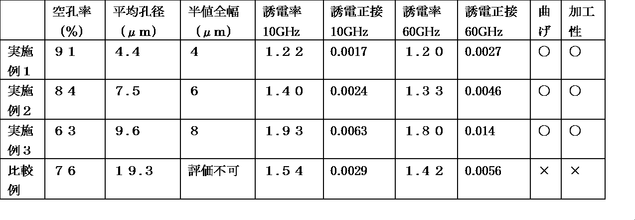
結果から明らかであるように、本発明によるフィルムは、高周波で低い誘電率及び誘電正接を示し、優れた電気的特性を有するものである。
また、実施例及び比較例で得られたフィルムについて、メッキ加工性を評価したところ、比較例で得られたフィルムの場合、液浸の問題があったが、実施例で得られたフィルムの場合にはそのような問題はなく、良好なメッキ加工を行うことができた。
さらに、本発明によるフィルムは、曲げ時の機械物性の点でも優れている。
また、実施例及び比較例で得られたフィルムについて、メッキ加工性を評価したところ、比較例で得られたフィルムの場合、液浸の問題があったが、実施例で得られたフィルムの場合にはそのような問題はなく、良好なメッキ加工を行うことができた。
さらに、本発明によるフィルムは、曲げ時の機械物性の点でも優れている。
次に、実施例4及び5で得られたフィルムの断面をSEMで観察した結果を、図5(実施例4)及び図6(実施例5)に示す。
SEM観察の結果から、実施例4及び5で得られたフィルムに形成されているスキン層の厚みは、表3に示すような厚みを有するものであった。
SEM観察の結果から、実施例4及び5で得られたフィルムに形成されているスキン層の厚みは、表3に示すような厚みを有するものであった。

さらに、実施例4及び5で得られたフィルムについて測定された結果を、表4に示す。
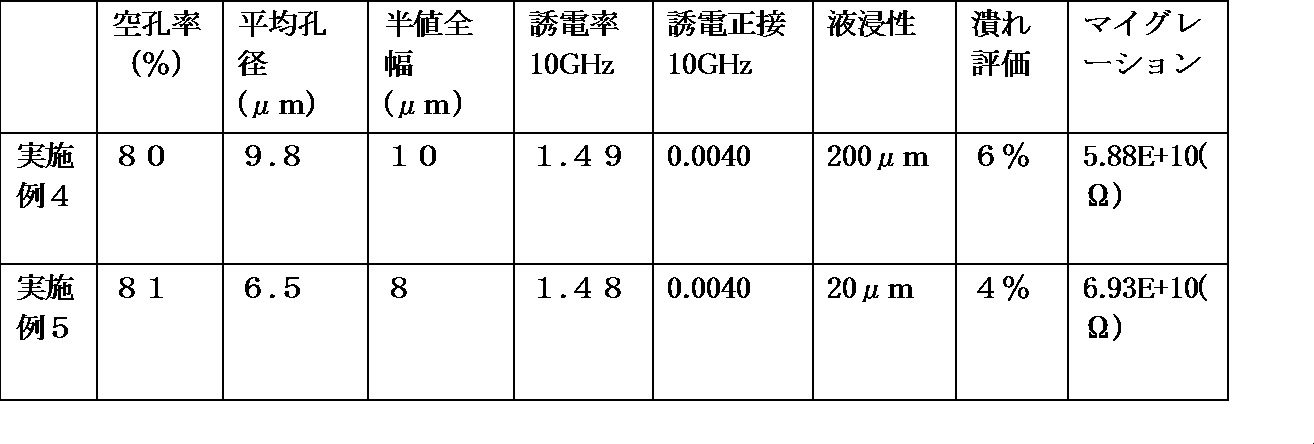
結果から明らかであるように、多孔構造が独泡構造である本発明によるフィルムは、優れた電気的特性を有するものであるとともに、液浸性や耐プレス性に優れ、加工後も高い絶縁抵抗値を示すことから、回路基板加工性の点でも優れている。
Claims (17)
- ポリマー材料からなるベース材料層に微細な空孔が分散形成された、多孔質の低誘電性ポリマーフィルムであって、
前記ベース材料層の少なくとも一方の表面に、該ベース材料層のポリマー材料からなる実質的に平滑なスキン層が形成されている、
ことを特徴とする、前記フィルム。 - 前記スキン層の厚さは前記フィルム全体の厚さの10%未満であることを特徴とする、請求項1に記載のフィルム。
- 前記スキン層の厚さは前記フィルム全体の厚さの5%以下であることを特徴とする、請求項2に記載のフィルム。
- 前記スキン層の厚さは1~5μmであることを特徴とする、請求項1~3のいずれか1項に記載のフィルム。
- 前記ベース材料層の両面に前記スキン層が形成されていることを特徴とする、請求項1~4のいずれか1項に記載のフィルム。
- 前記スキン層は液体不透過性であることを特徴とする、請求項1~5のいずれか1項に記載のフィルム。
- 前記ベース材料層の空孔率が60%以上であることを特徴とする、請求項1~6のいずれか1項に記載のフィルム。
- 前記ベース材料の空孔率が95%以下であることを特徴とする、請求項1~7のいずれか1項に記載のフィルム。
- 前記ベース材料層の平均孔径が10μm以下であることを特徴とする、請求項1~8のいずれか1項に記載のフィルム。
- 前記ベース材料層の孔径分布の半値全幅が10μm以下であることを特徴とする、請求項1~9のいずれか1項に記載のフィルム。
- 60GHzで測定した誘電率が2.0以下であることを特徴とする、請求項1~10のいずれか1項に記載のフィルム。
- 前記ポリマーが、該ポリマー又はその前駆体が有機溶媒に可溶性であるものであることを特徴とする、請求項1~11のいずれか1項に記載のフィルム。
- 前記有機溶媒がN-メチルピロリドンであることを特徴とする、請求項12に記載のフィルム。
- 前記ポリマーが、ポリイミド、ポリエーテルイミド、フッ化ポリイミド、及びポリカーボネートからなる群から選ばれることを特徴とする、請求項1~13のいずれか1項に記載のフィルム。
- 厚さが50μm~500μmであることを特徴とする、請求項1~14のいずれか1項に記載のフィルム。
- ミリ波アンテナ用の基板に使用するフィルムであることを特徴とする、請求項1~15のいずれか1項に記載のフィルム。
- 多孔構造が独泡構造であることを特徴とする、請求項1~16のいずれか1項に記載のフィルム。
Priority Applications (4)
| Application Number | Priority Date | Filing Date | Title |
|---|---|---|---|
| EP17833757.2A EP3489292B1 (en) | 2016-07-25 | 2017-04-06 | Low-dielectric porous polymer film and film for millimeter-wave antenna |
| KR1020197004006A KR102302832B1 (ko) | 2016-07-25 | 2017-04-06 | 다공질의 저유전성 폴리머 필름 및 밀리파 안테나용 필름 |
| US16/320,056 US20190263995A1 (en) | 2016-07-25 | 2017-04-06 | Low-dielectric porous polymer film and film for millimeter-wave antenna |
| CN201780046368.3A CN109496223B (zh) | 2016-07-25 | 2017-04-06 | 多孔的低介电性聚合物膜及毫米波天线用膜 |
Applications Claiming Priority (2)
| Application Number | Priority Date | Filing Date | Title |
|---|---|---|---|
| JP2016-145541 | 2016-07-25 | ||
| JP2016145541 | 2016-07-25 |
Publications (1)
| Publication Number | Publication Date |
|---|---|
| WO2018020746A1 true WO2018020746A1 (ja) | 2018-02-01 |
Family
ID=61016640
Family Applications (1)
| Application Number | Title | Priority Date | Filing Date |
|---|---|---|---|
| PCT/JP2017/014375 Ceased WO2018020746A1 (ja) | 2016-07-25 | 2017-04-06 | 多孔質の低誘電性ポリマーフィルム及びミリ波アンテナ用フィルム |
Country Status (7)
| Country | Link |
|---|---|
| US (1) | US20190263995A1 (ja) |
| EP (1) | EP3489292B1 (ja) |
| JP (3) | JP6567591B2 (ja) |
| KR (1) | KR102302832B1 (ja) |
| CN (1) | CN109496223B (ja) |
| TW (2) | TWI692890B (ja) |
| WO (1) | WO2018020746A1 (ja) |
Cited By (1)
| Publication number | Priority date | Publication date | Assignee | Title |
|---|---|---|---|---|
| WO2024111229A1 (ja) * | 2022-11-22 | 2024-05-30 | 日東電工株式会社 | 多孔質の低誘電性ポリマーフィルム |
Families Citing this family (16)
| Publication number | Priority date | Publication date | Assignee | Title |
|---|---|---|---|---|
| CN110475814B (zh) * | 2017-04-06 | 2022-09-13 | 日东电工株式会社 | 毫米波天线用膜 |
| KR102382750B1 (ko) * | 2018-03-27 | 2022-04-08 | 미쓰이금속광업주식회사 | 표면 처리 구리박, 동장 적층판 및 프린트 배선판의 제조 방법 |
| JP2020049905A (ja) * | 2018-09-28 | 2020-04-02 | 日東電工株式会社 | 低誘電基板材 |
| JP7082932B2 (ja) * | 2018-09-28 | 2022-06-09 | 日東電工株式会社 | 低誘電基板材 |
| JP7305328B2 (ja) * | 2018-10-01 | 2023-07-10 | 日東電工株式会社 | 多孔質体の製造方法 |
| JP7222727B2 (ja) * | 2019-01-24 | 2023-02-15 | 日東電工株式会社 | 低誘電基板材およびその製造方法 |
| CN114765917A (zh) * | 2021-01-13 | 2022-07-19 | 华为技术有限公司 | 印刷电路板及其制作方法,以及一种电子通讯设备 |
| JP7751974B2 (ja) * | 2021-02-15 | 2025-10-09 | 太陽ホールディングス株式会社 | 多孔質膜形成用ポリマー組成物、多孔質膜の製造方法、多孔質膜、フレキシブル金属張積層板及び電子基板 |
| JP7825815B2 (ja) * | 2021-03-22 | 2026-03-09 | 株式会社カナック | ポリイミド成形体の成形方法 |
| JP7700483B2 (ja) * | 2021-03-26 | 2025-07-01 | 富士フイルムビジネスイノベーション株式会社 | ポリイミド前駆体含有水性組成物、ポリイミド膜の製造方法、及び多孔質ポリイミド膜の製造方法 |
| WO2022211025A1 (ja) * | 2021-03-31 | 2022-10-06 | 三菱ケミカル株式会社 | 通信機器用成形体、及びポリシアヌレート |
| JP2022165324A (ja) * | 2021-04-19 | 2022-10-31 | 日東電工株式会社 | 金属層積層板用フィルム |
| CN117178012A (zh) * | 2021-04-19 | 2023-12-05 | 日东电工株式会社 | 低介电基板材料 |
| JP7846995B2 (ja) * | 2022-01-28 | 2026-04-16 | 日東電工株式会社 | 低誘電基板材 |
| KR20230174220A (ko) * | 2021-04-19 | 2023-12-27 | 닛토덴코 가부시키가이샤 | 저유전 기판재 |
| JP2023091635A (ja) * | 2021-12-20 | 2023-06-30 | 富士フイルムビジネスイノベーション株式会社 | ポリイミド前駆体溶液、多孔質ポリイミドフィルム、及び絶縁電線 |
Citations (5)
| Publication number | Priority date | Publication date | Assignee | Title |
|---|---|---|---|---|
| JP2001151929A (ja) * | 1999-11-29 | 2001-06-05 | Ube Ind Ltd | 多孔質ポリイミドフィルムの製造法及びフィルム |
| JP2004155933A (ja) * | 2002-11-07 | 2004-06-03 | Toray Ind Inc | 多孔性芳香族ポリアミド系フィルムおよびその製造方法 |
| JP2006111708A (ja) * | 2004-10-14 | 2006-04-27 | Inoac Corp | 低誘電率発泡材料とその製造方法 |
| WO2010038873A1 (ja) * | 2008-10-02 | 2010-04-08 | 宇部興産株式会社 | 多孔質ポリイミド膜及びその製造方法 |
| JP2014231533A (ja) * | 2011-02-03 | 2014-12-11 | 日東電工株式会社 | 多孔質樹脂成型体、多孔体基板およびその製造方法 |
Family Cites Families (17)
| Publication number | Priority date | Publication date | Assignee | Title |
|---|---|---|---|---|
| EP0052936A1 (en) * | 1980-11-07 | 1982-06-02 | Exxon Research And Engineering Company | Microcellular structures and process for their preparation |
| US5670102A (en) * | 1993-02-11 | 1997-09-23 | Minnesota Mining And Manufacturing Company | Method of making thermoplastic foamed articles using supercritical fluid |
| JP3115215B2 (ja) | 1995-10-05 | 2000-12-04 | 松下電器産業株式会社 | 低誘電率プラスチック絶縁フィルムおよびその製造方法 |
| JP4117986B2 (ja) * | 1999-06-07 | 2008-07-16 | 日東電工株式会社 | 耐熱性ポリマ発泡体とその製造法、及び発泡体基板 |
| JP4159199B2 (ja) | 1999-09-16 | 2008-10-01 | 日東電工株式会社 | 多孔質体及び多孔質体の製造方法 |
| JP4557409B2 (ja) | 2000-11-13 | 2010-10-06 | 日東電工株式会社 | 多孔質ポリイミドの製造方法及び多孔質ポリイミド |
| US7658989B2 (en) * | 2001-03-28 | 2010-02-09 | North Carolina State University | Nano-and micro-cellular foamed thin-walled material, and processes and apparatuses for making the same |
| JP4896309B2 (ja) * | 2001-07-13 | 2012-03-14 | 日東電工株式会社 | 多孔質ポリイミド樹脂の製造方法 |
| JP2003201362A (ja) * | 2002-01-09 | 2003-07-18 | Hitachi Ltd | 多孔質ポリイミドフィルムおよび多孔質ポリイミド回路基板 |
| JP2003201363A (ja) * | 2002-01-09 | 2003-07-18 | Hitachi Ltd | 多孔質ポリイミドフィルムとその配線基板及びその製造法並びにその用途 |
| JPWO2005061227A1 (ja) * | 2003-12-24 | 2007-12-13 | 帝人株式会社 | 積層体 |
| JP5179640B2 (ja) * | 2005-04-08 | 2013-04-10 | 日東電工株式会社 | 発泡部材 |
| JP5117150B2 (ja) * | 2007-09-21 | 2013-01-09 | 株式会社ダイセル | 多孔質層を有する積層体及びその製造方法、並びに多孔質膜及びその製造方法 |
| JP2012077294A (ja) * | 2010-09-11 | 2012-04-19 | Nitto Denko Corp | 多孔質樹脂シート及びその製造方法 |
| JP5734623B2 (ja) | 2010-11-10 | 2015-06-17 | ユニチカ株式会社 | 積層体の製造方法 |
| JP5916498B2 (ja) * | 2011-06-06 | 2016-05-11 | 日東電工株式会社 | ポリイミド多孔質体及びその製造方法 |
| CN109496222B (zh) * | 2016-07-25 | 2022-01-11 | 日东电工株式会社 | 毫米波天线用膜 |
-
2017
- 2017-04-06 CN CN201780046368.3A patent/CN109496223B/zh active Active
- 2017-04-06 WO PCT/JP2017/014375 patent/WO2018020746A1/ja not_active Ceased
- 2017-04-06 US US16/320,056 patent/US20190263995A1/en active Pending
- 2017-04-06 EP EP17833757.2A patent/EP3489292B1/en not_active Not-in-force
- 2017-04-06 KR KR1020197004006A patent/KR102302832B1/ko active Active
- 2017-04-06 JP JP2017076009A patent/JP6567591B2/ja active Active
- 2017-07-25 TW TW106124864A patent/TWI692890B/zh active
- 2017-07-25 TW TW109112465A patent/TWI740453B/zh active
-
2019
- 2019-07-31 JP JP2019140883A patent/JP2019199615A/ja active Pending
-
2021
- 2021-05-31 JP JP2021090948A patent/JP7179912B2/ja active Active
Patent Citations (5)
| Publication number | Priority date | Publication date | Assignee | Title |
|---|---|---|---|---|
| JP2001151929A (ja) * | 1999-11-29 | 2001-06-05 | Ube Ind Ltd | 多孔質ポリイミドフィルムの製造法及びフィルム |
| JP2004155933A (ja) * | 2002-11-07 | 2004-06-03 | Toray Ind Inc | 多孔性芳香族ポリアミド系フィルムおよびその製造方法 |
| JP2006111708A (ja) * | 2004-10-14 | 2006-04-27 | Inoac Corp | 低誘電率発泡材料とその製造方法 |
| WO2010038873A1 (ja) * | 2008-10-02 | 2010-04-08 | 宇部興産株式会社 | 多孔質ポリイミド膜及びその製造方法 |
| JP2014231533A (ja) * | 2011-02-03 | 2014-12-11 | 日東電工株式会社 | 多孔質樹脂成型体、多孔体基板およびその製造方法 |
Non-Patent Citations (1)
| Title |
|---|
| See also references of EP3489292A4 * |
Cited By (1)
| Publication number | Priority date | Publication date | Assignee | Title |
|---|---|---|---|---|
| WO2024111229A1 (ja) * | 2022-11-22 | 2024-05-30 | 日東電工株式会社 | 多孔質の低誘電性ポリマーフィルム |
Also Published As
| Publication number | Publication date |
|---|---|
| CN109496223A (zh) | 2019-03-19 |
| EP3489292B1 (en) | 2021-12-08 |
| CN109496223B (zh) | 2022-05-24 |
| TW201810753A (zh) | 2018-03-16 |
| EP3489292A1 (en) | 2019-05-29 |
| US20190263995A1 (en) | 2019-08-29 |
| JP6567591B2 (ja) | 2019-08-28 |
| TWI740453B (zh) | 2021-09-21 |
| TW202029544A (zh) | 2020-08-01 |
| EP3489292A4 (en) | 2020-03-04 |
| JP2019199615A (ja) | 2019-11-21 |
| JP2018021172A (ja) | 2018-02-08 |
| KR102302832B1 (ko) | 2021-09-15 |
| TWI692890B (zh) | 2020-05-01 |
| JP2021152165A (ja) | 2021-09-30 |
| JP7179912B2 (ja) | 2022-11-29 |
| KR20190027887A (ko) | 2019-03-15 |
Similar Documents
| Publication | Publication Date | Title |
|---|---|---|
| JP7179912B2 (ja) | ミリ波アンテナ用フィルム | |
| JP6567722B2 (ja) | ミリ波アンテナ用フィルム | |
| JP6567590B2 (ja) | ミリ波アンテナ用フィルム | |
| CN103597016B (zh) | 聚酰亚胺多孔体及其制造方法 | |
| KR20020037286A (ko) | 다공질 폴리이미드의 제조방법 및 다공질 폴리이미드 |
Legal Events
| Date | Code | Title | Description |
|---|---|---|---|
| 121 | Ep: the epo has been informed by wipo that ep was designated in this application |
Ref document number: 17833757 Country of ref document: EP Kind code of ref document: A1 |
|
| NENP | Non-entry into the national phase |
Ref country code: DE |
|
| ENP | Entry into the national phase |
Ref document number: 20197004006 Country of ref document: KR Kind code of ref document: A |
|
| ENP | Entry into the national phase |
Ref document number: 2017833757 Country of ref document: EP Effective date: 20190225 |