WO2018021238A1 - 検出チップ、検出システムおよび検出方法 - Google Patents
検出チップ、検出システムおよび検出方法 Download PDFInfo
- Publication number
- WO2018021238A1 WO2018021238A1 PCT/JP2017/026684 JP2017026684W WO2018021238A1 WO 2018021238 A1 WO2018021238 A1 WO 2018021238A1 JP 2017026684 W JP2017026684 W JP 2017026684W WO 2018021238 A1 WO2018021238 A1 WO 2018021238A1
- Authority
- WO
- WIPO (PCT)
- Prior art keywords
- detection
- light
- side wall
- metal film
- detection chip
- Prior art date
- Legal status (The legal status is an assumption and is not a legal conclusion. Google has not performed a legal analysis and makes no representation as to the accuracy of the status listed.)
- Ceased
Links
Images






Classifications
-
- G—PHYSICS
- G01—MEASURING; TESTING
- G01N—INVESTIGATING OR ANALYSING MATERIALS BY DETERMINING THEIR CHEMICAL OR PHYSICAL PROPERTIES
- G01N21/00—Investigating or analysing materials by the use of optical means, i.e. using sub-millimetre waves, infrared, visible or ultraviolet light
- G01N21/01—Arrangements or apparatus for facilitating the optical investigation
- G01N21/03—Cuvette constructions
- G01N21/0303—Optical path conditioning in cuvettes, e.g. windows; adapted optical elements or systems; path modifying or adjustment
-
- G—PHYSICS
- G01—MEASURING; TESTING
- G01N—INVESTIGATING OR ANALYSING MATERIALS BY DETERMINING THEIR CHEMICAL OR PHYSICAL PROPERTIES
- G01N21/00—Investigating or analysing materials by the use of optical means, i.e. using sub-millimetre waves, infrared, visible or ultraviolet light
- G01N21/01—Arrangements or apparatus for facilitating the optical investigation
- G01N21/03—Cuvette constructions
-
- B—PERFORMING OPERATIONS; TRANSPORTING
- B01—PHYSICAL OR CHEMICAL PROCESSES OR APPARATUS IN GENERAL
- B01L—CHEMICAL OR PHYSICAL LABORATORY APPARATUS FOR GENERAL USE
- B01L3/00—Containers or dishes for laboratory use, e.g. laboratory glassware; Droppers
- B01L3/50—Containers for the purpose of retaining a material to be analysed, e.g. test tubes
- B01L3/508—Rigid containers without fluid transport within
- B01L3/5082—Test tubes per se
-
- G—PHYSICS
- G01—MEASURING; TESTING
- G01N—INVESTIGATING OR ANALYSING MATERIALS BY DETERMINING THEIR CHEMICAL OR PHYSICAL PROPERTIES
- G01N21/00—Investigating or analysing materials by the use of optical means, i.e. using sub-millimetre waves, infrared, visible or ultraviolet light
- G01N21/62—Systems in which the material investigated is excited whereby it emits light or causes a change in wavelength of the incident light
- G01N21/63—Systems in which the material investigated is excited whereby it emits light or causes a change in wavelength of the incident light optically excited
- G01N21/64—Fluorescence; Phosphorescence
- G01N21/645—Specially adapted constructive features of fluorimeters
- G01N21/648—Specially adapted constructive features of fluorimeters using evanescent coupling or surface plasmon coupling for the excitation of fluorescence
-
- G—PHYSICS
- G01—MEASURING; TESTING
- G01N—INVESTIGATING OR ANALYSING MATERIALS BY DETERMINING THEIR CHEMICAL OR PHYSICAL PROPERTIES
- G01N21/00—Investigating or analysing materials by the use of optical means, i.e. using sub-millimetre waves, infrared, visible or ultraviolet light
- G01N21/62—Systems in which the material investigated is excited whereby it emits light or causes a change in wavelength of the incident light
- G01N21/63—Systems in which the material investigated is excited whereby it emits light or causes a change in wavelength of the incident light optically excited
- G01N21/64—Fluorescence; Phosphorescence
- G01N21/6486—Measuring fluorescence of biological material, e.g. DNA, RNA, cells
-
- G—PHYSICS
- G01—MEASURING; TESTING
- G01N—INVESTIGATING OR ANALYSING MATERIALS BY DETERMINING THEIR CHEMICAL OR PHYSICAL PROPERTIES
- G01N33/00—Investigating or analysing materials by specific methods not covered by groups G01N1/00 - G01N31/00
- G01N33/48—Biological material, e.g. blood, urine; Haemocytometers
- G01N33/50—Chemical analysis of biological material, e.g. blood, urine; Testing involving biospecific ligand binding methods; Immunological testing
- G01N33/53—Immunoassay; Biospecific binding assay; Materials therefor
- G01N33/543—Immunoassay; Biospecific binding assay; Materials therefor with an insoluble carrier for immobilising immunochemicals
-
- G—PHYSICS
- G01—MEASURING; TESTING
- G01N—INVESTIGATING OR ANALYSING MATERIALS BY DETERMINING THEIR CHEMICAL OR PHYSICAL PROPERTIES
- G01N33/00—Investigating or analysing materials by specific methods not covered by groups G01N1/00 - G01N31/00
- G01N33/48—Biological material, e.g. blood, urine; Haemocytometers
- G01N33/50—Chemical analysis of biological material, e.g. blood, urine; Testing involving biospecific ligand binding methods; Immunological testing
- G01N33/68—Chemical analysis of biological material, e.g. blood, urine; Testing involving biospecific ligand binding methods; Immunological testing involving proteins, peptides or amino acids
-
- B—PERFORMING OPERATIONS; TRANSPORTING
- B01—PHYSICAL OR CHEMICAL PROCESSES OR APPARATUS IN GENERAL
- B01L—CHEMICAL OR PHYSICAL LABORATORY APPARATUS FOR GENERAL USE
- B01L2300/00—Additional constructional details
- B01L2300/16—Surface properties and coatings
- B01L2300/168—Specific optical properties, e.g. reflective coatings
-
- G—PHYSICS
- G01—MEASURING; TESTING
- G01N—INVESTIGATING OR ANALYSING MATERIALS BY DETERMINING THEIR CHEMICAL OR PHYSICAL PROPERTIES
- G01N21/00—Investigating or analysing materials by the use of optical means, i.e. using sub-millimetre waves, infrared, visible or ultraviolet light
- G01N21/17—Systems in which incident light is modified in accordance with the properties of the material investigated
- G01N21/59—Transmissivity
- G01N2021/5903—Transmissivity using surface plasmon resonance [SPR], e.g. extraordinary optical transmission [EOT]
-
- G—PHYSICS
- G01—MEASURING; TESTING
- G01N—INVESTIGATING OR ANALYSING MATERIALS BY DETERMINING THEIR CHEMICAL OR PHYSICAL PROPERTIES
- G01N21/00—Investigating or analysing materials by the use of optical means, i.e. using sub-millimetre waves, infrared, visible or ultraviolet light
- G01N21/62—Systems in which the material investigated is excited whereby it emits light or causes a change in wavelength of the incident light
- G01N21/63—Systems in which the material investigated is excited whereby it emits light or causes a change in wavelength of the incident light optically excited
- G01N21/64—Fluorescence; Phosphorescence
- G01N21/645—Specially adapted constructive features of fluorimeters
- G01N2021/6482—Sample cells, cuvettes
Definitions
- the present invention relates to a detection chip, a detection system, and a detection method for detecting a substance to be detected.
- Biochemical reactions such as antigen-antibody reactions are used in biochemical tests.
- a fluorescence immunoassay hereinafter also referred to as “FIA”
- FIA fluorescence immunoassay
- a labeling substance containing a fluorescent substance is reacted with a substance to be detected (antigen).
- the target substance labeled with the fluorescent substance is irradiated with excitation light, and the fluorescence emitted from the fluorescent substance is detected.
- the amount of the substance to be detected is specified from the detected fluorescence intensity or the like.
- SPFS surface plasmon-excited fluorescence spectroscopy
- SPFS surface plasmon-excited fluorescence spectroscopy
- a first capturing body (for example, a primary antibody) that can specifically bind to a substance to be detected is fixed on a metal film to form a reaction field for capturing the substance to be detected.
- the reaction field is arranged on the bottom surface of a well (a bottomed recess for containing a liquid).
- a well is formed by fixing a well member having a through hole on a metal film formed on a dielectric member having light transmittance. Is disposed on the metal film constituting the bottom surface of the well. Then, by introducing a liquid (specimen) containing the substance to be detected into the well, the substance to be detected is bound to the first capturing body.
- a second capture body labeled with a fluorescent substance is introduced into the well, whereby the second capture body is further bound to the detection target substance bound to the first capture body.
- the substance to be detected is indirectly labeled with a fluorescent substance.
- the fluorescent material is excited by an electric field enhanced by surface plasmon resonance (hereinafter also referred to as “SPR”), and emits fluorescence.
- SPR surface plasmon resonance
- the substance to be detected can be detected by detecting the fluorescence emitted by the fluorescent substance.
- the detection unit for detecting fluorescence is arranged above the well and detects fluorescence that has passed through the liquid surface of the liquid in the well.
- the detection unit is disposed above the well and detects fluorescence that has passed through the liquid surface of the liquid in the well. For this reason, when the inner diameter of the well is small, the fluorescence detection result is affected by the meniscus. Further, even if the inner diameter of the well is large, the fluorescence detection result may be affected by bubbles present on the liquid surface.
- An object of the present invention is to suppress a decrease in detection accuracy due to the remaining liquid in the container (well) during the reaction process, and to affect the detection result due to the liquid level of the liquid in the container during the detection process. It is to provide a detection chip, a detection system, and a detection method for detecting a substance to be detected.
- a detection chip includes a well main body including an accommodating portion having openings on the top and side portions, and a side wall member in which a capture region for capturing a substance to be detected is disposed.
- the side wall member exposes at least a part of the capturing region through the opening in the side part of the housing part, and the side wall member covers at least a part of the opening in the side part of the housing part.
- the well body is fixed so as to be closed.
- the detection system is disposed without a metal film or via a metal film on the inner surface of the housing part having an opening in the upper part and the side wall constituting the housing part,
- a detection chip having a reaction field for capturing a substance to be detected, and an external so that evanescent light is generated on the inner surface of the side wall at a position corresponding to the reaction field, or surface plasmon resonance is generated in the metal film
- a detector that detects light whose amount of light changes according to the amount.
- the detection method includes a housing part having an opening in the upper part and a reaction arranged on the inner surface of the side wall constituting the housing part without or through the metal film.
- the present invention it is possible to suppress a decrease in detection accuracy due to the remaining liquid in the container during the reaction process, and to suppress the influence on the detection result due to the liquid level of the liquid in the container during the detection process. It is possible to provide a detection chip, a detection system, and a detection method for detecting a substance to be detected.
- FIG. 1 is a schematic diagram illustrating a configuration of a detection system according to the first embodiment.
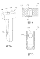
- 2A is a perspective view of the detection chip according to Embodiment 1
- FIG. 2B is a perspective view of the well body
- FIG. 2C is a perspective perspective view of the well body.
- 3A and 3B are schematic diagrams showing light incident on the detection chip and light emitted from the detection chip according to Embodiment 1.
- FIG. FIG. 4 is a partially enlarged sectional view in which the vicinity of the reaction field in the sectional view of FIG. 3A is enlarged.
- 5A to 5D are cross-sectional views of the detection chip showing examples of the shape of the side wall facing the reaction field.
- FIG. 6A is a perspective view of a detection chip according to the first modification
- FIG. 6B is a perspective view of a well body according to the first modification.
- 7A is a perspective view of a well body according to a second modification
- FIG. 7B is a cross-sectional view along the horizontal direction of the well body according to the second modification
- FIG. 7C is according to the second modification. It is sectional drawing in alignment with the height direction of the bottom part vicinity of a well main body.
- 8A to 8C are cross-sectional views showing examples of a detection chip having a plurality of accommodating portions.
- FIG. 9 is a flowchart of the detection method according to the first embodiment, and is a flowchart illustrating an example of an operation procedure of the detection system.
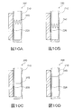
- FIGS. 10A and 10B are schematic diagrams showing the relationship between the reaction field and the liquid level when the detection chip is vibrated, and FIGS. 10C and 10D show the reaction field and the liquid level when detecting fluorescence. It is a schematic diagram which shows the relationship.
- FIG. 11 is a schematic diagram illustrating a configuration of a detection system according to the second embodiment.
- 12A is a perspective view of the detection chip according to Embodiment 2
- FIG. 12B is a perspective view of the well body
- FIG. 12C is a perspective perspective view of the well body.
- FIG. 13 is a schematic diagram showing light incident on the detection chip and light emitted from the detection chip according to the second embodiment.
- FIG. 14 is a partially enlarged sectional view in which the vicinity of the reaction field in the sectional view of FIG. 13 is enlarged.
- 15A and 15B are perspective views of the diffraction grating.
- FIG. 16 is a flowchart of the detection method according to the second embodiment, and is a flowchart illustrating an example of an operation procedure of the detection system.
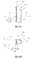
- FIG. 17A and FIG. 17B are schematic views showing light incident on the detection chip and light emitted from the detection chip for explaining a first modification of the detection system according to Embodiment 2.
- FIG. 18A and FIG. 18B are schematic diagrams showing light incident on the detection chip and light emitted from the detection chip for explaining a second modification of the detection system according to Embodiment 2.
- a detection chip, a detection system, and a detection method for detecting a substance to be detected by SPFS will be described as an embodiment of a detection chip, a detection system, and a detection method according to the present invention.
- the detection chip, the detection system, and the detection method are not limited to this.
- Embodiment 1 a detection chip, a detection system, and a detection method for detecting a substance to be detected by a prism-coupled SPFS (PC-SPFS) that generates SPR using a prism will be described.
- PC-SPFS prism-coupled SPFS
- FIG. 1 is a schematic diagram illustrating a configuration of a detection system 100 according to the first embodiment.
- the detection system 100 operates in a state where the detection chip 200 is mounted at a predetermined position.
- the detection system 100 includes an excitation light irradiation unit 110, a fluorescence detection unit 120, a liquid feeding unit 130, a vibration unit 140, and a control unit 150.
- the detection chip 200 is irradiated with excitation light ⁇ so that surface plasmon resonance occurs in the metal film 225 of the detection chip 200 with the detection chip 200 mounted at a predetermined position, and in the vicinity of the metal film 225.
- An enhanced electric field based on surface plasmon resonance is generated.
- the presence or amount of the substance to be detected in the specimen is measured by exciting the fluorescent substance existing in the reaction field 226 on the metal film 225 with the enhanced electric field and detecting the fluorescence ⁇ emitted from the fluorescent substance.
- the detection chip 200 will be described first, and then the detection system 100 and its operation (detection method) will be described.
- FIG. 2A to 2C are schematic diagrams showing the configuration of the detection chip 200 according to Embodiment 1.
- FIG. 2A is a perspective view of the detection chip 200
- FIG. 2B is a perspective view of the well body 210
- FIG. 2C is a perspective perspective view of the well body 210.
- 3A and 3B are schematic diagrams showing light (excitation light ⁇ ) incident on the detection chip 200 and light (fluorescence ⁇ and plasmon scattered light ⁇ ) emitted from the detection chip 200.
- FIG. 3A is a cross-sectional view along the height direction of the detection chip 200
- FIG. 3B is a cross-sectional view along the horizontal direction of the detection chip 200.
- FIG. 3A and 3B show a state in which a liquid (for example, a measurement buffer solution) is stored in the storage portion 211.
- FIG. FIG. 4 is a partially enlarged sectional view in which the vicinity of the reaction field 226 in the sectional view of FIG. 3A is enlarged.
- the detection chip 200 includes a well body 210 and a side wall member 220.
- the well body 210 has a housing part (well) 211 therein.
- the accommodating part 211 is a bottomed concave part configured to be able to accommodate a liquid, and is opened to the outside by a first opening 212 provided in the upper part and a second opening 213 provided in the side part.
- the first opening 212 is used when introducing a liquid into the storage unit 211 or removing the liquid from the storage unit 211.
- the second opening 213 is formed in order to form a reaction field 226 by exposing a capture region 227 of the side wall member 220 to be described later into the accommodating portion 211 (see FIG. 4).
- the second opening 213 is closed by the side wall member 220 so that the liquid can be stored in the storage portion 211.
- the second opening 213 is a through hole formed in the side wall on the side wall member 220 side among the four side walls constituting the accommodating portion 211.
- detection chip 200 In detection chip 200 according to the present embodiment, light (fluorescence ⁇ and plasmon scattered light ⁇ ) emitted from the vicinity of reaction field 226 passes through the side wall facing reaction field 226 and is detected by detection unit 125 described later. (See FIG. 1). Therefore, when it is desired to suppress the refraction of the light to be detected, as shown in FIG. 5A, the inner surface and the outer surface of the side wall facing the reaction field 226 (capturing region 227) in the accommodating portion are both flat. Is preferred. On the other hand, when it is desired to collect the light to be detected toward the detection unit 125, as shown in FIGS.
- At least one of the inner surface and the outer surface of the side wall facing the reaction field 226 in the housing portion is a convex curved surface. It is preferable that In the example shown in FIG. 5B, only the inner surface of the side wall is a convex curved surface, and the side wall facing the reaction field 226 functions as a plano-convex cylindrical lens. In the example shown in FIG. 5C, only the outer surface of the side wall is a convex curved surface, and the side wall facing the reaction field 226 functions as a plano-convex cylindrical lens. In the example shown in FIG. 5D, the inner surface and the outer surface of the side wall are both convex curved surfaces, and the side wall facing the reaction field 226 functions as a biconvex cylindrical lens.
- the shape of the well main body 210 is not particularly limited as long as it has the accommodating portion 211, the first opening 212, and the second opening 213.
- FIG. 6A is a perspective view of the detection chip 200 according to the first modification
- FIG. 6B is a perspective view of the well body 210 according to the first modification.
- the second opening 213 may be formed on the entire surface on the side wall member 220 side, or may be connected to the first opening 212. Also in this case, at least a part of the second opening 213 is closed by the side wall member 220 so that the liquid can be stored in the storage portion 211.
- FIG. 7A is a perspective view of a well body 210 according to a second modification
- FIG. 7B is a cross-sectional view along the horizontal direction of the well body 210 according to the second modification
- FIG. 7C is a second modification. It is sectional drawing in alignment with the height direction of the bottom part vicinity of the well main body 210 which concerns on.
- the well body 210 may further include a holding portion 214 that protrudes laterally from the upper portion thereof.
- the detection chip 200 has the holding unit 214 as described above, the user and the system can grip the holding unit, so that the detection chip 200 can be handled more easily. Further, as shown in FIG.
- all or a part of the inner surfaces of the side walls other than the side wall facing the reaction field 227 among the four side walls constituting the accommodating portion 211 are curved surfaces curved in the circumferential direction. May be.
- the cross-sectional shape along the horizontal direction of the accommodating part 211 is substantially polygonal shape (for example, substantially square shape) (refer FIG. 3B).
- the convex part for example, round bottom
- the well body 210 is made of a material that is transparent to light (at least the light having the wavelength of the excitation light ⁇ and the light having the wavelength of the fluorescence ⁇ ). However, a part of the well body 210 may be made of a material that is opaque to light as long as it does not interfere with light extraction in the detection method described later. At least the side wall that faces the reaction field 226 among the four side walls that form the housing portion 211 has light transmittance. Examples of materials that are transparent to light include resin and glass.
- the side wall member 220 includes a prism 221 as an optical element, a metal film 225, and a reaction field 226.
- the “reaction field” means a region exposed in the accommodating portion 211 through the second opening 213 in the capture region 227 disposed on the metal film 225 (see FIG. 4).
- the side wall member 220 has a reaction field 226 in which at least a part of the capture region 227 is exposed in the accommodating portion 211, and the side wall member 220 is second. It is fixed to the well body 210 so as to completely close at least a part of the opening 213.
- the side wall member 220 is bonded to the well body 210 through an adhesive layer (not shown) such as a double-sided tape so as to close the entire second opening 213.
- the side wall member 220 may be joined to the well body 210 by laser welding, ultrasonic welding, pressure bonding using a clamp member, or the like without using an adhesive layer.
- the prism 221 is an optical element made of a dielectric that is transparent to the excitation light ⁇ , and has an incident surface 222, a reflective surface 223, and an output surface 224, as shown in FIG. 3B.
- the prism 221 also functions as a side wall that constitutes the housing portion 211.
- the incident surface 222 is a surface for causing the excitation light ⁇ from the excitation light irradiation unit 110 to enter the prism 221.
- the excitation light ⁇ that has entered the prism 221 is reflected by the reflecting surface 223.
- a metal film 225 and a capture region 227 are sequentially arranged on the reflection surface 223.
- the emission surface 224 is a surface for emitting the reflected light ⁇ ′ reflected by the reflection surface 223 to the outside of the prism 221.
- the shape of the prism 221 is not particularly limited, but the reflecting surface 223 is preferably a flat surface.
- Examples of the shape of the prism 221 include a columnar body having a trapezoidal bottom surface, a triangular prism, and a semi-cylinder.
- the shape of the prism 221 is a column having a trapezoidal bottom surface.
- the surface corresponding to one base of the trapezoid is the reflecting surface 223, the surface corresponding to one leg is the entrance surface 222, and the surface corresponding to the other leg is the exit surface 224.
- the incident surface 222 is formed so that the excitation light ⁇ does not return to the excitation light irradiation unit 110.
- the light source of the excitation light ⁇ is a laser diode (hereinafter also referred to as “LD”)
- LD laser diode
- the angle of the incident surface 222 is set so that the excitation light ⁇ does not enter the incident surface 222 perpendicularly in a scanning range centered on an ideal resonance angle or enhancement angle.
- the “resonance angle” means that when the incident angle of the excitation light ⁇ with respect to the reflection surface 223 (metal film 225) is scanned, the amount of the reflected light ⁇ ′ emitted from the emission surface 224 is minimized. It means the incident angle.
- the “enhancement angle” is the same wavelength as the excitation light ⁇ emitted from the periphery of the reaction field 226 into the accommodating portion 211 when the incident angle of the excitation light ⁇ with respect to the reflection surface 223 (metal film 225) is scanned. It means the incident angle when the amount of scattered light (plasmon scattered light) ⁇ becomes maximum.
- the angle between the incident surface 222 and the reflecting surface 223 and the angle between the reflecting surface 223 and the emitting surface 224 are both about 80 °.
- the resonance angle (and the enhancement angle near the pole) is generally determined by the design of the detection chip 200.
- the design factors are the refractive index of the prism 221, the refractive index of the metal film 225, the thickness of the metal film 225, the extinction coefficient of the metal film 225, the wavelength of the excitation light ⁇ , and the like.
- the resonance angle and the enhancement angle are shifted by the detected substance trapped in the reaction field 226 (capture region 227) on the metal film 225, but the amount is less than a few degrees.
- the prism 221 has a considerable amount of birefringence.
- Examples of the material of the prism 221 include resin and glass.
- the material of the prism 221 is preferably a resin having a refractive index of 1.4 to 1.6 and a small birefringence.
- the metal film 225 is disposed on the reflection surface 223 of the prism 221.
- an interaction SPR
- the enhancement is localized on the surface of the metal film 225.
- An electric field is generated.
- the material of the metal film 225 is not particularly limited as long as it is a metal that can cause surface plasmon resonance.
- Examples of the material of the metal film 225 include gold, silver, copper, aluminum, and alloys thereof.
- a method for forming the metal film 225 is not particularly limited. Examples of the method for forming the metal film 225 include sputtering, vapor deposition, and plating.
- the thickness of the metal film 225 is not particularly limited, but is preferably in the range of 30 to 70 nm.
- the reaction field 226 is an area for capturing the substance to be detected, which is exposed in the container 211.
- the reaction field 226 means a region exposed in the accommodating portion 211 through the second opening 213 in the capturing region 227 disposed on the metal film 225.
- the range of the reaction field 226 is defined by the second opening 213.
- a capturing region 227 having a predetermined shape is formed on a part of the surface of the metal film 225, and this capturing is performed.
- the region 227 becomes the reaction field 226 as it is.
- the reaction field 226 is disposed on the inner side surface of the housing part 211. At this time, the reaction field 226 is preferably arranged at a position away from the deepest part of the housing part 211. With such a configuration, a reaction can be efficiently generated in the reaction field 226 when a sample or the like is introduced into the storage unit 211. In addition, it is possible to suppress noise caused by the bottom of the accommodating portion 211 from being mixed with the detection result when detecting the fluorescence ⁇ .
- the capture area 227 is an area where a first capture body for capturing a substance to be detected is immobilized on the metal film 225.
- the first capturing body is a substance having a recognition site for specifically binding to the substance to be detected in the specimen.
- the detection target substance is selectively bound to the first capture body. That is, the substance to be detected is captured in the reaction field 226. This makes it possible to detect the substance to be detected as will be described later.
- the type of the first capturing body is not particularly limited as long as it has a recognition site for specifically binding to the substance to be detected. Examples of the first capturing body include an antibody (primary antibody) or a fragment thereof that can specifically bind to the substance to be detected, an enzyme that can specifically bind to the substance to be detected, and the like.
- the surface on which the capture region 227 is arranged in the region to be the reaction field 226 is a flat surface. That is, when the capture region 227 is disposed on the metal film 225 as in the present embodiment, the surface of the metal film 225 is preferably a flat surface. Further, as described at the end of the present embodiment, when the capture region 227 is disposed on the reflection surface 223, the reflection surface 223 is preferably a flat surface.
- the detection chip 200 may further include a second storage unit 230 that can store a liquid in addition to the storage unit 211.
- the use of the 2nd accommodating part 230 is not specifically limited.
- the reagent used in the reaction process or the detection process may be stored in the second storage unit 230 in advance.
- two or more types of reagents may be mixed in the second storage unit 230.
- the number and position of the second storage units 230 are not particularly limited as long as they do not hinder the detection of the detection target substance.
- one second housing portion 230 may be added to the side wall on the side wall member 220 side among the four side walls constituting the housing portion 211.
- one second housing portion 230 may be added to the side wall facing the reaction field 226 among the four side walls constituting the housing portion 211.
- a plurality of second accommodating portions 230 may be added to one of the four sidewalls constituting the accommodating portion 211.
- the detection chip 200 The planar view shape is substantially rectangular, and a plurality of detection chips 200 can be efficiently accommodated in the storage container.
- the detection system 100 includes the excitation light irradiation unit 110, the fluorescence detection unit 120, the liquid supply unit 130, the vibration unit 140, and the control unit 150 in addition to the detection chip 200 (see FIG. 1).
- the excitation light irradiation unit 110 irradiates the detection chip 200 with excitation light ⁇ .
- the excitation light irradiation unit 110 reflects the reflection surface 223 so that the incident angle with respect to the reflection surface 223 (metal film 225) of the prism 221 is an angle that causes SPR in the metal film 225. Only the P wave for (metal film 225) is emitted toward the incident surface 222 of the prism 221.
- the “excitation light” is light that directly or indirectly excites the fluorescent material.
- the excitation light irradiation unit 110 includes a light source unit 111 and a first angle adjustment unit 112.
- the light source unit 111 emits the collimated excitation light ⁇ having a constant wavelength and light amount so that the shape of the irradiation spot on the reflection surface 223 (the surface of the metal film 225) is substantially circular.
- the size of the irradiation spot is preferably smaller than the reaction field 226 of the detection chip 200.
- the light source unit 111 includes, for example, a light source of excitation light ⁇ , a beam shaping optical system, an APC mechanism, and a temperature adjustment mechanism (all not shown).
- the type of the light source is not particularly limited, and is, for example, a laser diode (LD).
- Other examples of light sources include light emitting diodes, mercury lamps, and other laser light sources.
- the light emitted from the light source is not a beam, the light emitted from the light source is converted into a beam by a lens, a mirror, a slit, or the like.
- the light emitted from the light source is not monochromatic light, the light emitted from the light source is converted into monochromatic light by a diffraction grating or the like.
- the light emitted from the light source is not linearly polarized light, the light emitted from the light source is converted into linearly polarized light by a polarizer or the like.
- the beam shaping optical system includes, for example, a collimator, a band pass filter, a linear polarization filter, a half-wave plate, a slit, and a zoom means.
- the beam shaping optical system may include all of these or a part thereof.
- the collimator collimates the excitation light ⁇ emitted from the light source.
- the band-pass filter turns the excitation light ⁇ emitted from the light source into narrowband light having only the center wavelength. This is because the excitation light ⁇ from the light source has a slight wavelength distribution width.
- the linear polarization filter turns the excitation light ⁇ emitted from the light source into completely linearly polarized light.
- the half-wave plate adjusts the polarization direction of the excitation light ⁇ so that the P-wave component is incident on the reflection surface 223.
- the slit and zoom means adjust the beam diameter, contour shape, and the like of the excitation light ⁇ so that the shape of the irradiation spot on the reflection surface 223 becomes a circle of a predetermined size.
- the APC mechanism controls the light source so that the output of the light source is constant. More specifically, the APC mechanism detects the amount of light branched from the excitation light ⁇ with a photodiode (not shown) or the like. The APC mechanism controls the input energy by a regression circuit, thereby controlling the output of the light source to be constant.
- the temperature adjustment mechanism is, for example, a heater or a Peltier element.
- the wavelength and energy of the light emitted from the light source may vary depending on the temperature. For this reason, the wavelength and energy of the light emitted from the light source are controlled to be constant by keeping the temperature of the light source constant by the temperature adjusting mechanism.
- the first angle adjustment unit 112 adjusts the incident angle of the excitation light ⁇ with respect to the reflection surface 223.
- the first angle adjustment unit 112 causes the optical axis of the excitation light ⁇ and the detection chip 200 to be relative to each other so as to irradiate the excitation light ⁇ at a predetermined incident angle toward a predetermined position on the reflection surface 223 via the prism 221. Rotate.
- the first angle adjustment unit 112 rotates the light source unit 111 around an axis (axis along the height direction of the detection chip 200) orthogonal to the optical axis of the excitation light ⁇ (see FIG. 3B). At this time, the position of the rotation axis is set so that the position of the irradiation spot on the reflecting surface 223 hardly changes even when the incident angle is scanned.
- the angle at which the amount of plasmon scattered light ⁇ is maximum is the enhancement angle.
- an enhancement angle or an angle in the vicinity thereof for example, a resonance angle
- the basic incident condition of the excitation light ⁇ is determined by the material and shape of the prism 221 of the detection chip 200, the film thickness of the metal film 225, the refractive index of the liquid in the container 211, and the like. The optimum incident condition varies slightly depending on the amount and the shape error of the prism 221. For this reason, it is preferable to obtain an optimal enhancement angle for each detection.
- the fluorescence detection unit 120 detects the fluorescence ⁇ generated by the irradiation of the excitation light ⁇ to the reflection surface 223 (metal film 225). Further, as necessary, the fluorescence detection unit 120 also detects the plasmon scattered light ⁇ generated by the irradiation of the excitation light ⁇ onto the reflection surface 223 (metal film 225).
- the fluorescence detection unit 120 includes a first lens 121, an optical filter 122, a second lens 123, a position switching unit 124, and a detection unit 125.
- the first lens 121 is, for example, a condensing lens, and condenses light emitted from the vicinity of the reaction field 226.
- the second lens 123 is, for example, an imaging lens, and forms an image of the light collected by the first lens 121 on the light receiving surface of the detection unit 125.
- the optical path between both lenses is a substantially parallel optical path.
- the optical filter 122 is disposed between both lenses.
- the optical filter 122 guides only the fluorescence component to the detection unit 125 and removes the excitation light component (plasmon scattered light ⁇ ) in order to detect the fluorescence ⁇ with a high S (signal) / N (noise) ratio.
- the optical filter 122 include an excitation light reflection filter, a short wavelength cut filter, and a band pass filter.
- the optical filter 122 is, for example, a filter including a multilayer film that reflects a predetermined light component, or a color glass filter that absorbs a predetermined light component.
- the position switching unit 124 switches the position of the optical filter 122 on or off the optical path between the first lens 121 and the second lens 123. Specifically, when the detection unit 125 detects the fluorescence ⁇ , the optical filter 122 is disposed on the optical path, and when the detection unit 125 detects the plasmon scattered light ⁇ , the optical filter 122 is disposed outside the optical path.
- the detection unit 125 is a light receiving sensor that detects fluorescence ⁇ and plasmon scattered light ⁇ .
- the detection unit 125 has high sensitivity capable of detecting weak fluorescence ⁇ from a minute amount of a substance to be detected.
- the detection unit 125 is, for example, a photomultiplier tube (PMT) or an avalanche photodiode (APD).
- the excitation light ⁇ from the light source unit 111 travels in the horizontal direction and reaches the detection chip 200. Further, light (fluorescence ⁇ and plasmon scattered light ⁇ ) emitted from the vicinity of the reaction field 226 and traveling in the horizontal direction is detected by the detection unit 125. Therefore, in the present embodiment, the light source unit 111 and the detection unit 125 are arranged at the same height as the detection chip 200. Of course, if a mirror or the like is used, the positions of the light source unit 111 and the detection unit 125 can be freely changed. However, from the viewpoint of miniaturization, the light source unit 111 and the detection unit 125 are arranged at the same height as the detection chip 200. It is preferable that
- the liquid feeding unit 130 introduces various liquids into the accommodating portion 211 of the detection chip 200.
- the liquid feeding unit 130 removes various liquids from the inside of the housing part 211 of the detection chip 200.
- the liquid feeding unit 130 injects, for example, a specimen, a labeling liquid (hereinafter also referred to as “labeling liquid”) containing a second capturing body labeled with a fluorescent substance, a cleaning liquid, a measurement buffer, and the like. And do suction.
- the liquid feeding unit 130 includes a liquid tip 131, a pipette 132, and a pipette control unit 136.
- the liquid chip 131 is a container for storing a liquid such as a specimen, a labeling liquid, a cleaning liquid, and a measurement buffer.
- a liquid chip 131 a plurality of containers are usually arranged according to the type of liquid, or a chip in which a plurality of containers are integrated is arranged.
- the detection chip 200 includes the second storage unit 230
- the second storage unit 230 can function as the liquid chip 131.
- the liquid feeding unit 130 may not have the liquid chip 131.
- the pipette 132 has a syringe pump 133, a nozzle unit 134 connected to the syringe pump 133, and a pipette tip 135 attached to the tip of the nozzle unit 134.
- the pipette control unit 136 includes a driving device for the syringe pump 133 and a moving device for the nozzle unit 134.
- the drive device of the syringe pump 133 is a device for reciprocating the plunger of the syringe pump 133 and includes, for example, a stepping motor.
- the moving device of the nozzle unit 134 moves the nozzle unit 134 freely in two directions, a vertical direction and a horizontal direction.
- the moving device of the nozzle unit 134 is constituted by, for example, a robot arm, a two-axis stage, or a turntable that can move up and down.
- the pipette controller 136 drives the syringe pump 133 to suck various liquids from the liquid tip 131 into the pipette tip 135. Then, the pipette control unit 136 moves the nozzle unit 134 to insert the pipette tip 135 into the housing portion 211 of the detection chip 200 from the first opening 212 and drives the syringe pump 133 to move the pipette tip 135 inside. The liquid is injected into the container 211. In addition, after the introduction of the liquid, the pipette control unit 136 drives the syringe pump 133 to suck the liquid in the storage unit 211 into the pipette tip 135.
- the first capturing body reacts with the substance to be detected in the reaction field 226 (primary reaction), or the first substance labeled with the substance to be detected and the fluorescent substance is reacted.
- the second capturing body is reacted (secondary reaction).
- the vibration unit 140 vibrates the detection chip 200 in order to agitate the liquid in the storage unit 211. In this way, by vibrating the detection chip 200 and stirring the liquid in the storage unit 211, primary reaction, secondary reaction, washing, and the like in the reaction field 226 can be performed efficiently.
- the vibration unit 140 is, for example, a piezoelectric element or an eccentric rotating body.
- the excitation unit 140 is disposed at a position that does not interfere with the optical paths of the excitation light ⁇ , fluorescence ⁇ , and plasmon scattered light ⁇ .
- the direction of vibration applied to the detection chip 200 by the vibration unit 140 is not particularly limited.
- the vibration direction include a horizontal direction, a vertical direction (height direction), and a circumferential direction.
- the reciprocating vibration in the horizontal direction can be applied to the detection chip 200 by driving the piezo element in a state where the piezo element as the vibration unit 140 is in contact with the side surface of the detection chip 200.
- vertical reciprocation vibration can be applied to the detection chip 200.
- the detection chip 200 is vibrated at the natural frequency of the detection chip 200 in the state in which the liquid is stored in the storage unit 211, or the vibration frequency before and after that. Is preferred.
- the detection chip 200 may be vibrated while sequentially switching different natural frequencies (n-th natural frequency and m-th natural frequency, where n and m are positive integers).
- the control unit 150 controls the light source unit 111, the first angle adjustment unit 112, the position switching unit 124, the detection unit 125, the pipette control unit 136, and the vibration unit 140.
- the control unit 150 includes, for example, a known computer or microcomputer including an arithmetic device, a control device, a storage device, an input device, and an output device.
- introduction and removal of the liquid by the liquid feeding unit 130 and application of vibration by the vibration unit 140 are performed on the detection chip 200 disposed at a position where the excitation light ⁇ can be irradiated.
- the position of the liquid feeding unit 130 and the vibration unit 140 is not limited to this.
- introduction and removal of the liquid by the liquid feeding unit 130 and application of vibration by the vibration unit 140 are performed, and the detection chip 200 is moved to the second position.
- the excitation light ⁇ irradiation by the excitation light irradiation unit 110 and the fluorescence ⁇ detection by the fluorescence detection unit 120 may be performed.
- the detection system 100 further includes a transport unit for moving the detection chip 200 to the first position and the second position.
- FIG. 9 is a flowchart illustrating an example of an operation procedure of the detection system 100 when performing the detection method of the present embodiment.
- step S10 preparation for detection is performed (step S10).
- the detection chip 200 is installed at a predetermined position of the detection system 100.
- the control unit 150 controls the pipette control unit 136 to introduce the measurement buffer into the storage unit 211.
- the incident angle of the excitation light ⁇ with respect to the reflection surface 223 (metal film 225) of the detection chip 200 is set to an enhancement angle (step S20).
- the control unit 150 controls the light source unit 111 and the first angle adjustment unit 112 to excite the reflection surface 223 while irradiating a position corresponding to the reaction field 226 of the reflection surface 223 with the excitation light ⁇ .
- the incident angle of the light ⁇ is scanned.
- the control unit 150 controls the detection unit 125 to detect the plasmon scattered light ⁇ .
- the control unit 150 controls the position switching unit 124 to move the optical filter 122 out of the optical path.
- the control unit 150 obtains data including the relationship between the incident angle of the excitation light ⁇ and the intensity of the plasmon scattered light ⁇ . Then, the control unit 150 analyzes the data and determines an incident angle (enhancement angle) that maximizes the intensity of the plasmon scattered light ⁇ . Finally, the control unit 150 controls the first angle adjustment unit 112 to set the incident angle of the excitation light ⁇ with respect to the reflection surface 223 to the enhancement angle.
- the enhancement angle is determined by the material and shape of the prism 221, the thickness of the metal film 225, the refractive index of the liquid in the storage unit 211, and the like, but various types such as the type and amount of liquid in the storage unit 211, the shape error of the prism 221, etc. It varies slightly depending on factors. For this reason, it is preferable to determine the enhancement angle each time detection is performed. The enhancement angle is determined on the order of about 0.1 °.
- the optical blank value is measured (step S30). Specifically, the control unit 150 controls the light source unit 111 to irradiate the excitation light ⁇ at a position corresponding to the reaction field 226 on the reflection surface 223. At the same time, the control unit 150 controls the detection unit 125 to detect the amount of background light having the same wavelength as the fluorescence ⁇ . At this time, the control unit 150 controls the position switching unit 124 to move the optical filter 122 on the optical path. The control unit 150 records the measured amount of background light as a blank value.
- the control unit 150 controls the pipette control unit 136 to remove the measurement buffer in the storage unit 211 and introduce the sample into the storage unit 211.
- the control unit 150 controls the vibration unit 140 to vibrate the detection chip 200 and stir the specimen in the storage unit 211.
- the reaction field 226 is always below the liquid surface 240 where the liquid (specimen) in the container 211 is vibrating. It is preferable to be located at.
- the reaction field 226 is close to the vibrating liquid surface 240 as shown in FIG. 10B rather than FIG. 10A.
- the height of the liquid surface 240 in the stationary state is 2/3 or less of the depth (height) of the storage portion 211. More preferably, it is 1/2 or less.
- Species and types of detected substances are not particularly limited.
- the sample include blood, serum, plasma, cerebrospinal fluid, urine, nasal fluid, saliva, semen and other body fluids, tissue extracts, and diluted solutions thereof.
- substances to be detected contained in these specimens include nucleic acids (such as DNA and RNA), proteins (such as polypeptides and oligopeptides), amino acids, carbohydrates, lipids, and modified molecules thereof.
- the second capturing body labeled with the fluorescent substance is bound to the substance to be detected bound to the first capturing body on the metal film 225 (secondary reaction (step S50)).
- the second capturing body is a substance that specifically binds to a portion of the detected substance that is different from the portion to which the first capturing body specifically binds.
- a fluorescent substance is bound to the second capturing body. Therefore, when the labeling liquid is provided in the storage unit 211, the second capturing body specifically binds to the target substance bound to the first capturing body, and the target substance is indirectly a fluorescent substance. Be labeled.
- the second capturing body only needs to be a substance that specifically binds to a site different from the site where the first capturing body specifically binds to the target substance, and is a biomolecule specific to the target substance. It may be a fragment thereof.
- the second capturing body may be composed of one molecule or a complex in which two or more molecules are bound.
- the control unit 150 controls the pipette control unit 136 to remove the cleaning liquid in the storage unit 211 and introduce a labeling liquid including the second capturing body into the storage unit 211. Further, the control unit 150 controls the vibration unit 140 to vibrate the detection chip 200 and stir the labeling liquid in the storage unit 211. Also in this case, from the viewpoint of appropriately proceeding the reaction, as shown in FIGS. 10A and 10B, the reaction field 226 is more than the liquid surface 240 where the liquid (labeling liquid) in the housing portion 211 is vibrating. It is preferred that it is always located below. Furthermore, from the viewpoint of increasing the reaction efficiency, it is more preferable that the reaction field 226 is close to the vibrating liquid surface 240 as shown in FIG. 10B rather than FIG.
- the control unit 150 controls the pipette control unit 136 to remove the labeling liquid in the storage unit 211 and introduce a cleaning liquid into the storage unit 211 to clean the storage unit 211. Also at this time, the control unit 150 controls the vibration unit 140 to vibrate the detection chip 200 and stir the cleaning liquid in the storage unit 211. Further, the control unit 150 controls the pipette control unit 136 to remove the cleaning liquid in the storage unit 211 and introduce a measurement buffer solution into the storage unit 211.
- the control unit 150 controls the light source unit 111 to irradiate the excitation light ⁇ at a position corresponding to the reaction field 226 on the reflection surface 223.
- the control unit 150 controls the detection unit 125 to detect the amount of light having the same wavelength as the fluorescence ⁇ .
- the control unit 150 controls the position switching unit 124 to move the optical filter 122 on the optical path.
- the control unit 150 records the measured light amount as a fluorescence value. At this time as well, from the viewpoint of appropriately detecting the fluorescence ⁇ , as shown in FIGS.
- the reaction field 226 is lower than the liquid surface 240 of the liquid (measurement buffer) in the container 211. It is preferable to be located at.
- the reaction field 226 and the liquid surface 240 are close to each other, even the fluorescence ⁇ reflected or refracted by the liquid surface 240 reaches the first lens 121, and the detection unit 125. May be detected. Detecting the fluorescence ⁇ affected by the liquid level 240 leads to a decrease in detection accuracy. Therefore, from the viewpoint of increasing the detection accuracy, the reaction field 226 is preferably far from the liquid surface 240 as shown in FIG. 10D rather than FIG. 10C.
- the liquid level 240 is preferably low to some extent from the viewpoint of increasing the reaction efficiency.
- the second step measure of fluorescence value (step S60)) in which the amount of light changes according to the amount of the substance to be detected trapped in the reaction field.
- the liquid level 240 is preferably high to some extent. In order to achieve both of these, the amount of liquid in the storage unit 211 in the second step (see FIG. 10D) may be larger than the amount of liquid in the storage unit 211 in the first step (see FIG. 10B). .
- the fluorescence value mainly includes a fluorescence component (signal value) derived from a fluorescent substance that labels the substance to be detected, and an optical blank value. Therefore, the control unit 150 can calculate a signal value that correlates with the amount of the substance to be detected by subtracting the optical blank value obtained in step S30 from the fluorescence value obtained in step S60. Then, it is converted into the amount and concentration of the substance to be detected by a calibration curve prepared in advance.
- the presence or amount of the target substance contained in the specimen can be detected.
- the incident angle of the excitation light ⁇ is set to the enhancement angle in step S20.
- the incident angle of the excitation light ⁇ may be set to the resonance angle.
- the incident angle of the excitation light ⁇ with respect to the reflection surface 223 is scanned, and the amount of the reflected light ⁇ ′ of the excitation light is detected by a separately installed reflected light detection unit. Then, the incident angle of the excitation light ⁇ when the amount of the reflected light ⁇ ′ is minimized is determined as the resonance angle.
- the liquid level and the bubbles are detected in order to detect the fluorescence ⁇ without transmitting the liquid level in the container 211. It is possible to detect the substance to be detected with high reliability while suppressing the influence on the detection result.
- the reaction field 226 is disposed on the side surface instead of the bottom surface of the storage unit 211, and thus the liquid in the storage unit 211 is removed.
- the pipette tip 135 can be brought into contact with the bottom surface of the container 211 to remove the liquid in the container 211 almost completely. Thereby, the amount of the remaining liquid of the specimen, the labeling liquid, and the cleaning liquid in the storage unit 211 is reduced, so that the next reaction in the reaction unit 226 or the cleaning in the storage unit 211 can be performed efficiently. Also from these viewpoints, the substance to be detected can be detected with high reliability.
- the detection chip, detection system, and detection method using PC-SPFS have been described.
- the detection chip, detection system, and detection method according to this embodiment are not limited to this.
- the detection chip and detection system according to the present embodiment can be applied to a detection method using the SPR method.
- the detection unit 125 reflects light from the prism 221 instead of the fluorescence ⁇ as light emitted from the detection chip 200 and changing in light amount according to the amount of the substance to be detected captured in the reaction field 226.
- the excitation light ⁇ ′ reflected by the surface 223 is detected.
- the detection chip and the detection system according to the present embodiment can also be applied to a detection method using an evanescent fluorescence method that excites a fluorescent substance that labels a detection target substance with evanescent light without using SPR.
- the capture region 227 (reaction field 226) is directly disposed on the reflection surface 223 of the prism 221 without a metal film.
- the light source unit 111 irradiates the excitation light ⁇ to a position corresponding to the reaction field 226 on the reflection surface 223 (the inner surface of the side wall)
- evanescent light is generated on the reflection surface 223, and the fluorescent material present in the reaction field 226 is generated by the evanescent light.
- the detection unit 125 detects the fluorescence ⁇ as light emitted from the detection chip 200 and changing in light amount according to the amount of the substance to be detected captured in the reaction field 226.
- Embodiment 2 a detection chip, a detection system, and a detection method for detecting a substance to be detected by a diffraction grating coupled SPFS (GC-SPFS) that generates SPR using a diffraction grating will be described.
- GC-SPFS diffraction grating coupled SPFS
- FIG. 11 is a schematic diagram illustrating a configuration of the detection system 300 according to the second embodiment.
- the detection system 300 operates in a state where the detection chip 400 is mounted at a predetermined position.
- the detection system 300 includes an excitation light irradiation unit 310, a fluorescence detection unit 320, a liquid feeding unit 130, a vibration unit 140, and a control unit 350.
- the detection chip 400 is excited so that surface plasmon resonance is generated in the diffraction grating 428 (metal film 425) of the detection chip 400 with the detection chip 400 mounted at a predetermined position.
- Irradiation with light ⁇ generates an enhanced electric field based on surface plasmon resonance in the vicinity of the diffraction grating 428. Then, the presence or amount of the substance to be detected in the specimen is measured by exciting the fluorescent substance existing in the reaction field 426 on the diffraction grating 428 by the enhanced electric field and detecting the fluorescence ⁇ emitted from the fluorescent substance.
- the detection chip 400 mainly includes the diffraction grating 428 as an optical element, and the excitation light irradiation unit 310 irradiates the diffraction grating 428 with the excitation light ⁇ to generate SPR.
- the same components as those in the detection system 100 according to Embodiment 1 are denoted by the same reference numerals, and description thereof is omitted.
- the detection chip 400 will be described first, and then the detection system 300 and its operation (detection method) will be described.
- FIG. 12A to 12C are schematic views showing the configuration of the detection chip 400 according to the second embodiment.
- 12A is a perspective view of the detection chip 400
- FIG. 12B is a perspective view of the well body 210
- FIG. 12C is a perspective perspective view of the well body 210.
- FIG. 13 is a schematic diagram showing light incident on the detection chip 400 (excitation light ⁇ ) and light emitted from the detection chip 400 (excitation light reflected light ⁇ ′ and fluorescence ⁇ ).
- FIG. 13 is a cross-sectional view along the height direction of the detection chip 400 and shows a state in which a liquid (for example, a measurement buffer solution) is stored in the storage unit 211.
- FIG. 14 is a partially enlarged sectional view in which the vicinity of the reaction field 426 in the sectional view of FIG. 13 is enlarged.
- the detection chip 400 includes a well main body 210 and a side wall member 420.
- the well body 210 is the same as the well body 210 of the detection chip 200 according to the first embodiment.
- the well main body 210 has an accommodating portion (well) 211 therein.
- the accommodating part 211 is a bottomed concave part configured to be able to accommodate a liquid, and is opened to the outside by a first opening 212 provided in the upper part and a second opening 213 provided in the side part.
- the well body 210 is made of a material that is transparent to light (at least the light having the wavelength of the excitation light ⁇ and the light having the wavelength of the fluorescence ⁇ ). However, a part of the well body 210 may be made of a material that is opaque to light as long as it does not interfere with light extraction in the detection method described later. At least a part of the side wall constituting the accommodating portion 211 is light transmissive. In the present embodiment, at least the side wall that faces the reaction field 426 among the four side walls that form the housing portion 211 has light transmittance. Examples of materials that are transparent to light include resin and glass.
- the side wall member 420 includes a substrate 421, a metal film 425, and a reaction field 426.
- the “reaction field” means a region exposed in the accommodating portion 211 through the second opening 213 in the capture region 427 arranged on the metal film 425 (see FIG. 14).
- a diffraction grating 428 as an optical element is formed on at least a part of the surface of the metal film 425 corresponding to the reaction field 426. As shown in FIGS.
- the side wall member 420 has a reaction field 426 in which at least a part of the capture region 427 is exposed in the housing portion 211, and the side wall member 420 is It is fixed to the well body 210 so as to completely block at least a part thereof.
- the substrate 421 is a member for supporting the metal film 425 and closing the second opening 213 of the well body 210.
- the substrate 421 also functions as a side wall that constitutes the housing portion 211.
- the shape and material of the substrate 421 are not particularly limited as long as the above functions can be realized. Examples of the material of the substrate 421 include resin and glass. In the present embodiment, the substrate 421 is a resin plate.
- the metal film 425 is disposed on the surface of the substrate 421 on the well body 210 side.
- the diffraction grating 428 as an optical element is formed on the metal film 425.
- the metal film 425 may be formed on the entire surface of the substrate 421 on the well body 210 side, or may be formed on only a part thereof. Further, the diffraction grating 428 may be formed on the entire surface of the metal film 425 on the well body 210 side, or may be formed on only a part thereof.
- the diffraction grating 428 is formed on at least a part of a portion corresponding to the reaction field 426 on the surface of the metal film 425.
- the material of the metal film 425 is not particularly limited as long as it is a metal that causes SPR.
- Examples of the material of the metal film 425 include gold, silver, copper, aluminum, and alloys thereof.
- a method for forming the metal film 425 is not particularly limited. Examples of the method for forming the metal film 425 include sputtering, vapor deposition, and plating.
- the thickness of the metal film 425 is not particularly limited, but is preferably in the range of 30 to 70 nm.
- the diffraction grating 428 generates evanescent light when the metal film 425 is irradiated with light.
- the shape of the diffraction grating 428 is not particularly limited as long as the evanescent light can be generated.
- the diffraction grating 428 may be a one-dimensional diffraction grating as shown in FIG. 15A or a two-dimensional diffraction grating as shown in FIG. 15B.
- the one-dimensional diffraction grating shown in FIG. 15A a plurality of ridges parallel to each other are formed on the surface of the metal film 425 at a predetermined interval.
- convex portions having a predetermined shape are periodically arranged on the surface of the metal film 425.
- Examples of the arrangement of the convex portions include a square lattice, a triangular (hexagonal) lattice, and the like.
- Examples of the cross-sectional shape of the diffraction grating 428 include a rectangular wave shape, a sine wave shape, a sawtooth shape, and the like.
- the pitch of the diffraction grating is preferably in the range of 100 to 2000 nm from the viewpoint of generating SPR.
- the “pitch of the diffraction grating” refers to the center-to-center distance ⁇ of the convex portions in the arrangement direction of the convex portions, as shown in FIGS.
- the diffraction grating 428 is arranged so that the arrangement direction of the convex portions is along the depth direction of the accommodating portion 211.
- the formation method of the diffraction grating 428 is not particularly limited.
- the metal film 425 may be provided with an uneven shape.
- the metal film 425 may be formed over the substrate 421 that has been provided with a concavo-convex shape in advance.
- the metal film 425 including the diffraction grating 428 can be formed.
- the reaction field 426 is an area for capturing the substance to be detected, which is exposed in the storage unit 211. As described above, the reaction field 426 means a region exposed in the accommodating portion 211 through the second opening 213 in the trapping region 427 arranged on the metal film 425. In this embodiment, at least a part of the reaction field 426 is located on the diffraction grating 428.
- the reaction field 426 is disposed on the inner side surface of the housing part 211. At this time, the reaction field 426 is preferably arranged at a position away from the deepest part of the housing part 211. With such a configuration, a reaction can be efficiently generated in the reaction field 426 when a sample or the like is introduced into the storage unit 211. In addition, it is possible to suppress noise caused by the bottom of the accommodating portion 211 from being mixed with the detection result when detecting the fluorescence ⁇ .
- the capture region 427 is a region where a first capture body for capturing a substance to be detected is immobilized on the metal film 425.
- the type of the first capturing body is not particularly limited as long as it has a recognition site for specifically binding to the substance to be detected.
- Examples of the first capturing body include an antibody (primary antibody) or a fragment thereof that can specifically bind to the substance to be detected, an enzyme that can specifically bind to the substance to be detected, and the like.
- the detection chip 400 may further include a second storage unit 230 that can store a liquid in addition to the storage unit 211 (see FIGS. 8A to 8C).
- the detection system 300 includes the excitation light irradiation unit 310, the fluorescence detection unit 320, the liquid feeding unit 130, the vibration unit 140, and the control unit 350 in addition to the detection chip 400 (see FIG. 11).
- Liquid feeding unit 130 and vibration unit 140 are the same as liquid feeding unit 130 and vibration unit 140 of detection system 100 according to Embodiment 1.
- the excitation light irradiation unit 310 irradiates the diffraction grating 428 with the excitation light ⁇ via the side wall of the well body 210 and the accommodating portion 211.
- the excitation light irradiation unit 310 uses the diffraction grating 428 so that the incident angle with respect to the diffraction grating 428 (metal film 425) is an angle that causes SPR in the diffraction grating 428. Only the P wave for (metal film 425) is emitted toward the diffraction grating 428.
- the excitation light irradiation unit 310 irradiates the excitation light ⁇ to the diffraction grating 428 so that the plane including the optical axis of the excitation light ⁇ and the optical axis of the reflected light ⁇ ′ is along the arrangement direction of the convex portions of the diffraction grating.
- excitation light is light that directly or indirectly excites a fluorescent substance.
- the excitation light ⁇ is light that causes an enhanced electric field on the diffraction grating 428 to excite the fluorescent material when the diffraction grating 428 is irradiated at an angle at which SPR occurs in the diffraction grating 428.
- the excitation light irradiation unit 310 includes a light source unit 111 and a first angle adjustment unit 112.
- the light source unit 111 and the first angle adjustment unit 112 are the same as the light source unit 111 and the first angle adjustment unit 112 of the detection system 100 according to Embodiment 1.
- the incident angle of the excitation light ⁇ with respect to the diffraction grating 428 is preferably an angle at which the intensity of the enhanced electric field formed by SPR is the strongest and, as a result, the intensity of the fluorescent ⁇ from the fluorescent material is the strongest.
- the incident angle of the excitation light ⁇ is appropriately selected according to the pitch ⁇ of the diffraction grating 428, the wavelength of the excitation light ⁇ , the type of metal constituting the metal film 425, and the like.
- the incident angle ⁇ of the excitation light ⁇ is set so as to satisfy the following formula (1).
- k sp is the wave number of plasmon excited at the interface between the two types of media (the interface between the metal film 425 and the liquid in the accommodating portion 211), and is defined as the following equation (2).
- omega angular frequency of the excitation light alpha
- c light velocity
- the first angle adjustment unit 112 adjusts the incident angle by relatively rotating the optical axis of the excitation light ⁇ and the diffraction grating 428. .
- the fluorescence detection unit 320 detects the fluorescence ⁇ generated by the irradiation of the excitation light ⁇ to the diffraction grating 428 and transmitted through the housing 211 and the side walls of the well body 210. Further, as necessary, the fluorescence detection unit 320 also detects reflected light ⁇ ′ of excitation light that is generated by the irradiation of the excitation light ⁇ to the diffraction grating 428 and passes through the side walls of the accommodating portion 211 and the well body 210.
- the fluorescence detection unit 320 includes an optical filter 122, a position switching unit 124, a detection unit 125, and a second angle adjustment unit 326.
- the optical filter 122, the position switching unit 124, and the detection unit 125 are the same as the optical filter 122, the position switching unit 124, and the detection unit 125 of the detection system 100 according to Embodiment 1.
- the fluorescence detection unit 320 may further include a condensing lens in order to expand the detection range of the detection unit 125, but it is preferable not to include the condensing lens from the viewpoint of reducing the background.
- the second angle adjustment unit 326 adjusts the angle of the optical axis of the fluorescence detection unit 320 by relatively rotating the optical axis of the fluorescence detection unit 320 and the diffraction grating 428. For example, the second angle adjustment unit 326 rotates the detection unit 125 around the intersection between the optical axis of the fluorescence detection unit 320 and the metal film 425. When the second angle adjustment unit 326 appropriately adjusts the position of the detection unit 125, the intensity of the fluorescence ⁇ emitted from the reaction field 426 (diffraction grating 428) and transmitted through the side wall of the storage unit 211 and the well body 210 is maximized.
- the fluorescence detection unit 320 can detect the fluorescence ⁇ .
- the incident angle of the excitation light ⁇ is adjusted by moving the light source unit 111
- the reflected light ⁇ ′ can be detected by moving the detection unit 125 according to the position of the light source unit 111.
- the control unit 350 controls the light source unit 111, the first angle adjustment unit 112, the position switching unit 124, the detection unit 125, the second angle adjustment unit 326, the pipette control unit 136, and the excitation unit 140.
- the control unit 350 includes, for example, a known computer or microcomputer including an arithmetic device, a control device, a storage device, an input device, and an output device.
- liquid is introduced and removed by the liquid feeding unit 130 and vibration is applied by the vibration unit 140 to the detection chip 400 disposed at a position where the excitation light ⁇ can be irradiated.
- the position of the liquid feeding unit 130 and the vibration unit 140 is not limited to this.
- introduction and removal of the liquid by the liquid feeding unit 130 and application of vibration by the vibration unit 140 are performed, and the detection chip 400 is at the second position.
- the excitation light ⁇ irradiation by the excitation light irradiation unit 310 and the fluorescence ⁇ detection by the fluorescence detection unit 320 may be performed.
- the detection system 300 further includes a transport unit for moving the detection chip 400 to the first position and the second position.
- FIG. 16 is a flowchart illustrating an example of an operation procedure of the detection system 300 when performing the detection method of the present embodiment.
- step S110 preparation for detection is performed (step S110). Specifically, the detection chip 400 is installed at a predetermined position of the detection system 300. In addition, when a humectant is present on the reaction field 426 of the detection chip 400, the inside of the container 211 is washed to remove the humectant on the reaction field 426. Thereafter, the control unit 350 controls the pipette control unit 136 to introduce the measurement buffer into the storage unit 211.
- the incident angle of the excitation light ⁇ with respect to the diffraction grating 428 (metal film 425) of the detection chip 400 is set as the resonance angle (step S120).
- the control unit 350 controls the light source unit 111 and the first angle adjustment unit 112 to scan the incident angle of the excitation light ⁇ with respect to the diffraction grating 428 while irradiating the diffraction light 428 with the excitation light ⁇ . .
- the control unit 350 controls the detection unit 125 and the second angle adjustment unit 326 to detect the reflected light ⁇ ′ of the excitation light.
- the control unit 350 controls the position switching unit 124 to move the optical filter 122 out of the optical path.
- the controller 350 obtains data including the relationship between the incident angle of the excitation light ⁇ and the intensity of the reflected light ⁇ ′. Then, the control unit 350 analyzes the data and determines an incident angle (resonance angle) at which the intensity of the reflected light ⁇ ′ is minimized. Finally, the control unit 350 controls the first angle adjustment unit 112 to set the incident angle of the excitation light ⁇ to the diffraction grating 428 as the resonance angle.
- the control unit 350 controls the light source unit 111 to irradiate the diffraction grating 428 with the excitation light ⁇ .
- the control unit 350 controls the detection unit 125 and the second angle adjustment unit 326 to detect the amount of background light having the same wavelength as the fluorescence ⁇ .
- the control unit 350 controls the position switching unit 124 to move the optical filter 122 on the optical path.
- the control unit 350 controls the second angle adjustment unit 326 so that the angle of the optical axis of the fluorescence detection unit 320 with respect to the perpendicular of the metal film 425 is an appropriate angle (preferably the fluorescence peak angle in step S160).
- the angle of the optical axis of the fluorescence detection unit 320 with respect to the perpendicular of the metal film 425 may be about twice the incident angle of the excitation light ⁇ with respect to the metal film 425.
- the control unit 350 records the measured amount of background light as a blank value.
- the control unit 350 controls the pipette control unit 136 to remove the measurement buffer solution in the storage unit 211 and introduce the sample into the storage unit 211.
- the control unit 350 controls the vibration unit 140 to vibrate the detection chip 400 and stir the sample in the storage unit 211.
- the control unit 350 controls the pipette control unit 136 to remove the sample in the storage unit 211 and introduce a cleaning liquid into the storage unit 211 to clean the storage unit 211.
- the control unit 350 controls the vibration unit 140 to vibrate the detection chip 400 and stir the cleaning liquid in the storage unit 211.
- the types of the specimen and the substance to be detected are not particularly limited.
- the second capturing body labeled with the fluorescent substance is bound to the substance to be detected bound to the first capturing body on the diffraction grating 428 (secondary reaction (step S150)).
- the substance to be detected is indirectly labeled with the fluorescent substance.
- the control unit 350 controls the pipette control unit 136 to remove the cleaning liquid in the storage unit 211 and introduce a labeling liquid containing the second capturing body into the storage unit 211. Further, the control unit 350 controls the vibration unit 140 to vibrate the detection chip 400 and stir the labeling liquid in the storage unit 211.
- control unit 350 controls the pipette control unit 136 to remove the labeling liquid in the storage unit 211 and introduce a cleaning liquid into the storage unit 211 to clean the storage unit 211. Also at this time, the control unit 350 controls the vibration unit 140 to vibrate the detection chip 400 and stir the cleaning liquid in the storage unit 211. Further, the control unit 350 controls the pipette control unit 136 to remove the cleaning liquid in the storage unit 211 and introduce a measurement buffer solution into the storage unit 211.
- the control unit 350 controls the light source unit 111 to transmit the excitation light ⁇ to the diffraction grating 428 (reaction field 426) via the side wall of the well body 210 and the measurement buffer in the storage unit 211. Irradiate.
- the control unit 350 controls the detection unit 125 and the second angle adjustment unit 326 so that light having the same wavelength as the fluorescence ⁇ (mostly the buffer solution for measurement in the storage unit 211 and the well body 210 The amount of fluorescence ⁇ ) transmitted through the side wall is detected.
- the control unit 350 controls the position switching unit 124 to move the optical filter 122 on the optical path.
- control unit 350 controls the second angle adjustment unit 326 so that the angle of the optical axis of the fluorescence detection unit 320 with respect to the perpendicular of the metal film 425 is an appropriate angle (preferably the fluorescence peak angle).
- the angle of the optical axis of the fluorescence detection unit 320 with respect to the perpendicular of the metal film 425 may be about twice the incident angle of the excitation light ⁇ with respect to the metal film 425.
- the control unit 350 records the measured light amount as a fluorescence value.
- the fluorescence value mainly includes a fluorescence component (signal value) derived from a fluorescent substance that labels the substance to be detected, and an optical blank value. Therefore, the control unit 350 can calculate a signal value correlated with the amount of the substance to be detected by subtracting the optical blank value obtained in step S130 from the fluorescence value obtained in step S160. Then, it is converted into the amount and concentration of the substance to be detected by a calibration curve prepared in advance.
- the presence or amount of the target substance contained in the specimen can be detected.
- the liquid level and the bubbles are detected in order to detect the fluorescence ⁇ without passing through the liquid level of the liquid in the storage unit 211. It is possible to detect the substance to be detected with high reliability while suppressing the influence on the detection result.
- the reaction field 426 is disposed on the side surface instead of the bottom surface of the storage unit 211, and thus the liquid in the storage unit 211 is removed.
- the pipette tip 135 can be brought into contact with the bottom surface of the container 211 to remove the liquid in the container 211 almost completely.
- the amount of residual liquid of the specimen, the labeling liquid, and the cleaning liquid in the storage unit 211 is reduced, so that the subsequent reaction in the reaction unit 426 or the cleaning in the storage unit 211 can be performed efficiently.
- the substance to be detected can be detected with high reliability.
- the detection chip that irradiates the diffraction grating 428 with the excitation light ⁇ so that the plane including the optical axis of the excitation light ⁇ and the optical axis of the reflected light ⁇ ′ is along the depth direction of the housing portion 211.
- the detection chip, the detection system, and the detection method according to the present embodiment are not limited to this.
- the detection system according to the present embodiment has a diffraction grating 428 so that the plane including the optical axis of the excitation light ⁇ and the optical axis of the reflected light ⁇ ′ is along the horizontal direction.
- the diffraction grating 428 is arranged so that the arrangement direction of the convex portions is along the horizontal direction, and the fluorescence ⁇ is also emitted along the horizontal direction. Therefore, the light source unit 111 and the detection unit 125 can be disposed at the same height as the detection chip 400.
- the fluorescent light ⁇ can be detected by transmitting the side wall facing the reaction field 426 among the four side walls constituting the housing part 211 and irradiating the excitation light ⁇ .
- the detection chip, the detection system, and the detection method for irradiating the diffraction grating 428 with the excitation light ⁇ from the accommodating portion 211 side have been described.
- the detection chip, the detection system, and the detection method according to the present embodiment are described. Is not limited to this.
- the detection system according to the present embodiment may irradiate the diffraction grating 428 with excitation light ⁇ from the substrate 421 side (see, for example, Non-Patent Document 1 below). ).
- the diffraction grating 428 when the diffraction grating 428 is irradiated with the excitation light ⁇ from the substrate 421 side, a part of the excitation light ⁇ passes through the metal film 425 and reaches the diffraction grating 428 to generate SPR. Then, the fluorescent substance is excited by the electric field enhanced by the SPR, and the fluorescence ⁇ having directivity in a predetermined direction is emitted. Therefore, although the light source unit 111 and the detection part 125 can be arrange
- the diffraction grating 428 is disposed so that the arrangement direction of the convex portions is along the horizontal direction, and the fluorescence ⁇ is also emitted along the horizontal direction.
- the substrate 421 is preferably made of a dielectric that is transparent to the excitation light ⁇ , and the diffraction grating 428 is formed on both surfaces of the metal film 425. It is preferable to be formed. Examples of the material of the substrate 421 include a resin and glass transparent to the excitation light ⁇ .
- the diffraction grating 428 can be formed on both surfaces of the metal film 425 by forming a diffraction grating on the surface of the resin substrate 421 by nanoimprinting using UV resin and forming the metal film 425 thereon.
- the incident angle of the excitation light ⁇ may be set to the resonance angle in step S20, but the incident angle of the excitation light ⁇ is set to the enhancement angle. May be set.
- Non-Patent Document 1 Tawa K., et al., "Zinc Oxide-Coated Plasmonic Chip Modified with a Bispecific Antibody for Sensitive Detection of a Fluorescent Labeled-Antigen", Anal. Chem., Vol. 83, pp. 5944-5948 .
- the detection chip 200 in which the side wall member 220 includes the prism 221 as the optical element or the detection chip 400 in which the side wall member 220 includes the diffraction grating 428 as the optical element has been described.
- Other optical elements may be included.
- optical elements that can be included in the detection chip include a prism, a member in which fine convex portions or concave portions are periodically arranged (for example, a diffraction grating, a nanohole array, a nanoparticle layer, etc.), an optical waveguide (including an optical fiber). ), A light reflecting member is included.
- the reaction field is arranged on the optical element directly or via another member (for example, a metal film).
- a substance to be detected can be detected using PC-SPFS, SPR method, evanescent fluorescence method, or the like.
- the reaction field is arranged on the reflecting surface of the prism through the metal film or without the metal film.
- the side wall member includes a diffraction grating in which fine convex portions or concave portions are periodically arranged and the surface thereof is covered with a metal
- GC- A substance to be detected can be detected using SPFS or the like.
- the reaction field is arranged on the diffraction grating.
- the detection target substance can be detected using a detection method using SPR or the like.
- the nanohole array is exposed in the accommodating portion through the second opening, and the reaction field is arranged on the nanohole array.
- Non-Patent Document 2 De Leebeeck A., et al., “On-Chip Surface-Based Detection with Nanohole Arrays”, Anal. Chem., Vol. 79, pp. 4094-4100.
- Non-Patent Document 3 a detection target substance is detected using a detection method using localized surface plasmon resonance (LSPR) or the like.
- LSPR localized surface plasmon resonance
- the nanoparticle layer is exposed in the accommodating part through the second opening, and the reaction field is arranged on the nanoparticle layer.
- Non-Patent Document 3 Kurita M, "Precious Metals for Localized Surface Plasmon Resonance Measurement Applications", J. Surf. Finish. Soc. Jpn., Vol. 62, pp. 306-308.
- Non-Patent Document 4 Slavik R., et al., "A miniature fiber optic surface plasmon resonance sensor for fast detection of staphylococcal enterotoxin B", Biosensors and Bioelectronics, Vol. 17, pp. 591-595.
- Non-Patent Document 5 Tsunoda K., “Waveguide Chemical- and Bio-Sensors Using Evanescent Wave”, Kogaku (Japanese Journal of Optics: Publication of the Optical Society of Japan), Vol. 34, pp. 513-517.
- the detection target substance can be detected using a detection method using evanescent light or the like (for example, see Non-Patent Document 6 below).
- a detection method using evanescent light or the like for example, see Non-Patent Document 6 below.
- the side surface of the optical waveguide is exposed in the accommodating portion through the second opening, and the reaction field is disposed on the side surface of the optical waveguide exposed in the accommodating portion.
- Non-Patent Document 6 Higashino I., "Simple quantitative inspection technology for small clinical inspection equipment using optical waveguide sensor", Toshiba Review, Vol. 67, pp. 60-61.
- Non-Patent Document 7 when the side wall member includes a light reflecting member, it is possible to detect the substance to be detected using a detection method using reflection interference spectroscopy (RIfS) (for example, see Non-Patent Document 7 below). .
- RfS reflection interference spectroscopy
- the light reflecting member is exposed in the accommodating portion through the second opening, and the reaction field is disposed on the light reflecting member.
- Non-Patent Document 7 Kurihara Y. et al., "The Promise of Expanding Areas of Application for Reflectometric Interference Spectroscopy", Konica Minolta Technology Report, Vol. 9, pp. 29-35.
- the detection chip, the detection system, and the detection method according to the present invention it is possible to suppress a decrease in detection accuracy due to the remaining liquid in the container during the reaction process, and the liquid level of the liquid in the container during the detection process It is possible to detect the substance to be detected with high reliability while suppressing the influence of the above. Therefore, the detection chip, the detection system, and the detection method according to the present invention are useful, for example, for clinical examinations.
Landscapes
- Health & Medical Sciences (AREA)
- Life Sciences & Earth Sciences (AREA)
- Chemical & Material Sciences (AREA)
- Immunology (AREA)
- Analytical Chemistry (AREA)
- General Health & Medical Sciences (AREA)
- Pathology (AREA)
- Physics & Mathematics (AREA)
- Biochemistry (AREA)
- General Physics & Mathematics (AREA)
- Engineering & Computer Science (AREA)
- Molecular Biology (AREA)
- Biomedical Technology (AREA)
- Hematology (AREA)
- Urology & Nephrology (AREA)
- Nuclear Medicine, Radiotherapy & Molecular Imaging (AREA)
- Microbiology (AREA)
- Cell Biology (AREA)
- Biotechnology (AREA)
- Food Science & Technology (AREA)
- Medicinal Chemistry (AREA)
- Proteomics, Peptides & Aminoacids (AREA)
- Chemical Kinetics & Catalysis (AREA)
- Clinical Laboratory Science (AREA)
- Investigating, Analyzing Materials By Fluorescence Or Luminescence (AREA)
- Optical Measuring Cells (AREA)
- Investigating Or Analysing Materials By Optical Means (AREA)
Abstract
Description
実施の形態1では、プリズムを利用してSPRを生じさせるプリズム結合型SPFS(PC-SPFS)により被検出物質を検出する検出チップ、検出システムおよび検出方法について説明する。
図2A~Cは、実施の形態1に係る検出チップ200の構成を示す模式図である。図2Aは、検出チップ200の斜視図であり、図2Bは、ウェル本体210の斜視図であり、図2Cは、ウェル本体210の斜視透視図である。図3Aおよび図3Bは、検出チップ200に入射する光(励起光α)と検出チップ200から出射する光(蛍光βおよびプラズモン散乱光γ)を示す模式図である。図3Aは、検出チップ200の高さ方向に沿う断面図であり、図3Bは、検出チップ200の水平方向に沿う断面図である。図3Aおよび図3Bでは、収容部211内に液体(例えば測定用緩衝液)が収容されている状態を示している。図4は、図3Aの断面図における反応場226近傍を拡大した部分拡大断面図である。
次に、検出システム100の検出チップ200以外の構成要素について説明する。前述のとおり、検出システム100は、検出チップ200以外に、励起光照射ユニット110、蛍光検出ユニット120、送液ユニット130、加振部140、および制御部150を有する(図1参照)。
次に、検出システム100を用いた被検出物質の検出方法について説明する。図9は、本実施の形態の検出方法を行う際の検出システム100の動作手順の一例を示すフローチャートである。
以上のように、本実施の形態に係る検出チップ200、検出システム100および検出方法によれば、収容部211内の液体の液面を透過させずに蛍光βを検出するため、液面および気泡による検出結果への影響を抑制して、被検出物質を高い信頼性で検出することができる。
実施の形態2では、回折格子を利用してSPRを生じさせる回折格子結合型SPFS(GC-SPFS)により被検出物質を検出する検出チップ、検出システムおよび検出方法について説明する。
図12A~Cは、実施の形態2に係る検出チップ400の構成を示す模式図である。図12Aは、検出チップ400の斜視図であり、図12Bは、ウェル本体210の斜視図であり、図12Cは、ウェル本体210の斜視透視図である。図13は、検出チップ400に入射する光(励起光α)と検出チップ400から出射する光(励起光の反射光α’および蛍光β)を示す模式図である。図13は、検出チップ400の高さ方向に沿う断面図であり、収容部211内に液体(例えば測定用緩衝液)が収容されている状態を示している。図14は、図13の断面図における反応場426近傍を拡大した部分拡大断面図である。
次に、検出システム300の検出チップ400以外の構成要素について説明する。前述のとおり、検出システム300は、検出チップ400以外に、励起光照射ユニット310、蛍光検出ユニット320、送液ユニット130、加振部140、および制御部350を有する(図11参照)。送液ユニット130および加振部140は、実施の形態1に係る検出システム100の送液ユニット130および加振部140と同一である。

λ0:真空中の励起光αの波長
n:回折格子428上の媒質(収容部211内の液体)の屈折率
θ:励起光αの回折格子428に対する入射角
m:整数
Λ:回折格子428のピッチ
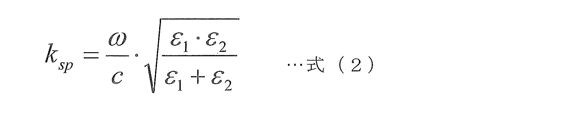
c:光速度
ε1:回折格子428上の媒質(収容部211内の液体)の誘電率=n2
ε2:回折格子428を構成する媒質(金属)の誘電率
次に、検出システム300を用いた被検出物質の検出方法について説明する。図16は、本実施の形態の検出方法を行う際の検出システム300の動作手順の一例を示すフローチャートである。
以上のように、本実施の形態に係る検出チップ400、検出システム300および検出方法によれば、収容部211内の液体の液面を透過させずに蛍光βを検出するため、液面および気泡による検出結果への影響を抑制して、被検出物質を高い信頼性で検出することができる。
非特許文献1:Tawa K., et al., "Zinc Oxide-Coated Plasmonic Chip Modified with a Bispecific Antibody for Sensitive Detection of a Fluorescent Labeled-Antigen", Anal. Chem., Vol. 83, pp. 5944-5948.
上記各実施の形態では、側壁部材220が光学素子としてプリズム221を含む検出チップ200または側壁部材220が光学素子として回折格子428を含む検出チップ400を用いた態様について説明したが、検出チップは、他の光学素子を含んでいてもよい。検出チップが含みうる光学素子の例には、プリズム、微細な凸部または凹部が周期的に配列されている部材(例えば、回折格子やナノホールアレイ、ナノ粒子層など)、光導波路(光ファイバーを含む)、光反射部材が含まれる。光学素子の種類に関わらず、反応場は、直接、または他の部材(例えば金属膜)を介して光学素子の上に配置される。
非特許文献2:De Leebeeck A., et al., "On-Chip Surface-Based Detection with Nanohole Arrays", Anal. Chem., Vol. 79, pp. 4094-4100.
非特許文献3:Kurita M, "Precious Metals for Localized Surface Plasmon Resonance Measurement Applications", J. Surf. Finish. Soc. Jpn., Vol. 62, pp. 306-308.
非特許文献4:Slavik R., et al., "A miniature fiber optic surface plasmon resonance sensor for fast detection of staphylococcal enterotoxin B", Biosensors and
Bioelectronics, Vol. 17, pp. 591-595.
非特許文献5:Tsunoda K., "Waveguide Chemical- and Bio-Sensors Using Evanescent Wave", Kogaku (Japanese Journal of Optics: Publication of the Optical Society of Japan), Vol. 34, pp. 513-517.
非特許文献6:Higashino I., "光導波路センサを用いた小型臨床検査装置用の簡易定量検査技術", Toshiba Review, Vol. 67, pp. 60-61.
非特許文献7:Kurihara Y. et al., "The Promise of Expanding Areas of Application for Reflectometric Interference Spectroscopy", Konica Minolta Technology Report, Vol. 9, pp. 29-35.
110、310 励起光照射ユニット
111 光源ユニット
112 第1角度調整部
120、320 蛍光検出ユニット
121 第1レンズ
122 光学フィルター
123 第2レンズ
124 位置切替部
125 検出部
130 送液ユニット
131 液体チップ
132 ピペット
133 シリンジポンプ
134 ノズルユニット
135 ピペットチップ
136 ピペット制御部
140 加振部
150、350 制御部
200、400 検出チップ
210 ウェル本体
211 収容部
212 第1開口
213 第2開口
214 保持部
220、420 側壁部材
221 プリズム
222 入射面
223 反射面
224 出射面
225、425 金属膜
226、426 反応場
227、427 捕捉領域
230 第2収容部
240 液面
326 第2角度調整部
421 基板
428 回折格子
α 励起光
α’ 励起光の反射光
β 蛍光
γ プラズモン散乱光
Claims (17)
- 上部および側部に開口を有する収容部を含むウェル本体と、
被検出物質を捕捉するための捕捉領域が配置されている側壁部材と、
を有し、
前記側壁部材は、前記収容部の側部の開口を介して前記捕捉領域の少なくとも一部が前記収容部内に露出し、かつ前記側壁部材が前記収容部の側部の開口の少なくとも一部を閉塞するように、前記ウェル本体に固定されている、
検出チップ。 - 前記側壁部材は、光学素子を含む、請求項1に記載の検出チップ。
- 前記光学素子は、プリズム、微細な凸部または凹部が周期的に配列されている部材、光導波路または光反射部材である、請求項2に記載の検出チップ。
- 前記光学素子は、光を入射させるための入射面と、前記入射面で入射した光を反射させるための反射面とを含むプリズムであり、
前記捕捉領域は、前記反射面上に金属膜を介さずにまたは金属膜を介して配置されている、
請求項3に記載の検出チップ。 - 前記側壁部材は、前記反射面上に配置された金属膜を有し、
前記捕捉領域は、前記金属膜上に配置されている、
請求項4に記載の検出チップ。 - 前記ウェル本体の、前記収容部を構成する側壁のうち前記捕捉領域と対向する側壁は、光透過性を有している、請求項1~5のいずれか一項に記載の検出チップ。
- 前記光学素子は、微細な凸部または凹部が周期的に配列されており、かつその表面が金属で被覆されている回折格子であり、
前記回折格子は、前記収容部の側部の開口を介して前記収容部内に露出し、
前記捕捉領域は、前記回折格子上に配置されており、
前記ウェル本体の前記収容部を構成する側壁の少なくとも一部は、光透過性を有している、
請求項3に記載の検出チップ。 - 前記捕捉領域のうちの前記収容部内に露出している領域は、前記収容部の最深部から離れた位置に配置されている、請求項1~7のいずれか一項に記載の検出チップ。
- 前記ウェル本体または前記側壁部材から側方に突出する保持部をさらに有する、請求項1~8のいずれか一項に記載の検出チップ。
- 上部に開口を有する収容部と、前記収容部を構成する側壁の内面上に金属膜を介さずにまたは金属膜を介して配置された、被検出物質を捕捉するための反応場とを有する検出チップと、
前記反応場に対応する位置の前記側壁の内面においてエバネッセント光が生じるように、または前記金属膜において表面プラズモン共鳴が生じるように外部から前記検出チップに光を照射する光源と、
前記光源が前記検出チップに光を照射したときに、前記検出チップから放出される光であって、前記反応場に捕捉されている被検出物質の量に応じて光量が変化する光を検出する検出部と、
を有する、検出システム。 - 前記検出チップは、前記側壁の内面上に配置された金属膜を有し、
前記反応場は、前記金属膜上に配置されており、
前記検出チップの、前記収容部を構成する側壁のうち前記金属膜が配置されている側壁および前記反応場と対向する側壁は、光透過性を有しており、
前記光源は、前記金属膜においてプラズモン共鳴が生じるように、前記金属膜が配置されている側壁の内面に光を照射し、
前記検出部は、前記光源が前記金属膜が配置されている側壁の内面に光を照射したときに、前記反応場に捕捉されている被検出物質を標識する蛍光物質から放出され、かつ前記反応場と対向する側壁を透過した蛍光を検出する、
請求項10に記載の検出システム。 - 前記検出チップは、前記側壁の内面上に配置された、その表面に回折格子が形成されている金属膜を有し、
前記反応場は、前記回折格子上に配置されており、
前記検出チップの前記収容部を構成する側壁の少なくとも一部は、光透過性を有しており、
前記光源は、前記金属膜においてプラズモン共鳴が生じるように、前記回折格子に光を照射し、
前記検出部は、前記光源が前記回折格子に光を照射したときに、前記反応場に捕捉されている被検出物質を標識する蛍光物質から放出され、かつ光透過性を有する前記側壁を透過した蛍光を検出する、
請求項10に記載の検出システム。 - 前記収容部内に収容された液体を撹拌するために前記検出チップを振動させる加振部をさらに有する、請求項10~12のいずれか一項に記載の検出システム。
- 上部に開口を有する収容部と、前記収容部を構成する側壁の内面上に金属膜を介さずにまたは金属膜を介して配置された反応場とを有する検出チップの前記反応場に被検出物質を捕捉させる第1工程と、
前記反応場に対応する位置の前記側壁の内面においてエバネッセント光が生じるように、または前記金属膜において表面プラズモン共鳴が生じるように外部から前記検出チップに光を照射するとともに、前記検出チップから放出される光であって、前記反応場に捕捉されている被検出物質の量に応じて光量が変化する光を検出する第2工程と、
を有する、検出方法。 - 前記検出チップは、前記側壁の内面上に配置された金属膜を有し、
前記反応場は、前記金属膜上に配置されており、
前記検出チップの、前記収容部を構成する側壁のうち前記金属膜が配置されている側壁および前記反応場と対向する側壁は、光透過性を有しており、
前記第1工程では、前記検出チップの前記反応場に被検出物質を捕捉させるとともに、前記反応場に捕捉されている前記被検出物質を蛍光物質で標識し、
前記第2工程では、前記金属膜においてプラズモン共鳴が生じるように、前記金属膜が配置されている側壁の内面に光を照射するとともに、前記反応場に捕捉されている被検出物質を標識する蛍光物質から放出され、かつ前記反応場と対向する側壁を透過した蛍光を検出する、
請求項14に記載の検出方法。 - 前記検出チップは、前記側壁の内面上に配置された、その表面に回折格子が形成されている金属膜を有し、
前記反応場は、前記回折格子上に配置されており、
前記検出チップの前記収容部を構成する側壁の少なくとも一部は、光透過性を有しており、
前記第1工程では、前記検出チップの前記反応場に被検出物質を捕捉させるとともに、前記反応場に捕捉されている前記被検出物質を蛍光物質で標識し、
前記第2工程では、前記金属膜においてプラズモン共鳴が生じるように、前記回折格子に光を照射するとともに、前記反応場に捕捉されている被検出物質を標識する蛍光物質から放出され、かつ光透過性を有する前記側壁を透過した蛍光を検出する、
請求項14に記載の検出方法。 - 前記第1工程において、前記収容部内に液体が収容されている状態で前記検出チップを振動させる、請求項14~16のいずれか一項に記載の検出方法。
Priority Applications (4)
| Application Number | Priority Date | Filing Date | Title |
|---|---|---|---|
| US16/319,046 US11408817B2 (en) | 2016-07-28 | 2017-07-24 | Detection chip, detection system, and detection method |
| JP2018529875A JP6991972B2 (ja) | 2016-07-28 | 2017-07-24 | 検出チップ、検出システムおよび検出方法 |
| ES17834244T ES3055651T3 (en) | 2016-07-28 | 2017-07-24 | Detection chip, detection system, and detection method |
| EP17834244.0A EP3495802B1 (en) | 2016-07-28 | 2017-07-24 | Detection chip, detection system, and detection method |
Applications Claiming Priority (2)
| Application Number | Priority Date | Filing Date | Title |
|---|---|---|---|
| JP2016-148345 | 2016-07-24 | ||
| JP2016148345 | 2016-07-28 |
Publications (1)
| Publication Number | Publication Date |
|---|---|
| WO2018021238A1 true WO2018021238A1 (ja) | 2018-02-01 |
Family
ID=61017085
Family Applications (1)
| Application Number | Title | Priority Date | Filing Date |
|---|---|---|---|
| PCT/JP2017/026684 Ceased WO2018021238A1 (ja) | 2016-07-28 | 2017-07-24 | 検出チップ、検出システムおよび検出方法 |
Country Status (5)
| Country | Link |
|---|---|
| US (1) | US11408817B2 (ja) |
| EP (1) | EP3495802B1 (ja) |
| JP (1) | JP6991972B2 (ja) |
| ES (1) | ES3055651T3 (ja) |
| WO (1) | WO2018021238A1 (ja) |
Cited By (6)
| Publication number | Priority date | Publication date | Assignee | Title |
|---|---|---|---|---|
| WO2018150944A1 (ja) * | 2017-02-15 | 2018-08-23 | コニカミノルタ株式会社 | 検査チップ及び検査システム |
| WO2019221040A1 (ja) * | 2018-05-16 | 2019-11-21 | コニカミノルタ株式会社 | 検体検出チップ及びこれを用いた検体検出装置 |
| WO2019230222A1 (ja) * | 2018-06-01 | 2019-12-05 | コニカミノルタ株式会社 | 表面プラズモン励起増強蛍光測定法 |
| JPWO2018150943A1 (ja) * | 2017-02-15 | 2019-12-12 | コニカミノルタ株式会社 | 送液システム、検査システム及び送液方法 |
| WO2021009995A1 (ja) * | 2019-07-12 | 2021-01-21 | コニカミノルタ株式会社 | 検出装置および検出方法 |
| JPWO2021059859A1 (ja) * | 2019-09-24 | 2021-04-01 |
Families Citing this family (3)
| Publication number | Priority date | Publication date | Assignee | Title |
|---|---|---|---|---|
| WO2019118495A1 (en) * | 2017-12-12 | 2019-06-20 | Board Of Regents, The University Of Texas System | Nanosensors and methods of making and using nanosensors |
| JP7322593B2 (ja) * | 2019-08-23 | 2023-08-08 | 株式会社サタケ | 微生物の検査装置及びその方法 |
| CN118258448B (zh) * | 2024-05-29 | 2025-02-18 | 深圳市中科鑫维电子科技有限公司 | 一种芯片测试方法及芯片测试设备 |
Citations (9)
| Publication number | Priority date | Publication date | Assignee | Title |
|---|---|---|---|---|
| JP2002513936A (ja) * | 1998-05-01 | 2002-05-14 | ジェン−プロウブ インコーポレイテッド | 自動化診断用分析器および方法 |
| JP2004500571A (ja) * | 2000-03-14 | 2004-01-08 | スプリング、システムズ、アクチボラグ | 改良された撮像型表面プラズモン共鳴装置 |
| JP2006090758A (ja) * | 2004-09-21 | 2006-04-06 | Fuji Photo Film Co Ltd | 全反射減衰を利用した測定装置 |
| US20080131939A1 (en) * | 2006-05-30 | 2008-06-05 | Roper D Keith | Simultaneous amplification and detection of ribonucleic acid be an optical method using surface plasmon resonance |
| WO2012157403A1 (ja) | 2011-05-19 | 2012-11-22 | コニカミノルタホールディングス株式会社 | 表面プラズモン励起増強蛍光測定装置およびこれを用いた蛍光検出方法 |
| WO2015068813A1 (ja) * | 2013-11-07 | 2015-05-14 | コニカミノルタ株式会社 | チップおよび表面プラズモン増強蛍光測定方法 |
| JP2015111063A (ja) * | 2013-12-06 | 2015-06-18 | コニカミノルタ株式会社 | 表面プラズモン増強蛍光測定方法および表面プラズモン増強蛍光測定装置 |
| JP2016121936A (ja) * | 2014-12-25 | 2016-07-07 | 株式会社島津製作所 | ガス成分測定装置 |
| JP2016148345A (ja) | 2012-05-10 | 2016-08-18 | エムエーエヌ・ディーゼル・アンド・ターボ・フィリアル・アフ・エムエーエヌ・ディーゼル・アンド・ターボ・エスイー・ティスクランド | 燃焼機関 |
Family Cites Families (10)
| Publication number | Priority date | Publication date | Assignee | Title |
|---|---|---|---|---|
| US4833087A (en) * | 1987-02-27 | 1989-05-23 | Eastman Kodak Company | Disposable container configured to produce uniform signal |
| AU760704B2 (en) | 1998-05-25 | 2003-05-22 | Herbert Peter Jennissen | Flow-through shear analyzer for biologically active molecules in liquid layers on surfaces |
| WO2003023400A2 (en) | 2001-09-13 | 2003-03-20 | Axela Biosensors Inc. | Method and apparatus for assay based on light diffraction |
| JP4098603B2 (ja) * | 2002-11-11 | 2008-06-11 | 東亜ディーケーケー株式会社 | 光学センサ |
| US20160355869A1 (en) * | 2005-08-02 | 2016-12-08 | University Of Utah Research Foundation | Biosensors including metallic nanocavities |
| JP2007047004A (ja) | 2005-08-09 | 2007-02-22 | Olympus Corp | 反応容器とこの反応容器を用いた分析装置 |
| EP2645085A4 (en) * | 2010-11-26 | 2015-07-22 | Konica Minolta Inc | PRISM FILE FOR AN ANALYSIS CHIP, ANALYSIS CHIP WITH THE PRISM FILE AND PROCESS FOR PREPARING THE PRISM FILE FOR AN ANALYSIS CHIP |
| JP5865713B2 (ja) * | 2012-01-20 | 2016-02-17 | 株式会社東芝 | 自動分析装置 |
| EP3187874B1 (en) * | 2014-08-25 | 2020-09-30 | Konica Minolta, Inc. | Detection method and detection device |
| JP6627778B2 (ja) * | 2014-12-09 | 2020-01-08 | コニカミノルタ株式会社 | 検出装置および検出方法 |
-
2017
- 2017-07-24 JP JP2018529875A patent/JP6991972B2/ja active Active
- 2017-07-24 US US16/319,046 patent/US11408817B2/en active Active
- 2017-07-24 EP EP17834244.0A patent/EP3495802B1/en active Active
- 2017-07-24 ES ES17834244T patent/ES3055651T3/es active Active
- 2017-07-24 WO PCT/JP2017/026684 patent/WO2018021238A1/ja not_active Ceased
Patent Citations (9)
| Publication number | Priority date | Publication date | Assignee | Title |
|---|---|---|---|---|
| JP2002513936A (ja) * | 1998-05-01 | 2002-05-14 | ジェン−プロウブ インコーポレイテッド | 自動化診断用分析器および方法 |
| JP2004500571A (ja) * | 2000-03-14 | 2004-01-08 | スプリング、システムズ、アクチボラグ | 改良された撮像型表面プラズモン共鳴装置 |
| JP2006090758A (ja) * | 2004-09-21 | 2006-04-06 | Fuji Photo Film Co Ltd | 全反射減衰を利用した測定装置 |
| US20080131939A1 (en) * | 2006-05-30 | 2008-06-05 | Roper D Keith | Simultaneous amplification and detection of ribonucleic acid be an optical method using surface plasmon resonance |
| WO2012157403A1 (ja) | 2011-05-19 | 2012-11-22 | コニカミノルタホールディングス株式会社 | 表面プラズモン励起増強蛍光測定装置およびこれを用いた蛍光検出方法 |
| JP2016148345A (ja) | 2012-05-10 | 2016-08-18 | エムエーエヌ・ディーゼル・アンド・ターボ・フィリアル・アフ・エムエーエヌ・ディーゼル・アンド・ターボ・エスイー・ティスクランド | 燃焼機関 |
| WO2015068813A1 (ja) * | 2013-11-07 | 2015-05-14 | コニカミノルタ株式会社 | チップおよび表面プラズモン増強蛍光測定方法 |
| JP2015111063A (ja) * | 2013-12-06 | 2015-06-18 | コニカミノルタ株式会社 | 表面プラズモン増強蛍光測定方法および表面プラズモン増強蛍光測定装置 |
| JP2016121936A (ja) * | 2014-12-25 | 2016-07-07 | 株式会社島津製作所 | ガス成分測定装置 |
Non-Patent Citations (8)
| Title |
|---|
| DE LEEBEECK A. ET AL.: "On-Chip Surface-Based Detection with Nanohole Arrays", ANAL. CHEM., vol. 79, pages 4094 - 4100, XP002560502, DOI: doi:10.1021/ac070001a |
| HIGASHINO I.: "Simple Quantitative Test Technique for Small Clinical Tester Using Optical Waveguide Sensor", TOSHIBA REVIEW, vol. 67, pages 60 - 61 |
| KURIHARA Y ET AL.: "The Promise of Expanding Areas of Application for Reflectometric Interference Spectroscopy", KONICA MINOLTA TECHNOLOGY REPORT, vol. 9, pages 29 - 35 |
| KURITA M: "Precious Metals for Localized Surface Plasmon Resonance Measurement Applications", J. SURF. FINISH. SOC. JPN., vol. 62, pages 306 - 308 |
| See also references of EP3495802A4 |
| SLAVIK R. ET AL.: "A miniature fiber optic surface plasmon resonance sensor for fast detection of staphylococcal enterotoxin B", BIOSENSORS AND BIOELECTRONICS, vol. 17, pages 591 - 595 |
| TAWA K. ET AL.: "Zinc Oxide-Coated Plasmonic Chip Modified with a Bispecific Antibody for Sensitive Detection of a Fluorescent Labeled-Antigen", ANAL. CHEM., vol. 83, pages 5944 - 5948 |
| TSUNODA K: "Waveguide Chemical- and Bio-Sensors Using Evanescent Wave", KOGAKU (JAPANESE JOURNAL OF OPTICS: PUBLICATION OF THE OPTICAL SOCIETY OF JAPAN, vol. 34, pages 513 - 517 |
Cited By (13)
| Publication number | Priority date | Publication date | Assignee | Title |
|---|---|---|---|---|
| WO2018150944A1 (ja) * | 2017-02-15 | 2018-08-23 | コニカミノルタ株式会社 | 検査チップ及び検査システム |
| JPWO2018150944A1 (ja) * | 2017-02-15 | 2019-12-12 | コニカミノルタ株式会社 | 検査チップ及び検査システム |
| JPWO2018150943A1 (ja) * | 2017-02-15 | 2019-12-12 | コニカミノルタ株式会社 | 送液システム、検査システム及び送液方法 |
| US11224879B2 (en) | 2017-02-15 | 2022-01-18 | Konica Minolta, Inc. | Inspection chip and inspection system |
| WO2019221040A1 (ja) * | 2018-05-16 | 2019-11-21 | コニカミノルタ株式会社 | 検体検出チップ及びこれを用いた検体検出装置 |
| WO2019230222A1 (ja) * | 2018-06-01 | 2019-12-05 | コニカミノルタ株式会社 | 表面プラズモン励起増強蛍光測定法 |
| JPWO2021009995A1 (ja) * | 2019-07-12 | 2021-01-21 | ||
| WO2021009995A1 (ja) * | 2019-07-12 | 2021-01-21 | コニカミノルタ株式会社 | 検出装置および検出方法 |
| JP7556854B2 (ja) | 2019-07-12 | 2024-09-26 | 大塚製薬株式会社 | 検出装置および検出方法 |
| US12196674B2 (en) | 2019-07-12 | 2025-01-14 | Otsuka Pharmaceutical Co., Ltd. | Detection device and detection method |
| JPWO2021059859A1 (ja) * | 2019-09-24 | 2021-04-01 | ||
| EP4036555A4 (en) * | 2019-09-24 | 2023-08-23 | Otsuka Pharmaceutical Co., Ltd. | DETECTION METHOD AND DETECTION DEVICE |
| JP7482887B2 (ja) | 2019-09-24 | 2024-05-14 | 大塚製薬株式会社 | 検出方法および検出装置 |
Also Published As
| Publication number | Publication date |
|---|---|
| EP3495802B1 (en) | 2025-11-05 |
| US11408817B2 (en) | 2022-08-09 |
| ES3055651T3 (en) | 2026-02-13 |
| JP6991972B2 (ja) | 2022-01-13 |
| JPWO2018021238A1 (ja) | 2019-05-16 |
| EP3495802A4 (en) | 2019-10-30 |
| EP3495802A1 (en) | 2019-06-12 |
| US20210356386A1 (en) | 2021-11-18 |
Similar Documents
| Publication | Publication Date | Title |
|---|---|---|
| JP6991972B2 (ja) | 検出チップ、検出システムおよび検出方法 | |
| JP6565934B2 (ja) | 表面プラズモン増強蛍光測定装置および表面プラズモン増強蛍光測定方法 | |
| JP6801656B2 (ja) | 検出装置および検出方法 | |
| WO2017082089A1 (ja) | 表面プラズモン共鳴蛍光分析方法および表面プラズモン共鳴蛍光分析装置 | |
| JP6888548B2 (ja) | 測定方法 | |
| JP6838612B2 (ja) | 検査チップ及び検査システム | |
| JPWO2017057136A1 (ja) | 表面プラズモン励起増強蛍光分光測定方法、および測定用キット | |
| JP2015111063A (ja) | 表面プラズモン増強蛍光測定方法および表面プラズモン増強蛍光測定装置 | |
| JPWO2019230222A1 (ja) | 表面プラズモン励起増強蛍光測定法 | |
| WO2016093039A1 (ja) | 検出チップおよび検出方法 | |
| JP6627778B2 (ja) | 検出装置および検出方法 | |
| WO2019221040A1 (ja) | 検体検出チップ及びこれを用いた検体検出装置 | |
| EP4036555B1 (en) | Detection method and detection device | |
| WO2018150943A1 (ja) | 送液システム、検査システム及び送液方法 | |
| JP6586884B2 (ja) | チップおよび表面プラズモン増強蛍光測定方法 | |
| JP6711285B2 (ja) | 検出方法、検出装置およびチップ | |
| WO2016203832A1 (ja) | 検出チップ、検出方法、検出装置および検出システム |
Legal Events
| Date | Code | Title | Description |
|---|---|---|---|
| 121 | Ep: the epo has been informed by wipo that ep was designated in this application |
Ref document number: 17834244 Country of ref document: EP Kind code of ref document: A1 |
|
| ENP | Entry into the national phase |
Ref document number: 2018529875 Country of ref document: JP Kind code of ref document: A |
|
| NENP | Non-entry into the national phase |
Ref country code: DE |
|
| ENP | Entry into the national phase |
Ref document number: 2017834244 Country of ref document: EP Effective date: 20190228 |
|
| WWG | Wipo information: grant in national office |
Ref document number: 2017834244 Country of ref document: EP |