WO2018021534A1 - 電力変換装置 - Google Patents
電力変換装置 Download PDFInfo
- Publication number
- WO2018021534A1 WO2018021534A1 PCT/JP2017/027453 JP2017027453W WO2018021534A1 WO 2018021534 A1 WO2018021534 A1 WO 2018021534A1 JP 2017027453 W JP2017027453 W JP 2017027453W WO 2018021534 A1 WO2018021534 A1 WO 2018021534A1
- Authority
- WO
- WIPO (PCT)
- Prior art keywords
- converters
- converter
- output current
- switching operation
- phase
- Prior art date
- Legal status (The legal status is an assumption and is not a legal conclusion. Google has not performed a legal analysis and makes no representation as to the accuracy of the status listed.)
- Ceased
Links
Images



Classifications
-
- H—ELECTRICITY
- H02—GENERATION; CONVERSION OR DISTRIBUTION OF ELECTRIC POWER
- H02J—ELECTRIC POWER NETWORKS; CIRCUIT ARRANGEMENTS OR SYSTEMS FOR SUPPLYING OR DISTRIBUTING ELECTRIC POWER; SYSTEMS FOR STORING ELECTRIC ENERGY
- H02J1/00—Circuit arrangements for DC mains or DC distribution networks
- H02J1/10—Parallel operation of DC sources
- H02J1/102—Parallel operation of DC sources being switching converters
-
- H—ELECTRICITY
- H02—GENERATION; CONVERSION OR DISTRIBUTION OF ELECTRIC POWER
- H02J—ELECTRIC POWER NETWORKS; CIRCUIT ARRANGEMENTS OR SYSTEMS FOR SUPPLYING OR DISTRIBUTING ELECTRIC POWER; SYSTEMS FOR STORING ELECTRIC ENERGY
- H02J1/00—Circuit arrangements for DC mains or DC distribution networks
- H02J1/10—Parallel operation of DC sources
- H02J1/106—Parallel operation of DC sources for load balancing, symmetrisation, or sharing
-
- H—ELECTRICITY
- H02—GENERATION; CONVERSION OR DISTRIBUTION OF ELECTRIC POWER
- H02J—ELECTRIC POWER NETWORKS; CIRCUIT ARRANGEMENTS OR SYSTEMS FOR SUPPLYING OR DISTRIBUTING ELECTRIC POWER; SYSTEMS FOR STORING ELECTRIC ENERGY
- H02J3/00—Circuit arrangements for AC mains or AC distribution networks
- H02J3/38—Arrangements for feeding a single network from two or more generators or sources in parallel; Arrangements for feeding already energised networks from additional generators or sources in parallel
-
- H—ELECTRICITY
- H02—GENERATION; CONVERSION OR DISTRIBUTION OF ELECTRIC POWER
- H02M—APPARATUS FOR CONVERSION BETWEEN AC AND AC, BETWEEN AC AND DC, OR BETWEEN DC AND DC, AND FOR USE WITH MAINS OR SIMILAR POWER SUPPLY SYSTEMS; CONVERSION OF DC OR AC INPUT POWER INTO SURGE OUTPUT POWER; CONTROL OR REGULATION THEREOF
- H02M1/00—Details of apparatus for conversion
- H02M1/14—Arrangements for reducing ripples from DC input or output
-
- H—ELECTRICITY
- H02—GENERATION; CONVERSION OR DISTRIBUTION OF ELECTRIC POWER
- H02M—APPARATUS FOR CONVERSION BETWEEN AC AND AC, BETWEEN AC AND DC, OR BETWEEN DC AND DC, AND FOR USE WITH MAINS OR SIMILAR POWER SUPPLY SYSTEMS; CONVERSION OF DC OR AC INPUT POWER INTO SURGE OUTPUT POWER; CONTROL OR REGULATION THEREOF
- H02M1/00—Details of apparatus for conversion
- H02M1/14—Arrangements for reducing ripples from DC input or output
- H02M1/143—Arrangements for reducing ripples from DC input or output using compensating arrangements
-
- H—ELECTRICITY
- H02—GENERATION; CONVERSION OR DISTRIBUTION OF ELECTRIC POWER
- H02M—APPARATUS FOR CONVERSION BETWEEN AC AND AC, BETWEEN AC AND DC, OR BETWEEN DC AND DC, AND FOR USE WITH MAINS OR SIMILAR POWER SUPPLY SYSTEMS; CONVERSION OF DC OR AC INPUT POWER INTO SURGE OUTPUT POWER; CONTROL OR REGULATION THEREOF
- H02M3/00—Conversion of DC power input into DC power output
-
- H—ELECTRICITY
- H02—GENERATION; CONVERSION OR DISTRIBUTION OF ELECTRIC POWER
- H02M—APPARATUS FOR CONVERSION BETWEEN AC AND AC, BETWEEN AC AND DC, OR BETWEEN DC AND DC, AND FOR USE WITH MAINS OR SIMILAR POWER SUPPLY SYSTEMS; CONVERSION OF DC OR AC INPUT POWER INTO SURGE OUTPUT POWER; CONTROL OR REGULATION THEREOF
- H02M3/00—Conversion of DC power input into DC power output
- H02M3/02—Conversion of DC power input into DC power output without intermediate conversion into AC
- H02M3/04—Conversion of DC power input into DC power output without intermediate conversion into AC by static converters
-
- H—ELECTRICITY
- H02—GENERATION; CONVERSION OR DISTRIBUTION OF ELECTRIC POWER
- H02M—APPARATUS FOR CONVERSION BETWEEN AC AND AC, BETWEEN AC AND DC, OR BETWEEN DC AND DC, AND FOR USE WITH MAINS OR SIMILAR POWER SUPPLY SYSTEMS; CONVERSION OF DC OR AC INPUT POWER INTO SURGE OUTPUT POWER; CONTROL OR REGULATION THEREOF
- H02M3/00—Conversion of DC power input into DC power output
- H02M3/02—Conversion of DC power input into DC power output without intermediate conversion into AC
- H02M3/04—Conversion of DC power input into DC power output without intermediate conversion into AC by static converters
- H02M3/10—Conversion of DC power input into DC power output without intermediate conversion into AC by static converters using discharge tubes with control electrode or semiconductor devices with control electrode
- H02M3/145—Conversion of DC power input into DC power output without intermediate conversion into AC by static converters using discharge tubes with control electrode or semiconductor devices with control electrode using devices of a triode or transistor type requiring continuous application of a control signal
- H02M3/155—Conversion of DC power input into DC power output without intermediate conversion into AC by static converters using discharge tubes with control electrode or semiconductor devices with control electrode using devices of a triode or transistor type requiring continuous application of a control signal using semiconductor devices only
-
- H—ELECTRICITY
- H02—GENERATION; CONVERSION OR DISTRIBUTION OF ELECTRIC POWER
- H02M—APPARATUS FOR CONVERSION BETWEEN AC AND AC, BETWEEN AC AND DC, OR BETWEEN DC AND DC, AND FOR USE WITH MAINS OR SIMILAR POWER SUPPLY SYSTEMS; CONVERSION OF DC OR AC INPUT POWER INTO SURGE OUTPUT POWER; CONTROL OR REGULATION THEREOF
- H02M7/00—Conversion of AC power input into DC power output; Conversion of DC power input into AC power output
- H02M7/42—Conversion of DC power input into AC power output without possibility of reversal
- H02M7/44—Conversion of DC power input into AC power output without possibility of reversal by static converters
- H02M7/48—Conversion of DC power input into AC power output without possibility of reversal by static converters using discharge tubes with control electrode or semiconductor devices with control electrode
-
- H—ELECTRICITY
- H02—GENERATION; CONVERSION OR DISTRIBUTION OF ELECTRIC POWER
- H02J—ELECTRIC POWER NETWORKS; CIRCUIT ARRANGEMENTS OR SYSTEMS FOR SUPPLYING OR DISTRIBUTING ELECTRIC POWER; SYSTEMS FOR STORING ELECTRIC ENERGY
- H02J1/00—Circuit arrangements for DC mains or DC distribution networks
- H02J1/10—Parallel operation of DC sources
-
- H—ELECTRICITY
- H02—GENERATION; CONVERSION OR DISTRIBUTION OF ELECTRIC POWER
- H02M—APPARATUS FOR CONVERSION BETWEEN AC AND AC, BETWEEN AC AND DC, OR BETWEEN DC AND DC, AND FOR USE WITH MAINS OR SIMILAR POWER SUPPLY SYSTEMS; CONVERSION OF DC OR AC INPUT POWER INTO SURGE OUTPUT POWER; CONTROL OR REGULATION THEREOF
- H02M3/00—Conversion of DC power input into DC power output
- H02M3/02—Conversion of DC power input into DC power output without intermediate conversion into AC
- H02M3/04—Conversion of DC power input into DC power output without intermediate conversion into AC by static converters
- H02M3/10—Conversion of DC power input into DC power output without intermediate conversion into AC by static converters using discharge tubes with control electrode or semiconductor devices with control electrode
- H02M3/145—Conversion of DC power input into DC power output without intermediate conversion into AC by static converters using discharge tubes with control electrode or semiconductor devices with control electrode using devices of a triode or transistor type requiring continuous application of a control signal
- H02M3/155—Conversion of DC power input into DC power output without intermediate conversion into AC by static converters using discharge tubes with control electrode or semiconductor devices with control electrode using devices of a triode or transistor type requiring continuous application of a control signal using semiconductor devices only
- H02M3/156—Conversion of DC power input into DC power output without intermediate conversion into AC by static converters using discharge tubes with control electrode or semiconductor devices with control electrode using devices of a triode or transistor type requiring continuous application of a control signal using semiconductor devices only with automatic control of output voltage or current, e.g. switching regulators
- H02M3/158—Conversion of DC power input into DC power output without intermediate conversion into AC by static converters using discharge tubes with control electrode or semiconductor devices with control electrode using devices of a triode or transistor type requiring continuous application of a control signal using semiconductor devices only with automatic control of output voltage or current, e.g. switching regulators including plural semiconductor devices as final control devices for a single load
- H02M3/1584—Conversion of DC power input into DC power output without intermediate conversion into AC by static converters using discharge tubes with control electrode or semiconductor devices with control electrode using devices of a triode or transistor type requiring continuous application of a control signal using semiconductor devices only with automatic control of output voltage or current, e.g. switching regulators including plural semiconductor devices as final control devices for a single load with a plurality of power processing stages connected in parallel
- H02M3/1586—Conversion of DC power input into DC power output without intermediate conversion into AC by static converters using discharge tubes with control electrode or semiconductor devices with control electrode using devices of a triode or transistor type requiring continuous application of a control signal using semiconductor devices only with automatic control of output voltage or current, e.g. switching regulators including plural semiconductor devices as final control devices for a single load with a plurality of power processing stages connected in parallel switched with a phase shift, i.e. interleaved
-
- Y—GENERAL TAGGING OF NEW TECHNOLOGICAL DEVELOPMENTS; GENERAL TAGGING OF CROSS-SECTIONAL TECHNOLOGIES SPANNING OVER SEVERAL SECTIONS OF THE IPC; TECHNICAL SUBJECTS COVERED BY FORMER USPC CROSS-REFERENCE ART COLLECTIONS [XRACs] AND DIGESTS
- Y02—TECHNOLOGIES OR APPLICATIONS FOR MITIGATION OR ADAPTATION AGAINST CLIMATE CHANGE
- Y02E—REDUCTION OF GREENHOUSE GAS [GHG] EMISSIONS, RELATED TO ENERGY GENERATION, TRANSMISSION OR DISTRIBUTION
- Y02E10/00—Energy generation through renewable energy sources
- Y02E10/50—Photovoltaic [PV] energy
- Y02E10/56—Power conversion systems, e.g. maximum power point trackers
Definitions
- the present invention relates to a power conversion device including a plurality of DC / DC converters for supplying power to a common DC bus.
- a power conversion device including a plurality of DC / DC converters that supply power to a common DC bus is known (see, for example, Patent Document 1).
- the timing of the switching operation of each DC / DC converter is different. Therefore, compared with the case where a plurality of DC / DC converters are simultaneously switched, the amount of fluctuation in the output current of the DC bus can be reduced, and the smoothing capacitor provided in the DC bus can be reduced in size.
- the present invention has been made in view of such a situation, and an object thereof is to provide a power conversion device capable of smoothing an output current more appropriately.
- a power conversion device converts the output voltage of each corresponding DC power source into a voltage having a different value by a switching operation, and the converted voltage is a common DC bus.
- a plurality of DC / DC converters that output to each other and a control unit that causes the plurality of DC / DC converters to perform switching operations at different phases.
- the control unit resets the phase according to the operating states of the plurality of DC power supplies and the plurality of DC / DC converters.
- the output current can be smoothed more appropriately.
- FIG. 3A is a waveform diagram showing the output current of the power conversion device of FIG. 1
- FIG. 3B is a waveform diagram showing the output current corresponding to FIG. It is a figure for demonstrating operation
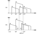
- 6A is a waveform diagram showing an output current before resetting the phase of the power converter of FIG. 5
- FIG. 6B is an output after resetting the phase of the power converter of FIG. It is a wave form diagram which shows an electric current.
- FIG.7 (a) is a wave form diagram which shows a drive signal when the output current of the power converter device which concerns on 3rd Embodiment is normal
- FIG.7 (b) is the output current of the power converter device of FIG.
- FIG. 7C is a waveform diagram illustrating the drive signal when the output current of the power conversion device according to the third embodiment is abnormal.
- FIG. 1 is a diagram illustrating a configuration of a power conversion device 1 according to the first embodiment.
- the power converter 1 includes a plurality of solar cells (DC power supplies) 10-1 to 10-4, a plurality of DC / DC converters 20-1 to 20-4 connected in parallel, a DC bus 30, and a capacitor C1.
- the control part 40 is provided.
- the power conversion device 1 is a multi-string type including a plurality of systems of solar cells 10-1 to 10-4.
- Each of the solar cells 10-1 to 10-4 is a solar cell string in which a plurality of solar cell panels connected in series are grouped. Assume that the numbers of solar cell panels 10-1 to 10-4 connected in series are equal.
- an example in which four solar cells 10-1 to 10-4 and four DC / DC converters 20-1 to 20-4 are provided will be described, but the number is not particularly limited.
- the input terminals of the DC / DC converters 20-1 to 20-4 are connected to the corresponding solar cells 10-1 to 10-4.
- the output terminals of the DC / DC converters 20-1 to 20-4 are connected to the DC bus 30 in common.
- the DC / DC converters 20-1 to 20-4 are, for example, chopper circuits, and convert the output voltages of the corresponding solar cells 10-1 to 10-4 into different direct-current voltages by switching operations, respectively.
- the converted DC voltage is output to the common DC bus 30.
- the voltage of the DC bus 30 is the bus voltage Vbus.
- An output current Io that is the sum of the output currents I1 to I4 of the DC / DC converters 20-1 to 20-4 flows through the DC bus 30.
- the capacitor C1 has one end connected to the DC bus 30 and the other end grounded. Capacitor C1 smoothes output current Io and bus voltage Vbus.
- the DC bus 30 is further connected to a load such as an inverter (not shown).
- the control unit 40 supplies drive signals S1 to S4 which are PWM (Pulse Width Modulaion) signals to the DC / DC converters 20-1 to 20-4, and the DC / DC converters 20-1 to 20-4. 20-4 is controlled. Specifically, the control unit 40 performs PWM control of the DC / DC converter 20-1 by the drive signal S1 so that the bus voltage Vbus approaches the target voltage. Similarly, the control unit 40 individually performs PWM control on the DC / DC converters 20-2 to 20-4.
- PWM Pulse Width Modulaion
- the control unit 40 switches the DC / DC converters 20-1 to 20-4 at different phases using the drive signals S1 to S4 having different phases.
- the total number (n) of the DC / DC converters 20-1 to 20-4 may be preset in the control unit 40 at the time of factory shipment, or may be set by the operator or the like when the power conversion device 1 is installed. May be set.
- the control unit 40 resets the phase according to the operating states of the solar cells 10-1 to 10-4 and the DC / DC converters 20-1 to 20-4. This resetting will be described later.
- the configuration of the control unit 40 can be realized by cooperation of hardware resources and software resources, or only by hardware resources.
- hardware resources analog elements, microcomputers, DSPs, ROMs, RAMs, FPGAs, and other LSIs can be used.
- Firmware and other programs can be used as software resources.
- FIG. 2 is a waveform diagram showing the drive signals S1 to S4 in FIG.
- the phases of the drive signals S1 to S4 are 0 °, 90 °, 180 °, and 270 °, respectively. That is, the phase difference between the drive signal S1 and the drive signal S2, the phase difference between the drive signal S2 and the drive signal S3, the phase difference between the drive signal S3 and the drive signal S4, and the phase difference between the drive signal S4 and the drive signal S1 are respectively 90 °.
- FIG. 3A is a waveform diagram showing the output currents I1 to I4 of the power conversion device 1 in FIG. 1, and FIG. 3B is a waveform diagram showing the output current Io corresponding to FIG. 3A. is there.
- the output currents I1 to I4 flow based on the switching operation of the DC / DC converters 20-1 to 20-4, respectively, and have ripples.
- the phase of the output current I1 is equal to the phase of the drive signal S1 and is 0 °.
- the phase of the output current I2 is equal to the phase of the drive signal S2, and is 90 °.
- the phase of the output current I3 is equal to the phase of the drive signal S3 and is 180 °.
- the phase of the output current I4 is equal to the phase of the drive signal S4 and is 270 °.
- the ripple is averaged at the output current Io which is the sum of the output currents I1 to I4.
- the fluctuation amount of the output current Io is as shown in FIG. It becomes larger than the fluctuation amount. Therefore, in FIG. 3B of the present embodiment, the fluctuation amount of the output current Io can be reduced as compared with the case where the DC / DC converters 20-1 to 20-4 are simultaneously switched, and as a result, the capacitor C1 can be reduced in size and capacity.
- control unit 40 resets the phase when the operating states of the solar cells 10-1 to 10-4 and the DC / DC converters 20-1 to 20-4 change from the initial state.
- FIG. 4 is a diagram for explaining an operation of the power conversion device 1 when a solar cell is not connected.
- the solar cell 10-4 of FIG. 1 is removed.
- the output current I4 of the DC / DC converter 20-4 to which no solar cell is connected is zero. That is, the output current I4 becomes abnormal.
- the timing at which the ripple does not appear in the output current Io periodically exists, and therefore the ripple is biased in time. Therefore, the output current Io is not smoothed as it is.
- the control unit 40 resets the phase by excluding the DC / DC converter 20-4 to which the solar cell is not connected, that is, the DC / DC converter 20-4 having an abnormal output current I4.
- a switch (not shown) in the connection box between the solar cell and the DC / DC converter 20-4 is opened.
- the control unit 40 monitors the state of this switch and determines the DC / DC converter 20-4 to which the open switch is connected as the DC / DC converter 20-4 to which no solar cell is connected. .
- the control unit 40 determines the DC / DC converter 20-4 to which no solar cell is connected based on the input voltage, input current, or output current I1 to I4 of the DC / DC converters 20-1 to 20-4. May be.
- the control unit 40 obtains the number (n ⁇ k) obtained by subtracting the number (k) of the DC / DC converters 20-4 whose output current I4 is abnormal from the total number (n) of the DC / DC converters 20-1 to 20-4. Reset the phase accordingly. Further, the control unit 40 causes the DC / DC converters 20-1 to 20-3 other than the DC / DC converter 20-4 having an abnormal output current I4 to perform switching operation with the reset phase, and the output current I4 is abnormal. The DC / DC converter 20-4 is not switched. The control unit 40 resets the phases of the drive signals S1 to S3 so that the phase difference becomes 360 ° / (nk).
- Example 2 When DC / DC converter fails The control unit 40 resets the phase by excluding the failed DC / DC converter, that is, the DC / DC converter with an abnormal output current.
- the method for resetting the phase is the same as in the above [Example 1].
- the control unit 40 can determine the DC / DC converter that has failed based on the output currents I1 to I4 of the DC / DC converters 20-1 to 20-4.
- Example 3 When the power generation of a solar cell is stopped When the solar cells 10-1 to 10-4 are installed at separate locations, the power generation of one solar cell may be stopped due to sunset or solar radiation fluctuations. is there. Therefore, the control unit 40 excludes the DC / DC converter connected to the solar cell whose power generation has stopped, that is, the DC / DC converter with an abnormal output current, and resets the phase. The method for resetting the phase is the same as in the above [Example 1]. The control unit 40 can determine the solar cell in which power generation has stopped based on the input voltage, input current, or output current I1 to I4 of the DC / DC converters 20-1 to 20-4.
- control unit 40 resets the phase by excluding the DC / DC converter connected to the solar cell whose output voltage is equal to or higher than the bus voltage Vbus, that is, the DC / DC converter whose output current is substantially constant.
- the method for resetting the phase is the same as in the above [Example 1]. In the case of [Example 2] to [Example 4], the same effect as in [Example 1] can be obtained.
- the phase is reset according to the operating states of the solar cells 10-1 to 10-4 and the DC / DC converters 20-1 to 20-4. Therefore, even when the operating states of the solar cells 10-1 to 10-4 and the DC / DC converters 20-1 to 20-4 change and the ripple of the output current Io is uneven in time, The ripple of the output current Io can be dispersed over time. Therefore, the output current Io can be smoothed more appropriately in accordance with various operating states.
- the second embodiment is different from the first embodiment in that the phase is reset when the number of solar cell panels of the solar cell is increased. Below, it demonstrates centering around difference with 1st Embodiment.
- FIG. 5 is a diagram illustrating a configuration of the power conversion device 1A according to the second embodiment.
- the number of solar cell panels connected in series with the solar cells 10-2 is larger than that in FIG.
- the number of solar cell panels of the solar cell 10-2 is large. Is expensive. Therefore, the input current and output current I2 of the DC / DC converter 20-2 are larger than the input current and output currents I1, I3, and I4 of the DC / DC converters 20-1, 20-3, and 20-4.
- the control unit 40A can determine the solar cell 10-2 having an increased number of solar cell panels based on the input voltage, the input current, or the output currents I1 to I4 of the DC / DC converters 20-1 to 20-4.
- the solar cell 10-2 having an increased number of solar cell panels may be set in the control unit 40A by an operator or the like when the solar cell is replaced.
- control unit 40A resets the phase according to the operating states of the solar cells 10-1 to 10-4 and the DC / DC converters 20-1 to 20-4.
- the control unit 40A has a switching operation of the DC / DC converter in which the input current supplied from the corresponding solar cell is larger than a predetermined reference value, and the timing of the switching operation is temporally adjacent to the timing of the switching operation.
- the phase is reset so that the phase difference from the switching operation of the DC / DC converter is larger than the initial value.
- the reference value can be appropriately set by experiment or the like.
- FIG. 6A is a waveform diagram showing the output currents I1 to I4 before the phase of the power conversion device 1A of FIG. 5 is reset
- FIG. 6B is the phase diagram of the power conversion device 1A of FIG.
- FIG. 6 is a waveform diagram showing output currents I1 to I4 after resetting.
- the output current I2 is larger than the other output currents I1, I3, and I4, but the phases of the output currents I1 to I4 are set equally.
- the input current of the DC / DC converter 20-2 is larger than the reference value.
- the timing of the switching operation of the DC / DC converter 20-1 and the timing of the switching operation of the DC / DC converter 20-3 are temporally adjacent to the timing of the switching operation of the DC / DC converter 20-2.
- the control unit 40A makes the phase of the switching operation of the DC / DC converter 20-1 immediately before the switching operation of the DC / DC converter 20-2 whose input current is larger than the reference value smaller than the initial value of 0 ° ( Reset to 0- ⁇ ) °. Further, the control unit 40A makes the phase of the switching operation of the DC / DC converter 20-3 after the switching operation of the DC / DC converter 20-2 whose input current is larger than the reference value larger than the initial value of 180 °, Reset to (180 + ⁇ ) °.
- ⁇ may be a fixed value or may be changed according to the difference between the output currents I1 to I4. The optimum value of ⁇ can be determined as appropriate by experiments or the like.
- phase difference between the switching operation of the DC / DC converter 20-2 and the switching operation of the DC / DC converters 20-1 and 20-3 in which the timing of the switching operation is temporally adjacent to the timing of the switching operation. Is reset to (90 + ⁇ ) ° greater than the initial value of 90 °.
- the overlapping period of the period in which the output current I2 flows and the period in which the output current I1 flows are the same as in the case of FIG. It is shorter.
- the overlapping period of the period in which the output current I2 flows and the period in which the output current I3 flows are also shorter than in the case of FIG.
- the output current Io becomes maximum, but since the overlap period is shortened by resetting the phase as compared with the case of FIG. 6A, the period in which the output current Io is maximum is shortened. Therefore, the output current Io can be further smoothed by resetting the phase.
- the control unit 40A resets only the phase difference between the switching operation of the DC / DC converter 20-2 and the switching operation of the DC / DC converter 20-1 immediately before the switching operation to (90 + ⁇ ) °. It may be set. Alternatively, the control unit 40A calculates (90 + ⁇ ) ° only the phase difference between the switching operation of the DC / DC converter 20-2 and the switching operation of the DC / DC converter 20-3 that is one time after the switching operation. You may reset it. In such a case, the control can be simplified, but the effect of further smoothing the output current Io is reduced as compared with the above example.
- the phase is reset according to the operating states of the solar cells 10-1 to 10-4 and the DC / DC converters 20-1 to 20-4. Therefore, even when the number of solar cell panels of the solar cell 10-2 increases, the output current I2 of the DC / DC converter 20-2 increases, and the ripple of the output current Io increases, the output current Io can be smoothed more appropriately.
- the second embodiment may be combined with the first embodiment. Thereby, it is possible to cope with more changes in the operating state.
- the third embodiment differs from the first embodiment in that in addition to resetting the phase when the solar cell is not connected, the switching cycle is shortened. Below, it demonstrates centering around difference with 1st Embodiment.
- the power conversion device 1 of the third embodiment is the same as that of the first embodiment except for the function of the control unit 40. Therefore, illustration of the power converter 1 is abbreviate
- the control unit 40 causes a DC / DC converter other than the DC / DC converter having an abnormal output current and / or a constant output current to perform a switching operation with the reset phase and the changed switching cycle.
- FIG. 7A is a waveform diagram showing drive signals S1 to S4 when the output currents I1 to I4 of the power conversion device 1 according to the third embodiment are normal.
- FIG. 7B is a waveform diagram showing drive signals S1 to S4 when the output current I4 of the power conversion device 1 of FIG. 1 is abnormal.
- FIG. 7C is a waveform diagram showing drive signals S1 to S4 when the output current I4 of the power conversion device 1 according to the third embodiment is abnormal.
- the switching period of the DC / DC converters 20-1 to 20-4 is Tf
- the control cycle is Tf / 4. That is, for each Tf / 4, the DC / DC converters 20-1 to 20-4 perform switching operations one by one in order.
- the switching period is not changed from Tf, and the phase difference is reset to 120 °. Therefore, the control cycle from when a certain DC / DC converter performs a switching operation to when the next DC / DC converter performs a switching operation is increased from Tf / 4 to Tf / 3.
- the switching period is changed to 3/4 Tf, and the phase difference is reset to 120 °. Therefore, the control cycle from when a certain DC / DC converter performs a switching operation until the next DC / DC converter performs a switching operation is Tf / 4, and does not change before and after the occurrence of an abnormality in the output current I4. That is, another DC / DC converter 20-1 performs a switching operation by the drive signal S1 at a timing when the DC / DC converter 20-4 performs the switching operation by the drive signal S4 before the occurrence of the abnormality of the output current I4.
- the control cycle is short compared to the first embodiment, the frequency of the ripple of the output current Io is high. Therefore, compared with the first embodiment, the ripple of the output current Io is easily smoothed by the capacitor C1, and the fluctuation amount of the output current Io, that is, the magnitude of the ripple of the output current Io can be reduced.
- the total number of DC / DC converters 20-1 to 20-4 is reduced by subtracting the number of DC / DC converters having an abnormal output current and / or a constant output current. Accordingly, the phase is reset and the switching period is changed to be short. As a result, even when the operating states of the solar cells 10-1 to 10-4 and the DC / DC converters 20-1 to 20-4 change and the ripple of the output current Io is uneven in time, the output The ripple of the current Io can be dispersed in time, and the magnitude of the ripple can be made smaller than in the first embodiment.
- the third embodiment may be combined with the second embodiment. Thereby, it is possible to cope with more changes in the operating state.
- a power storage device or the like may be used as a DC power supply instead of the solar cells 10-1 to 10-4.
- Each of the output voltages of the corresponding DC power supplies (10-1 to 10-4) is converted into a different value voltage by a switching operation, and the converted voltage is output to a common DC bus (30).
- DC converter (20-1 to 20-4) A control unit (40, 40A) for switching the plurality of DC / DC converters (20-1 to 20-4) at different phases; With The control unit (40, 40A) reconfigures the phase according to the operating states of the plurality of DC power supplies (10-1 to 10-4) and the plurality of DC / DC converters (20-1 to 20-4).
- a power converter (1, 1A) characterized by setting.
- Item 2 Item 2.
- the control unit (40, 40A) includes the DC / DC converters (20-1 to 20) other than the DC / DC converters (20-1 to 20-4) having an abnormal output current and / or a constant output current. 4) The power conversion device (1, 1A) according to item 3, wherein the switching operation is performed at the reset phase. [Item 5] From the total number of the plurality of DC / DC converters (20-1 to 20-4), the control unit (40, 40A) determines whether the output current is abnormal and / or the output current is constant. The power conversion device (1, 1A) according to item 4, characterized in that the switching cycle of the DC / DC converter that performs the switching operation is changed short according to the number obtained by subtracting the number of -1 to 20-4). ).
- the control units (40, 40A) are arranged such that the input current supplied from the corresponding DC power source (10-1 to 10-4) is larger than a predetermined reference value, the DC / DC converter (20-1 to 20-).
- the phase difference between the switching operation of 4) and the switching operation of the DC / DC converter (20-1 to 20-4) in which the timing of the switching operation is temporally adjacent to the timing of the switching operation is greater than the initial value.
- the power converter (1, 1A) according to any one of items 1 to 5, wherein the phase is reset so as to increase.
- the present invention can be used for a power conversion device including a plurality of DC / DC converters for supplying power to a common DC bus.
Landscapes
- Engineering & Computer Science (AREA)
- Power Engineering (AREA)
- Dc-Dc Converters (AREA)
Abstract
Description
図1は、第1の実施形態に係る電力変換装置1の構成を示す図である。電力変換装置1は、複数の太陽電池(直流電源)10-1~10-4と、並列接続された複数のDC/DCコンバータ20-1~20-4と、直流バス30と、キャパシタC1と、制御部40と、を備える。
図4は、太陽電池が接続されていない場合の電力変換装置1の動作を説明するための図である。図4では、図1の太陽電池10-4が取り外されている。太陽電池が接続されていないDC/DCコンバータ20-4の出力電流I4は、ゼロになる。即ち、出力電流I4は異常になる。そのため、初期設定された位相では、出力電流Ioにリップルが現れないタイミングが周期的に存在するため、リップルが時間的に偏る。従って、このままでは出力電流Ioの平滑化は不十分である。
制御部40は、故障しているDC/DCコンバータ、即ち出力電流が異常なDC/DCコンバータを除外して、位相を再設定する。位相の再設定の方法は、上記[例1]の場合と同様である。制御部40は、DC/DCコンバータ20-1~20-4の出力電流I1~I4に基づいて、故障しているDC/DCコンバータを判定できる。
太陽電池10-1~10-4をそれぞれ離れた場所に設置した場合、日没や日射量変動などで1つの太陽電池の発電が停止することがある。そこで、制御部40は、発電が停止した太陽電池に接続されたDC/DCコンバータ、即ち出力電流が異常なDC/DCコンバータを除外して、位相を再設定する。位相の再設定の方法は、上記[例1]の場合と同様である。制御部40は、DC/DCコンバータ20-1~20-4の入力電圧、入力電流または出力電流I1~I4に基づいて、発電が停止した太陽電池を判定できる。
出力電圧がバス電圧Vbus以上の太陽電池に接続されたDC/DCコンバータは、スイッチング動作を行わず、入力電圧および入力電流をスルーしてそのまま出力する。このようなDC/DCコンバータの出力電流は、リップルを有さず、ほぼ一定である。そのため、[例1]と同様に、初期設定された位相では、出力電流Ioのリップルが時間的に偏り、このままでは出力電流Ioの平滑化は不十分である。
[例2]~[例4]の場合にも、[例1]の場合と同様の効果が得られる。
第2の実施形態では、太陽電池の太陽電池パネルの数が増加した場合に位相を再設定する点において第1の実施形態と異なる。以下では、第1の実施形態との相違点を中心に説明する。
第3の実施形態では、太陽電池が接続されていない場合などに位相を再設定することに加えてスイッチング周期を短くすることが、第1の実施形態と異なる。以下では、第1の実施形態との相違点を中心に説明する。
それぞれ対応する直流電源(10-1~10-4)の出力電圧を、スイッチング動作により異なる値の電圧に変換し、当該変換された電圧を共通の直流バス(30)に出力する複数のDC/DCコンバータ(20-1~20-4)と、
前記複数のDC/DCコンバータ(20-1~20-4)を、それぞれ異なる位相でスイッチング動作させる制御部(40,40A)と、
を備え、
前記制御部(40,40A)は、複数の直流電源(10-1~10-4)と前記複数のDC/DCコンバータ(20-1~20-4)の動作状態に応じて前記位相を再設定することを特徴とする電力変換装置(1,1A)。
[項目2]
前記制御部(40,40A)は、前記複数のDC/DCコンバータ(20-1~20-4)の総数に応じて前記位相の初期値を設定する、ことを特徴とする項目1に記載の電力変換装置(1,1A)。
[項目3]
前記制御部(40,40A)は、前記複数のDC/DCコンバータ(20-1~20-4)の総数から、出力電流が異常な及び/又は出力電流が一定な前記DC/DCコンバータ(20-1~20-4)の数を減じた数に応じて前記位相を再設定する、ことを特徴とする項目1または2に記載の電力変換装置(1,1A)。
[項目4]
前記制御部(40,40A)は、出力電流が異常な及び/又は出力電流が一定な前記DC/DCコンバータ(20-1~20-4)以外の前記DC/DCコンバータ(20-1~20-4)を、再設定された位相でスイッチング動作させる、ことを特徴とする項目3に記載の電力変換装置(1,1A)。
[項目5]
前記制御部(40,40A)は、前記複数のDC/DCコンバータ(20-1~20-4)の総数から、出力電流が異常な及び/又は出力電流が一定な前記DC/DCコンバータ(20-1~20-4)の数を減じた数に応じて、スイッチング動作させる前記DC/DCコンバータのスイッチング周期を短く変更する、ことを特徴とする項目4に記載の電力変換装置(1,1A)。
[項目6]
前記制御部(40,40A)は、対応する直流電源(10-1~10-4)から供給される入力電流が予め定められた基準値より大きい前記DC/DCコンバータ(20-1~20-4)のスイッチング動作と、当該スイッチング動作のタイミングにスイッチング動作のタイミングが時間的に隣接している前記DC/DCコンバータ(20-1~20-4)のスイッチング動作との位相差が初期値より大きくなるように前記位相を再設定する、ことを特徴とする項目1から5のいずれか一項に記載の電力変換装置(1,1A)。
Claims (6)
- それぞれ対応する直流電源の出力電圧を、スイッチング動作により異なる値の電圧に変換し、当該変換された電圧を共通の直流バスに出力する複数のDC/DCコンバータと、
前記複数のDC/DCコンバータを、それぞれ異なる位相でスイッチング動作させる制御部と、
を備え、
前記制御部は、複数の直流電源と前記複数のDC/DCコンバータの動作状態に応じて前記位相を再設定することを特徴とする電力変換装置。 - 前記制御部は、前記複数のDC/DCコンバータの総数に応じて前記位相の初期値を設定する、ことを特徴とする請求項1に記載の電力変換装置。
- 前記制御部は、前記複数のDC/DCコンバータの総数から、出力電流が異常な及び/又は出力電流が一定な前記DC/DCコンバータの数を減じた数に応じて前記位相を再設定する、ことを特徴とする請求項1または2に記載の電力変換装置。
- 前記制御部は、出力電流が異常な及び/又は出力電流が一定な前記DC/DCコンバータ以外の前記DC/DCコンバータを、再設定された位相でスイッチング動作させる、ことを特徴とする請求項3に記載の電力変換装置。
- 前記制御部は、前記複数のDC/DCコンバータの総数から、出力電流が異常な及び/又は出力電流が一定な前記DC/DCコンバータの数を減じた数に応じて、スイッチング動作させる前記DC/DCコンバータのスイッチング周期を短く変更する、ことを特徴とする請求項4に記載の電力変換装置。
- 前記制御部は、対応する直流電源から供給される入力電流が予め定められた基準値より大きい前記DC/DCコンバータのスイッチング動作と、当該スイッチング動作のタイミングにスイッチング動作のタイミングが時間的に隣接している前記DC/DCコンバータのスイッチング動作との位相差が初期値より大きくなるように前記位相を再設定する、ことを特徴とする請求項1から5のいずれか一項に記載の電力変換装置。
Priority Applications (4)
| Application Number | Priority Date | Filing Date | Title |
|---|---|---|---|
| AU2017304307A AU2017304307A1 (en) | 2016-07-29 | 2017-07-28 | Power converter |
| JP2018530423A JP6688998B2 (ja) | 2016-07-29 | 2017-07-28 | 電力変換装置 |
| EP17834536.9A EP3493383A4 (en) | 2016-07-29 | 2017-07-28 | POWER CONVERTER |
| US16/254,915 US10804697B2 (en) | 2016-07-29 | 2019-01-23 | Power converter |
Applications Claiming Priority (2)
| Application Number | Priority Date | Filing Date | Title |
|---|---|---|---|
| JP2016150641 | 2016-07-29 | ||
| JP2016-150641 | 2016-07-29 |
Related Child Applications (1)
| Application Number | Title | Priority Date | Filing Date |
|---|---|---|---|
| US16/254,915 Continuation US10804697B2 (en) | 2016-07-29 | 2019-01-23 | Power converter |
Publications (1)
| Publication Number | Publication Date |
|---|---|
| WO2018021534A1 true WO2018021534A1 (ja) | 2018-02-01 |
Family
ID=61017173
Family Applications (1)
| Application Number | Title | Priority Date | Filing Date |
|---|---|---|---|
| PCT/JP2017/027453 Ceased WO2018021534A1 (ja) | 2016-07-29 | 2017-07-28 | 電力変換装置 |
Country Status (5)
| Country | Link |
|---|---|
| US (1) | US10804697B2 (ja) |
| EP (1) | EP3493383A4 (ja) |
| JP (1) | JP6688998B2 (ja) |
| AU (1) | AU2017304307A1 (ja) |
| WO (1) | WO2018021534A1 (ja) |
Cited By (4)
| Publication number | Priority date | Publication date | Assignee | Title |
|---|---|---|---|---|
| JP2020089197A (ja) * | 2018-11-29 | 2020-06-04 | パナソニックIpマネジメント株式会社 | 電力変換システム、制御方法、及びプログラム |
| WO2021161761A1 (ja) * | 2020-02-14 | 2021-08-19 | アルプスアルパイン株式会社 | 電力変換システムおよび電力変換システムの制御方法 |
| DE102023102199A1 (de) | 2022-02-15 | 2023-08-17 | Omron Corporation | Leistungsübertragungsverfahren |
| US12306781B2 (en) | 2022-02-15 | 2025-05-20 | Omron Corporation | Bus component, a bus device, and a method of forming a transmission path |
Families Citing this family (6)
| Publication number | Priority date | Publication date | Assignee | Title |
|---|---|---|---|---|
| US20190372466A1 (en) * | 2018-06-05 | 2019-12-05 | Qualcomm Incorporated | Direct battery connection within a voltage regulator system |
| CN109842095B (zh) * | 2019-02-25 | 2021-06-11 | 阳光电源股份有限公司 | 一种功率变换系统、控制器和控制方法 |
| JP7160021B2 (ja) * | 2019-11-27 | 2022-10-25 | トヨタ自動車株式会社 | 多相コンバータの制御装置及び電源システム |
| CN113644726B (zh) * | 2020-04-27 | 2025-04-08 | 台达电子企业管理(上海)有限公司 | 分布式供电系统及基于其的能量调节方法 |
| EP4368553B1 (en) * | 2022-11-11 | 2026-01-28 | OTIS Elevator Company | Elevator system and method of controlling a power control system |
| CN120237763A (zh) * | 2024-01-19 | 2025-07-01 | 宁波伯宝能源科技有限公司 | 储能装置 |
Citations (4)
| Publication number | Priority date | Publication date | Assignee | Title |
|---|---|---|---|---|
| JP2004015992A (ja) * | 2002-06-12 | 2004-01-15 | Matsushita Electric Ind Co Ltd | スイッチング電源装置 |
| JP2005151662A (ja) * | 2003-11-13 | 2005-06-09 | Sharp Corp | インバータ装置および分散電源システム |
| JP2012050207A (ja) * | 2010-08-25 | 2012-03-08 | Denso Corp | マルチフェーズ型dc/dcコンバータ回路 |
| US9112430B2 (en) * | 2011-11-03 | 2015-08-18 | Firelake Acquisition Corp. | Direct current to alternating current conversion utilizing intermediate phase modulation |
Family Cites Families (4)
| Publication number | Priority date | Publication date | Assignee | Title |
|---|---|---|---|---|
| US7109694B2 (en) * | 2003-07-14 | 2006-09-19 | International Rectifier Corporation | Digital multiphase control system |
| JP4672363B2 (ja) * | 2004-12-28 | 2011-04-20 | 株式会社東芝 | コンバータ電源回路 |
| JP2015171178A (ja) | 2014-03-05 | 2015-09-28 | 加賀電子株式会社 | パワーコンデショナおよび太陽光発電システム |
| WO2016081473A1 (en) * | 2014-11-17 | 2016-05-26 | Shibashis Bhowmik | Converter with phase-offset switching |
-
2017
- 2017-07-28 AU AU2017304307A patent/AU2017304307A1/en not_active Abandoned
- 2017-07-28 WO PCT/JP2017/027453 patent/WO2018021534A1/ja not_active Ceased
- 2017-07-28 EP EP17834536.9A patent/EP3493383A4/en not_active Withdrawn
- 2017-07-28 JP JP2018530423A patent/JP6688998B2/ja not_active Expired - Fee Related
-
2019
- 2019-01-23 US US16/254,915 patent/US10804697B2/en not_active Expired - Fee Related
Patent Citations (4)
| Publication number | Priority date | Publication date | Assignee | Title |
|---|---|---|---|---|
| JP2004015992A (ja) * | 2002-06-12 | 2004-01-15 | Matsushita Electric Ind Co Ltd | スイッチング電源装置 |
| JP2005151662A (ja) * | 2003-11-13 | 2005-06-09 | Sharp Corp | インバータ装置および分散電源システム |
| JP2012050207A (ja) * | 2010-08-25 | 2012-03-08 | Denso Corp | マルチフェーズ型dc/dcコンバータ回路 |
| US9112430B2 (en) * | 2011-11-03 | 2015-08-18 | Firelake Acquisition Corp. | Direct current to alternating current conversion utilizing intermediate phase modulation |
Non-Patent Citations (1)
| Title |
|---|
| See also references of EP3493383A4 * |
Cited By (7)
| Publication number | Priority date | Publication date | Assignee | Title |
|---|---|---|---|---|
| JP2020089197A (ja) * | 2018-11-29 | 2020-06-04 | パナソニックIpマネジメント株式会社 | 電力変換システム、制御方法、及びプログラム |
| WO2021161761A1 (ja) * | 2020-02-14 | 2021-08-19 | アルプスアルパイン株式会社 | 電力変換システムおよび電力変換システムの制御方法 |
| JPWO2021161761A1 (ja) * | 2020-02-14 | 2021-08-19 | ||
| DE102023102199A1 (de) | 2022-02-15 | 2023-08-17 | Omron Corporation | Leistungsübertragungsverfahren |
| KR20230122980A (ko) | 2022-02-15 | 2023-08-22 | 오므론 가부시키가이샤 | 송전 방법 |
| US12300995B2 (en) | 2022-02-15 | 2025-05-13 | Omron Corporation | Method of power transmission |
| US12306781B2 (en) | 2022-02-15 | 2025-05-20 | Omron Corporation | Bus component, a bus device, and a method of forming a transmission path |
Also Published As
| Publication number | Publication date |
|---|---|
| US20190157864A1 (en) | 2019-05-23 |
| EP3493383A4 (en) | 2019-07-24 |
| AU2017304307A1 (en) | 2019-02-21 |
| US10804697B2 (en) | 2020-10-13 |
| JPWO2018021534A1 (ja) | 2019-03-07 |
| EP3493383A1 (en) | 2019-06-05 |
| JP6688998B2 (ja) | 2020-04-28 |
Similar Documents
| Publication | Publication Date | Title |
|---|---|---|
| JP6688998B2 (ja) | 電力変換装置 | |
| EP2579437B1 (en) | System and methods for high power DC/DC converter | |
| KR101711947B1 (ko) | 모듈러 멀티레벨 컨버터 | |
| JP6203353B2 (ja) | 電力変換装置及び電力変換方法 | |
| US10615636B2 (en) | Uninterruptible power supply | |
| JP5465652B2 (ja) | 無停電電源装置 | |
| JP2011036045A5 (ja) | ||
| CN107852023B (zh) | 不间断电源装置 | |
| JP5217397B2 (ja) | 電力変換装置の並列運転制御システム | |
| US10644586B2 (en) | Adaptive power converter topologies supporting active power factor correction (PFC) | |
| WO2020136700A1 (ja) | 電力変換装置 | |
| WO2016103379A1 (ja) | 無停電電源装置 | |
| JP5362657B2 (ja) | 電力変換装置 | |
| US9331579B2 (en) | Power balancing method for multiple module power supply using averaged feedback | |
| US20130076142A1 (en) | Ac power supply apparatus and methods providing variable voltage waveforms for load transient conditions | |
| WO2020066246A1 (ja) | 無停電電源装置 | |
| Murray et al. | Masterless interleaving scheme for parallel-connected inverters operating with variable frequency hysteretic current-mode control | |
| JP5947246B2 (ja) | 電力変換装置およびそれを用いた電力変換システム | |
| KR101318960B1 (ko) | 무정전전원장치 및 이의 제어 방법 | |
| JP2015171178A (ja) | パワーコンデショナおよび太陽光発電システム | |
| Vinod et al. | Robust control of parallel buck fed buck converter using hybrid fuzzy PI controller | |
| JP2013106368A (ja) | 電力変換装置 | |
| KR20160043412A (ko) | 모듈식 양방향 전력 변환기 | |
| JP2006187089A (ja) | 無停電電源装置及び無停電電源装置の制御方法 | |
| WO2013093595A2 (en) | A method for operation of a shunt active compensator |
Legal Events
| Date | Code | Title | Description |
|---|---|---|---|
| ENP | Entry into the national phase |
Ref document number: 2018530423 Country of ref document: JP Kind code of ref document: A |
|
| 121 | Ep: the epo has been informed by wipo that ep was designated in this application |
Ref document number: 17834536 Country of ref document: EP Kind code of ref document: A1 |
|
| NENP | Non-entry into the national phase |
Ref country code: DE |
|
| ENP | Entry into the national phase |
Ref document number: 2017304307 Country of ref document: AU Date of ref document: 20170728 Kind code of ref document: A |
|
| ENP | Entry into the national phase |
Ref document number: 2017834536 Country of ref document: EP Effective date: 20190228 |