WO2018025821A1 - 太陽電池モジュール及び太陽電池モジュールの製造方法 - Google Patents
太陽電池モジュール及び太陽電池モジュールの製造方法 Download PDFInfo
- Publication number
- WO2018025821A1 WO2018025821A1 PCT/JP2017/027775 JP2017027775W WO2018025821A1 WO 2018025821 A1 WO2018025821 A1 WO 2018025821A1 JP 2017027775 W JP2017027775 W JP 2017027775W WO 2018025821 A1 WO2018025821 A1 WO 2018025821A1
- Authority
- WO
- WIPO (PCT)
- Prior art keywords
- solar cell
- cell module
- substrate
- extraction electrode
- barrier packaging
- Prior art date
- Legal status (The legal status is an assumption and is not a legal conclusion. Google has not performed a legal analysis and makes no representation as to the accuracy of the status listed.)
- Ceased
Links
Images



Classifications
-
- H—ELECTRICITY
- H10—SEMICONDUCTOR DEVICES; ELECTRIC SOLID-STATE DEVICES NOT OTHERWISE PROVIDED FOR
- H10F—INORGANIC SEMICONDUCTOR DEVICES SENSITIVE TO INFRARED RADIATION, LIGHT, ELECTROMAGNETIC RADIATION OF SHORTER WAVELENGTH OR CORPUSCULAR RADIATION
- H10F19/00—Integrated devices, or assemblies of multiple devices, comprising at least one photovoltaic cell covered by group H10F10/00, e.g. photovoltaic modules
- H10F19/80—Encapsulations or containers for integrated devices, or assemblies of multiple devices, having photovoltaic cells
- H10F19/804—Materials of encapsulations
-
- H—ELECTRICITY
- H01—ELECTRIC ELEMENTS
- H01G—CAPACITORS; CAPACITORS, RECTIFIERS, DETECTORS, SWITCHING DEVICES, LIGHT-SENSITIVE OR TEMPERATURE-SENSITIVE DEVICES OF THE ELECTROLYTIC TYPE
- H01G9/00—Electrolytic capacitors, rectifiers, detectors, switching devices, light-sensitive or temperature-sensitive devices; Processes of their manufacture
- H01G9/20—Light-sensitive devices
- H01G9/2068—Panels or arrays of photoelectrochemical cells, e.g. photovoltaic modules based on photoelectrochemical cells
-
- H—ELECTRICITY
- H01—ELECTRIC ELEMENTS
- H01G—CAPACITORS; CAPACITORS, RECTIFIERS, DETECTORS, SWITCHING DEVICES, LIGHT-SENSITIVE OR TEMPERATURE-SENSITIVE DEVICES OF THE ELECTROLYTIC TYPE
- H01G9/00—Electrolytic capacitors, rectifiers, detectors, switching devices, light-sensitive or temperature-sensitive devices; Processes of their manufacture
- H01G9/20—Light-sensitive devices
- H01G9/2004—Light-sensitive devices characterised by the electrolyte, e.g. comprising an organic electrolyte
-
- H—ELECTRICITY
- H01—ELECTRIC ELEMENTS
- H01G—CAPACITORS; CAPACITORS, RECTIFIERS, DETECTORS, SWITCHING DEVICES, LIGHT-SENSITIVE OR TEMPERATURE-SENSITIVE DEVICES OF THE ELECTROLYTIC TYPE
- H01G9/00—Electrolytic capacitors, rectifiers, detectors, switching devices, light-sensitive or temperature-sensitive devices; Processes of their manufacture
- H01G9/20—Light-sensitive devices
- H01G9/2022—Light-sensitive devices characterized by he counter electrode
-
- H—ELECTRICITY
- H01—ELECTRIC ELEMENTS
- H01G—CAPACITORS; CAPACITORS, RECTIFIERS, DETECTORS, SWITCHING DEVICES, LIGHT-SENSITIVE OR TEMPERATURE-SENSITIVE DEVICES OF THE ELECTROLYTIC TYPE
- H01G9/00—Electrolytic capacitors, rectifiers, detectors, switching devices, light-sensitive or temperature-sensitive devices; Processes of their manufacture
- H01G9/20—Light-sensitive devices
- H01G9/2068—Panels or arrays of photoelectrochemical cells, e.g. photovoltaic modules based on photoelectrochemical cells
- H01G9/2077—Sealing arrangements, e.g. to prevent the leakage of the electrolyte
-
- H—ELECTRICITY
- H10—SEMICONDUCTOR DEVICES; ELECTRIC SOLID-STATE DEVICES NOT OTHERWISE PROVIDED FOR
- H10F—INORGANIC SEMICONDUCTOR DEVICES SENSITIVE TO INFRARED RADIATION, LIGHT, ELECTROMAGNETIC RADIATION OF SHORTER WAVELENGTH OR CORPUSCULAR RADIATION
- H10F77/00—Constructional details of devices covered by this subclass
- H10F77/20—Electrodes
- H10F77/206—Electrodes for devices having potential barriers
- H10F77/211—Electrodes for devices having potential barriers for photovoltaic cells
-
- B—PERFORMING OPERATIONS; TRANSPORTING
- B32—LAYERED PRODUCTS
- B32B—LAYERED PRODUCTS, i.e. PRODUCTS BUILT-UP OF STRATA OF FLAT OR NON-FLAT, e.g. CELLULAR OR HONEYCOMB, FORM
- B32B37/00—Methods or apparatus for laminating, e.g. by curing or by ultrasonic bonding
- B32B37/12—Methods or apparatus for laminating, e.g. by curing or by ultrasonic bonding characterised by using adhesives
-
- H—ELECTRICITY
- H01—ELECTRIC ELEMENTS
- H01G—CAPACITORS; CAPACITORS, RECTIFIERS, DETECTORS, SWITCHING DEVICES, LIGHT-SENSITIVE OR TEMPERATURE-SENSITIVE DEVICES OF THE ELECTROLYTIC TYPE
- H01G9/00—Electrolytic capacitors, rectifiers, detectors, switching devices, light-sensitive or temperature-sensitive devices; Processes of their manufacture
- H01G9/20—Light-sensitive devices
- H01G9/2027—Light-sensitive devices comprising an oxide semiconductor electrode
- H01G9/2031—Light-sensitive devices comprising an oxide semiconductor electrode comprising titanium oxide, e.g. TiO2
-
- H—ELECTRICITY
- H01—ELECTRIC ELEMENTS
- H01G—CAPACITORS; CAPACITORS, RECTIFIERS, DETECTORS, SWITCHING DEVICES, LIGHT-SENSITIVE OR TEMPERATURE-SENSITIVE DEVICES OF THE ELECTROLYTIC TYPE
- H01G9/00—Electrolytic capacitors, rectifiers, detectors, switching devices, light-sensitive or temperature-sensitive devices; Processes of their manufacture
- H01G9/20—Light-sensitive devices
- H01G9/2059—Light-sensitive devices comprising an organic dye as the active light absorbing material, e.g. adsorbed on an electrode or dissolved in solution
-
- H—ELECTRICITY
- H01—ELECTRIC ELEMENTS
- H01G—CAPACITORS; CAPACITORS, RECTIFIERS, DETECTORS, SWITCHING DEVICES, LIGHT-SENSITIVE OR TEMPERATURE-SENSITIVE DEVICES OF THE ELECTROLYTIC TYPE
- H01G9/00—Electrolytic capacitors, rectifiers, detectors, switching devices, light-sensitive or temperature-sensitive devices; Processes of their manufacture
- H01G9/20—Light-sensitive devices
- H01G9/209—Light trapping arrangements
-
- Y—GENERAL TAGGING OF NEW TECHNOLOGICAL DEVELOPMENTS; GENERAL TAGGING OF CROSS-SECTIONAL TECHNOLOGIES SPANNING OVER SEVERAL SECTIONS OF THE IPC; TECHNICAL SUBJECTS COVERED BY FORMER USPC CROSS-REFERENCE ART COLLECTIONS [XRACs] AND DIGESTS
- Y02—TECHNOLOGIES OR APPLICATIONS FOR MITIGATION OR ADAPTATION AGAINST CLIMATE CHANGE
- Y02E—REDUCTION OF GREENHOUSE GAS [GHG] EMISSIONS, RELATED TO ENERGY GENERATION, TRANSMISSION OR DISTRIBUTION
- Y02E10/00—Energy generation through renewable energy sources
- Y02E10/50—Photovoltaic [PV] energy
- Y02E10/542—Dye sensitized solar cells
-
- Y—GENERAL TAGGING OF NEW TECHNOLOGICAL DEVELOPMENTS; GENERAL TAGGING OF CROSS-SECTIONAL TECHNOLOGIES SPANNING OVER SEVERAL SECTIONS OF THE IPC; TECHNICAL SUBJECTS COVERED BY FORMER USPC CROSS-REFERENCE ART COLLECTIONS [XRACs] AND DIGESTS
- Y02—TECHNOLOGIES OR APPLICATIONS FOR MITIGATION OR ADAPTATION AGAINST CLIMATE CHANGE
- Y02E—REDUCTION OF GREENHOUSE GAS [GHG] EMISSIONS, RELATED TO ENERGY GENERATION, TRANSMISSION OR DISTRIBUTION
- Y02E10/00—Energy generation through renewable energy sources
- Y02E10/50—Photovoltaic [PV] energy
- Y02E10/549—Organic PV cells
Definitions
- the present invention relates to a solar cell module and a method for manufacturing the solar cell module.
- a solar cell using a resin film as a substrate has a merit that it is lightweight and flexible.
- Solar cells using these films as base materials include dye-sensitized solar cells, organic thin film solar cells, and perovskite solar cells. These solar cells usually include a cell having a structure in which a functional layer contributing to the movement of electrons and holes is sandwiched between two electrodes. More specifically, in the case of a dye-sensitized solar cell, an electrolyte layer is provided as a functional layer. In the case of an organic thin film solar cell or a perovskite solar cell, a donor layer and an acceptor layer are provided as functional layers.
- a solar cell is usually formed as a solar cell module having a take-out electrode connected to each of two electrodes including one or a plurality of cells, or by connecting a plurality of solar cell modules in series or in parallel. It is used in the form of a solar cell array.
- Patent Document 1 a solar cell module is sandwiched from above and below by at least one moisture-proof film, and a lead material constituting an extraction electrode is extended to the outside through at least two through portions. And the solar cell module concerning patent document 1 is heat-sealed over the perimeter of the moisture-proof film containing these two penetration parts.
- a sheet-like sealing member made of a synthetic resin is disposed between a moisture proof film in which a polyolefin resin sandwiching the solar cell module from above and below is laminated in the innermost layer and the lead material, and the sealing member is It is sealed with a moisture-proof film by heat sealing between the resins.
- the sealing width in order to improve the area ratio of the power generation unit.
- the sealing width is narrowed, it is necessary to reduce the sealing cross-sectional area in order to suppress moisture intrusion and maintain reliability.
- the thickness of the lead material in sealing by resin thermal welding using a heat seal member around the lead material as in Patent Document 1, if a thinner seal member is used to reduce the sealing cross-sectional area, the thickness of the lead material It was found that the gap between the film and the stepped portion could not be sufficiently filled with the seal member, resulting in a gap and insufficient adhesion between the extraction electrode and the moisture-proof film.
- Patent Document 1 an attempt is made to avoid the generation of a gap because the seal member has a certain protrusion, but when the protrusion is widened, the sealing cross-sectional area at that portion is also increased by the thickness of the seal member. If a solar cell module with insufficient adhesion between the extraction electrode and the moisture-proof film is used in an actual installation environment, the photoelectric conversion efficiency of the solar cell module gradually deteriorates, and sufficient photoelectric conversion efficiency is maintained. In other words, a sufficient photoelectric conversion efficiency retention rate (hereinafter also simply referred to as “retention rate”) could not be exhibited. Then, an object of this invention is to provide the solar cell module which has the barrier packaging material which protects a solar cell module from the external environment, and is excellent in the retention rate of photoelectric conversion efficiency.
- the first electrode on the first substrate side and the second electrode on the second substrate side have functions.
- One or a plurality of photoelectric conversion cells which are opposed to each other through a layer, at least one barrier packaging material which is sealed by a sealing portion and includes the one or more photoelectric conversion cells, and the first
- a solar cell module comprising: a first extraction electrode connected to an electrode via a first electrical connection; and a second extraction electrode connected to the second electrode via a second electrical connection;
- Each of the first and second extraction electrodes includes a conductor
- the barrier packaging material includes at least one sealing portion that extends the first extraction electrode and / or the second extraction electrode from the solar cell module.
- the gap between the barrier packaging material characterized by comprising filled with a cured product of the cross-linked adhesive composition.
- the thickness of the conductor is reduced while reducing the sealing cross-sectional area.
- the step portion in the sealing portion generated by the above can fill the space between the conductor and the barrier wrapping material without a gap, and a solar cell module having a high photoelectric conversion efficiency retention rate can be obtained.
- non-conductive means having a volume resistance that does not flow a leak current that adversely affects the solar cell characteristics.
- the volume resistance is 10 7 ⁇ ⁇ cm or more.
- the first and second substrates include a resin film.
- the resin film is inferior in the barrier performance of the substrate itself as compared with a substrate such as glass.
- the barrier property can be improved, the solar cell module can be reduced in weight and flexibility can be imparted.
- the first and second electrical connection portions include a conductive resin. If the electrical connection portion between each electrode and the extraction electrode contains a conductive resin, the conductivity between each electrode and the extraction electrode can be increased.
- conductive means that electrical connection is possible at least in the connection direction, and the lower the electrical resistance from the viewpoint of solar cell characteristics, the better.
- the conductive resin or the conductive resin composition to be described later is, for example, a conductive resin or a cured state when the solar cell module is formed by using the conductive resin or by curing the conductive resin composition. It is sufficient that the resistance in the connection direction of the conductive resin composition does not greatly affect the deterioration of the characteristics of the solar cell module.
- the unit area resistance of the conductive resin or the cured conductive resin composition is preferably 0.5 ⁇ ⁇ cm 2 or less.
- the unit area resistance can be obtained from a value measured by a resistivity meter at both ends in the connection direction and a cross-sectional area in a direction perpendicular to the connection direction.
- the first and second electrical connection portions include solder. If the electrical connection between each electrode and the extraction electrode is formed using solder, the photoelectric conversion efficiency of the solar cell module can be further increased.
- the cross-linking adhesive composition is preferably a photocurable resin composition. If the cross-linkable adhesive composition is a photocurable resin composition, it is possible to prevent deterioration due to heating particularly in the manufacturing process of the organic solar cell and improve the electrical characteristics of the solar cell module. Furthermore, since the photocurable resin composition can be cured in a short time, it can be expected to obtain a solar cell module with good production efficiency.
- the thickness of the at least one sealing portion is 1 ⁇ m or more and 250 ⁇ m or less. If the thickness of a sealing part is in the said range, permeation
- the “thickness” of the sealing portion is the shortest distance between the barrier wrapping material on the sealing cross section in the thickness direction of the solar cell module, and the shortest distance between the barrier wrapping material and the extraction electrode. It is a value obtained by calculating the distance and calculating the average of these.
- the solar cell module of the present invention preferably includes an adhesive layer in at least a part of the gap between the first substrate and / or the second substrate and the barrier packaging material. If such an adhesive layer is interposed between the barrier packaging material and each substrate, the sealing property of the solar cell module can be further improved and the retention rate can be further improved. Furthermore, by selecting a material that takes into account the relationship with the refractive index of the substrate, it is possible to suppress reflection and improve light transmission to the inside.
- the functional layer may be an electrolyte layer
- the solar cell module may be a dye-sensitized solar cell module.
- the manufacturing method of the solar cell module of this invention is a method of manufacturing one of the solar cell modules mentioned above, A pair of substrates having an application step of applying the cross-linking adhesive composition to the barrier packaging material, the first substrate having the first extraction electrode, and the second substrate having the second extraction electrode. Is sandwiched between the barrier packaging material from above and below, and the pressing member presses the pair of substrates in the thickness direction via the barrier packaging material, and the first and second barrier packaging materials. A pressing contact step in which each conductor of the take-out electrode is brought into close contact with the cross-linking adhesive composition, and the pressing member is a recess that fits into the pair of substrates at least in a pressed state. Characterized in that it has. According to this manufacturing method, the solar cell module of the present invention can be manufactured satisfactorily.
- the pressing member is an elastic body. If the pressing member that presses the solar cell module in the thickness direction is an elastic body, the concave portion into which the substrate is fitted can be easily and satisfactorily formed by pressing, and the sealing performance of the solar cell module can be improved.
- the pressing member has a hardness in the other region higher than the hardness in the region in contact with the pair of substrates. If the hardness in the region that does not contact the pair of substrates is higher than the hardness in the region that contacts, the sealing portion can be formed more satisfactorily, and the sealing performance of the solar cell module can be improved.
- the pressing member has a recess that fits into the pair of substrates in a non-pressed state. If the pressing member has a recess that fits into the substrate in advance, the manufacturing efficiency of the solar cell module can be improved.
- the viscosity of the cross-linking adhesive composition is 10 Pa ⁇ s or more and 200 Pa ⁇ s or less. If the viscosity before curing of the crosslinkable adhesive composition is within the above range, while preventing dripping in the coating step, the crosslinkable adhesive composition can be applied with a desired coating thickness, The adhesion between the conductor and the barrier wrapping material can be improved, and the retention rate of the solar cell module can be further increased.
- the first extraction electrode in which the formation material of the first electrical connection portion is partially disposed in advance and the formation material of the second electrical connection portion are partially in advance. It is preferable to use the second take-out electrode arranged in a regular manner. If the extraction electrode in which the material for forming the electrical connection portion is partially disposed in advance is formed, the manufacturing efficiency of the solar cell module can be further improved.
- the present invention it is possible to provide a solar cell module having a high retention rate and a method for manufacturing the solar cell module.
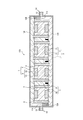
- FIG. 2 is a II-II sectional view showing a schematic structure of an example of the solar cell module shown in FIG.
- FIG. 3 is a III-III cross-sectional view showing a schematic structure of an example of the solar cell module shown in FIG. 1.
- FIG. 4 is a IV-IV sectional view for explaining a method for measuring the thickness of the sealing portion of the solar cell module shown in FIG. 1.
- the solar cell module of the present invention is not particularly limited, and may be a solar cell module such as a dye-sensitized solar cell, an organic thin film solar cell, and a perovskite solar cell.
- the solar cell module of the present invention can be a solar cell module in which a plurality of photoelectric conversion cells (hereinafter also simply referred to as “cells”) are connected in series, for example, a solar cell module having a Z-type integrated structure.
- the solar cell module integrated structure includes, for example, a series connection structure such as a W-type module and a monolithic module, or a parallel connection structure, but is not limited thereto.
- the dye-sensitized solar cell module having a Z-type integrated structure as an example of the present invention is not particularly limited.
- FIG. 1 is a plan view
- the solar cell module 100 which shows sectional drawing is mentioned.
- the solar cell module 100 shown in a plan view in FIG. 1 includes a barrier packaging material 13A and a barrier packaging material 13B (FIG. 1) that enclose a first substrate 3 that is a photoelectrode substrate and a second substrate 7 that is a counter electrode substrate.
- the first extraction electrode 11A connected to the first substrate 3 and the second extraction electrode 11B connected to the second substrate 7 are respectively extended from the solar cell module 100 to the outside of the module.
- the sealing part 14 to be taken out is provided.
- FIG. 2 shows a sectional view taken along the line II-II in FIG. 1
- FIG. 3 shows a sectional view taken along the line III-III in FIG.
- the solar cell module 100 is a dye-sensitized solar cell module in which a plurality of (four in the illustrated example) cells partitioned by the partition walls 8 are connected in series. It has an integrated structure.
- the solar cell module 100 includes a first base 1 and a first photoelectrode 2 that is a plurality of (four in the illustrated example) first electrodes provided on the first base 1 so as to be spaced apart from each other.
- the photoelectrode 2 and the counter electrode 6 forming each cell are opposed to each other via the electrolyte layer 4 which is a functional layer. (Ie, so as to form a cell), and between the adjacent cells, the photoelectrode 2 of one cell and the counter electrode 6 of the other cell are electrically connected via the cell connection portion 9. It has the structure bonded together.
- Each cell of the solar cell module 100 includes a photoelectrode 2, a counter electrode 6 facing the photoelectrode 2, and an electrolyte layer 4 provided between the photoelectrode 2 and the counter electrode 6.
- the solar cell module 100 includes a first extraction electrode 11A connected to the photoelectrode conductive layer 21 constituting the photoelectrode 2 via the first electrical connection portion 12A, and a counter electrode conductive constituting the counter electrode 6.
- a second extraction electrode 11B connected to the layer 61 via the second electrical connection portion 12B is provided.
- the barrier packaging materials 13 ⁇ / b> A and 13 ⁇ / b> B include a sealing portion 14 that extends the first extraction electrode 11 ⁇ / b> A from the solar cell module 100. Further, although not shown, the sealing portion 14 also extends the second extraction electrode 11 ⁇ / b> B from the solar cell module 100.
- the sealing part 14 is characterized by being sealed with a cured product of the cross-linking adhesive composition. Further, as is clear from FIG. 1, the sealing portion 14 surrounds the outer periphery of the solar cell module 100 and separates the solar cell module 100 from the external environment.
- the structure of the solar cell module of the present invention is not limited to the structure shown in FIGS.
- the first extraction electrode 11 ⁇ / b> A and the second extraction electrode 11 ⁇ / b> B extend from the same side of the sealing portion 14 formed on the outer periphery of the solar cell module 100.
- the solar cell module 100 may have a structure in which both the first extraction electrode 11A and the second extraction electrode 11B are extended from different sides of the sealing portion 14.
- the first and second extraction electrodes 11 ⁇ / b> A and 11 ⁇ / b> B are both disposed near the center in the thickness direction of the solar cell module 100.
- the first extraction electrode 11A is not particularly limited as long as the first extraction electrode 11A is electrically connected to the photoelectrode 2 and insulated from the counter electrode 6.
- the first extraction electrode 11A is closer to the second base material 5 than the first base material 1. You may arrange
- the second extraction electrode 11 ⁇ / b> B may be disposed at a position closer to the first base material 1 than the second base material 5.
- the first substrate 3 of the solar cell module 100 shown in FIGS. 1 to 3 includes a first base material 1 and a plurality of photoelectrodes 2 provided on the first base material 1 so as to be separated from each other.
- the photoelectrode 2 includes a photoelectrode conductive layer 21 provided on the first substrate 1 and a porous semiconductor fine particle layer 22 provided on a part of the photoelectrode conductive layer 21. .
- the photoelectrode conductive layer 21 is provided with a gap.
- the adjacent photoelectrodes 2 are provided so as to be electrically insulated from each other. This insulation is not particularly limited, and can be achieved, for example, by the partition walls 8 existing in the gaps between the photoelectrode conductive layers 21 adjacent to each other.
- the first substrate 1 is not particularly limited, and can be appropriately selected from known light-transmitting substrates.
- a 1st base material the known transparent base material which has transparency in visible regions, such as transparent resin and glass, is mentioned.
- the 1st base material 1 it is preferable to use the transparent resin shape
- the resin film substrate is inferior in the barrier property of the substrate itself as compared with a substrate such as glass, but the barrier property can be greatly improved by taking the structure of the present invention.
- the solar cell module can be provided with lightness and flexibility, and thus can be applied to various applications.
- transparent resins examples include polyethylene terephthalate (PET), polyethylene naphthalate (PEN), syndiotactic polystyrene (SPS), polyphenylene sulfide (PPS), polycarbonate (PC), and polyarylate (PAr).
- Synthetic resins such as polysulfone (PSF), polyester sulfone (PES), polyetherimide (PEI), transparent polyimide (PI), and cycloolefin polymer (COP).
- the photoelectrode conductive layer 21 is not particularly limited, and includes a conductive layer made of a metal mesh composed of Au, Ag, Cu, metal nanoparticles such as Ag nanoparticles, minute Ag wires, and the like. Includes conductive layers formed by coating, conductive layers made of complex metal oxides such as indium-tin oxide (ITO), indium-zinc oxide (IZO), and fluorine-doped tin (FTO), carbon nanotubes, graphene, etc. And a conductive layer made of a conductive polymer such as PEDOT / PSS (poly (3,4-ethylenedioxythiophene) polystyrene sulfonate). These materials can be appropriately selected depending on compatibility with other materials.
- PEDOT / PSS poly (3,4-ethylenedioxythiophene) polystyrene sulfonate
- a plurality of these conductive layers may be laminated on the base material, or various conductive materials as described above that can be used for forming these conductive layers are mixed to form one conductive layer. It may be formed.
- a known forming method such as a method in which sputtering and etching are combined or screen printing can be used.
- an undercoat layer (not shown) can be provided on the photoelectrode conductive layer 21.
- the electrolytic solution reaches the photoelectrode conductive layer 21 through the porous semiconductor fine particle layer 22, and passes from the photoelectrode conductive layer 21 to the electrolyte layer 4.
- An internal short circuit phenomenon called reverse electron transfer in which electrons leak can occur. For this reason, a reverse current unrelated to the light irradiation may occur and the photoelectric conversion efficiency may be reduced. Therefore, an undercoat layer can be provided on the photoelectrode conductive layer 21 to prevent such an internal short-circuit phenomenon.
- the adhesion between the porous semiconductor fine particle layer 22 and the photoelectrode conductive layer 21 can be improved by providing an undercoat layer on the photoelectrode conductive layer 21.
- the undercoat layer is not particularly limited as long as it is a substance that can prevent the internal short circuit phenomenon (interfacial reaction is unlikely to occur).
- it may be a layer containing a material such as titanium oxide, niobium oxide, or tungsten oxide.
- a method for forming the undercoat layer a method in which the above material is directly sputtered on the transparent conductive layer, a solution in which the above material is dissolved in a solvent, a solution in which a metal hydroxide that is a precursor of a metal oxide is dissolved, Alternatively, there is a method in which a solution containing a metal hydroxide obtained by dissolving an organometallic compound in a mixed solvent containing water is applied onto the conductive layer 21 for the photoelectrode, dried, and sintered as necessary.
- the porous semiconductor fine particle layer 22 carrying (adsorbing) a sensitizing dye is not particularly limited, and is a porous semiconductor fine particle layer containing particles of an oxide semiconductor such as titanium oxide, zinc oxide, tin oxide.
- a porous semiconductor fine particle layer formed by adsorbing a sensitizing dye such as an organic dye or a metal complex dye can be used.
- organic dyes include cyanine dyes, merocyanine dyes, oxonol dyes, xanthene dyes, squarylium dyes, polymethine dyes, coumarin dyes, riboflavin dyes, and perylene dyes.
- the metal complex dye examples include phthalocyanine complexes and porphyrin complexes of metals such as iron, copper, and ruthenium.
- Examples of typical sensitizing dyes include N3, N719, N749, D102, D131, D150, N205, HRS-1, and -2.
- the organic solvent for dissolving the sensitizing dye is preferably degassed and purified by distillation in advance in order to remove moisture and gas present in the solvent.
- Organic solvents include alcohols such as methanol, ethanol, propanol, nitriles such as acetonitrile, halogenated hydrocarbons, ethers, amides, esters, carbonates, ketones, hydrocarbons, aromatics, nitromethane, etc. Is preferred.
- a known forming method such as screen printing or coating can be used.
- a method for adsorbing the sensitizing dye to the porous semiconductor fine particle layer a known method such as immersion of the porous semiconductor fine particle layer in a solution containing the sensitizing dye can be used.
- the second substrate 7 of the solar cell module 100 includes a second base material 5 and a plurality of counter electrodes 6 provided on the second base material 5 so as to be separated from each other.
- the counter electrode 6 includes a counter electrode conductive layer 61 provided on the second substrate 5 and a catalyst layer 62 provided on a part of the counter electrode conductive layer 61.
- the catalyst layer 62 faces the porous semiconductor fine particle layer 22 of the photoelectrode 2.
- the counter electrodes 6 adjacent to each other are provided so as to be electrically insulated from each other. This insulation is not particularly limited, and can be achieved, for example, by interposing the partition wall 8 in the gap between the opposing electrodes 6 adjacent to each other.
- the 2nd base material 5 it is the same base material as the 1st base material 1, or the base material which does not have transparency like foil, plates, such as titanium, SUS, and aluminum, and other sun A base material free from corrosion by battery members can be used. Especially, it is preferable to form the 2nd base material 5 using a resin film for the same reason as the 1st base material 1.
- a conductive layer similar to the photoelectrode conductive layer 21 can be used as the counter electrode conductive layer 61.
- the catalyst layer 62 is not particularly limited, and includes any component that can function as a catalyst such as a conductive polymer, a carbon nanostructure, a noble metal particle, and a mixture of the carbon nanostructure and the noble metal particle.
- the catalyst layer can be used.
- the conductive polymer include poly (thiophene-2,5-diyl), poly (3-butylthiophene-2,5-diyl), and poly (3-hexylthiophene-2,5-diyl).
- Polythiophene such as poly (2,3-dihydrothieno- [3,4-b] -1,4-dioxin) (PEDOT); polyacetylene and derivatives thereof; polyaniline and derivatives thereof; polypyrrole and derivatives thereof; poly (p-xylene) Tetrahydrothiophenium chloride), poly [(2-methoxy-5- (2'-ethylhexyloxy))-1,4-phenylenevinylene], poly [(2-methoxy-5- (3 ', 7'- Dimethyloctyloxy) -1,4-phenylenevinylene)], poly [2-2 ′, 5′-bis (2 ′′ -ethylhexyloxy) phenyl] -1,4 Polyphenylene vinylenes such as -phenylene vinylene]; and the like.
- PEDOT poly (2,3-dihydrothieno- [3,4-b] -1,4-dioxin)
- PEDOT poly
- Examples of the carbon nanostructure include natural graphite, activated carbon, artificial graphite, graphene, carbon nanotube, and carbon nanobud.
- the noble metal particles are not particularly limited as long as they have a catalytic action, and known noble metal particles such as metal platinum, metal palladium, and metal ruthenium can be appropriately selected and used.
- the method for forming the catalyst layer is not particularly limited, and a known method can be appropriately selected and used.
- a conductive polymer, carbon nanostructures, noble metal particles, or a mixture obtained by dissolving or dispersing both carbon nanostructures and noble metal particles in an appropriate solvent is applied or sprayed onto the conductive film, It can be performed by drying the solvent of the mixed solution.
- a binder may be further added to the mixed solution.
- the binder from the viewpoint of dispersibility of the carbon nanostructure and adhesion to the substrate, a hydroxyl group, a carboxyl group, and a sulfonyl group. It is preferable to use a polymer having a functional group such as a group, a phosphate group, and a sodium salt of these functional groups.
- the catalyst layer is a carbon nanotube satisfying an average diameter (Av) of carbon nanotubes and a standard deviation ( ⁇ ) of diameter satisfying 0.60> 3 ⁇ / Av> 0.20 (hereinafter sometimes referred to as formula (A)).
- Av average diameter
- ⁇ standard deviation
- specific carbon nanotubes is a general term for a set of predetermined carbon nanotubes constituting the carbon nanotube, and “diameter” means an outer diameter of the predetermined carbon nanotube.
- the average diameter (Av) and standard deviation ( ⁇ ) of the diameter of a specific carbon nanotube are a sample average value and a sample standard deviation, respectively. They are determined as an average value and a standard deviation when measuring the diameter of 100 randomly selected carbon nanotubes under observation with a transmission electron microscope. 3 ⁇ in the formula (A) is obtained by multiplying the obtained standard deviation ( ⁇ ) by 3.
- a counter electrode having excellent catalytic activity can be obtained by using specific carbon nanotubes. From the viewpoint of improving the characteristics of the obtained counter electrode, 0.60> 3 ⁇ / Av> 0.25 is preferable, and 0.60> 3 ⁇ / Av> 0.50 is more preferable.
- 3 ⁇ / Av represents the diameter distribution of a specific carbon nanotube, and the larger this value, the wider the diameter distribution.
- the diameter distribution is preferably a normal distribution.
- the diameter distribution is measured by measuring the diameters of 100 randomly selected carbon nanotubes that can be observed using a transmission electron microscope, and using the results, the horizontal axis represents the diameter and the vertical axis represents the frequency. And plotting the resulting data and approximating with Gaussian.
- the value of 3 ⁇ / Av can also be increased by combining a plurality of types of carbon nanotubes obtained by different production methods, but in this case, it is difficult to obtain a normal distribution of diameters.
- the specific carbon nanotube may be a single carbon nanotube, or may be a single carbon nanotube mixed with another carbon nanotube in an amount that does not affect the diameter distribution.
- the specific carbon nanotube is a known method, for example, a substrate having a catalyst layer for producing carbon nanotubes (hereinafter sometimes referred to as “catalyst layer for producing CNT”) on the surface (hereinafter referred to as “substrate for producing CNT”).
- a catalyst layer for producing CNT hereinafter sometimes referred to as “catalyst layer for producing CNT”
- substrate for producing CNT a substrate having a catalyst layer for producing CNT
- CVD method chemical vapor deposition method
- a small amount of oxidant is present in the system, so that CNT It can be obtained by a method (supergrowth method) of dramatically improving the catalytic activity of the production catalyst layer (for example, International Publication No. 2006/011655).
- the carbon nanotube produced by the super growth method may be referred to as SGCNT.
- the counter electrode including a catalyst layer composed of specific carbon nanotubes for example, a dispersion containing specific carbon nanotubes is prepared, this dispersion is applied onto a substrate, and the resulting coating film is dried.
- the catalyst layer can be formed by forming the catalyst layer.
- the partition wall 8 of the solar cell module 100 is provided between the first substrate 3 and the second substrate 7 and surrounds each of the electrolyte layer 4 and the cell connection portion 9.
- the space in which the electrolyte layer 4 is provided and the space in which the cell connection portion 9 is provided are partitioned by the first substrate 3, the second substrate 7, and the partition walls 8.
- the partition wall 8 includes the photoelectrode conductive layer 21 of the photoelectrode 2 of the first substrate 3 and the second substrate 7 on one side in the width direction of each cell (left side in FIG. 2).
- the counter electrode conductive layer 61 of the counter electrode 6 (the portion located on the other side in the width direction than the portion where the catalyst layer 62 is formed) is provided.
- the electrolyte layers 4 and the cell connection portions 9 are alternately provided between the partition walls 8.
- the partition wall 8 is not particularly limited as long as it can adhere the first substrate 3 and the second substrate 7 and seal the electrolyte layer 4.
- the partition wall 8 is preferably excellent in adhesion between substrates, resistance to an electrolyte (chemical resistance), and high temperature and high humidity durability (moisture heat resistance).
- Examples of the partition wall material that can form such a partition wall 8 include a non-conductive thermoplastic resin, a thermosetting resin, and an active radiation (light, electron beam) curable resin.
- (meth) acryl means “acryl” or “methacryl”.
- a photocurable acrylic resin is preferable from the viewpoint of handleability.
- the partition wall 8 can be configured using a film formed by forming various resins as described above into a sheet shape.
- the electrolyte layer 4 that is a functional layer of the solar cell module 100 is provided in a space surrounded by the porous semiconductor fine particle layer 22 of the photoelectrode 2, the catalyst layer 62 of the counter electrode 6, and the partition walls 8.
- the electrolyte layer 4 is not particularly limited, and can be formed using any electrolytic solution, gel electrolyte, or solid electrolyte that can be used in the dye-sensitized solar cell.
- the cell connection part 9 of the solar cell module 100 electrically connects cells adjacent to each other in series.
- the cell connection portion 9 includes the photoelectrode conductive layer 21 of the photoelectrode 2 of the cell located on the right side in FIG. 2 and the counterelectrode conductive layer of the counter electrode 6 of the cell located on the left side in FIG. 61 is electrically connected.
- the cell connection portion 9 of the solar cell module 100 includes the wiring 91 formed on the photoelectrode conductive layer 21 of the photoelectrode 2 so as to be separated from the porous semiconductor fine particle layer 22, the first substrate 3, and the second substrate. 7 and the conductive resin composition 92 filled in the space surrounded by the partition walls 8.
- the cell connection part 9 is formed using the wiring 91 and the conductive resin composition 92.
- the cell connection part is a conductive resin. You may form using only a composition.
- the wiring may be formed on the counter electrode conductive layer 61 of the counter electrode 6.
- the wiring 91 is not particularly limited, and wiring made of a conductive material such as metal and metal oxide can be used. Among these, from the viewpoint of increasing the photoelectric conversion efficiency of the dye-sensitized solar cell module by reducing the resistance of the cell connection portion 9, the wiring 91 is a metal wiring such as a copper wiring, a gold wiring, a silver wiring, or an aluminum wiring. It is preferable to use it.
- a method for forming the wiring 91 on the photoelectrode conductive layer 21 a known forming method such as sputtering or screen printing can be used.
- the conductive resin composition 92 is not particularly limited, and it is preferable to use a composition containing a resin and conductive particles.
- the resin of the conductive resin composition 92 is not particularly limited, and is a (meth) acrylic resin; epoxy resins such as bisphenol type epoxy resin, novolac type epoxy resin, cyclic epoxy resin, and alicyclic epoxy resin; silicone Resin; and the like.
- Arbitrary hardening agents such as a radical initiator, a cationic hardening agent, and an anionic hardening agent, can be used for the said resin, and a polymerization form is not specifically limited, such as addition polymerization and ring-opening polymerization.
- the resin as the partition wall material and the resin of the conductive resin composition 92 may be the same or different.
- the conductive particles of the conductive resin composition 92 are not particularly limited, and include, for example, a metal such as Ag, Au, Cu, Al, In, Sn, Bi, and Pb, and an alloy including the metal. Particles and their oxides, conductive carbon particles, and the surface of organic compound particles such as resin particles and inorganic compound particles, conductive materials such as metals such as Ag, Au, Cu, and oxides of these metals, For example, particles coated with an Au / Ni alloy can be used. And it is preferable that the average particle diameter of electroconductive particle is 0.5 micrometer or more and 30 micrometers or less. Furthermore, it is preferable that the content rate of electroconductive particle is 0.1 volume% or more and 90 volume% or less.
- the cell connection part 9 using the conductive resin composition 92 described above is not particularly limited.
- the cell connection part 9 includes an uncured resin and conductive particles at a position where the cell connection part 9 is formed. It can be formed by filling a cured conductive resin composition and curing the filled uncured conductive resin composition.
- the first extraction electrode 11A and the second extraction electrode 11B connected to the photoelectrode 2 and the counter electrode 6 are not particularly limited, and a conductor formed of a general conductive material is used.
- a conductor formed of a general conductive material is used.
- Examples of such a conductor include a metal material selected from the group consisting of copper, aluminum, nickel, iron, and the like, and a conductor formed of an alloy material containing these metal materials.
- an electrode using copper as a conductor or a material using stainless steel as a base material is preferable. It is preferable that the conductor is as thin as possible because the step difference from the surroundings becomes smaller and the sealing performance is improved when sealed with a barrier packaging material.
- the thickness of the conductor is preferably 0.001 mm or more and 0.5 mm or less.
- the take-out electrode an electrode in which a part of the above-described conductor is coated with a conductive material that can be a material for forming the first and second electrical connection portions 12A and 12B can be used. Even in such a case, it is necessary that the take-out electrode is not coated with a conductor in the sealing portion 14 in order to ensure sealing in the sealing portion 14 described in detail later.
- the 2nd electrical connection part 12B which connects 11B is not specifically limited, It can form with a general electrical connection material.
- the first and second electrical connection portions 12A and 12B are formed of a conductive resin composition or solder.
- the “conductive resin composition” used for forming the first electrical connection portion 12A and the second electrical connection portion 12B is generally an adhesive or an adhesive as long as it has adhesiveness and conductivity. Includes materials that can be referred to as agents.
- adheresive means a material that can be bonded and integrated into an integrated state, and has fluidity before curing, but does not have adhesiveness before curing. Can be a material.
- adheresive means a material that can adhere objects to be bonded to each other by applying a little pressure at room temperature for a short time without using water, solvent, heat, etc. To do.
- a conductive resin composition the known composition containing conductive materials, such as a metal, a metal oxide, and a conductive carbon material, and arbitrary resin similarly to the conductive resin composition 92 mentioned above. Can be used.
- the first and second electrical connection portions using a conductive adhesive, and a conductive tape product in which a conductor and a conductive adhesive are integrated is also suitable.
- a conductive adhesive a conductive tape product in which a conductor and a conductive adhesive are integrated.
- solder the thing containing tin, silver, copper, bismuth, lead, a flux component, etc. can be used. It is preferable that the solder can be formed at a temperature that does not affect the element and the substrate.
- the conductors of the first extraction electrode 11A and / or the second extraction electrode 11B are in contact with the cured crosslinked adhesive composition 15 (hereinafter also simply referred to as “crosslinked adhesive 15”), and the sealing portion 14.
- the region where the film can be formed may be manufactured through a roughening treatment step or an oxidation treatment step. If the region in contact with the crosslinkable adhesive 15 on the conductor is roughened or has an oxide film, the adhesion with the crosslinkable adhesive composition becomes strong before curing, and the sealing portion 14 is sealed. Increases nature.
- each conductor of the first extraction electrode 11A and / or the second extraction electrode 11B has a surface roughness of at least a part of a region where the sealing portion 14 can be formed in contact with the cross-linking adhesive 15 is 0. It is preferably 0.005 ⁇ m or more and 0.5 ⁇ m or less. Furthermore, it is more preferable that the surface roughness is equal to or greater than the lower limit value over the entire region where each conductor can form the sealing portion 14 in contact with the cross-linking adhesive 15. If the surface roughness of each conductor is at least the above lower limit in at least a part of the region in contact with the cross-linking adhesive 15, the takeout electrode can be firmly held by the sealing portion 14, and the solar cell The retention rate of the module 100 can be further improved.
- the cross-linking adhesive 15 sufficiently penetrates into the irregularities on the surface of each conductor, and the takeout electrode can be firmly held by the sealing portion 14.
- the retention rate of the solar cell module 100 can be further improved.
- the first electrical connection portion 12 ⁇ / b> A and the second electrical connection portion 12 ⁇ / b> B are respectively connected to the photoelectrode 2 or the counter electrode 6 via a collector line formed in the same manner as the wiring 91. It may be connected.
- the sealing portion 14 is sealed with a cured crosslinked adhesive 15.
- the gap between the conductors of the first extraction electrode 11 ⁇ / b> A and the second extraction electrode 11 ⁇ / b> B and the barrier packaging materials 13 ⁇ / b> A and 13 ⁇ / b> B is cross-linked adhesive. Filled with a cured product of the composition.
- the gap between the barrier packaging materials 13 ⁇ / b> A and 13 ⁇ / b> B can be filled with a cured product of the cross-linking adhesive composition.
- the cured cross-linked adhesive 15 that forms the seal of the sealing portion 14 preferably has fluidity before curing. That is, the adhesive is preferably in a state of exhibiting fluidity such as liquid or gel before curing. Therefore, when the cross-linking adhesive is disposed on the sealing portion 14 and cured by a general method such as coating, the adhesion between the cured cross-linking adhesive 15 and the barrier packaging materials 13A and 13B is improved. Can be improved. Further, the first extraction electrode 11A and the second extraction electrode 11B shown in FIG. 2 have no coating and the conductor is exposed on the surface. As described above, even when each extraction electrode has a coating. Even so, it is necessary that the gap between the conductor and the barrier wrapping material is filled with the cured cross-linking adhesive 15 in the sealing portion 14. Thereby, the sealing property in the sealing part 14 can be improved and the retention rate of the solar cell module 100 can be improved.
- the cross-linking adhesive composition is not particularly limited, and examples thereof include a photocurable resin composition and a thermosetting resin composition. Especially, it is preferable to use a photocurable resin composition as a bridge
- the photocurable resin composition examples include an ultraviolet curable resin composition and a visible light curable resin composition, and it is preferable to use an ultraviolet curable resin composition.
- the ultraviolet curable resin composition include a (meth) acrylic resin composition, an epoxy resin composition, a fluorine resin composition, and an olefin resin composition. It is preferable to use a composition, an epoxy resin composition, or a fluorine resin composition. These may be used alone or in combination of two or more.
- a thermosetting resin composition the thermosetting resin composition which can be hardened at the temperature which does not vaporize the electrolyte which comprises the electrolyte layer 4 is mentioned. More specifically, thermosetting resin compositions having a curing temperature in the range of 60 ° C.
- thermosetting resin composition examples include, for example, a (meth) acrylic resin composition, an epoxy resin composition, a fluorine resin composition, a silicone resin composition, an olefin resin composition, and a polyisobutylene resin. Examples thereof include compositions. These may be used alone or in combination of two or more.
- the thickness of the sealing portion 14 is preferably 1 ⁇ m or more, preferably 250 ⁇ m or less, and more preferably 200 ⁇ m or less.
- the one where the thickness of the sealing part 14 is thinner is preferable. If the thickness of the sealing part 14 is thin, the cross-sectional area of the sealing is reduced, so that it is easy to prevent intrusion of water or the like from the outside. On the other hand, if the thickness of the sealing portion 14 is too thin, there is a possibility that no resin can intervene in the gap. Or when the thickness of the sealing part 14 becomes below the size of the constituent material of resin, etc. (an aggregate, a filler, etc.), there exists a possibility that stress may be applied to the barrier packaging materials 13A and 13B.
- the cross-linkable adhesive 15 forming the sealing portion 14 may be easily peeled off from the barrier packaging materials 13A and 13B. Therefore, it is preferable to select the thickness of the sealing portion 14 according to the material contained in the cross-linking adhesive 15. Specifically, when the thickness of the sealing portion 14 is equal to or greater than the lower limit, the sealing performance of the solar cell module 100 by the sealing portion 14 can be improved. And if the thickness of the sealing part 14 is below the said upper limit, the sealing cross-sectional area used as the penetration
- the barrier packaging materials 13A and 13B impart durability to the solar cell module 100 under high-temperature and high-humidity environmental conditions to which the solar cell module 100 can be exposed. Therefore, the barrier packaging material is preferably a packaging body having a barrier property against gas and water vapor. Further, in FIG. 2, two barrier packaging materials 13A and 13B are illustrated as barrier packaging materials. As apparent from FIG. 2, the barrier packaging material 13A is disposed on the first substrate 3 side, and the barrier packaging material 13B is disposed on the counter electrode side.
- the barrier packaging material is not limited to being two sheet-like packaging bodies respectively arranged in the thickness direction of the solar cell module as shown in FIG. 2.
- the barrier packaging material constitutes the solar cell module. You may be comprised with the cylindrical film open
- the inclusion mode of the first substrate 3 and the second substrate 7 by the barrier packaging materials 13A and 13B is not particularly limited, and the first substrate 3 / second substrate 7 and the barrier packaging material 13A / 13B are cross-linked.
- the adhesive composition may be in close contact with each other, and the first substrate 3 / second substrate 7 are included, but there is a space between these and the barrier packaging material 13A / 13B. It may be in a state filled with a filler or the like which is difficult to pass water vapor or gas. More specifically, although not shown, an adhesive layer may be interposed in at least a part of the gap between the first base material 1 / second base material 5 and the barrier packaging material 13A / 13B. By providing the adhesive layer, the sealing property of the solar cell module can be further improved.
- the adhesive layer when the adhesive layer is disposed on the first substrate 3 side that is the light incident side substrate, if there is an adhesive layer between the barrier packaging material 13A and the first substrate 3, the barrier packaging material 13A and the first substrate 3 No air layer is interposed between the first substrate 1 and the first substrate 3.
- the air layer has a refractive index greatly different from that of the barrier packaging material 13 ⁇ / b> A and the first base material 1. For this reason, the refractive index difference at the interface of the laminated structure of the barrier packaging material 13A-air layer-first substrate 1 becomes large. If the refractive index difference at the interface is large, the amount of light reflected at the interface increases, so that the utilization efficiency of incident light cannot be sufficiently improved.
- the difference in refractive index can be reduced and loss due to interface reflection can be reduced. Furthermore, if an adhesive layer is provided, the occurrence of interference fringes on the surface of the solar cell module can be suppressed by suppressing the reflection of light.
- a material having a refractive index value between the refractive index of the barrier packaging material 13A and the refractive index of the first base material 1 is selected as the material for forming the adhesive layer. Such a material can be selected from the materials listed as the partition material while taking into consideration the material of the barrier packaging material 13A and the material of the first base material 1, for example.
- the solar cell module is a dye-sensitized solar cell module
- the filler that hardly allows water vapor or gas to pass therethrough include liquid or gel paraffin, silicone, phosphate ester, and aliphatic ester.
- the barrier packaging materials 13A and 13B preferably have a water vapor permeability of 0.1 g / m 2 / day or less in an environment of a temperature of 40 ° C. and a relative humidity of 90% (90% RH), and 0.01 g / m 2 / day or less is more preferable, 0.0005 g / m 2 / day or less is further preferable, and 0.0001 g / m 2 / day or less is particularly preferable.
- the barrier packaging materials 13A and 13B preferably have a total light transmittance of 50% or more, more preferably 70% or more, and still more preferably 85% or more. Such total light transmittance can be measured, for example, according to JIS K7361-1.
- the barrier packaging materials 13A and 13B are preferably films in which a barrier layer having low water vapor and gas permeability is installed on a plastic support.
- barrier films with low gas permeability include those deposited with silicon oxide or aluminum oxide (Japanese Patent Publication No. 53-12953, Japanese Patent Laid-Open No. 58-217344), and those having an organic-inorganic hybrid coating layer (Japanese Patent Laid-Open No. 2000-2000).
- 323273, Japanese Unexamined Patent Application Publication No. 2004-25732 those having an inorganic layered compound (Japanese Unexamined Patent Application Publication No. 2001-205743), laminated inorganic materials (Japanese Unexamined Patent Application Publication No.
- the solar cell module 100 having the above-described configuration is not particularly limited, and can be manufactured by the following procedure, for example. Specifically, first, the first substrate 3 including the photoelectrode 2 is manufactured, and then the wiring 91 is formed on the manufactured first substrate 3. Next, an uncured conductive resin composition 92 is applied at a position overlapping the wiring 91, and a partition wall material is applied so as to surround the photoelectrode conductive layer 21 with the applied conductive resin composition 92 interposed therebetween. To do. Then, a component constituting the electrolyte layer 4 such as an electrolytic solution is filled in the region where the partition wall material is applied. Thereafter, the second substrate 7 including the counter electrode 6 is overlapped with the first substrate 3.
- the uncured conductive resin composition 92 is cured to form the cell connection portion 9 and the first substrate 3 and the second substrate 7 are firmly bonded to obtain a pair of electrode substrates.
- the first extraction electrode 11A and the second extraction electrode 11B are bonded to the photoelectrode 2 and the counter electrode 6 provided on the obtained pair of electrode substrates via a conductive adhesive, respectively (extraction electrode). Installation process).
- the cross-linking adhesive composition is applied to the barrier packaging materials 13A and 13B (application process), and the pair of electrode substrates to which the take-out electrodes are attached are sandwiched from above and below by the barrier packaging materials 13A and 13B. (Pinching process).
- the barrier packaging materials 13A and 13B and the conductor are brought into close contact with each other via the cross-linking adhesive composition (press adhesion).
- the solar cell module 100 having the above-described configuration in which the electrode substrate 3 and the second substrate 7 are packaged by the barrier packaging materials 13A and 13B is obtained.
- the extraction electrode attaching process to the pressing contact process will be described in detail.
- the first extraction electrode 11A is provided for the photoelectrode 2 provided on the pair of electrode substrates, and the second extraction electrode 11B is provided for the counter electrode 6 via a conductive resin composition or solder, respectively.
- the conductive resin composition or the solder is a material for forming the first and second electrical connection portions, but the conductive resin composition or the solder is arranged in advance with respect to the conductor of the extraction electrode. Preferably it is.
- the first extraction electrode and the second extraction electrode can be formed by using a conductive resin composition or solder as described above that is pre-coated on the conductor of the extraction electrode.
- the conductor is attached to the photoelectrode 2 or the counter electrode 6 so that the conductive resin composition or the solder on at least a part of the conductor exhibits adhesiveness by a known method such as heating.
- a known method such as heating.
- the manufacturing efficiency of the solar cell module 100 can be improved.
- the extraction electrode is formed using a conductor pre-coated with a conductive resin composition or solder, it is a region other than the portion to be attached to the photoelectrode 2 / counter electrode 6 and is at least sealed. It is preferable that such a coating is removed in advance in a region in contact with the stopper 14. This is because the sealing performance of the sealing portion can be improved.
- the cross-linking adhesive composition is applied onto the barrier packaging materials 13A and 13B by a general coating means that can be used for coating a fluid object such as a dispenser method or a screen printing method. Apply to. And the application quantity of a bridge
- the cross-linking adhesive composition preferably has a viscosity of 10 Pa ⁇ s or more, more preferably 40 Pa ⁇ s or more, preferably 200 Pa ⁇ s or less, and 160 Pa ⁇ s or less. More preferably, it is more preferably 100 Pa ⁇ s or less. If the viscosity is equal to or higher than the above lower limit value, it is possible to easily form a sealing portion having a desired thickness, improve the sealing property of the sealing portion, and obtain good coating properties. it can. Moreover, if a viscosity is below the said upper limit, it can suppress that the thickness of a sealing part becomes thick too much, and can improve the sealing performance of a sealing part.
- the barrier wrapping material is arranged with the exposed surface of the electrode substrate 3 and the second substrate 7 bonded to each other facing the surface where the cross-linking adhesive composition is applied in the application step.
- the two barrier packaging materials 13A and 13B may be arranged on the exposed surface of the electrode substrate 3 and the exposed surface of the second substrate 7, respectively, or one barrier packaging material may be folded to The exposed surface of the first substrate 3 and the exposed surface of the second substrate 7 may be sandwiched from above and below.
- the cross-linking adhesive composition is used while pressing the pair of substrates constituted by the first substrate 3 or the second substrate 7 and the barrier packaging material 13 in the thickness direction of the solar cell module 100 by the pressing member.
- the conductor of the take-out electrode and the barrier wrapping material are brought into close contact with each other through the cross-linking adhesive composition.
- the pressing member it is possible to use a member having a recess that fits into the pair of substrates described above at least in a pressed state. More specifically, as the pressing member, an elastic body that can generate a recess that fits into the pair of substrates in a pressed state when pressed against the pair of substrates in this step can be used.
- an elastic body in addition to the effect of forming a recess, it is possible to apply pressure in a state of close contact with the surrounding area, such as around the extraction electrode, in close contact with the level difference. An increase in the sealing cross-sectional area can be suppressed.
- Such an elastic body is not particularly limited, and examples thereof include natural rubber, diene rubber, non-diene rubber, and thermoplastic elastomer. Among these, silicone rubber which is non-diene rubber is preferable.
- the elastic body needs to have a hardness that can deform the barrier packaging material at least in the pressed state in the region on the barrier packaging material adjacent to the pair of substrates. For this reason, the hardness of the elastic body is appropriately selected depending on the material of the barrier packaging material used.
- the pressing member it is possible to use a pressing member in which the hardness of the elastic body in the portion in contact with the region on the barrier packaging material adjacent to the pair of substrates is higher than the hardness of the elastic body in the portion in contact with the pair of substrates.
- the pressing member it is possible to use a member that is formed of an elastic body as described above and that has a concave portion that fits in advance with a pair of substrates, that is, a member that has the concave portion in a non-pressed state. By using this pressing member in this step, it is possible to efficiently press the region on the barrier packaging material adjacent to the pair of substrates, and to efficiently form the sealing portion 14 with high hermeticity.
- ⁇ Viscosity of crosslinkable adhesive composition The viscosity of the crosslinked adhesive compositions used in Examples and Comparative Examples was measured at 25 ° C. using a cone plate viscometer (cone angle 3 °, rotation speed 2.5 rpm).
- ⁇ Thickness of sealing part> The sealing part of the solar cell module produced by the Example and the comparative example cut
- the cutting position is such that the obtained cut surface exposes the cross section of the copper foil constituting the extraction electrode, the layer made of the cured cross-linked adhesive forming the sealing portion, and the barrier film as the barrier packaging material The position.
- Such a cutting position can be, for example, a cutting position along line IV-IV in FIG.
- FIG. 4 sectional drawing for demonstrating the measuring method of the thickness of the sealing part of a solar cell module is shown.
- the sealing part 14 in the sealing part 14, the gaps between the first extraction electrode 11A or the second extraction electrode 11B and the barrier packaging materials 13A and 13B, and the gaps between the barrier packaging materials 13A and 13B It is filled with a cross-linked adhesive 15 in a cured state.
- the first extraction electrode 11A and the second extraction electrode 11B are not coated with a conductor at least in the sealing portion 14, and the outer surfaces of the conductors have the first extraction electrode 11A and the second extraction electrode 11B according to the drawing. Match the outer surface of the.
- the thickness of the sealing part 14 is the thickness T 1 ( ⁇ m) of the gap between the barrier packaging materials 13A and 13B as shown in FIG. 4 and the first extraction electrode 11A (or the second extraction electrode 11B).
- a value obtained by subtracting the thickness T A2 ( ⁇ m) of the first extraction electrode 11A (or the second extraction electrode 11B) from the thickness T A1 ( ⁇ m) of the gap between the barrier wrapping materials 13A and 13B in the enclosed region is 2 in calculating the average value of the value T a obtained by dividing.
- These thicknesses T 1 , T A1 , and T A2 can be measured by observing the cut surface with a scanning electron microscope (SEM).
- T 1 and T A were measured at four different positions, respectively, and the average value was calculated as the thickness of the sealing portion 14.
- ⁇ Retention rate of solar cell module> The solar cell modules produced in Examples and Comparative Examples were connected to a source meter (2400 type source meter, manufactured by Keithley).
- a source meter 2400 type source meter, manufactured by Keithley.
- a pseudo solar light source PEC-L11 type, manufactured by Pexel Technologies Co., Ltd.
- an AM1.5G filter was attached to a 150 W xenon lamp light source device was used.
- the light amount of the light source was adjusted to 1 sun (about 100,000 lux AM1.5G, 100 mWcm ⁇ 2 (JIS C8912 class A)) and irradiated to the solar cell module.
- the output voltage was measured while changing the bias voltage from 0 V to 0.8 V in units of 0.01 V under 1 sun light irradiation, and current-voltage characteristics were obtained. Similarly, measurement was performed by stepping the bias voltage from 0.8 V to 0 V in the reverse direction, and the average value of the measurements in the forward direction and the reverse direction was used as photocurrent data. The initial photoelectric conversion efficiency (%) was calculated from the current-voltage characteristics and photocurrent data thus obtained. Next, after the dye-sensitized solar cell module was held in an environment of 65 ° C. and 90% RH for 300 hours, the current-voltage characteristics were measured in the same manner as described above.
- Example 1 ⁇ Preparation of dye solution> 72 mg of ruthenium complex dye (N719, Solaronics) was placed in a 200 mL volumetric flask. 190 mL of dehydrated ethanol was mixed and stirred. After stoppering the volumetric flask, the mixture was stirred for 60 minutes by vibration with an ultrasonic cleaner. After keeping the solution at room temperature, dehydrated ethanol was added to make a total volume of 200 mL to prepare a dye solution.
- ruthenium complex dye N719, Solaronics
- a transparent conductive substrate obtained by coating a transparent substrate (polyethylene naphthalate film, thickness 200 ⁇ m) as a first base material with a transparent conductive layer (indium tin oxide (ITO)) as a conductive layer for a photoelectrode. 13 ohm / sq.) Is printed and coated with conductive silver paste (K3105, manufactured by Pernox Co., Ltd.) as a wiring (collecting current) by screen printing at intervals according to the width of the photoelectrode cell. Wiring was produced by heating and drying in a circulation oven for 15 minutes.
- ITO indium tin oxide
- the obtained transparent conductive substrate having wiring was set on a coating coater with the wiring formation surface facing up, and an organic PC-600 solution (manufactured by Matsumoto Fine Chemical) diluted to 1.6% was swept with a wire bar ( 10 mm / sec).
- the obtained coating film was dried at room temperature for 10 minutes, and then further heated and dried at 150 ° C. for 10 minutes to produce an undercoat layer on the transparent conductive substrate.
- Laser treatment was performed on the undercoat layer forming surface of the transparent conductive substrate at intervals corresponding to the photoelectrode cell width to form insulating wires.
- a porous semiconductor fine particle layer is applied to a mask film (bottom: PC-542PA manufactured by Fujimori Kogyo Co., Ltd., NBO-0424 manufactured by Fujimori Kogyo Co., Ltd.) obtained by stacking two layers of protective films coated with an adhesive layer on a polyester film. An opening (length: 60 mm, width 5 mm) for forming was punched. The processed mask film was bonded to the current collector forming surface of the transparent conductive substrate on which the undercoat layer was formed so that air bubbles would not enter.
- the first layer of the mask film is for the purpose of preventing the dye from adhering to unnecessary portions
- the second layer is for the purpose of preventing the porous semiconductor fine particles from adhering to the unnecessary portions.
- a transparent conductive substrate sheet resistance obtained by coating a transparent substrate (polyethylene naphthalate film, thickness 200 ⁇ m) as a second base material with a transparent conductive layer (indium tin oxide (ITO)) as a conductive layer for a counter electrode.
- the conductive resin composition is linearly formed at a position overlapping the wiring between the photoelectrode cells when facing the first substrate between the catalyst layers, and a liquid material which is a partition material is formed on the outer peripheral portion of the catalyst layer with the line interposed therebetween.
- An ultraviolet curable sealant TB3035B manufactured by Three Bond Co., Ltd., absorption wavelength: 200 nm to 420 nm, viscosity: 51 Pa ⁇ s
- a dispenser device was applied by a dispenser device.
- a predetermined amount of the electrolyte solution is applied to the catalyst layer portion, and is superposed in a reduced pressure environment so that the rectangular catalyst layer and the porous semiconductor fine particle layer of the same type face each other using an automatic laminating apparatus.
- connection bodies including a plurality of cells is cut out from the bonded substrates, and the conductive copper foil tape is formed on the wirings arranged at both ends (extraction electrode portions) of the connection body.
- CRC7636D manufactured by Sony Chemical & Information Device Co., Ltd., copper foil thickness as a conductor: 35 ⁇ m
- the surface of the conductive copper foil tape used in this example is previously coated with a conductive adhesive made of a conductive acrylic resin.
- the electrical connection portion interposed between the photoelectrode / counter electrode and the extraction electrode is formed by a conductive adhesive coated on the conductor forming the extraction electrode.
- the conductive copper foil tape for forming the extraction electrode prior to attachment, the conductive portion of the portion other than the region used for attachment to the photoelectrode / counter electrode (that is, the region for forming the electrical connection portion) is used. What removed the coating of the adhesive was used. The removed portion had a surface roughness Ra of 0.035 ⁇ m. The surface of the copper foil tape where the conductive coating was removed was exposed to air and naturally oxidized to have an oxide film.
- barrier films Nao Seeds, “Ultra High Barrier Film”, water vapor permeability: 0.00005 g / m 2 / day
- a barrier packaging material that is larger than the connected body of a plurality of cut cells
- Cross-linking for forming a sealing part on the entire surface of the connection body, on the barrier film including the surface of the conductive copper foil tape (coating removed) on the outer periphery, and on the back surface of the conductive copper foil tape on the outer periphery
- a liquid UV-curable crosslinking adhesive composition manufactured by ThreeBond Co., Ltd., “TB3035B”, acrylic resin, which is a mold adhesive composition, was applied.
- the viscosity of the ultraviolet curable cross-linking adhesive composition was measured according to the above method, it was 51 Pa ⁇ s at 25 ° C.
- a pair of upper and lower pressing members which are jigs having protruding surfaces made of rubber materials protruding from the portions near the outer peripheral portions of the first substrate and the second substrate, are sandwiched between the lower members by a barrier film.
- the connected body was placed.
- another barrier film is stacked from above, a portion that contacts the vicinity of the outer peripheral portion of the substrate from the top is made of a silicone rubber material, and a portion that contacts the substrate is a sponge silicone rubber material whose hardness is lower than that of the material.
- pressure was applied in the thickness direction, light irradiation was performed from both sides, and a connection body of a plurality of cells was covered with a barrier film.
- Example 2 Conductive paste doughite is used as the conductive resin composition for forming the electrical connection portion by forming the extraction electrode using a copper foil having a thickness of 35 ⁇ m and a surface roughness Ra of 0.3 ⁇ m instead of the conductive copper foil tape.
- Regular trademark manufactured by Fujikura Kasei Co., Ltd., “Dotite D-362”
- Various measurements and evaluations were performed. The results are shown in Table 1.
- Example 3 As a crosslinkable adhesive composition for forming a sealing portion, the viscosity at 25 ° C. measured in accordance with the above method was used instead of a liquid ultraviolet curable crosslinkable adhesive composition (manufactured by ThreeBond, “TB3035B”). A dye-sensitized solar cell in the same manner as in Example 1, except that a liquid UV-curable crosslinking adhesive composition (manufactured by ThreeBond, “TB3118”, absorption wavelength: 200 nm to 350 nm) of 86 Pa ⁇ s was used. A module was prepared, and various measurements and evaluations were performed. The results are shown in Table 1.
- Example 4 As a crosslinkable adhesive composition for forming a sealing portion, the viscosity at 25 ° C. measured in accordance with the above method was used instead of a liquid ultraviolet curable crosslinkable adhesive composition (manufactured by ThreeBond, “TB3035B”). Dye sensitization in the same manner as in Example 1 except that a liquid UV-curable cross-linking adhesive composition (manufactured by Nichiban Co., Ltd., “Nichiban UM”, absorption wavelength: 200 nm to 420 nm) at 150 Pa ⁇ s was used. A solar cell module was prepared and subjected to various measurements and evaluations. The results are shown in Table 1.
- Example 1 A dye-sensitized solar cell module was prepared in the same manner as in Example 1 except that a conductive copper foil tape in a state where the conductive adhesive coating was not removed was used as the extraction electrode, and various measurements and evaluations were performed. . The results are shown in Table 1.
- a solar cell module that has a barrier packaging material that protects the solar cell module from the external environment and that has an excellent photoelectric conversion efficiency retention rate.
Landscapes
- Engineering & Computer Science (AREA)
- Power Engineering (AREA)
- Microelectronics & Electronic Packaging (AREA)
- Chemical & Material Sciences (AREA)
- Chemical Kinetics & Catalysis (AREA)
- Electrochemistry (AREA)
- Materials Engineering (AREA)
- Hybrid Cells (AREA)
- Photovoltaic Devices (AREA)
- Life Sciences & Earth Sciences (AREA)
- Sustainable Development (AREA)
- Sustainable Energy (AREA)
Abstract
Description
そこで、本発明は、太陽電池モジュールを外部環境から保護するバリア包装材を有する、光電変換効率の保持率に優れる、太陽電池モジュールを提供することを目的とする。
なお、本明細書において「非導電性」とは太陽電池特性に悪影響を与えるリーク電流を流さない体積抵抗を有することを意味し、例えば体積抵抗が107Ω・cm以上であることをいう。
なお、本明細書において「導電性」とは少なくとも接続方向における電気的接続が可能であることを意味し、太陽電池特性の観点から電気抵抗が低いほど好ましい。導電性樹脂、或いは後述する導電性樹脂組成物は、例えば、当該導電性樹脂を用いて、又は導電性樹脂組成物を硬化して太陽電池モジュールを形成した場合に、導電性樹脂又は硬化状態の導電性樹脂組成物の接続方向における抵抗が太陽電池モジュールの特性低下に大きな影響を及ぼさなければよい。具体的には、導電性樹脂又は硬化状態の導電性樹脂組成物の単位面積抵抗が0.5Ω・cm2以下であることが好ましい。なお、単位面積抵抗は、接続方向における両端を抵抗率計で測定した値と、接続方向に垂直な方向における断面積から求めることができる。
なお、本明細書において封止部の「厚み」は、太陽電池モジュールの厚さ方向における、封止断面上でのバリア包装材間の最短距離、及びバリア包装材と取出し電極との間の最短距離を求め、これらの平均値を算出して得られる値である。
かかる製造方法によれば、本発明の太陽電池モジュールを良好に製造することができる。
ここで、図1に平面図を示す太陽電池モジュール100は、光電極基板である第1基板3及び対向電極基板である第2基板7を内包するバリア包装材13A及びバリア包装材13B(図1には図示しない)を備え、第1基板3に接続された第1取り出し電極11Aと、第2基板7に接続された第2取り出し電極11Bとを、それぞれ太陽電池モジュール100からモジュール外部へと延出させる封止部14を備える。
ここで、図1~3に示す太陽電池モジュール100の第1基板3は、第1基材1と、第1基材1上に互いに離隔させて設けられた複数の光電極2とを備えている。また、光電極2は、第1基材1上に設けられた光電極用導電層21と、光電極用導電層21上の一部に設けられた多孔質半導体微粒子層22とを備えている。なお、光電極用導電層21は、隙間をあけて設けられている。そして、互いに隣接する光電極2同士は、互いに電気的に絶縁されるように設けられている。この絶縁は、特に限定されることなく、例えば互いに隣接する光電極用導電層21間の隙間に存在する隔壁8によって達成することができる。
なお、第1基材1上に光電極用導電層21を形成する方法としては、スパッタリングとエッチングとを組み合わせた方法や、スクリーン印刷など、既知の形成方法を用いることができる。
下塗り層は、内部短絡現象を防ぐことのできる(界面反応が起こりにくい)物質であれば、特に限定はされない。例えば、酸化チタン、酸化ニオブ、酸化タングステン等の材料を含んでなる層でありうる。また、下塗り層を形成する方法としては、上記材料を透明導電層に直接スパッタする方法、あるいは上記材料を溶媒に溶解した溶液、金属酸化物の前駆体である金属水酸化物を溶解した溶液、又は有機金属化合物を水を含む混合溶媒に溶解して得た金属水酸化物を含む溶液を、光電極用導電層21上に塗布、乾燥し、必要に応じて焼結する方法がある。
また、太陽電池モジュール100の第2基板7は、第2基材5と、第2基材5上に互いに離隔させて設けられた複数の対向電極6とを備えている。また、対向電極6は、第2基材5上に設けられた対向電極用導電層61と、対向電極用導電層61上の一部に設けられた触媒層62とを備えている。そして、触媒層62は、光電極2の多孔質半導体微粒子層22に対向している。
なお、互いに隣接する対向電極6同士は、互いに電気的に絶縁されるように設けられている。この絶縁は、特に限定されることなく、例えば互いに隣接する対向電極6間の隙間に隔壁8を介在させることにより、達成することができる。
ここで、導電性高分子としては、例えば、ポリ(チオフェン-2,5-ジイル)、ポリ(3-ブチルチオフェン-2,5-ジイル)、ポリ(3-ヘキシルチオフェン-2,5-ジイル)、ポリ(2,3-ジヒドロチエノ-[3,4-b]-1,4-ジオキシン)(PEDOT)等のポリチオフェン;ポリアセチレンおよびその誘導体;ポリアニリンおよびその誘導体;ポリピロールおよびその誘導体;ポリ(p-キシレンテトラヒドロチオフェニウムクロライド)、ポリ[(2-メトキシ-5-(2’-エチルヘキシロキシ))-1,4-フェニレンビニレン]、ポリ[(2-メトキシ-5-(3’,7’-ジメチルオクチロキシ)-1,4-フェニレンビニレン)]、ポリ[2-2’,5’-ビス(2’’-エチルヘキシロキシ)フェニル]-1,4-フェニレンビニレン]等のポリフェニレンビニレン類;などを挙げることができる。
炭素ナノ構造体としては、例えば、天然黒鉛、活性炭、人造黒鉛、グラフェン、カーボンナノチューブ、カーボンナノバッドなどを挙げることができる。
貴金属粒子としては、触媒作用のあるものであれば特に限定されず、金属白金、金属パラジウム、及び金属ルテニウムなどの公知の貴金属粒子を適宜選択して用いることができる。
なお、製造容易性の観点から、上述したような各種樹脂がシート状に成形されてなるフィルムを用いて、隔壁8を構成することももちろん可能である。
また、太陽電池モジュール100の機能層である電解質層4は、光電極2の多孔質半導体微粒子層22と、対向電極6の触媒層62と、隔壁8とで囲まれる空間に設けられている。そして、電解質層4は、特に限定されることなく、色素増感型太陽電池において使用し得る任意の電解液、ゲル状電解質又は固体電解質を用いて形成することができる。
そして、太陽電池モジュール100のセル接続部9は、光電極2の光電極用導電層21上に多孔質半導体微粒子層22と離隔させて形成された配線91と、第1基板3、第2基板7および隔壁8で囲まれた空間内に充填された導電性樹脂組成物92とで構成されている。なお、図2に示す太陽電池モジュール100では配線91と導電性樹脂組成物92とを用いてセル接続部9を形成しているが、本発明の太陽電池モジュールでは、セル接続部は導電性樹脂組成物のみを用いて形成してもよい。また、配線は、対向電極6の対向電極用導電層61上に形成してもよい。
そして、導電性粒子の平均粒子径は、0.5μm以上30μm以下であることが好ましい。更に、導電性粒子の含有割合は、0.1体積%以上90体積%以下であることが好ましい。
そして、光電極2と対向電極6に対して、それぞれ接続された、第1取り出し電極11A及び第2取り出し電極11Bは、特に限定されることなく、一般的な導電性材料により形成された導体を有する。そのような導体としては、銅、アルミニウム、ニッケル、及び鉄等からなる群から選ばれる金属材料、及びこれらの金属材料を含む合金材料により形成された導体が挙げられる。中でも、銅を導体とする電極或いは、ステンレスを基材とするものが好ましい。
導体はなるべく厚みが薄い方が、バリア包装材で封止したとき周囲との段差が小さくなり封止性が高まるため好ましい。更には取出し電極として使用に問題ない強度を保つことが好ましい。具体的には、導体の厚みは、0.001mm以上0.5mm以下であることが好ましい。
なお、取り出し電極として、任意で、上述した導体の一部が第1及び第2の電気的接続部12A及び12Bの形成材料となりうる導電性材料によりコーティングされたものを用いることができる。そのような場合であっても、取り出し電極は、後に詳述する封止部14における密閉性を確保するために、封止部14においては、導体がコーティングされていないことが必要である。
そして、導電性樹脂組成物としては、上述した導電性樹脂組成物92と同様に、金属、金属酸化物、導電性炭素材料などの導電性を有する材料と、任意の樹脂とを含む既知の組成物を用いることができる。中でも、製造効率向上の観点から、導電性粘着剤を用いて第1及び第2電気的接続部を形成することが好ましく、導体と導電性粘着剤が一体となった導電性テープ製品等も好適に使用できる。
はんだとしては、錫、銀、銅、ビスマス、鉛、フラックス成分などを含有したものを使用することができる。はんだは素子や基材に影響を与えない温度で形成可能なものであることが好ましい。
さらに、封止部14は、硬化状態の架橋型接着剤15により封止されている。具体的には、図3に示すように、封止部14では、第1取り出し電極11A及び第2取り出し電極11Bの導体と、バリア包装材13A及び13Bとの間の間隙が、架橋型接着剤組成物の硬化物で充填されている。さらに、図2に示すように、封止部14では、バリア包装材13A及び13Bの間の間隙が、架橋型接着剤組成物の硬化物で充填されうる。ここで、封止部14の封止を形成する硬化状態の架橋型接着剤15は、硬化前には流動性を有することが好ましい。すなわち、接着剤は、硬化前には、液状又はゲル状のような、流動性を呈する状態であることが好ましい。したがって、塗布等の一般的な方法により架橋型接着剤を封止部14に配置して硬化した際に、硬化状態の架橋型接着剤15とバリア包装材13A及び13Bとの間の密着性を向上させることができる。
さらに、図2に示す第1取り出し電極11A及び第2取り出し電極11Bはコーティングを有さず、導体が表面に露出した状態であるが、上述したように、たとえ、各取り出し電極がコーティングを有する場合であっても、封止部14内では、導体とバリア包装材との間の間隙が硬化された架橋型接着剤15により充填されていることが必要である。これにより、封止部14における、密閉性を向上させて、太陽電池モジュール100の保持率を向上させることができるからである。
光硬化性樹脂組成物としては、紫外線硬化型樹脂組成物、及び可視光硬化型樹脂組成物が挙げられるが、紫外線硬化型樹脂組成物を用いることが好ましい。紫外線硬化型樹脂組成物の具体例としては、(メタ)アクリル系樹脂組成物、エポキシ系樹脂組成物、フッ素系樹脂組成物、オレフィン系樹脂組成物等が挙げられるが、なかでも、アクリル系樹脂組成物、エポキシ系樹脂組成物、又はフッ素系樹脂組成物を用いることが好ましい。これらは1種類のみを単独で、或いは2種類以上を混合して用いてもよい。
熱硬化性樹脂組成物としては、電解質層4を構成する電解質を気化させない温度で硬化可能な熱硬化性樹脂組成物が挙げられる。より具体的には、硬化温度が60℃~200℃の範囲内、なかでも80℃~180℃の範囲内、さらには100℃~160℃の範囲内である熱硬化性樹脂組成物が挙げられる。熱硬化性樹脂組成物の具体例としては、例えば、(メタ)アクリル系樹脂組成物、エポキシ系樹脂組成物、フッ素系樹脂組成物、シリコーン系樹脂組成物、オレフィン系樹脂組成物、ポリイソブチレン樹脂組成物等が挙げられる。これらは1種類のみを単独で、或いは2種類以上を混合して用いてもよい。
そして、バリア包装材13A及び13Bは、太陽電池モジュール100が曝されうる高温且つ高湿度の環境条件下で、太陽電池モジュール100に対して耐久性を付与する。従って、バリア包装材は、ガスや水蒸気に対するバリア性のある包装体であることが好ましい。さらに、図2では、バリア包装材として、2枚のバリア包装材13A及び13Bを図示する。図2から明らかなように、バリア包装材13Aは第1基板3側に配置されており、バリア包装材13Bは対向電極側に配置されている。しかし、バリア包装材は図2に示したような太陽電池モジュールの厚み方向上下にそれぞれ配置された2枚のシート状の包装体であることには限定されず、例えば、太陽電池モジュールを構成する複数のセルの奥行き方向(図1では左右方向)で開放している筒状のフィルムにより構成されていても良い。
また、特に、太陽電池モジュールが色素増感型太陽電池モジュールの場合には、用いる色素の吸収波長域における光の透過率が高い材料を接着層の形成材料として選択することが好ましい。
なお、水蒸気やガスを通しにくい充填材としては、例えば、液状又はゲル状のパラフィン、シリコーン、リン酸エステル、脂肪族エステルなどが挙げられる。
さらに、バリア包装材13A及び13Bは、全光線透過率が好ましくは50%以上、より好ましくは70%以上、更に好ましくは85%以上である。このような全光線透過率は、例えばJIS K7361-1により測定することができる。
上述した構成を有する太陽電池モジュール100は、特に限定されることなく、例えば、以下のような手順により製造することができる。具体的にはまず、光電極2を備える第1基板3を作製した後、作製した第1基板3の上に、配線91を形成する。次に、配線91に重なる位置に、未硬化の導電性樹脂組成物92を塗布し、さらに塗布した導電性樹脂組成物92を挟んでそれぞれ光電極用導電層21を囲むように隔壁材料を塗布する。そして、隔壁材料を塗布した領域内に電解液などの電解質層4を構成する成分を充填する。その後、対向電極6を備える第2基板7を、第1基板3と重ね合わせる。さらに、未硬化の導電性樹脂組成物92を硬化させてセル接続部9を形成すると共に第1基板3と第2基板7とを強固に接着させて、一対の電極基板を得る。
得られた一対の電極基板に備えられる光電極2及び対向電極6に対して、導電性接着剤を介して、それぞれ、第1取り出し電極11Aと、第2取り出し電極11Bとを接着させる(取り出し電極取り付け工程)。そして、バリア包装材13A及び13Bに対して、架橋型接着剤組成物を塗布し(塗布工程)、かかるバリア包装材13A及び13Bにより取り出し電極を取り付けた上記一対の電極基板を上下面から挟みこむ(挟み込み工程)。さらに、押圧部材によりバリア包装材13A及び13Bを介して一対の基板を厚み方向に押圧しつつ、バリア包装材13A及び13B及び導体を、架橋型接着剤組成物を介して密着させて(押圧密着工程)、電極基板3及び第2基板7がバリア包装材13A及び13Bにより包装されてなる上述した構成を有する太陽電池モジュール100を得る。以下、取り出し電極取り付け工程~押圧密着工程について詳述する。
取り出し電極取り付け工程では、一対の電極基板に備えられる光電極2に対して第1取り出し電極11Aを、対向電極6に対して第2取り出し電極11Bを、それぞれ、導電性樹脂組成物又ははんだを介して取り付ける。ここで、導電性樹脂組成物又ははんだは第1及び第2の電気的接続部の形成材料であるが、かかる導電性樹脂組成物又ははんだは、取り出し電極の導体に対して、予め配置されていることが好ましい。具体的には、上述したような導電性樹脂組成物又ははんだが、取り出し電極の導体に対して予めコーティングされたものを用いて、第1取り出し電極及び第2取り出し電極を形成することができる。この場合、加熱等の既知の方法により、導体の少なくとも一部上の導電性樹脂組成物又ははんだが接着性を発揮する状態として、導体を光電極2又は対向電極6に対してそれぞれ取り付ける。このように、電気的接続部の形成材料が予め部分的に配置された導体によれば、太陽電池モジュール100の製造効率を向上させることができる。
さらに、導電性樹脂組成物又ははんだにより予めコーティングされている導体を用いて取り出し電極を形成する場合には、光電極2/対向電極6に対して取り付ける部分以外の領域であって、少なくとも、封止部14と接する領域において、かかるコーティングを予め除去しておくことが好ましい。これにより、封止部の密閉性を向上することができるからである。
塗布工程では、ディスペンサー法や、スクリーン印刷法のような、流動性を有する対象物を塗布するために用いられうる一般的な塗布手段により、架橋型接着剤組成物をバリア包装材13A及び13B上に塗布する。そして、架橋型接着剤組成物の塗布量は、封止部14の密閉性、バリア包装材13Aと第1基板3との密閉性、並びにバリア包装材13Bと第2基板7との密着性を良好とすることができるように適宜決定することができる。さらには、少なくとも封止部14の厚みが上述した好適範囲内となるような塗布量とすることが好ましい。
ここで、架橋型接着剤組成物は、粘度が10Pa・s以上であることが好ましく、40Pa・s以上であることがより好ましく、200Pa・s以下であることが好ましく、160Pa・s以下であることがより好ましく、100Pa・s以下であることが更に好ましい。粘度が上記下限値以上であれば、所望の厚さの封止部を容易に形成することができ、封止部の密閉性を向上させることができると共に、良好な塗工性を得ることができる。また、粘度が上記上限値以下であれば、封止部の厚さが過剰に厚くなることを抑制して、封止部の密閉性を向上させることができる。
挟み込み工程では、相互に接着された電極基板3及び第2基板7の露出面に対して、上記塗布工程で架橋型接着剤組成物を塗布した面を対向させて、バリア包装材を配置する。ここで、2枚のバリア包装材13A及び13Bを、電極基板3の露出面と、第2基板7の露出面とにそれぞれ配置しても良いし、一枚のバリア包装材を折り曲げて、第1基板3の露出面と、第2基板7の露出面とを上下から挟んでも良い。
押圧密着工程では、第1基板3又は第2基板7により構成される一対の基板と、バリア包装材13とを、押圧部材により太陽電池モジュール100の厚み方向に押圧しつつ、架橋型接着剤組成物を介して取り出し電極の導体とバリア包装材とを架橋型接着剤組成物を介して密着させる。押圧部材としては、少なくとも押圧状態にて、上述した一対の基板に嵌合する凹部を有する部材を用いることができる。より具体的には、押圧部材として、本工程内で一対の基板に対して押圧した場合に、押圧状態にて、かかる一対の基板に嵌合する凹部を生じうる弾性体を用いることができる。弾性体を用いることで、凹部を生じうる効果に加え、取出し電極周辺といったその周囲との部分的な段差が生じる箇所にでも、段差に沿って密着した状態で加圧することができ、かかる個所で封止断面積が広がるのを抑止することができる。かかる弾性体としては、特に限定されることなく、天然ゴム、ジエン系ゴム、非ジエン系ゴム、及び熱可塑性エラストマー等が挙げられる。中でも、非ジエン系ゴムであるシリコーンゴムが好ましい。弾性体は、一対の基板に隣接するバリア包装材上の領域において、押圧状態で最低でもバリア包装材を変形しうる硬度が必要である。このため、弾性体の硬度は用いられるバリア包装材の素材により適宜選定される。
さらに押圧部材として、好ましくは一対の基板に接する部分の弾性体の硬度より、一対の基板に隣接するバリア包装材上の領域に接する部分の弾性体の硬度が高い押圧部材を用いることができる。あるいは、押圧部材として、好ましくは上記のような弾性体により形成される、予め一対の基板に対して嵌合する凹部を有する、すなわち、非押圧状態において上記凹部を有する部材を用いることができる。本工程においてかかる押圧部材を用いることで、一対の基板に隣接するバリア包装材上の領域を効率的に押圧して、密閉性の高い封止部14を効率的に形成することができる。
実施例および比較例において、架橋型接着剤の粘度、封止部の厚み、及び太陽電池モジュールの保持率は、それぞれ以下の方法を使用して評価した。
25℃で、コーンプレート型粘度計(コーン角度3°、回転数2.5rpm)を用いて、実施例、比較例で用いた架橋型接着剤組成物の粘度を測定した。
<封止部の厚み>
実施例、比較例にて作製した太陽電池モジュールの封止部を、太陽電池モジュールを切断して厚み方向に沿う切断面を得て研磨した。切断位置は、得られた切断面が、取り出し電極を構成する銅箔、封止部を形成する硬化した架橋型接着剤よりなる層、及びバリア包装材であるバリアフィルムが断面に露出するような位置とした。そのような切断位置は、例えば、図1のIV-IV線に沿う切断位置でありうる。図4に、太陽電池モジュールの封止部の厚みの測定方法を説明するための断面図を示す。図4に示すように、封止部14で、第1取り出し電極11A又は第2取り出し電極11Bと、バリア包装材13A及び13Bとの間の各間隙、及びバリア包装材13A及び13B間の間隙が、硬化状態の架橋型接着剤15により充填されてなる。なお、第1取り出し電極11A及び第2取り出し電極11Bは、少なくとも封止部14内では、導体がコーティングされておらず、導体の外表面が図示にかかる第1取り出し電極11A及び第2取り出し電極11Bの外表面に一致している。
そして、封止部14の厚みは、図4に示すようなバリア包装材13A及び13Bの間の間隙の厚さT1(μm)と、第1取り出し電極11A(又は第2取り出し電極11B)を内包する領域におけるバリア包装材13A及び13Bの間の間隙の厚さTA1(μm)から第1取り出し電極11A(又は第2取り出し電極11B)の厚さTA2(μm)を差し引いた値を2で除して得られる値TAとの平均値として算出する。なお、これらの厚みT1、TA1、TA2は、切断面を走査型電子顕微鏡(SEM)で観察することで測定することができる。そして、T1及びTAを、それぞれ4箇所の異なる位置で測定して平均値を算出して封止部14の厚みとした。
<太陽電池モジュールの保持率>
実施例、比較例で作製した太陽電池モジュールをソースメータ(2400型ソースメータ、Keithley社製)に接続した。光源としては、150Wキセノンランプ光源装置にAM1.5Gフィルタを装着した擬似太陽光源(PEC-L11型、ペクセル・テクノロジーズ(株)製)を用いた。そして、光源の光量を、1sun(約10万lux AM1.5G、100mWcm-2(JIS C8912のクラスA))に調整して、太陽電池モジュールに対して照射した。太陽電池モジュールについて、1sunの光照射下、バイアス電圧を、0Vから0.8Vまで、0.01V単位で変化させながら出力電流を測定し、電流電圧特性を取得した。同様に、バイアス電圧を、逆方向に0.8Vから0Vまでステップさせる測定も行い、順方向と逆方向の測定の平均値を光電流データとした。このようにして得られた電流電圧特性及び光電流データより、初期の光電変換効率(%)を算出した。
次いで、上記の色素増感太陽電池モジュールを、65℃90%RHの環境に300時間保持した後、上記と同様に電流電圧特性を測定した。上記と同様にして変換効率を求め、下式に従って初期の値に対する保持率を計算した。
[保持率(%)]=[65℃90%RH保持後の変換効率]/[初期の変換効率]×100
<色素溶液の調製>
ルテニウム錯体色素(N719、ソラロニクス社製)72mgを200mLのメスフラスコに入れた。脱水エタノール190mLを混合し、撹拌した。メスフラスコに栓をしたのち超音波洗浄器による振動により、60分間撹拌した。溶液を常温に保った後、脱水エタノールを加え、全量を200mLとすることで、色素溶液を調製した。
<第1基板の作製>
第1基材である透明基板(ポリエチレンナフタレートフィルム、厚み200μm)上に光電極用導電層である透明導電層(酸化インジウムスズ(ITO))をコートして得た透明導電性基板(シート抵抗13ohm/sq.)上に、スクリーン印刷法により配線(集電線)としての導電性銀ペースト(K3105、ペルノックス(株)製)を光電極セル幅に応じた間隔で印刷塗布し、150度の熱風循環型オーブン中で15分間加熱乾燥して配線を作製した。得られた配線を有する透明導電性基板を、配線形成面を上にして塗布コーターにセットし、1.6%に希釈したオルガチックPC-600溶液(マツモトファインケミカル製)をワイヤーバーにより掃引速度(10mm/秒)で塗布した。得られた塗膜を、10分間室温乾燥した後、さらに10分間150℃で加熱乾燥して、透明導電性基板上に下塗り層を作製した。
透明導電性基板の下塗り層形成面に対して、光電極セル幅に応じた間隔でレーザー処理を行い、絶縁線を形成した。
そして、ポリエステルフィルムに粘着層を塗工した保護フィルムを2段重ねして得たマスクフィルム(下段:PC-542PA 藤森工業製、上段:NBO-0424 藤森工業製)に、多孔質半導体微粒子層を形成するための開口部(長さ:60mm、幅5mm)を打ち抜き加工した。加工済みマスクフィルムを、気泡が入らないように、下塗り層を形成した透明導電性基板の集電線形成面に貼合した。なお、マスクフィルムの一層目は色素の不要箇所への付着防止を目的としたものであり、二層目は多孔質半導体微粒子の不要箇所への付着防止を目的としたものである。
高圧水銀ランプ(定格ランプ電力 400W)光源をマスク貼合面から10cmの距離に置き、電磁波を1分間照射した後直ちに、酸化チタンペースト(PECC-C01-06、ペクセル・テクノロジーズ(株)製)をベーカー式アプリケータにより塗布した。ペーストを常温で10分間乾燥させた後、マスクフィルムの上側の保護フィルム(NBO-0424 藤森工業製)を剥離除去し、150度の熱風循環式オーブン中でさらに5分間加熱乾燥し、多孔質半導体微粒子層(長さ:60mm、幅5mm)を形成した。
その後、多孔質半導体微粒子層(長さ:60mm、幅5mm)を形成した透明導電性基板を、調製した色素溶液(40℃)に浸し、軽く攪拌しながら、色素を吸着させた。90分後、色素吸着済み酸化チタン膜を色素吸着容器から取り出し、エタノールにて洗浄して乾燥させ、残りのマスクフィルムを剥離除去して、光電極を作製した。
<第2基板の作製>
第2基材である透明基板(ポリエチレンナフタレートフィルム、厚み200μm)上に対向電極用導電層である透明導電層(酸化インジウムスズ(ITO))をコートして得た透明導電性基板(シート抵抗13ohm/sq.)の導電面に、白金膜パターン幅に応じた間隔でレーザー処理を行い、絶縁線を形成した。次いで、開口部(長さ:60mm、幅5mm)を打ち抜き加工した金属製マスクを重ね合わせ、スパッタ法により白金膜パターン(触媒層)を形成し、触媒層形成部分が72%程度の光透過率を有する第2基板を得た。このとき、上記第1基板と第2基板とを、お互いの導電面を向かい合わせて重ね合せた時、多孔質半導体微粒子層と触媒層とが一致する構造とした。
<色素増感太陽電池モジュールの作製>
導電性樹脂組成物の樹脂材料であるアクリル系樹脂としてのTB3035B(スリーボンド製)に対して、積水樹脂製ミクロパールAU(粒子径8μm)を、3質量%になるように添加して、自転公転ミキサーにより均一に混合し、導電性樹脂組成物を作製した。
第2基板の触媒層形成面を表面として、アルミ製吸着板上に真空ポンプを使って固定した。次いで触媒層間の、第1基板と対向させたときに光電極セル間の配線と重なる位置に線状に導電性樹脂組成物を、その線を挟み触媒層の外周部分に隔壁材料である液状の紫外線硬化型封止剤TB3035B((株)スリーボンド製、吸収波長:200nm~420nm、粘度:51Pa・s)を、ディスペンサー装置により塗布した。その後、触媒層部分に電解液を所定量塗布し、自動貼り合せ装置を用いて長方形の触媒層と同型の多孔質半導体微粒子層が向かい合う構造となるように、減圧環境中で重ね合せ、第1基板側からメタルハライドランプにより光照射を行ない、続いて第2基板側から光照射を行った。その後、貼り合せ後の基板から、複数個のセルを含む接続体を各々切出し、接続体の両端部(取り出し電極部)に配置された配線に対して、取出し電極を形成する導電性銅箔テープ(CU7636D、ソニーケミカル&インフォメーションデバイス(株)製、導体である銅箔の厚み:35μm)を取り付けた。ここで、本実施例で用いた導電性銅箔テープは、表面が導電性アクリル樹脂よりなる導電性粘着剤により予めコーティングされている。そのため、光電極/対向電極と、取り出し電極との間に介在する電気的接続部は、取出し電極を形成する導体上にコーティングされた導電性粘着剤により形成される。さらに、取出し電極を形成する導電性銅箔テープとしては、取り付けに先立って、光電極/対向電極に対する取り付けに使用する領域(すなわち、電気的接続部を形成するための領域)以外の部分の導電性粘着剤のコーティングを除去したものを用いた。なお、かかる除去部分の表面粗さRaは、0.035μmであった。また、導電性コーティングを除去した部分の銅箔テープ表面は、空気に曝して自然酸化させて酸化被膜を有する状態とした。
次いで、切り出した複数個のセルの接続体より大きいバリア包装材であるバリアフィルム(ネオシーズ社、「ウルトラハイバリアフィルム」、水蒸気透過度:0.00005g/m2/日)を2枚準備した。そのうちの1枚のバリアフィルムを、アルミ製吸着板上に真空ポンプを使って固定し、その上に上記導電性銅箔テープがバリアフィルム外に取り出されるように接続体を重ねた。接続体の表面全体と、その外周部の上記導電性銅箔テープ表面(コーティング除去済み)を含むバリアフィルム上と、外周部の導電性銅箔テープの裏面に封止部を形成するための架橋型接着剤組成物である液状の紫外線硬化型架橋型接着剤組成物(スリーボンド社製、「TB3035B」、アクリル系樹脂)を塗布した。かかる紫外線硬化型架橋型接着剤組成物の粘度を上記方法に従って測定したところ、25℃において51Pa・sであった。
そして、第1基板及び第2基板の外周部近辺にそれぞれ当接する部分が突出したゴム材料からなる突出面を有する治具である上下一対の押圧部材の、下側部材上に、バリアフィルムにより挟まれた接続体を載置した。続いて、もう一枚のバリアフィルムをその上から重ね、その上から基板の外周部近辺に当接する部分がシリコーンゴム材料からなり、基板に当接する部分が前記材料より硬度が低いスポンジシリコーンゴム材料からなる突出面を有する治具を用いて厚み方向に加圧し、両面から光照射を行い、複数個のセルの接続体をバリアフィルムで外装した。
取出し電極を、導電性銅箔テープに代えて、厚み35μm、表面粗さRaが0.3μmの銅箔を用いて形成し、電気的接続部を形成する導電性樹脂組成物として導電性ペーストドータイト(登録商標)(藤倉化成製、「ドータイトD-362」)を使用して、取出し電極の集電線に接続した以外は、実施例1と同様にして、色素増感太陽電池モジュールを作製し、各種測定及び評価を行った。結果を表1に示す。
封止部を形成するための架橋型接着剤組成物として、液状の紫外線硬化型架橋型接着剤組成物(スリーボンド社製、「TB3035B」)に代えて、上記方法に従って測定した25℃における粘度が86Pa・sである液状の紫外線硬化型架橋型接着剤組成物(スリーボンド社製、「TB3118」、吸収波長:200nm~350nm)を用いた以外は、実施例1と同様にして色素増感太陽電池モジュールを作製し、各種測定及び評価を行った。結果を表1に示す。
封止部を形成するための架橋型接着剤組成物として、液状の紫外線硬化型架橋型接着剤組成物(スリーボンド社製、「TB3035B」)に代えて、上記方法に従って測定した25℃における粘度が150Pa・sである液状の紫外線硬化型架橋型接着剤組成物(ニチバン株式会社製、「ニチバンUM」、吸収波長:200nm~420nm)を用いた以外は、実施例1と同様にして色素増感太陽電池モジュールを作製し、各種測定及び評価を行った。結果を表1に示す。
取出し電極として、導電性粘着剤のコーティングを除去しない状態の導電性銅箔テープを用いた以外は、実施例1と同様にして色素増感太陽電池モジュールを作製し、各種測定及び評価を行った。結果を表1に示す。
封止部を形成する際に、液状の架橋型接着剤組成物に代えて、25μmの厚みの熱融着フィルム(三井・デュポンポリケミカル社製、商品名:ハイミラン(登録商標)、銘柄:1652)を用いた。色素増感太陽電池モジュールの作製工程において封止部を形成するにあたり、銅箔テープを挟むように上下にそれぞれ熱融着フィルムを配置した。そして、バリアフィルムで上下から挟んで熱融着フィルムを融着温度以上の温度で加熱した。これらの点以外は、実施例1と同様にして色素増感太陽電池モジュールを作製し、各種測定及び評価を行った。結果を表1に示す。
封止部を形成する際に、液状の架橋型接着剤組成物に代えて、50μmの厚みの熱融着フィルム(三井・デュポンケミカル社製、商品名:ハイミラン(登録商標)、銘柄:1652)を用いた以外は、比較例2と同様にして色素増感太陽電池モジュールを作製し、各種測定及び評価を行った。結果を表1に示す。
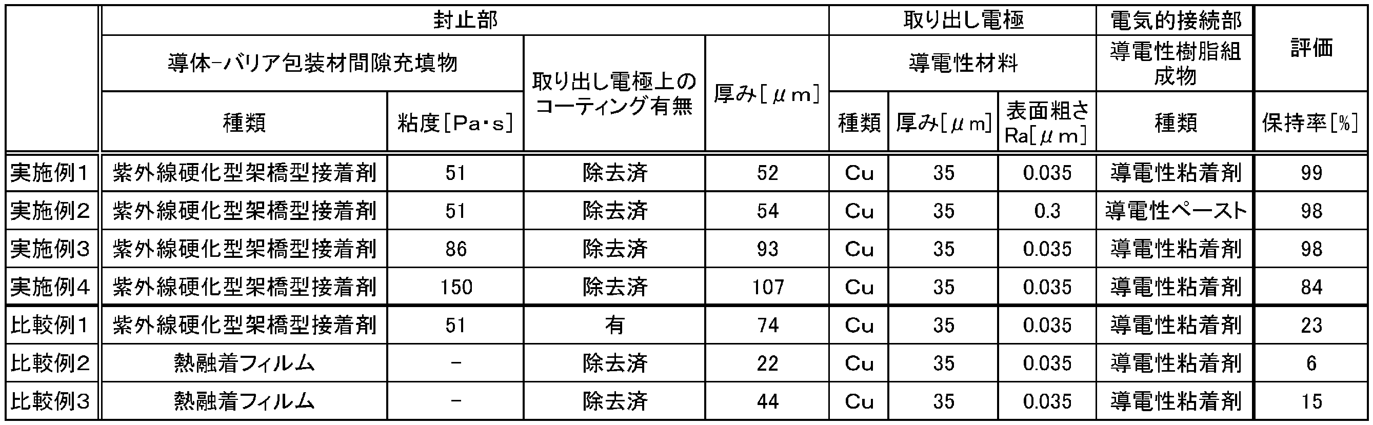
2 光電極
3 第1基板
4 電解質層
5 第2基材
6 対向電極
7 第2基板
8 隔壁
9 セル接続部
11A 第1取り出し電極
11B 第2取り出し電極
12A 第1電気的接続部
12B 第2電気的接続部
13A,13B バリア包装材
14 封止部
15 硬化状態の架橋型接着剤組成物
21 光電極用導電層
22 多孔質半導体微粒子層
61 対向電極用導電層
62 触媒層
91 配線
92 導電性樹脂組成物
100 太陽電池モジュール
Claims (14)
- 第1基板側の第1電極と、第2基板側の第2電極とが、機能層を介して対向してなる1つ又は複数の光電変換セルと、
封止部により封止されて、前記1つ又は複数の光電変換セルを包含する少なくとも1つのバリア包装材と、
前記第1電極に第1電気的接続部を介して接続する第1取り出し電極、及び前記第2電極に第2電気的接続部を介して接続する第2取り出し電極とを備える太陽電池モジュールであって、
前記第1及び第2取り出し電極はそれぞれ導体を含んでなり、
前記バリア包装材は、前記第1取り出し電極及び/又は前記第2取り出し電極を前記太陽電池モジュールから延出させる少なくとも一つの封止部を有し、前記少なくとも一つの封止部で、前記各導体と、前記バリア包装材との間の間隙が、架橋型接着剤組成物の硬化物で充填されてなる、
太陽電池モジュール。 - 前記第1及び第2基板が樹脂フィルムを備える、請求項1に記載の太陽電池モジュール。
- 前記第1及び第2電気的接続部が、導電性樹脂を含む、請求項1又は2に記載の太陽電池モジュール。
- 前記第1及び第2電気的接続部が、はんだを含む、請求項1又は2に記載の太陽電池モジュール。
- 前記架橋型接着剤組成物が、光硬化性樹脂組成物である、請求項1~4の何れかに記載の太陽電池モジュール。
- 前記少なくとも一つの封止部の厚みが、1μm以上250μm以下である、請求項1~5の何れかに記載の太陽電池モジュール。
- 前記第1基板及び/又は第2基板と、前記バリア包装材との間隙の少なくとも一部に接着層を備える、請求項1~6の何れかに記載の太陽電池モジュール。
- 前記機能層が電解質層であり、前記太陽電池モジュールが色素増感型太陽電池モジュールである、請求項1~7の何れかに記載の太陽電池モジュール。
- 請求項1~8の何れかに記載の太陽電池モジュールの製造方法であって、
前記バリア包装材に対して前記架橋型接着剤組成物を塗布する塗布工程と、
前記第1取り出し電極を備える前記第1基板と、前記第2取り出し電極を備える前記第2基板とを有する一対の基板を、前記バリア包装材により上下面から挟む挟み込み工程と、
押圧部材により、前記バリア包装材を介して前記一対の基板を厚み方向に押圧しつつ、前記バリア包装材と、前記第1及び第2取り出し電極の各導体とを前記架橋型接着剤組成物を介して密着させる押圧密着工程と、
を含み、
前記押圧部材は、少なくとも押圧状態にて、前記一対の基板に嵌合する凹部を有する、太陽電池モジュールの製造方法。 - 前記押圧部材が弾性体である、請求項9に記載の太陽電池モジュールの製造方法。
- 前記押圧部材は、前記一対の基板に当接する領域における硬度より、それ以外の領域の硬度が高い、請求項10に記載の太陽電池モジュールの製造方法。
- 前記押圧部材は、非押圧状態で、前記一対の基板に嵌合する凹部を有する、請求項10又は11に記載の太陽電池モジュールの製造方法。
- 前記架橋型接着剤組成物の粘度が10Pa・s以上200Pa・s以下である、請求項9~12の何れかに記載の太陽電池モジュールの製造方法。
- 前記第1電気的接続部の形成材料が予め部分的に配置された第1取り出し電極と、前記第2電気的接続部の形成材料が予め部分的に配置された前記第2取り出し電極と、を用いる、請求項9~13の何れかに記載の太陽電池モジュールの製造方法。
Priority Applications (5)
| Application Number | Priority Date | Filing Date | Title |
|---|---|---|---|
| US16/319,562 US20200006584A1 (en) | 2016-08-02 | 2017-07-31 | Solar cell module and method of producing solar cell module |
| JP2018531895A JP6954287B2 (ja) | 2016-08-02 | 2017-07-31 | 太陽電池モジュール及び太陽電池モジュールの製造方法 |
| EP17836926.0A EP3496120B1 (en) | 2016-08-02 | 2017-07-31 | Solar cell module, and method for producing solar cell module |
| CN201780045636.XA CN109478468B (zh) | 2016-08-02 | 2017-07-31 | 太阳能电池模块及太阳能电池模块的制造方法 |
| KR1020197001970A KR20190030695A (ko) | 2016-08-02 | 2017-07-31 | 태양 전지 모듈 및 태양 전지 모듈의 제조 방법 |
Applications Claiming Priority (2)
| Application Number | Priority Date | Filing Date | Title |
|---|---|---|---|
| JP2016-152172 | 2016-08-02 | ||
| JP2016152172 | 2016-08-02 |
Publications (1)
| Publication Number | Publication Date |
|---|---|
| WO2018025821A1 true WO2018025821A1 (ja) | 2018-02-08 |
Family
ID=61073722
Family Applications (1)
| Application Number | Title | Priority Date | Filing Date |
|---|---|---|---|
| PCT/JP2017/027775 Ceased WO2018025821A1 (ja) | 2016-08-02 | 2017-07-31 | 太陽電池モジュール及び太陽電池モジュールの製造方法 |
Country Status (7)
| Country | Link |
|---|---|
| US (1) | US20200006584A1 (ja) |
| EP (1) | EP3496120B1 (ja) |
| JP (1) | JP6954287B2 (ja) |
| KR (1) | KR20190030695A (ja) |
| CN (1) | CN109478468B (ja) |
| TW (1) | TW201830753A (ja) |
| WO (1) | WO2018025821A1 (ja) |
Cited By (3)
| Publication number | Priority date | Publication date | Assignee | Title |
|---|---|---|---|---|
| CN111477749A (zh) * | 2020-06-03 | 2020-07-31 | 杭州纤纳光电科技有限公司 | 一种轻质光伏组件及封装系统和封装方法 |
| JP2021040114A (ja) * | 2019-09-05 | 2021-03-11 | 日本ゼオン株式会社 | 太陽電池モジュール、太陽電池用電極基板および太陽電池モジュールの製造方法 |
| CN115349156A (zh) * | 2020-04-17 | 2022-11-15 | 埃塞格制造有限公司 | 光伏装置 |
Families Citing this family (4)
| Publication number | Priority date | Publication date | Assignee | Title |
|---|---|---|---|---|
| US11696457B2 (en) | 2018-09-14 | 2023-07-04 | Epishine Ab | Solar cell lamination |
| CN112789728B (zh) * | 2019-02-18 | 2024-04-12 | 爱普施恩有限公司 | 太阳能电池层压 |
| CN115799047B (zh) * | 2021-09-10 | 2025-12-09 | 隆基绿能科技股份有限公司 | 一种薄膜掩膜 |
| CN116528603B (zh) * | 2023-05-31 | 2024-06-11 | 广州追光科技有限公司 | 一种有机太阳能电池及其制备方法 |
Citations (5)
| Publication number | Priority date | Publication date | Assignee | Title |
|---|---|---|---|---|
| JP2008186763A (ja) * | 2007-01-31 | 2008-08-14 | Fujimori Kogyo Co Ltd | 色素増感型太陽電池パネルシート及びその製造方法 |
| WO2009144899A1 (ja) * | 2008-05-27 | 2009-12-03 | 株式会社フジクラ | 光電変換素子 |
| JP2011076727A (ja) * | 2009-09-29 | 2011-04-14 | Fujikura Ltd | 光電変換素子 |
| WO2012111781A1 (ja) * | 2011-02-18 | 2012-08-23 | ソニー株式会社 | 光電変換装置及びその製造方法 |
| JP2015082367A (ja) * | 2013-10-22 | 2015-04-27 | ウシオ電機株式会社 | 色素増感型太陽電池 |
Family Cites Families (6)
| Publication number | Priority date | Publication date | Assignee | Title |
|---|---|---|---|---|
| JP5106876B2 (ja) * | 2007-01-31 | 2012-12-26 | 藤森工業株式会社 | 色素増感型太陽電池モジュール及びその製造方法 |
| JP2009146625A (ja) * | 2007-12-12 | 2009-07-02 | Sony Corp | 色素増感光電変換素子モジュールおよびその製造方法ならびに光電変換素子モジュールおよびその製造方法ならびに電子機器 |
| JP5346932B2 (ja) * | 2008-05-30 | 2013-11-20 | 株式会社フジクラ | 光電変換素子モジュール、及び、光電変換素子モジュールの製造方法 |
| CN101763951B (zh) * | 2008-12-26 | 2012-05-23 | 财团法人工业技术研究院 | 染料敏化电池的封装机台 |
| DE102009020172A1 (de) * | 2009-05-07 | 2010-11-11 | Robert Bürkle GmbH | Presse zum Laminieren von im Wesentlichen plattenförmigen Werkstücken |
| DE102014204125B4 (de) * | 2014-03-06 | 2018-09-13 | Solibro Hi-Tech Gmbh | Laminiervorrichtung und Verfahren zur Herstellung eines Laminats |
-
2017
- 2017-07-31 JP JP2018531895A patent/JP6954287B2/ja active Active
- 2017-07-31 US US16/319,562 patent/US20200006584A1/en not_active Abandoned
- 2017-07-31 CN CN201780045636.XA patent/CN109478468B/zh active Active
- 2017-07-31 EP EP17836926.0A patent/EP3496120B1/en active Active
- 2017-07-31 WO PCT/JP2017/027775 patent/WO2018025821A1/ja not_active Ceased
- 2017-07-31 KR KR1020197001970A patent/KR20190030695A/ko not_active Withdrawn
- 2017-08-02 TW TW106126064A patent/TW201830753A/zh unknown
Patent Citations (5)
| Publication number | Priority date | Publication date | Assignee | Title |
|---|---|---|---|---|
| JP2008186763A (ja) * | 2007-01-31 | 2008-08-14 | Fujimori Kogyo Co Ltd | 色素増感型太陽電池パネルシート及びその製造方法 |
| WO2009144899A1 (ja) * | 2008-05-27 | 2009-12-03 | 株式会社フジクラ | 光電変換素子 |
| JP2011076727A (ja) * | 2009-09-29 | 2011-04-14 | Fujikura Ltd | 光電変換素子 |
| WO2012111781A1 (ja) * | 2011-02-18 | 2012-08-23 | ソニー株式会社 | 光電変換装置及びその製造方法 |
| JP2015082367A (ja) * | 2013-10-22 | 2015-04-27 | ウシオ電機株式会社 | 色素増感型太陽電池 |
Non-Patent Citations (1)
| Title |
|---|
| See also references of EP3496120A4 * |
Cited By (6)
| Publication number | Priority date | Publication date | Assignee | Title |
|---|---|---|---|---|
| JP2021040114A (ja) * | 2019-09-05 | 2021-03-11 | 日本ゼオン株式会社 | 太陽電池モジュール、太陽電池用電極基板および太陽電池モジュールの製造方法 |
| JP7415383B2 (ja) | 2019-09-05 | 2024-01-17 | 日本ゼオン株式会社 | 太陽電池モジュール、太陽電池用電極基板および太陽電池モジュールの製造方法 |
| CN115349156A (zh) * | 2020-04-17 | 2022-11-15 | 埃塞格制造有限公司 | 光伏装置 |
| CN115349156B (zh) * | 2020-04-17 | 2023-08-15 | 埃塞格制造有限公司 | 光伏装置 |
| US12062500B2 (en) | 2020-04-17 | 2024-08-13 | Exeger Operations Ab | Photovoltaic device |
| CN111477749A (zh) * | 2020-06-03 | 2020-07-31 | 杭州纤纳光电科技有限公司 | 一种轻质光伏组件及封装系统和封装方法 |
Also Published As
| Publication number | Publication date |
|---|---|
| EP3496120A1 (en) | 2019-06-12 |
| EP3496120B1 (en) | 2023-05-03 |
| CN109478468B (zh) | 2021-06-08 |
| KR20190030695A (ko) | 2019-03-22 |
| JPWO2018025821A1 (ja) | 2019-05-30 |
| TW201830753A (zh) | 2018-08-16 |
| CN109478468A (zh) | 2019-03-15 |
| JP6954287B2 (ja) | 2021-10-27 |
| US20200006584A1 (en) | 2020-01-02 |
| EP3496120A4 (en) | 2020-05-06 |
Similar Documents
| Publication | Publication Date | Title |
|---|---|---|
| JP6897683B2 (ja) | 太陽電池モジュール | |
| JP6954287B2 (ja) | 太陽電池モジュール及び太陽電池モジュールの製造方法 | |
| JP6958559B2 (ja) | 太陽電池モジュール | |
| JP6897682B2 (ja) | 太陽電池モジュール | |
| JP7567781B2 (ja) | 太陽電池モジュール | |
| JP7415383B2 (ja) | 太陽電池モジュール、太陽電池用電極基板および太陽電池モジュールの製造方法 | |
| CN108231421B (zh) | 染料敏化光伏型电池、模块及其制造方法 | |
| JP2020088234A (ja) | 太陽電池モジュール、太陽電池用電極基板及び太陽電池モジュールの製造方法 |
Legal Events
| Date | Code | Title | Description |
|---|---|---|---|
| WWE | Wipo information: entry into national phase |
Ref document number: 2018531895 Country of ref document: JP |
|
| 121 | Ep: the epo has been informed by wipo that ep was designated in this application |
Ref document number: 17836926 Country of ref document: EP Kind code of ref document: A1 |
|
| ENP | Entry into the national phase |
Ref document number: 20197001970 Country of ref document: KR Kind code of ref document: A |
|
| NENP | Non-entry into the national phase |
Ref country code: DE |
|
| ENP | Entry into the national phase |
Ref document number: 2017836926 Country of ref document: EP Effective date: 20190304 |