WO2018042785A1 - 距離センサ及び距離画像センサ - Google Patents
距離センサ及び距離画像センサ Download PDFInfo
- Publication number
- WO2018042785A1 WO2018042785A1 PCT/JP2017/020055 JP2017020055W WO2018042785A1 WO 2018042785 A1 WO2018042785 A1 WO 2018042785A1 JP 2017020055 W JP2017020055 W JP 2017020055W WO 2018042785 A1 WO2018042785 A1 WO 2018042785A1
- Authority
- WO
- WIPO (PCT)
- Prior art keywords
- region
- transfer
- charge
- image sensor
- main surface
- Prior art date
- Legal status (The legal status is an assumption and is not a legal conclusion. Google has not performed a legal analysis and makes no representation as to the accuracy of the status listed.)
- Ceased
Links
Images


Classifications
-
- H—ELECTRICITY
- H10—SEMICONDUCTOR DEVICES; ELECTRIC SOLID-STATE DEVICES NOT OTHERWISE PROVIDED FOR
- H10F—INORGANIC SEMICONDUCTOR DEVICES SENSITIVE TO INFRARED RADIATION, LIGHT, ELECTROMAGNETIC RADIATION OF SHORTER WAVELENGTH OR CORPUSCULAR RADIATION
- H10F39/00—Integrated devices, or assemblies of multiple devices, comprising at least one element covered by group H10F30/00, e.g. radiation detectors comprising photodiode arrays
- H10F39/10—Integrated devices
- H10F39/12—Image sensors
- H10F39/199—Back-illuminated image sensors
-
- G—PHYSICS
- G01—MEASURING; TESTING
- G01S—RADIO DIRECTION-FINDING; RADIO NAVIGATION; DETERMINING DISTANCE OR VELOCITY BY USE OF RADIO WAVES; LOCATING OR PRESENCE-DETECTING BY USE OF THE REFLECTION OR RERADIATION OF RADIO WAVES; ANALOGOUS ARRANGEMENTS USING OTHER WAVES
- G01S17/00—Systems using the reflection or reradiation of electromagnetic waves other than radio waves, e.g. lidar systems
- G01S17/88—Lidar systems specially adapted for specific applications
- G01S17/89—Lidar systems specially adapted for specific applications for mapping or imaging
-
- G—PHYSICS
- G01—MEASURING; TESTING
- G01S—RADIO DIRECTION-FINDING; RADIO NAVIGATION; DETERMINING DISTANCE OR VELOCITY BY USE OF RADIO WAVES; LOCATING OR PRESENCE-DETECTING BY USE OF THE REFLECTION OR RERADIATION OF RADIO WAVES; ANALOGOUS ARRANGEMENTS USING OTHER WAVES
- G01S7/00—Details of systems according to groups G01S13/00, G01S15/00, G01S17/00
- G01S7/48—Details of systems according to groups G01S13/00, G01S15/00, G01S17/00 of systems according to group G01S17/00
- G01S7/481—Constructional features, e.g. arrangements of optical elements
-
- G—PHYSICS
- G01—MEASURING; TESTING
- G01S—RADIO DIRECTION-FINDING; RADIO NAVIGATION; DETERMINING DISTANCE OR VELOCITY BY USE OF RADIO WAVES; LOCATING OR PRESENCE-DETECTING BY USE OF THE REFLECTION OR RERADIATION OF RADIO WAVES; ANALOGOUS ARRANGEMENTS USING OTHER WAVES
- G01S7/00—Details of systems according to groups G01S13/00, G01S15/00, G01S17/00
- G01S7/48—Details of systems according to groups G01S13/00, G01S15/00, G01S17/00 of systems according to group G01S17/00
- G01S7/483—Details of pulse systems
- G01S7/486—Receivers
- G01S7/4861—Circuits for detection, sampling, integration or read-out
- G01S7/4863—Detector arrays, e.g. charge-transfer gates
-
- H—ELECTRICITY
- H04—ELECTRIC COMMUNICATION TECHNIQUE
- H04N—PICTORIAL COMMUNICATION, e.g. TELEVISION
- H04N25/00—Circuitry of solid-state image sensors [SSIS]; Control thereof
- H04N25/70—SSIS architectures; Circuits associated therewith
-
- H—ELECTRICITY
- H04—ELECTRIC COMMUNICATION TECHNIQUE
- H04N—PICTORIAL COMMUNICATION, e.g. TELEVISION
- H04N25/00—Circuitry of solid-state image sensors [SSIS]; Control thereof
- H04N25/70—SSIS architectures; Circuits associated therewith
- H04N25/76—Addressed sensors, e.g. MOS or CMOS sensors
-
- H—ELECTRICITY
- H10—SEMICONDUCTOR DEVICES; ELECTRIC SOLID-STATE DEVICES NOT OTHERWISE PROVIDED FOR
- H10F—INORGANIC SEMICONDUCTOR DEVICES SENSITIVE TO INFRARED RADIATION, LIGHT, ELECTROMAGNETIC RADIATION OF SHORTER WAVELENGTH OR CORPUSCULAR RADIATION
- H10F39/00—Integrated devices, or assemblies of multiple devices, comprising at least one element covered by group H10F30/00, e.g. radiation detectors comprising photodiode arrays
- H10F39/10—Integrated devices
- H10F39/103—Integrated devices the at least one element covered by H10F30/00 having potential barriers, e.g. integrated devices comprising photodiodes or phototransistors
-
- H—ELECTRICITY
- H10—SEMICONDUCTOR DEVICES; ELECTRIC SOLID-STATE DEVICES NOT OTHERWISE PROVIDED FOR
- H10F—INORGANIC SEMICONDUCTOR DEVICES SENSITIVE TO INFRARED RADIATION, LIGHT, ELECTROMAGNETIC RADIATION OF SHORTER WAVELENGTH OR CORPUSCULAR RADIATION
- H10F39/00—Integrated devices, or assemblies of multiple devices, comprising at least one element covered by group H10F30/00, e.g. radiation detectors comprising photodiode arrays
- H10F39/10—Integrated devices
- H10F39/12—Image sensors
- H10F39/18—Complementary metal-oxide-semiconductor [CMOS] image sensors; Photodiode array image sensors
- H10F39/182—Colour image sensors
-
- H—ELECTRICITY
- H10—SEMICONDUCTOR DEVICES; ELECTRIC SOLID-STATE DEVICES NOT OTHERWISE PROVIDED FOR
- H10F—INORGANIC SEMICONDUCTOR DEVICES SENSITIVE TO INFRARED RADIATION, LIGHT, ELECTROMAGNETIC RADIATION OF SHORTER WAVELENGTH OR CORPUSCULAR RADIATION
- H10F39/00—Integrated devices, or assemblies of multiple devices, comprising at least one element covered by group H10F30/00, e.g. radiation detectors comprising photodiode arrays
- H10F39/80—Constructional details of image sensors
- H10F39/802—Geometry or disposition of elements in pixels, e.g. address-lines or gate electrodes
-
- H—ELECTRICITY
- H10—SEMICONDUCTOR DEVICES; ELECTRIC SOLID-STATE DEVICES NOT OTHERWISE PROVIDED FOR
- H10F—INORGANIC SEMICONDUCTOR DEVICES SENSITIVE TO INFRARED RADIATION, LIGHT, ELECTROMAGNETIC RADIATION OF SHORTER WAVELENGTH OR CORPUSCULAR RADIATION
- H10F39/00—Integrated devices, or assemblies of multiple devices, comprising at least one element covered by group H10F30/00, e.g. radiation detectors comprising photodiode arrays
- H10F39/80—Constructional details of image sensors
- H10F39/803—Pixels having integrated switching, control, storage or amplification elements
- H10F39/8037—Pixels having integrated switching, control, storage or amplification elements the integrated elements comprising a transistor
-
- H—ELECTRICITY
- H10—SEMICONDUCTOR DEVICES; ELECTRIC SOLID-STATE DEVICES NOT OTHERWISE PROVIDED FOR
- H10F—INORGANIC SEMICONDUCTOR DEVICES SENSITIVE TO INFRARED RADIATION, LIGHT, ELECTROMAGNETIC RADIATION OF SHORTER WAVELENGTH OR CORPUSCULAR RADIATION
- H10F39/00—Integrated devices, or assemblies of multiple devices, comprising at least one element covered by group H10F30/00, e.g. radiation detectors comprising photodiode arrays
- H10F39/80—Constructional details of image sensors
- H10F39/805—Coatings
Definitions
- the present invention relates to a distance sensor and a distance image sensor.
- a distance sensor including a silicon substrate and a transfer electrode is known (for example, see Patent Document 1).
- the silicon substrate has a first main surface and a second main surface that face each other.
- a charge generation region in which charges are generated in response to incident light and a charge collection region in which charges from the charge generation region are collected are provided on the first main surface side.
- the transfer electrode is disposed between the charge generation region and the charge collection region on the first main surface. The transfer electrode causes charge to flow from the charge generation region to the charge collection region in accordance with the input signal.
- the distance sensor (distance image sensor) described in Patent Document 1 has room for improvement in spectral sensitivity characteristics in the ultraviolet wavelength band.
- An object of one embodiment of the present invention is to provide a distance sensor and a distance image sensor that are improved in spectral sensitivity characteristics in the ultraviolet wavelength band.
- One embodiment of the present invention is a distance sensor, which includes a silicon substrate and a transfer electrode.
- the silicon substrate has a first main surface and a second main surface that face each other.
- a charge generation region in which charges are generated in response to incident light and a charge collection region in which charges from the charge generation region are collected are provided on the first main surface side.
- the transfer electrode is disposed between the charge generation region and the charge collection region on the first main surface. The transfer electrode causes charge to flow from the charge generation region to the charge collection region in accordance with the input signal.
- a plurality of convex portions are formed in a region corresponding to at least the charge generation region in the second main surface. The plurality of convex portions have slopes inclined with respect to the thickness direction of the silicon substrate. In the convex portion, the (111) plane of the silicon substrate is exposed as a slope.
- the height of the convex part is 200 nm or more.
- the plurality of convex portions formed on the second main surface have slopes inclined with respect to the thickness direction of the silicon substrate.
- the slope is inclined with respect to the thickness direction of the silicon substrate. For this reason, for example, the light reflected on the slope side of one convex part is directed to the slope side of the convex part adjacent to the one convex part, and enters the silicon substrate from the slope of the adjacent convex part.
- the convex portion exposes the (111) plane of the silicon substrate as a slope, light incident on the silicon substrate from the slope is easily taken into the silicon substrate. Since the height of the convex portion is 200 nm or more, the surface area of the slope is large. Therefore, a lot of light incident on the slope is taken into the silicon substrate.
- the light in the ultraviolet wavelength region has a large absorption coefficient by silicon. Therefore, the light in the ultraviolet wavelength region is absorbed in a region near the second main surface of the silicon substrate.
- the (111) plane of the silicon substrate is exposed at the convex portion formed on the silicon substrate. As a result, light absorption in a region close to the second main surface is not hindered.
- the spectral sensitivity characteristics in the ultraviolet wavelength band can be improved.
- the distance sensor according to this aspect may be further provided with a silicon oxide film disposed on the second main surface and transmitting incident light.
- the silicon oxide film functions as an antireflection film, light is more easily captured by the silicon substrate. Therefore, in this embodiment, the spectral sensitivity characteristic in the ultraviolet wavelength band is further improved.
- the distance sensor according to this aspect may be further provided with an aluminum oxide film that is disposed on the second main surface and transmits incident light.
- the fixed charge having a predetermined polarity is present on the light incident surface side of the silicon substrate by the aluminum oxide film.
- a region on the second main surface side of the silicon substrate where a fixed charge of a predetermined polarity exists functions as an accumulation layer.
- the accumulation layer recombines unnecessary charges generated on the second main surface side without depending on light, dark current is reduced.
- the accumulation layer suppresses carriers generated by light near the second main surface of the silicon substrate from being trapped by the second main surface. Therefore, the electric charge generated by light efficiently moves to the first main surface side of the silicon substrate. As a result, according to this embodiment, the light detection sensitivity can be improved.
- the silicon substrate has a first substrate region in which a charge generation region and a charge collection region are provided, and a second substrate region having an impurity concentration higher than that of the first substrate region and provided on the second main surface side. And may have.
- the slope of the convex portion may be included in the surface of the second substrate region.
- the second substrate region functions as an accumulation layer. Therefore, as described above, the light detection sensitivity can be improved.
- the transfer electrode has an annular shape, and may be arranged so as to surround the charge collection region when viewed from a direction orthogonal to the first main surface. In this case, since the charge is transferred from the outside of the transfer electrode to the charge collection region positioned inside the transfer electrode, the charge collection region collects a lot of charges. As a result, in this embodiment, a distance output with a good S / N ratio can be obtained.
- the distance sensor according to the present aspect may be disposed on the second main surface, and may further include a film that transmits incident light and contains boron. In this case, in the distance sensor, deterioration of the spectral sensitivity characteristic in the ultraviolet wavelength band is suppressed.
- the distance image sensor includes a silicon substrate provided with an imaging region including a plurality of units arranged one-dimensionally or two-dimensionally. Each unit is the distance sensor.
- the spectral sensitivity characteristics in the ultraviolet wavelength band can be improved.
- a distance sensor and a distance image sensor that are improved in spectral sensitivity characteristics in the ultraviolet wavelength band.
- FIG. 1 is an explanatory diagram showing the configuration of the distance measuring apparatus.
- FIG. 2 is a schematic diagram illustrating a cross-sectional configuration of the distance image sensor.
- FIG. 3 is a schematic plan view of the distance image sensor.
- FIG. 4 is a diagram illustrating a cross-sectional configuration of each pixel.
- FIG. 5 is a timing chart of various signals.
- FIG. 6 is a schematic diagram showing light travel in the distance image sensor.
- FIG. 7 is an SEM image obtained by observing the distance image sensor according to the first embodiment.
- FIG. 8 is an SEM image obtained by observing the distance image sensor according to the second embodiment.
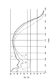
- FIG. 9 is a diagram showing changes in quantum efficiency with respect to wavelength in Examples 1 and 2 and Comparative Example 1.
- FIG. 10 is a diagram showing changes in quantum efficiency with respect to wavelength in Examples 1 and 2 and Comparative Example 1.
- FIG. 11 is a diagram illustrating a cross-sectional configuration of each pixel of a distance image sensor according to a modification.
- FIG. 12 is a diagram illustrating a cross-sectional configuration of each pixel of a distance image sensor according to a modification.
- FIG. 13 is a schematic diagram illustrating a configuration of pixels of a distance image sensor according to a modification.
- FIG. 14 is a diagram illustrating a cross-sectional configuration of each pixel.
- FIG. 15 is a schematic diagram illustrating a configuration of each pixel.
- FIG. 16 is a timing chart of various signals.
- FIG. 11 is a diagram illustrating a cross-sectional configuration of each pixel of a distance image sensor according to a modification.
- FIG. 12 is a diagram illustrating a cross-sectional configuration of each pixel of a distance image sensor according to a modification.
- FIG. 13 is
- FIG. 17 is a schematic diagram illustrating a configuration of pixels of a distance image sensor according to a modification.
- FIG. 18 is a timing chart of various signals.
- FIG. 19 is a diagram illustrating a cross-sectional configuration of each pixel of a distance image sensor according to a modification.
- FIG. 20 is a diagram illustrating a cross-sectional configuration of each pixel of a distance image sensor according to a modification.
- FIG. 21 is a diagram illustrating a cross-sectional configuration of each pixel of a distance image sensor according to a modification.
- FIG. 22 is a diagram illustrating a cross-sectional configuration of each pixel of a distance image sensor according to a modification.
- FIG. 1 is an explanatory diagram showing the configuration of the distance measuring apparatus.
- This distance measuring device includes a distance image sensor 1, a light source 3, a drive circuit 4, a control circuit 2, and an arithmetic circuit 5.
- Drive circuit 4 the light source 3 supplies a drive signal S P.
- the control circuit 2 the distance the first and second transfer electrodes included in each pixel of the image sensor 1: (TX1, TX2 see FIG. 4), the first transfer signal S 1 and the second transfer in synchronization with the drive signal S P give the signal S 2.
- the arithmetic circuit 5 calculates the distance from the signal d ′ (m, n) indicating the distance information read from the first and second semiconductor regions (FD1, FD2: see FIG. 4) of the distance image sensor 1 to the object. Is calculated. Let d be the distance in the horizontal direction D from the distance image sensor 1 to the object.
- the control circuit 2 also outputs third transfer signals S 31 and S 32 described later.
- the drive signal SP, the first transfer signal S 1 , and the second transfer signal S 2 are pulse signals.
- the control circuit 2 has inputs a drive signal S P to the switch 4b of the driving circuit 4.
- the light source 3 is connected to the power source 4a via the switch 4b.
- a drive signal S P is input to the switch 4b, a drive current of the same waveform as the drive signal S P is supplied to the light source 3, it is outputted pulse light L P as a probe light for distance measurement from the light source 3 .
- the pulse light L P When the pulse light L P is irradiated to the object, pulse light is reflected by the object.
- the reflected pulsed light as reflected light L D, enters the range image sensor 1.
- the distance image sensor 1 outputs a detection signal SD .
- the detection signal SD is also a pulse signal.
- the distance image sensor 1 is disposed on the wiring board 10.
- a signal d ′ (m, n) having distance information is output from each pixel of the distance image sensor 1 through the wiring on the wiring board 10.
- the detection signal SD includes a signal d ′ (m, n).
- Waveform of the drive signal S P is a square wave of period T.
- the high level "1", when the low level is "0”, the voltage of the drive signal S P V (t) is given by the following equation.
- V (t) 0 (provided that (T / 2) ⁇ t ⁇ T)
- V (t + T) V (t)
- the first transfer signal S 1 and the second transfer signal S 2 of the waveform is a square wave of period T.
- the first transfer signal S 1 and the second transfer signal S 2 of the voltage V (t) is given by the following equation.
- V (t) 0 (provided that (T / 2) ⁇ t ⁇ T)
- V (t + T) V (t)
- V (t) 1 (provided that (T / 2) ⁇ t ⁇ T)
- V (t + T) V (t)
- Signal S P, S 1, S 2 , S D has all pulse period 2 ⁇ T P.
- the amount of charge generated in the distance image sensor 1 when the first transfer signal S 1 and the detection signal SD are both “1” is defined as q 1 .
- the amount of charge generated in the distance image sensor 1 when the second transfer signal S 2 and the detection signal SD are both “1” is defined as q 2 .
- the phase difference between the first transfer signal S 1 and the detection signal SD is equal to the amount of charge q 2 generated in the distance image sensor 1 during the overlap period in which the second transfer signal S 2 and the detection signal SD are “1”.
- the amount of charge q 2 is the amount of charge generated during a period in which the logical product of the second transfer signal S 2 and the detection signal SD is “1”.
- the arithmetic circuit 5 can calculate the distance d. Note that the above-described pulse is repeatedly emitted, and the integrated value can be output as the respective charge amounts q 1 and q 2 .
- the ratio of the charge amounts q 1 and q 2 to the total charge amount corresponds to the above-described phase difference, that is, the distance to the object.
- a coefficient ⁇ for correcting the latter may be obtained in advance.
- a value obtained by multiplying the calculated distance d by the coefficient ⁇ may be the final calculated distance d.
- the light speed c differs according to the outside air temperature
- the outside air temperature may be measured and the light speed c may be corrected based on the outside air temperature.
- distance calculation may be performed based on the corrected light velocity c.
- the relationship between the signal input to the arithmetic circuit and the actual distance may be stored in advance in the memory.
- the distance calculation may be performed by a lookup table method.
- the calculation method may be changed according to the sensor structure. In this case, a conventionally known calculation method may be used.
- FIG. 2 is a schematic diagram for illustrating a cross-sectional configuration of the distance image sensor.
- the distance image sensor 1 is a back-illuminated distance image sensor and includes a semiconductor substrate 1A. In the present embodiment, the entire semiconductor substrate 1A is thinned.
- the range image sensor 1 the reflected light L D from the light incident surface 1BK of the semiconductor substrate 1A is incident.
- the light incident surface 1BK is the back surface of the semiconductor substrate 1A.
- a surface 1FT of the distance image sensor 1 is connected to the wiring substrate 10 via an adhesion region AD.
- the adhesion region AD is a region including an adhesion element such as a bump electrode.
- the adhesion region AD has an electrically insulating adhesive or filler as necessary.
- FIG. 3 is a schematic plan view of the distance image sensor.
- the semiconductor substrate 1A has an imaging region 1B.
- the imaging region 1B has a plurality of pixels P (m, n) that are arranged two-dimensionally. From each pixel P (m, n), two charge amounts (q 1 , q 2 ) are output as the signal d ′ (m, n) having the above-described distance information. That is, each pixel P (m, n) outputs a signal d ′ (m, n) corresponding to the distance to the object. Each pixel P (m, n) functions as a minute distance measuring sensor. When reflected light from the object is imaged on the imaging region 1B, a distance image of the object can be obtained. The distance image of the object is a collection of distance information to each point on the object.
- One pixel P (m, n) functions as one distance sensor (unit).
- the distance image sensor 1 includes a plurality of units (a plurality of distance sensors).
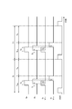
- FIG. 4 is a diagram showing a cross-sectional configuration of each pixel of the distance image sensor.
- the distance image sensor 1 includes a semiconductor substrate 1A, a photogate electrode PG, a first transfer electrode TX1, and a second transfer electrode TX2.
- the semiconductor substrate 1A has a light incident surface 1BK (second main surface) and a surface 1FT (first main surface) that face each other.
- the semiconductor substrate 1A is a silicon substrate.
- the photogate electrode PG is disposed on the surface 1FT.
- the first transfer electrode TX1 and the second transfer electrode TX2 are disposed on the surface 1FT and are adjacent to the photogate electrode PG.
- An insulating layer 1E is arranged on the surface 1FT.
- the surface 1FT is in contact with the insulating layer 1E.
- the insulating layer 1E is located between the surface 1FT, the photogate electrode PG, the first transfer electrode TX1, and the second transfer electrode TX2.
- the photogate electrode PG, the first transfer electrode TX1, and the second transfer electrode TX2 are in contact with the insulating layer 1E.
- the photogate electrode PG is located between the first transfer electrode TX1 and the second transfer electrode TX2 when viewed from the direction orthogonal to the surface 1FT.
- a first semiconductor region FD1 and a second semiconductor region FD2 are provided on the surface 1FT side of the semiconductor substrate 1A.
- the first semiconductor region FD1 collects charges flowing into a region immediately below the first transfer electrode TX1.
- the first semiconductor region FD1 accumulates the flowed-in charges as signal charges.
- the second semiconductor region FD2 collects charges flowing into the region immediately below the second transfer electrode TX2.
- the second semiconductor region FD2 accumulates the flowed-in charges as signal charges.
- the first semiconductor region FD1 and the second semiconductor region FD2 function as signal charge collection regions.
- the photogate electrode PG has, for example, a rectangular shape in plan view.
- a region corresponding to the photogate electrode PG in the semiconductor substrate 1A (a region immediately below the photogate electrode PG in the semiconductor substrate 1A) functions as a charge generation region (photosensitive region) in which charges are generated according to incident light.
- the photogate electrode PG is made of polysilicon, for example.
- the photogate electrode PG may be made of a material other than polysilicon.
- the photogate electrode PG, the first transfer electrode TX1, and the second transfer electrode TX2 are located between the first semiconductor region FD1 and the second semiconductor region FD2 when viewed from the direction orthogonal to the surface 1FT.
- the first transfer electrode TX1 is located between the photogate electrode PG and the first semiconductor region FD1 when viewed from the direction orthogonal to the surface 1FT.
- the second transfer electrode TX2 is located between the photogate electrode PG and the second semiconductor region FD2 when viewed from the direction orthogonal to the surface 1FT.
- the first semiconductor region FD1 and the second semiconductor region FD2 are separated from the photogate electrode PG.
- the first semiconductor region FD1 and the second semiconductor region FD2 are opposed to each other through the photogate electrode PG.
- the first semiconductor region FD1 is adjacent to a region immediately below the first transfer electrode TX1 in the semiconductor substrate 1A.
- the second semiconductor region FD2 is adjacent to a region immediately below the second transfer electrode TX2 in the semiconductor substrate 1A.
- the first transfer electrode TX1 causes the charge generated in the charge generation region to flow into the first semiconductor region FD1 in response to the first transfer signal S 1 (see FIG. 5).
- the charge flowing into the first semiconductor region FD1 is treated as a signal charge.
- Second transfer electrode TX2 according to the first transfer signals S 1 and the second phase have different transfer signal S 2 (see FIG. 5), the second semiconductor region FD2 charges generated at the charge generation region as signal charges Let it flow.
- the charge flowing into the second semiconductor region FD2 is treated as a signal charge.
- the first transfer electrode TX1 and the second transfer electrode TX2 have, for example, a rectangular shape in plan view.
- the length of the first transfer electrode TX1 is equal to the length of the second transfer electrode TX2.
- the first transfer electrode TX1 and the second transfer electrode TX2 are made of, for example, polysilicon.
- the first transfer electrode TX1 and the second transfer electrode TX2 may be made of a material other than polysilicon.
- the first transfer electrode TX1 and the second transfer electrode TX2 function as signal charge transfer electrodes.
- the semiconductor substrate 1A is, for example, a silicon substrate having a low impurity concentration and made of a p-type semiconductor.
- the first semiconductor region FD1 and the second semiconductor region FD2 are regions having a high impurity concentration and made of an n-type semiconductor.
- the first semiconductor region FD1 and the second semiconductor region FD2 are floating diffusion regions.
- the thickness of the semiconductor substrate 1A is, for example, 3 to 100 ⁇ m.
- the impurity concentration of the semiconductor substrate 1A is, for example, 1 ⁇ 10 12 to 10 15 cm ⁇ 3 .
- the thickness of the first and second semiconductor regions FD1, FD2 is, for example, 0.1 to 0.5 ⁇ m.
- the impurity concentration of the first and second semiconductor regions FD1, FD2 is, for example, 1 ⁇ 10 18 to 10 20 cm ⁇ 3 .
- the insulating layer 1E is provided with contact holes that expose the surfaces of the first semiconductor region FD1 and the second semiconductor region FD2.
- a conductor 11 for electrically connecting the first semiconductor region FD1 and the second semiconductor region FD2 to the outside is disposed in the contact hole.
- Insulating layer 1E for example, made of SiO 2.
- the second transfer signal S 2 of the phase applied to the first transfer signals S 1 and the phase of the second transfer electrode TX2 applied to the first transfer electrode TX1, are 180 degrees.
- the light incident on the pixel P (m, n) is converted into electric charge in the semiconductor substrate 1A.
- a part of the generated charges is, as a signal charge, in the direction of the first transfer electrode TX1 or according to the potential gradient formed by the voltage applied to the photogate electrode PG and the first and second transfer electrodes TX1 and TX2. Travels in the direction of the second transfer electrode TX2.
- a high level signal for example, positive potential
- the potential below the first transfer electrode TX1 is below the photogate electrode PG. It becomes lower than the potential of the partial semiconductor substrate 1A. Therefore, electrons are drawn in the direction of the first transfer electrode TX1 and accumulated in the potential well formed by the first semiconductor region FD1. That is, charges generated in the semiconductor substrate 1A are collected in the first semiconductor region FD1.
- An n-type semiconductor includes a positively ionized donor, has a positive potential, and attracts electrons.
- a potential for example, ground potential
- a potential barrier is generated by the first transfer electrode TX1. Therefore, the charge generated in the semiconductor substrate 1A is not drawn into the first semiconductor region FD1, and is not collected in the first semiconductor region FD1.
- a high level signal for example, positive potential
- the potential below the second transfer electrode TX2 is below the photogate electrode PG. It becomes lower than the potential of the partial semiconductor substrate 1A. Accordingly, electrons are drawn in the direction of the second transfer electrode TX2 and accumulated in the potential well formed by the second semiconductor region FD2. That is, charges generated in the semiconductor substrate 1A are collected in the second semiconductor region FD2.
- a potential for example, a ground potential
- a potential barrier is generated by the second transfer electrode TX2. Accordingly, the charges generated in the semiconductor substrate 1A are not drawn into the second semiconductor region FD2, and are not collected in the second semiconductor region FD2.
- FIG. 5 is a timing chart of various signals.
- the two frame period T F consecutive in time series is illustrated.
- the drive signal S P the intensity signal S Lr of the light source 3, the first transfer signal S 1 applied to the first transfer electrode TX1, the second transfer signal S 2 applied to the second transfer electrode TX2, And a reset signal reset is shown.
- Intensity signal S Lr is the intensity signal of the reflected light L D when reflected light L D is back to the imaging region 1B.
- Each of the two frame periods TF includes a period for accumulating signal charges (accumulation period) T acc and a period for reading signal charges (readout period) Tro .
- Drive signal S P, the intensity signal S Lr, first transfer signal S 1, and the second transfer signal S 2 are both pulse signal having a pulse width T P.
- a reset signal reset is applied to the first semiconductor region FD1 and the second semiconductor region FD2.
- the drive signal SP is applied to the light source 3.
- the drive signal S P it is applied to the first transfer signals S 1 and the second transfer signal S 2 in the reverse phase to each other first transfer electrode TX1 and the second transfer electrode TX2.
- the application of the first transfer signals S 1 and the second transfer signal S 2 the charge transfer is performed.
- signal charges are collected in the first semiconductor region FD1 and the second semiconductor region FD2.
- the readout period T ro collected signal charges in the first semiconductor region FD1 and the second semiconductor region FD2 is read.
- the first transfer signal S 1 is output in synchronization with the drive signal SP with a phase difference of 0, and the second transfer signal S 2 is synchronized with the drive signal SP with a phase difference of 180 degrees. Is output. Output control of the first transfer signal S 1 and the second transfer signal S 2 is performed by the control circuit 2.
- Control circuit 2 in synchronization with the emission of the pulse light L P, for each frame period T F, so as to flow into the first semiconductor region FD1 charges generated at the charge generation region as the signal charge, the first transfer outputs signals S 1 to the first transfer electrodes TX1, so as to flow into the second semiconductor region FD2 charges generated at the charge generation region as the signal charge, the first transfer signals S 1 and the phase is different second transfer signal and it outputs the S 2 to the second transfer electrode TX2.
- intensity signal S Lr the driving signal S charge quantity q 1 of P to correspond to overlapping portions of the first transfer signals S 1 to be output in synchronization with the phase difference 0 is collected in the first semiconductor region FD1 .
- intensity signal S Lr of the reflected light L D the charge amount q 2 corresponding to overlapping portions of the second transfer signal S 2 to be synchronized and output at a phase difference of 180 to the drive signal S P, the second semiconductor region Collected in FD2.
- phase difference Td is from the range image sensor 1 to the object Represents the distance d.
- the distance d is calculated by the calculation circuit 5 using the ratio of the charge amount q 1 and the charge amount q 2 in one frame period TF according to the following equation (1).
- C is the speed of light.
- the arithmetic circuit 5 reads out the charge amounts q 1 and q 2 of the signal charges collected in the first semiconductor region FD1 and the second semiconductor region FD2 for each frame period TF .
- the arithmetic circuit 5 calculates the distance d to the object based on the read charge amounts q 1 and q 2 .
- a plurality of convex portions 20 are formed on the light incident surface 1BK of the semiconductor substrate 1A.
- the plurality of convex portions 20 are formed in the entire imaging region 1B on the light incident surface 1BK.
- the plurality of convex portions 20 may be formed only in a region corresponding to the charge generation region in the semiconductor substrate 1A. That is, the plurality of convex portions 20 may be formed only in a region corresponding to the photogate electrode PG in the semiconductor substrate 1A.
- Each convex portion 20 has a substantially pyramid shape, and has a slope 20a inclined with respect to the thickness direction of the semiconductor substrate 1A.
- the convex portion 20 has, for example, a substantially quadrangular pyramid shape.
- the height of the convex part 20 is 200 nm or more.
- the distance between the apexes of the two adjacent convex portions 20 is, for example, 500 to 3000 nm.
- the (111) plane of the semiconductor substrate 1A is exposed as the inclined surface 20a.
- the slope 20a is optically exposed.
- the fact that the inclined surface 20a is optically exposed includes not only the case where the inclined surface 20a is in contact with atmospheric gas such as air, but also the case where an optically transparent film is formed on the inclined surface 20a.
- the distance image sensor 1 includes an antireflection film 21.
- the antireflection film 21 is disposed on the light incident surface 1BK of the semiconductor substrate 1A.
- the antireflection film 21 is a silicon oxide (SiO 2 ) film. That is, the antireflection film 21 is an oxide film that transmits incident light.
- the antireflection film 21 is in contact with the inclined surface 20 a so as to cover the inclined surface 20 a of the convex portion 20. Concavities and convexities corresponding to the plurality of convex portions 20 are formed on the surface of the antireflection film 21.
- the thickness of the antireflection film 21 is, for example, 1 to 200 nm.
- the plurality of convex portions 20 formed on the light incident surface 1BK have the inclined surfaces 20a. If the reflected light L D is made incident from the light incident surface 1BK into the semiconductor substrate 1A, as shown in FIG. 6, part of the light is reflected by the light incident surface 1BK side. Since the inclined surface 20a is inclined with respect to the thickness direction of the semiconductor substrate 1A, for example, the light reflected on the inclined surface 20a side of one convex portion 20 is the inclined surface 20a of the convex portion 20 adjacent to the one convex portion 20. The light is incident on the semiconductor substrate 1 ⁇ / b> A from the inclined surface 20 a of the convex portion 20 that is directed toward the side. That is, the light reflected on the light incident surface 1BK (slope 20a) side is incident on the semiconductor substrate 1A again.
- the (111) plane of the semiconductor substrate 1A is exposed as the inclined surface 20a. Therefore, light incident on the semiconductor substrate 1A from the inclined surface 20a is easily taken into the semiconductor substrate 1A. Since the height of the convex part 20 is 200 nm or more, the surface area of the slope 20a is large. Therefore, a lot of light incident on the inclined surface 20a is taken into the semiconductor substrate 1A.
- the light in the ultraviolet wavelength region has a large absorption coefficient by silicon. Therefore, light in the ultraviolet wavelength region is absorbed in a region near the light incident surface 1BK (slope 20a) in the semiconductor substrate 1A. In the distance image sensor 1, the (111) surface of the semiconductor substrate 1A is exposed at the convex portion 20 formed on the semiconductor substrate 1A. Therefore, light absorption in a region close to the light incident surface 1BK is not hindered.
- the range image sensor 1 has improved spectral sensitivity characteristics in the ultraviolet wavelength band.
- the distance image sensor 1 is also improved in spectral sensitivity characteristics in the near-infrared wavelength band.
- the light L D 1 that has entered the semiconductor substrate 1A from the inclined surface 20a may travel in the direction intersecting the thickness direction of the semiconductor substrate 1A and reach the surface 1FT as shown in FIG. At this time, the light L D 1 reaching the surface 1FT is totally reflected by the surface 1FT depending on the angle reaching the surface 1FT. As a result, the travel distance of the light incident on the distance image sensor 1 (semiconductor substrate 1A) becomes longer.
- the light L D 2 re-entering the semiconductor substrate 1A travels through the semiconductor substrate 1A in a direction intersecting the thickness direction of the semiconductor substrate 1A. Therefore, the traveling distance of the light L D 2 re-entering the distance image sensor 1 (semiconductor substrate 1A) is also increased.
- the distance image sensor 1 can improve spectral sensitivity characteristics in the near-infrared wavelength band.
- the distance image sensor 1 When the distance image sensor 1 is used outdoors, it may be affected by ambient light. When the distance image sensor 1 is affected by disturbance light, the distance accuracy detected by the distance image sensor 1 deteriorates.
- the disturbance light includes, for example, sunlight.
- the intensity of irradiation with sunlight sharply decreases in a wavelength band of about 400 nm or less. Therefore, by using a light source that emits light of a wavelength band of about 400 nm or less as the light source 3, it is possible to suppress the deterioration of the distance accuracy detected by the distance image sensor 1. As described above, the range image sensor 1 is improved in spectral sensitivity characteristics in the ultraviolet wavelength band. Therefore, even if the light source 3 is a light source for emitting light of a wavelength band of about 400 nm, the range image sensor 1 is properly detect the reflected light L D.
- the irradiation intensity of sunlight decreases not only in the wavelength band of about 400 nm or less, but also in the wavelength band near about 940 nm. Therefore, the use of a light source that emits light having a wavelength band near about 940 nm as the light source 3 can also suppress the deterioration of the distance accuracy detected by the distance image sensor 1.
- the distance image sensor 1 has improved spectral sensitivity characteristics even in the near-infrared wavelength band. Therefore, even if the light source 3 is a light source for emitting light in the wavelength band around about 940 nm, the range image sensor 1 is properly detect the reflected light L D.
- the distance image sensor 1 includes an antireflection film 21 that is a silicon oxide film. Therefore, light is more easily taken in by the semiconductor substrate 1A. As a result, the distance image sensor 1 further improves the spectral sensitivity characteristics in the ultraviolet and near-infrared wavelength bands.
- the present inventors conducted an experiment for confirming the effect of improving the spectral sensitivity characteristic according to the present embodiment.
- the distance image sensor 1 (referred to as Examples 1 and 2) having the above-described configuration and the distance image sensor 1 (referred to as Comparative Example 1) in which no convex portion is formed on the light incident surface of the semiconductor substrate are manufactured. Then, the spectral sensitivity characteristics of each distance image sensor 1 were examined. Examples 1 and 2 and Comparative Example 1 have the same configuration except for the formation of convex portions. The size of the charge generation region was set to 0.5 mm ⁇ .
- Example 1 the height of the convex portion 20 is 1570 nm (however, the thickness of the antireflection film 21 is included).
- Example 2 the height of the convex portion 20 is 1180 nm (however, the thickness of the antireflection film 21 is included).
- FIGS. 7 and 8A are SEM images obtained by observing the surface on the light incident surface side of the distance image sensor (the surface of the antireflection film 21) from an oblique angle of 45 °.
- FIG. 7 and FIG. 8B are SEM images obtained by observing the end face of the distance image sensor.
- the spectral sensitivity characteristic of Example 1 is indicated by T1
- the spectral sensitivity characteristic of Example 1 is indicated by T2
- the spectral sensitivity characteristic of Comparative Example 1 is indicated by T3.
- the vertical axis indicates the quantum efficiency (QE)
- the horizontal axis indicates the wavelength (nm) of light.
- FIG. 10 shows spectral sensitivity characteristics in the vacuum ultraviolet wavelength band.
- Example 1 has improved spectral sensitivity characteristics in each wavelength band of ultraviolet and near infrared.
- the distance image sensor 1 includes an aluminum oxide (Al 2 O 3 ) film 23 instead of the antireflection film 21.
- FIG. 11 is a diagram illustrating a cross-sectional configuration of each pixel of the distance image sensor according to the present modification.
- the aluminum oxide film 23 is disposed on the light incident surface 1BK.
- the aluminum oxide film 23 is an oxide film that transmits incident light.
- the thickness of the aluminum oxide film 23 is, for example, 0.0003 to 3 ⁇ m. Concavities and convexities corresponding to the plurality of convex portions 20 are formed on the surface of the aluminum oxide film 23.
- the aluminum oxide film 23 is negatively charged. Since the conductivity type of the semiconductor substrate 1A is p-type, the aluminum oxide film 23 causes a predetermined fixed charge (positive fixed charge) to exist on the light incident surface 1BK side of the semiconductor substrate 1A. The region on the light incident surface 1BK side of the semiconductor substrate 1A where the positive fixed charge exists functions as an accumulation layer. Therefore, the slope 20a of the convex portion 20 is included in the surface of the accumulation layer.
- the unnecessary charge generated without depending on the light on the light incident surface 1BK side is recombined by the accumulation layer, so that dark current is reduced.
- the accumulation layer suppresses charges generated by light near the light incident surface 1BK of the semiconductor substrate 1A from being trapped by the light incident surface 1BK. Therefore, the electric charge generated by light efficiently moves to the surface 1FT side of the semiconductor substrate 1A. As a result, the distance image sensor 1 according to this modification can improve the light detection sensitivity.
- a silicon oxide film may be disposed between the aluminum oxide film 23 and the light incident surface 1BK. That is, the aluminum oxide film 23 may not be in direct contact with the light incident surface 1BK. Even in this case, the aluminum oxide film 23 causes positive fixed charges to exist on the light incident surface 1BK side of the semiconductor substrate 1A.
- the semiconductor substrate 1A includes a first substrate region 1Aa and a second substrate region 1Ab.
- FIG. 12 is a diagram illustrating a cross-sectional configuration of each pixel of the distance image sensor according to the present modification.
- the first substrate region 1Aa is provided on the surface 1FT side of the semiconductor substrate 1A.
- the first substrate region 1Aa includes the surface 1FT.
- the second substrate region 1Ab is provided on the light incident surface 1BK side of the semiconductor substrate 1A.
- the second substrate region 1Ab includes a light incident surface 1BK.
- the first substrate region 1Aa and the second substrate region 1Ab are made of a p-type semiconductor.
- the impurity concentration of the second substrate region 1Ab is higher than the impurity concentration of the first substrate region 1Aa.
- the semiconductor substrate 1A can be obtained, for example, by growing a p ⁇ type epitaxial layer having an impurity concentration lower than that of the semiconductor substrate on the p type semiconductor substrate.
- the first semiconductor region FD1 and the second semiconductor region FD2 are provided in the first substrate region 1Aa.
- the insulating layer 1E is disposed on the surface (front surface 1FT) of the first substrate region 1Aa.
- a plurality of convex portions 20 are formed on the light incident surface 1BK included in the second substrate region 1Ab. That is, the inclined surface 20a of the convex portion 20 is included in the surface (light incident surface 1BK) of the second substrate region 1Ab. In the convex part 20, (111) plane of 2nd board
- the antireflection film 21 is disposed on the surface (light incident surface 1BK) of the second substrate region 1Ab.
- the second substrate region 1Ab functions as an accumulation layer. Therefore, as described above, the distance image sensor 1 according to this modification can improve the light detection sensitivity.
- the distance image sensor 1 according to the modification shown in FIG. 12 may also include an aluminum oxide film 23 instead of the antireflection film 21.
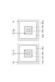
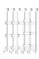
- the distance image sensor 1 includes a plurality of photogate electrodes (two photogate electrodes in this modification) PG1 and PG2 in each pixel P (m, n).
- First transfer electrode TX1 and second transfer electrode TX2 a plurality of third transfer electrodes (two third transfer electrodes in the present embodiment) TX3 1 , TX3 2 , first semiconductor region FD1 and second semiconductor region FD2 and a plurality of third semiconductor regions (in this embodiment, two third semiconductor regions) FD3 1 and FD3 2 are provided.
- FIG. 13 is a schematic diagram for illustrating a configuration of a pixel of a distance image sensor according to this modification.
- FIG. 14 is a diagram illustrating a cross-sectional configuration of each pixel.
- the two photogate electrodes PG1 and PG2 are disposed on the surface 1FT and are separated from each other.
- the first transfer electrode TX1 and the third transfer electrodes TX3 1 is disposed on the surface 1FT, adjacent to the photo gate electrode PG1.
- Second transfer electrode TX2 and the third transfer electrodes TX3 2 is disposed on the surface 1FT, adjacent to the photo gate electrode PG1.
- An insulating layer 1E is arranged on the surface 1FT. The insulating layer 1E is located between the surface 1FT and the photogate electrodes PG1, PG2 and the first to third transfer electrodes TX1, TX2, TX3 1 , TX3 2 .
- the photogate electrodes PG1, PG2 and the first to third transfer electrodes TX1, TX2, TX3 1 , TX3 2 are in contact with the insulating layer 1E.
- the first semiconductor region FD1 collects charges flowing into a region immediately below the first transfer electrode TX1.
- the first semiconductor region FD1 accumulates the flowing charge.
- the second semiconductor region FD2 collects charges flowing into the region immediately below the second transfer electrode TX2.
- the second semiconductor region FD2 accumulates the flowing charge.
- the third semiconductor region FD3 1 collects the charge flowing into the region immediately below the third transfer electrode TX3 1 .
- the third semiconductor region FD3 2 collects the charge flowing into the region immediately below the third transfer electrode TX3 2 .
- the photogate electrodes PG1, PG2 have a substantially annular shape in plan view.
- the photogate electrodes PG1, PG2 have a substantially polygonal ring (for example, a rectangular ring).
- the photogate electrodes PG1 and PG2 may have an annular shape.
- the photogate electrodes PG1, PG2 are made of polysilicon, for example. However, other materials may be used.
- the photogate electrodes PG1 and PG2 may be made of a material other than polysilicon.
- the first semiconductor region FD1 is disposed inside the photogate electrode PG1 so as to be surrounded by the photogate electrode PG1.
- the first semiconductor region FD1 is separated from the region immediately below the photogate electrode PG1.
- the first semiconductor region FD1 is located inside the light receiving region so as to be surrounded by the light receiving region, and is separated from the charge generation region.
- the second semiconductor region FD2 is disposed inside the photogate electrode PG2 so as to be surrounded by the photogate electrode PG2.
- the second semiconductor region FD2 is separated from the region immediately below the photogate electrode PG2.
- the second semiconductor region FD2 is located inside the light receiving region so as to be surrounded by the light receiving region, and is separated from the charge generation region.
- the first semiconductor region FD1 and the second semiconductor region FD2 have a substantially polygonal shape in plan view.
- the first semiconductor region FD1 and the second semiconductor region FD2 have a rectangular shape (for example, a square shape).
- the first transfer electrode TX1 is disposed between the photogate electrode PG1 and the first semiconductor region FD1.
- the first transfer electrode TX1 is located outside the first semiconductor region FD1 so as to surround the first semiconductor region FD1, and is located inside the photogate electrode PG1 so as to be surrounded by the photogate electrode PG1. .
- the first transfer electrode TX1 is located between the photogate electrode PG1 and the first semiconductor region FD1, and is separated from the photogate electrode PG1 and the first semiconductor region FD1.
- the second transfer electrode TX2 is disposed between the photogate electrode PG2 and the second semiconductor region FD2.
- the second transfer electrode TX2 is located outside the second semiconductor region FD2 so as to surround the second semiconductor region FD2, and is located inside the photogate electrode PG2 so as to be surrounded by the photogate electrode PG2. .
- the second transfer electrode TX2 is located between the photogate electrode PG2 and the second semiconductor region FD2, and is separated from the photogate electrode PG2 and the second semiconductor region FD2.
- the first transfer electrode TX1 and the second transfer electrode TX2 have a substantially polygonal shape in plan view.
- the first transfer electrode TX1 and the second transfer electrode TX2 have a rectangular ring shape.
- Third semiconductor region FD3 1 is disposed on the outside of the photo gate electrode PG1 so as to surround the photo gate electrode PG1. Third semiconductor region FD3 1 is spaced apart from the region immediately below the photogate electrode PG1. Third semiconductor region FD3 1 is located outside of the light-receiving region so as to surround the light receiving area is spaced from the charge generation region.
- Third semiconductor region FD3 2 is disposed on the outside of the photo gate electrode PG2 so as to surround the photo gate electrode PG2. Third semiconductor region FD3 2 is spaced apart from the region immediately below the photogate electrode PG2. Third semiconductor region FD3 2 is located outside of the light-receiving region so as to surround the light receiving area is spaced from the charge generation region.
- the third semiconductor regions FD3 1 and FD3 2 have a substantially polygonal shape in plan view.
- the third semiconductor regions FD3 1 and FD3 2 have a rectangular annular shape.
- adjacent third semiconductor regions FD3 1 and FD3 2 are integrally formed. That is, the third semiconductor region FD3 1 and the third semiconductor region FD3 2 share a region between the third transfer electrode TX3 1 and the third transfer electrode TX3 2 .
- the third semiconductor regions FD3 1 and FD3 2 function as unnecessary charge collection regions.
- the third semiconductor regions FD3 1 and FD3 2 are regions having a high impurity concentration and made of an n-type semiconductor.
- the third semiconductor regions FD3 1 and FD3 2 are floating diffusion regions.
- Third transfer electrodes TX3 1 is disposed between the photo gate electrode PG1 and the third semiconductor region FD3 1.
- Third transfer electrodes TX3 1, together are positioned outside of the photo gate electrode PG1 so as to surround the photo gate electrode PG1, positioned in the third inner semiconductor region FD3 1 so as to be surrounded by the third semiconductor region FD3 1 is doing.
- Third transfer electrodes TX3 1 is located between the photo gate electrode PG1 and the third semiconductor region FD3 1, spaced apart from the photo gate electrode PG1 and third semiconductor regions FD3 1.
- Third transfer electrodes TX3 2 is disposed between the photo gate electrode PG2 and the third semiconductor region FD3 2.
- Third transfer electrodes TX3 2 together are positioned outside of the photo gate electrode PG2 so as to surround the photo gate electrode PG2, positioned inside of the third semiconductor region FD3 2 so as to be surrounded by the third semiconductor region FD3 2 is doing.
- Third transfer electrodes TX3 2 is located between the photo gate electrode PG2 and the third semiconductor region FD3 2, it is spaced apart from the photo gate electrode PG2 and the third semiconductor region FD3 2.
- the third transfer electrodes TX3 1 , TX3 2 have a substantially polygonal shape in plan view. In this modification, the third transfer electrodes TX3 1 and TX3 2 have a rectangular ring shape.
- the third transfer electrodes TX3 1 and TX3 2 are made of polysilicon, for example.
- the third transfer electrodes TX3 1 and TX3 2 may be made of a material other than polysilicon.
- the third transfer electrodes TX3 1 and TX3 2 function as unnecessary charge transfer electrodes.
- the insulating layer 1E is provided with contact holes (not shown) exposing the surfaces of the first to third semiconductor regions FD1, FD2, FD3 1 and FD3 2 .
- a conductor (not shown) for electrically connecting the first to third semiconductor regions FD1, FD2, FD3 1 and FD3 2 to the outside is disposed in the contact hole.
- the region corresponding to the photogate electrodes PG1 and PG2 in the semiconductor substrate 1A functions as a charge generation region in which charges are generated according to incident light. Therefore, the charge generation region has a rectangular ring shape corresponding to the shape of the photogate electrodes PG1 and PG2.
- a first unit including a photogate electrode PG1 (a charge generation region immediately below the photogate electrode PG1), and a second unit including a photogate electrode PG2 (a charge generation region immediately below the photogate electrode PG2) Are arranged next to each other.
- the first unit and the second unit arranged adjacent to each other constitute one pixel P (m, n).
- a high-level signal e.g., positive potential
- Negative charges (electrons) are drawn in the direction of the third transfer electrodes TX3 1 and TX3 2 and flow into the potential well formed by the third semiconductor regions FD3 1 and FD3 2 .
- the third semiconductor regions FD3 1 and FD3 2 collect a part of the charges generated in the charge generation region in response to the incidence of light as unnecessary charges and discharge them.
- FIG. 15 is a schematic diagram for illustrating the configuration of each pixel.
- the first transfer electrode TX1, the first transfer signal S 1 is given.
- the second transfer electrodes TX2, the second transfer signal S 2 is applied.
- Third transfer signals S 31 and S 32 are applied to the third transfer electrodes TX 3 1 and TX 3 2 .
- V out1 , V out2 correspond to the signal d ′ (m, n) described above.
- FIG. 16 is a timing chart of various signals.
- the period of one frame includes a period for accumulating signal charges (accumulation period) and a period for reading signal charges (readout period). Focusing on a single pixel, the accumulation period, the signal based on the drive signal S P is applied to the light source, in synchronization with this, the first transfer signal S 1 is applied to the first transfer electrode TX1. Then, the second transfer signal S 2 is predetermined phase difference to the first transfer signal S 1 (e.g., a phase difference of 180 degrees) is applied to the second transfer electrode TX2 in. Prior to the distance measurement, a reset signal is applied to the first and second semiconductor regions FD1, FD2. As a result, the charges accumulated in the first semiconductor region FD1 and the second semiconductor region FD2 are discharged to the outside.
- accumulation period Focusing on a single pixel, the accumulation period, the signal based on the drive signal S P is applied to the light source, in synchronization with this, the first transfer signal S 1 is applied to the first transfer electrode TX1. Then, the second transfer signal
- the first and second transfer signals S 1 and S 2 are sequentially applied to the first and second transfer electrodes TX1 and TX2.
- Charge transfer is sequentially performed in synchronization with the application of the first and second transfer signals S 1 and S 2 .
- signal charges are accumulated in the first and second semiconductor regions FD1, FD2. That is, during the accumulation period, signal charges are integrated in each of the first and second semiconductor regions FD1, FD2.
- the signal charges accumulated in the first and second semiconductor regions FD1, FD2 are read out.
- the third transfer signal S 31, S 32 are applied to the third transfer electrodes TX3 1, TX3 2 becomes high level, the positive potential is applied to the third transfer electrodes TX3 1, TX3 2.
- unnecessary charges are collected in the potential wells of the third semiconductor regions FD3 1 and FD3 2 .
- the second transfer signal S 2 and the third transfer signal S 32 which is opposite in phase.
- V PG applied to the photo gate electrode PG1, PG2 is set lower than the potential V TX1, V TX2, V TX31 , V TX32.
- the first transfer signals S 1 or the second transfer signal S 2 becomes high level, the potential of the region immediately below the first transfer electrode TX1 is lower than the potential of the region immediately below the photogate electrode PG1.
- the second transfer signal S 2 becomes high level, the potential of the region immediately below the second transfer electrode TX2 is lower than the potential of the region immediately below the photogate electrode PG2.
- the third transfer signals S 31 and S 32 are at a high level, the potential of the region immediately below the third transfer electrodes TX3 1 and TX3 2 is lower than the potential of the region immediately below the photogate electrodes PG1 and PG2.
- the potential V PG is set higher than the potential when the first transfer signal S 1 , the second transfer signal S 2 , and the third transfer signals S 31 and S 32 are at a low level.
- the first transfer signals S 1 becomes low level
- the potential of the region immediately below the first transfer electrode TX1 is higher than the potential of the region immediately below the photogate electrode PG1.
- the second transfer signal S 2 becomes low level
- the potential of a region directly under the second transfer electrode TX2 is higher than the potential of the area immediately under the photo gate electrode PG2.
- the third transfer signals S 31 and S 32 are at a low level
- the potential of the region immediately below the third transfer electrodes TX3 1 and TX3 2 is higher than the potential of the region immediately below the photogate electrodes PG1 and PG2.
- FIG. 17 is different from the modification shown in FIG. 13 in that one unit including the photogate electrode PG constitutes one pixel P (m, n).
- FIG. 17 is a schematic diagram for illustrating a configuration of a pixel of a distance image sensor according to a modification.
- the distance image sensor of this modification example includes a photogate electrode PG, a first transfer electrode TX1, a third transfer electrode TX3, a first semiconductor region FD1, and a third semiconductor region in each pixel P (m, n). FD3.
- the configuration of one unit configuring each pixel P (m, n) is the same as the configuration of the first unit (or second unit) of the above-described embodiment.
- FIG. 18 is a timing chart of various signals in the modification shown in FIG.
- the first transfer signals S 1 applied to the first transfer electrode TX1 is given intermittently phase shifted by a predetermined Taiminku.
- the first transfer signals S 1 is given 180 degree phase shift at the timing of 180 degrees.
- the first transfer signals S 1 is synchronized with the drive signal S P 0 degree timing, it has a phase difference of 180 degrees to the drive signal S P at a timing of 180 degrees.
- the signal charge accumulated in the first semiconductor region FD1 is read out from the first semiconductor region FD1 as an output (V out1 ) at a timing of 0 degrees.
- the signal charge accumulated in the first semiconductor region FD1 is read from the first semiconductor region FD1 as an output (V out2 ).
- These outputs (V out1 , V out2 ) correspond to the signal d ′ (m, n) described above.
- FIG. 19 is different from the distance image sensor 1 shown in FIG. 4 in that the distance image sensor 1 includes a film 40 containing boron.
- FIG. 19 is a diagram illustrating a cross-sectional configuration of each pixel of a distance image sensor according to a modification.
- the film 40 is disposed on the light incident surface 1BK and transmits incident light.
- the film 40 is in contact with the light incident surface 1BK.
- the film 40 is a film made of boron.
- the film 40 is in contact with the inclined surface 20 a so as to cover the inclined surface 20 a of the convex portion 20. Concavities and convexities corresponding to the plurality of convex portions 20 are formed on the surface of the film 40.
- the thickness of the film 40 is, for example, 1 to 30 nm.
- membrane 40 has covered the whole area
- the spectral sensitivity characteristics in the ultraviolet and near-infrared wavelength bands are improved as in the distance image sensor 1 shown in FIG.
- FIG. 20 is different from the distance image sensor 1 shown in FIG. 11 in that the distance image sensor 1 includes a film 40.
- FIG. 20 is a diagram illustrating a cross-sectional configuration of each pixel of a distance image sensor according to a modification.
- the aluminum oxide film 23 is disposed on the film 40.
- the aluminum oxide film 23 is in contact with the film 40.
- the aluminum oxide film 23 covers the entire film 40.
- the film 40 is a film made of boron.
- the thickness of the aluminum oxide film 23 is, for example, 0.01 to 1 ⁇ m.
- the distance image sensor 1 shown in FIG. 20 the spectral sensitivity characteristics in the ultraviolet and near-infrared wavelength bands are improved in the same manner as the distance image sensor 1 shown in FIG. Also in this modification, since the distance image sensor 1 includes the aluminum oxide film 23, positive fixed charges exist on the light incident surface 1BK side of the semiconductor substrate 1A. As a result, the distance image sensor 1 according to this modification can also improve the light detection sensitivity.
- the film 40 containing boron is disposed on the light incident surface 1BK (light incident surface), so that the spectral sensitivity in the ultraviolet wavelength band. Deterioration of characteristics is suppressed.
- FIG. 21 is different from the distance image sensor 1 shown in FIG. 12 in that the distance image sensor 1 includes a film 40.
- FIG. 21 is a diagram illustrating a cross-sectional configuration of each pixel of a distance image sensor according to a modification.
- the spectral sensitivity characteristics in the ultraviolet and near-infrared wavelength bands are improved in the same manner as the distance image sensor 1 shown in FIG. Also in this modification, since the film 40 containing boron is disposed on the light incident surface 1BK (light incident surface), deterioration of spectral sensitivity characteristics in the ultraviolet wavelength band is suppressed.
- FIG. 22 is different from the distance image sensor 1 shown in FIG. 14 in that the distance image sensor 1 includes a film 40.
- FIG. 22 is a diagram illustrating a cross-sectional configuration of each pixel of a distance image sensor according to a modification.
- the spectral sensitivity characteristics in the ultraviolet and near-infrared wavelength bands are improved as in the distance image sensor 1 shown in FIG. 14. Also in this modification, since the film 40 containing boron is disposed on the light incident surface 1BK (light incident surface), deterioration of spectral sensitivity characteristics in the ultraviolet wavelength band is suppressed.
- the charge generation region in which charge is generated in response to incident light may be constituted by a photodiode (for example, an embedded photodiode).
- the pixels P (m, n) do not need to be arranged two-dimensionally.
- the pixels P (m, n) may be arranged one-dimensionally.
- the p-type and n-type conductivity types may be switched so as to be opposite to the above-described conductivity types.
- the distance image sensor 1 may be a surface incident type distance image sensor.
- the present invention can be used for a distance sensor and a distance image sensor including a silicon substrate.
- SYMBOLS 1 Distance image sensor, 1A ... Semiconductor substrate, 1Aa ... 1st substrate area
Landscapes
- Engineering & Computer Science (AREA)
- Physics & Mathematics (AREA)
- Radar, Positioning & Navigation (AREA)
- Computer Networks & Wireless Communication (AREA)
- General Physics & Mathematics (AREA)
- Remote Sensing (AREA)
- Signal Processing (AREA)
- Multimedia (AREA)
- Electromagnetism (AREA)
- Solid State Image Pick-Up Elements (AREA)
- Optical Radar Systems And Details Thereof (AREA)
- Measurement Of Optical Distance (AREA)
- Transforming Light Signals Into Electric Signals (AREA)
- Light Receiving Elements (AREA)
Abstract
Description
駆動信号SP:
V(t)=1(ただし、0<t<(T/2)の場合)
V(t)=0(ただし、(T/2)<t<Tの場合)
V(t+T)=V(t)
第一転送信号S1:
V(t)=1(ただし、0<t<(T/2)の場合)
V(t)=0(ただし、(T/2)<t<Tの場合)
V(t+T)=V(t)
第二転送信号S2(=S1の反転):
V(t)=0(ただし、0<t<(T/2)の場合)
V(t)=1(ただし、(T/2)<t<Tの場合)
V(t+T)=V(t)
外気温度に応じて光速cが異なる場合には、外気温度が測定され、外気温度に基づいて光速cが補正されてもよい。この場合、補正された光速cに基づいて、距離演算が行われてもよい。演算回路に入力された信号と、実際の距離との関係が、予めメモリに記憶されていてもよい。この場合、ルックアップテーブル方式によって、距離演算が行われてもよい。センサ構造に応じて、演算方法が変更されてもよい。この場合、従来から知られている演算方法が用いられてもよい。
距離d=(c/2)×(TP×q2/(q1+q2)) ・・・ (1)
演算回路5は、フレーム周期TF毎に、第一半導体領域FD1及び第二半導体領域FD2に収集された信号電荷の電荷量q1,q2それぞれを読み出す。演算回路5は、読み出した電荷量q1,q2に基づいて対象物までの距離dを演算する。
Claims (7)
- 距離センサであって、
互いに対向する第一主面と第二主面とを有すると共に、入射光に応じて電荷が発生する電荷発生領域と前記電荷発生領域からの電荷を収集する電荷収集領域とが前記第一主面側に設けられているシリコン基板と、
前記第一主面上において、前記電荷発生領域と前記電荷収集領域との間に配置されており、入力される信号に応じて、前記電荷発生領域から電荷を前記電荷収集領域に流入させる転送電極と、を備え、
前記第二主面における少なくとも前記電荷発生領域に対応する領域には、前記シリコン基板の厚み方向に対して傾斜した斜面を有する複数の凸部が形成されており、
前記凸部では、前記斜面として、前記シリコン基板の(111)面が露出し、
前記凸部の高さが、200nm以上である。 - 請求項1に記載の距離センサであって、
前記第二主面上に配置されており、前記入射光を透過させる酸化シリコン膜を更に備えている。 - 請求項1に記載の距離センサであって、
前記第二主面上に配置されており、前記入射光を透過させる酸化アルミニウム膜を更に備えている。 - 請求項1~3のいずれか一項に記載の距離センサであって、
前記シリコン基板は、
前記電荷発生領域と前記電荷収集領域とが設けられている第一基板領域と、
前記第一基板領域よりも不純物濃度が高く、かつ、前記第二主面側に設けられている第二基板領域と、を有し、
前記凸部の斜面が、前記第二基板領域の表面に含まれている。 - 請求項1~4のいずれか一項に記載の距離センサであって、
前記転送電極は、略環状を呈していると共に、前記第一主面に直交する方向から見て前記電荷収集領域を囲むように配置されている。 - 請求項1~5のいずれか一項に記載の距離センサであって、
前記第二主面上に配置されており、前記入射光を透過させると共にホウ素を含む膜を更に備えている。 - 距離画像センサであって、
一次元状又は二次元状に配置された複数のユニットからなる撮像領域が設けられているシリコン基板を備えており、
前記ユニットそれぞれは、請求項1~6のいずれか一項に記載の距離センサである。
Priority Applications (5)
| Application Number | Priority Date | Filing Date | Title |
|---|---|---|---|
| CN201780052894.0A CN109690777B (zh) | 2016-08-29 | 2017-05-30 | 距离传感器及距离图像传感器 |
| KR1020197007059A KR102342233B1 (ko) | 2016-08-29 | 2017-05-30 | 거리 센서 및 거리 화상 센서 |
| US16/322,664 US11215698B2 (en) | 2016-08-29 | 2017-05-30 | Distance sensor and distance image sensor |
| EP17845796.6A EP3506355B1 (en) | 2016-08-29 | 2017-05-30 | Distance sensor and distance image sensor |
| JP2018536944A JP6871259B2 (ja) | 2016-08-29 | 2017-05-30 | 距離画像センサ |
Applications Claiming Priority (2)
| Application Number | Priority Date | Filing Date | Title |
|---|---|---|---|
| JP2016-166683 | 2016-08-29 | ||
| JP2016166683 | 2016-08-29 |
Publications (1)
| Publication Number | Publication Date |
|---|---|
| WO2018042785A1 true WO2018042785A1 (ja) | 2018-03-08 |
Family
ID=61300328
Family Applications (1)
| Application Number | Title | Priority Date | Filing Date |
|---|---|---|---|
| PCT/JP2017/020055 Ceased WO2018042785A1 (ja) | 2016-08-29 | 2017-05-30 | 距離センサ及び距離画像センサ |
Country Status (6)
| Country | Link |
|---|---|
| US (1) | US11215698B2 (ja) |
| EP (1) | EP3506355B1 (ja) |
| JP (1) | JP6871259B2 (ja) |
| KR (1) | KR102342233B1 (ja) |
| CN (1) | CN109690777B (ja) |
| WO (1) | WO2018042785A1 (ja) |
Cited By (5)
| Publication number | Priority date | Publication date | Assignee | Title |
|---|---|---|---|---|
| WO2020158321A1 (ja) * | 2019-02-01 | 2020-08-06 | ソニーセミコンダクタソリューションズ株式会社 | 受光素子、固体撮像装置及び測距装置 |
| WO2020170841A1 (ja) * | 2019-02-21 | 2020-08-27 | ソニーセミコンダクタソリューションズ株式会社 | アバランシェフォトダイオードセンサ及び測距装置 |
| WO2020196024A1 (ja) * | 2019-03-28 | 2020-10-01 | ソニーセミコンダクタソリューションズ株式会社 | 受光装置および測距モジュール |
| WO2021256086A1 (ja) * | 2020-06-16 | 2021-12-23 | ソニーセミコンダクタソリューションズ株式会社 | 固体撮像装置及び電子機器 |
| US12009380B2 (en) * | 2018-12-21 | 2024-06-11 | Ams Sensors Belgium Bvba | Pixel of a semiconductor image sensor and method of manufacturing a pixel |
Families Citing this family (1)
| Publication number | Priority date | Publication date | Assignee | Title |
|---|---|---|---|---|
| JP7433282B2 (ja) * | 2021-12-17 | 2024-02-19 | ソマール株式会社 | 測距装置 |
Citations (7)
| Publication number | Priority date | Publication date | Assignee | Title |
|---|---|---|---|---|
| JPS4832946B1 (ja) * | 1970-10-23 | 1973-10-09 | ||
| JP2011215073A (ja) * | 2010-04-01 | 2011-10-27 | Hamamatsu Photonics Kk | 距離センサ及び距離画像センサ |
| JP2011222893A (ja) * | 2010-04-14 | 2011-11-04 | Hamamatsu Photonics Kk | 半導体光検出素子 |
| JP2013033864A (ja) * | 2011-08-02 | 2013-02-14 | Sony Corp | 固体撮像素子の製造方法、固体撮像素子、および電子機器 |
| JP2015050223A (ja) * | 2013-08-30 | 2015-03-16 | 浜松ホトニクス株式会社 | 半導体エネルギー線検出素子 |
| JP2015520939A (ja) * | 2012-04-10 | 2015-07-23 | ケーエルエー−テンカー コーポレイション | ボロン層を有する裏面照光センサ |
| JP2015185808A (ja) * | 2014-03-26 | 2015-10-22 | 三菱電機株式会社 | 光電変換装置およびその製造方法 |
Family Cites Families (13)
| Publication number | Priority date | Publication date | Assignee | Title |
|---|---|---|---|---|
| JP2001007380A (ja) * | 1999-06-25 | 2001-01-12 | Mitsubishi Electric Corp | 半導体装置およびその製造方法 |
| US6906793B2 (en) | 2000-12-11 | 2005-06-14 | Canesta, Inc. | Methods and devices for charge management for three-dimensional sensing |
| JP2003249639A (ja) * | 2002-02-22 | 2003-09-05 | Sony Corp | 光電変換装置およびその製造方法ならびに固体撮像装置ならびにその製造方法 |
| JP2004047682A (ja) * | 2002-07-11 | 2004-02-12 | Toshiba Corp | 固体撮像装置 |
| KR20060112351A (ko) | 2005-04-26 | 2006-11-01 | 매그나칩 반도체 유한회사 | 씨모스 이미지 센서 및 그 제조 방법 |
| JP2007134562A (ja) * | 2005-11-11 | 2007-05-31 | Sharp Corp | 固体撮像装置およびそれの製造方法 |
| US7456452B2 (en) | 2005-12-15 | 2008-11-25 | Micron Technology, Inc. | Light sensor having undulating features for CMOS imager |
| JP5493382B2 (ja) * | 2008-08-01 | 2014-05-14 | ソニー株式会社 | 固体撮像装置、その製造方法および撮像装置 |
| JP4785963B2 (ja) * | 2009-10-09 | 2011-10-05 | キヤノン株式会社 | 固体撮像装置 |
| JP2012059881A (ja) * | 2010-09-08 | 2012-03-22 | Toshiba Corp | 撮像素子、撮像モジュール及び撮像素子の製造方法 |
| CN104425520B (zh) * | 2013-08-27 | 2017-06-16 | 中芯国际集成电路制造(上海)有限公司 | 半导体器件及形成方法 |
| JP2015220313A (ja) | 2014-05-16 | 2015-12-07 | ソニー株式会社 | 固体撮像装置およびその製造方法、並びに電子機器 |
| US10134926B2 (en) * | 2015-02-03 | 2018-11-20 | Microsoft Technology Licensing, Llc | Quantum-efficiency-enhanced time-of-flight detector |
-
2017
- 2017-05-30 CN CN201780052894.0A patent/CN109690777B/zh active Active
- 2017-05-30 WO PCT/JP2017/020055 patent/WO2018042785A1/ja not_active Ceased
- 2017-05-30 EP EP17845796.6A patent/EP3506355B1/en active Active
- 2017-05-30 US US16/322,664 patent/US11215698B2/en active Active
- 2017-05-30 JP JP2018536944A patent/JP6871259B2/ja active Active
- 2017-05-30 KR KR1020197007059A patent/KR102342233B1/ko active Active
Patent Citations (7)
| Publication number | Priority date | Publication date | Assignee | Title |
|---|---|---|---|---|
| JPS4832946B1 (ja) * | 1970-10-23 | 1973-10-09 | ||
| JP2011215073A (ja) * | 2010-04-01 | 2011-10-27 | Hamamatsu Photonics Kk | 距離センサ及び距離画像センサ |
| JP2011222893A (ja) * | 2010-04-14 | 2011-11-04 | Hamamatsu Photonics Kk | 半導体光検出素子 |
| JP2013033864A (ja) * | 2011-08-02 | 2013-02-14 | Sony Corp | 固体撮像素子の製造方法、固体撮像素子、および電子機器 |
| JP2015520939A (ja) * | 2012-04-10 | 2015-07-23 | ケーエルエー−テンカー コーポレイション | ボロン層を有する裏面照光センサ |
| JP2015050223A (ja) * | 2013-08-30 | 2015-03-16 | 浜松ホトニクス株式会社 | 半導体エネルギー線検出素子 |
| JP2015185808A (ja) * | 2014-03-26 | 2015-10-22 | 三菱電機株式会社 | 光電変換装置およびその製造方法 |
Non-Patent Citations (1)
| Title |
|---|
| See also references of EP3506355A4 * |
Cited By (15)
| Publication number | Priority date | Publication date | Assignee | Title |
|---|---|---|---|---|
| US12009380B2 (en) * | 2018-12-21 | 2024-06-11 | Ams Sensors Belgium Bvba | Pixel of a semiconductor image sensor and method of manufacturing a pixel |
| JP7426347B2 (ja) | 2019-02-01 | 2024-02-01 | ソニーセミコンダクタソリューションズ株式会社 | 受光素子、固体撮像装置及び測距装置 |
| US12159888B2 (en) | 2019-02-01 | 2024-12-03 | Sony Semicondcutor Solutions Corporation | Light-receiving element, solid-state imaging device, and ranging device |
| WO2020158321A1 (ja) * | 2019-02-01 | 2020-08-06 | ソニーセミコンダクタソリューションズ株式会社 | 受光素子、固体撮像装置及び測距装置 |
| JPWO2020158321A1 (ja) * | 2019-02-01 | 2021-12-02 | ソニーセミコンダクタソリューションズ株式会社 | 受光素子、固体撮像装置及び測距装置 |
| JP7520805B2 (ja) | 2019-02-21 | 2024-07-23 | ソニーセミコンダクタソリューションズ株式会社 | アバランシェフォトダイオードセンサ及び測距装置 |
| JPWO2020170841A1 (ja) * | 2019-02-21 | 2021-12-23 | ソニーセミコンダクタソリューションズ株式会社 | アバランシェフォトダイオードセンサ及び測距装置 |
| WO2020170841A1 (ja) * | 2019-02-21 | 2020-08-27 | ソニーセミコンダクタソリューションズ株式会社 | アバランシェフォトダイオードセンサ及び測距装置 |
| US12243947B2 (en) | 2019-02-21 | 2025-03-04 | Sony Semiconductor Solutions Corporation | Avalanche photodiode sensor and distance measuring device including concave-convex portions for reduced reflectance |
| WO2020196024A1 (ja) * | 2019-03-28 | 2020-10-01 | ソニーセミコンダクタソリューションズ株式会社 | 受光装置および測距モジュール |
| US12117563B2 (en) | 2019-03-28 | 2024-10-15 | Sony Semiconductor Solutions Corporation | Light receiving device and distance measuring module |
| TWI872053B (zh) * | 2019-03-28 | 2025-02-11 | 日商索尼半導體解決方案公司 | 受光裝置及測距模組 |
| JPWO2021256086A1 (ja) * | 2020-06-16 | 2021-12-23 | ||
| WO2021256086A1 (ja) * | 2020-06-16 | 2021-12-23 | ソニーセミコンダクタソリューションズ株式会社 | 固体撮像装置及び電子機器 |
| JP7720301B2 (ja) | 2020-06-16 | 2025-08-07 | ソニーセミコンダクタソリューションズ株式会社 | 固体撮像装置及び電子機器 |
Also Published As
| Publication number | Publication date |
|---|---|
| KR20190039994A (ko) | 2019-04-16 |
| JP6871259B2 (ja) | 2021-05-12 |
| EP3506355A1 (en) | 2019-07-03 |
| EP3506355B1 (en) | 2023-06-14 |
| EP3506355A4 (en) | 2020-04-15 |
| CN109690777A (zh) | 2019-04-26 |
| US20210132199A1 (en) | 2021-05-06 |
| JPWO2018042785A1 (ja) | 2019-06-24 |
| US11215698B2 (en) | 2022-01-04 |
| KR102342233B1 (ko) | 2021-12-23 |
| CN109690777B (zh) | 2023-06-27 |
Similar Documents
| Publication | Publication Date | Title |
|---|---|---|
| JP6871259B2 (ja) | 距離画像センサ | |
| JP5620087B2 (ja) | 距離センサ及び距離画像センサ | |
| US9134401B2 (en) | Range sensor and range image sensor | |
| JP5518667B2 (ja) | 距離センサ及び距離画像センサ | |
| JP5616099B2 (ja) | 距離センサ及び距離画像センサ | |
| JP6026755B2 (ja) | 距離センサ及び距離画像センサ | |
| JP6010425B2 (ja) | 距離センサ及び距離画像センサ | |
| JP5502694B2 (ja) | 距離センサ及び距離画像センサ | |
| JP2012083214A (ja) | 距離センサ及び距離画像センサ | |
| JP5932400B2 (ja) | 距離センサ及び距離画像センサ | |
| JP5632423B2 (ja) | 距離センサ及び距離画像センサ | |
| JP2012083220A (ja) | 距離センサ及び距離画像センサ | |
| JP2020064933A (ja) | 光検出素子及び光検出装置 | |
| JP2012083219A (ja) | 距離センサ及び距離画像センサ |
Legal Events
| Date | Code | Title | Description |
|---|---|---|---|
| 121 | Ep: the epo has been informed by wipo that ep was designated in this application |
Ref document number: 17845796 Country of ref document: EP Kind code of ref document: A1 |
|
| ENP | Entry into the national phase |
Ref document number: 2018536944 Country of ref document: JP Kind code of ref document: A |
|
| NENP | Non-entry into the national phase |
Ref country code: DE |
|
| ENP | Entry into the national phase |
Ref document number: 20197007059 Country of ref document: KR Kind code of ref document: A |
|
| WWE | Wipo information: entry into national phase |
Ref document number: 2017845796 Country of ref document: EP |