WO2018074611A1 - アクティブマトリクスledディスプレイ - Google Patents
アクティブマトリクスledディスプレイ Download PDFInfo
- Publication number
- WO2018074611A1 WO2018074611A1 PCT/JP2017/038096 JP2017038096W WO2018074611A1 WO 2018074611 A1 WO2018074611 A1 WO 2018074611A1 JP 2017038096 W JP2017038096 W JP 2017038096W WO 2018074611 A1 WO2018074611 A1 WO 2018074611A1
- Authority
- WO
- WIPO (PCT)
- Prior art keywords
- substrate
- active matrix
- driving circuit
- pixel driving
- led display
- Prior art date
- Legal status (The legal status is an assumption and is not a legal conclusion. Google has not performed a legal analysis and makes no representation as to the accuracy of the status listed.)
- Ceased
Links
Images



Classifications
-
- H—ELECTRICITY
- H10—SEMICONDUCTOR DEVICES; ELECTRIC SOLID-STATE DEVICES NOT OTHERWISE PROVIDED FOR
- H10W—GENERIC PACKAGES, INTERCONNECTIONS, CONNECTORS OR OTHER CONSTRUCTIONAL DETAILS OF DEVICES COVERED BY CLASS H10
- H10W90/00—Package configurations
-
- G—PHYSICS
- G09—EDUCATION; CRYPTOGRAPHY; DISPLAY; ADVERTISING; SEALS
- G09F—DISPLAYING; ADVERTISING; SIGNS; LABELS OR NAME-PLATES; SEALS
- G09F9/00—Indicating arrangements for variable information in which the information is built-up on a support by selection or combination of individual elements
-
- G—PHYSICS
- G09—EDUCATION; CRYPTOGRAPHY; DISPLAY; ADVERTISING; SEALS
- G09F—DISPLAYING; ADVERTISING; SIGNS; LABELS OR NAME-PLATES; SEALS
- G09F9/00—Indicating arrangements for variable information in which the information is built-up on a support by selection or combination of individual elements
- G09F9/30—Indicating arrangements for variable information in which the information is built-up on a support by selection or combination of individual elements in which the desired character or characters are formed by combining individual elements
-
- G—PHYSICS
- G09—EDUCATION; CRYPTOGRAPHY; DISPLAY; ADVERTISING; SEALS
- G09F—DISPLAYING; ADVERTISING; SIGNS; LABELS OR NAME-PLATES; SEALS
- G09F9/00—Indicating arrangements for variable information in which the information is built-up on a support by selection or combination of individual elements
- G09F9/30—Indicating arrangements for variable information in which the information is built-up on a support by selection or combination of individual elements in which the desired character or characters are formed by combining individual elements
- G09F9/301—Indicating arrangements for variable information in which the information is built-up on a support by selection or combination of individual elements in which the desired character or characters are formed by combining individual elements flexible foldable or roll-able electronic displays, e.g. thin LCD, OLED
-
- G—PHYSICS
- G09—EDUCATION; CRYPTOGRAPHY; DISPLAY; ADVERTISING; SEALS
- G09F—DISPLAYING; ADVERTISING; SIGNS; LABELS OR NAME-PLATES; SEALS
- G09F9/00—Indicating arrangements for variable information in which the information is built-up on a support by selection or combination of individual elements
- G09F9/30—Indicating arrangements for variable information in which the information is built-up on a support by selection or combination of individual elements in which the desired character or characters are formed by combining individual elements
- G09F9/33—Indicating arrangements for variable information in which the information is built-up on a support by selection or combination of individual elements in which the desired character or characters are formed by combining individual elements being semiconductor devices, e.g. diodes
-
- G—PHYSICS
- G09—EDUCATION; CRYPTOGRAPHY; DISPLAY; ADVERTISING; SEALS
- G09F—DISPLAYING; ADVERTISING; SIGNS; LABELS OR NAME-PLATES; SEALS
- G09F9/00—Indicating arrangements for variable information in which the information is built-up on a support by selection or combination of individual elements
- G09F9/40—Indicating arrangements for variable information in which the information is built-up on a support by selection or combination of individual elements in which the desired character is selected from a number of characters arranged one beside the other, e.g. on a common carrier plate
-
- H—ELECTRICITY
- H10—SEMICONDUCTOR DEVICES; ELECTRIC SOLID-STATE DEVICES NOT OTHERWISE PROVIDED FOR
- H10H—INORGANIC LIGHT-EMITTING SEMICONDUCTOR DEVICES HAVING POTENTIAL BARRIERS
- H10H20/00—Individual inorganic light-emitting semiconductor devices having potential barriers, e.g. light-emitting diodes [LED]
- H10H20/80—Constructional details
- H10H20/85—Packages
-
- H—ELECTRICITY
- H10—SEMICONDUCTOR DEVICES; ELECTRIC SOLID-STATE DEVICES NOT OTHERWISE PROVIDED FOR
- H10H—INORGANIC LIGHT-EMITTING SEMICONDUCTOR DEVICES HAVING POTENTIAL BARRIERS
- H10H29/00—Integrated devices, or assemblies of multiple devices, comprising at least one light-emitting semiconductor element covered by group H10H20/00
- H10H29/10—Integrated devices comprising at least one light-emitting semiconductor component covered by group H10H20/00
- H10H29/14—Integrated devices comprising at least one light-emitting semiconductor component covered by group H10H20/00 comprising multiple light-emitting semiconductor components
- H10H29/142—Two-dimensional arrangements, e.g. asymmetric LED layout
-
- H—ELECTRICITY
- H10—SEMICONDUCTOR DEVICES; ELECTRIC SOLID-STATE DEVICES NOT OTHERWISE PROVIDED FOR
- H10K—ORGANIC ELECTRIC SOLID-STATE DEVICES
- H10K10/00—Organic devices specially adapted for rectifying, amplifying, oscillating or switching; Organic capacitors or resistors having potential barriers
- H10K10/40—Organic transistors
- H10K10/46—Field-effect transistors, e.g. organic thin-film transistors [OTFT]
- H10K10/462—Insulated gate field-effect transistors [IGFETs]
-
- H—ELECTRICITY
- H10—SEMICONDUCTOR DEVICES; ELECTRIC SOLID-STATE DEVICES NOT OTHERWISE PROVIDED FOR
- H10K—ORGANIC ELECTRIC SOLID-STATE DEVICES
- H10K10/00—Organic devices specially adapted for rectifying, amplifying, oscillating or switching; Organic capacitors or resistors having potential barriers
- H10K10/40—Organic transistors
- H10K10/46—Field-effect transistors, e.g. organic thin-film transistors [OTFT]
- H10K10/462—Insulated gate field-effect transistors [IGFETs]
- H10K10/466—Lateral bottom-gate IGFETs comprising only a single gate
-
- H—ELECTRICITY
- H10—SEMICONDUCTOR DEVICES; ELECTRIC SOLID-STATE DEVICES NOT OTHERWISE PROVIDED FOR
- H10K—ORGANIC ELECTRIC SOLID-STATE DEVICES
- H10K19/00—Integrated devices, or assemblies of multiple devices, comprising at least one organic element specially adapted for rectifying, amplifying, oscillating or switching, covered by group H10K10/00
- H10K19/10—Integrated devices, or assemblies of multiple devices, comprising at least one organic element specially adapted for rectifying, amplifying, oscillating or switching, covered by group H10K10/00 comprising field-effect transistors
-
- H—ELECTRICITY
- H10—SEMICONDUCTOR DEVICES; ELECTRIC SOLID-STATE DEVICES NOT OTHERWISE PROVIDED FOR
- H10K—ORGANIC ELECTRIC SOLID-STATE DEVICES
- H10K71/00—Manufacture or treatment specially adapted for the organic devices covered by this subclass
- H10K71/80—Manufacture or treatment specially adapted for the organic devices covered by this subclass using temporary substrates
-
- H—ELECTRICITY
- H10—SEMICONDUCTOR DEVICES; ELECTRIC SOLID-STATE DEVICES NOT OTHERWISE PROVIDED FOR
- H10K—ORGANIC ELECTRIC SOLID-STATE DEVICES
- H10K77/00—Constructional details of devices covered by this subclass and not covered by groups H10K10/80, H10K30/80, H10K50/80 or H10K59/80
- H10K77/10—Substrates, e.g. flexible substrates
- H10K77/111—Flexible substrates
-
- Y—GENERAL TAGGING OF NEW TECHNOLOGICAL DEVELOPMENTS; GENERAL TAGGING OF CROSS-SECTIONAL TECHNOLOGIES SPANNING OVER SEVERAL SECTIONS OF THE IPC; TECHNICAL SUBJECTS COVERED BY FORMER USPC CROSS-REFERENCE ART COLLECTIONS [XRACs] AND DIGESTS
- Y02—TECHNOLOGIES OR APPLICATIONS FOR MITIGATION OR ADAPTATION AGAINST CLIMATE CHANGE
- Y02P—CLIMATE CHANGE MITIGATION TECHNOLOGIES IN THE PRODUCTION OR PROCESSING OF GOODS
- Y02P70/00—Climate change mitigation technologies in the production process for final industrial or consumer products
- Y02P70/50—Manufacturing or production processes characterised by the final manufactured product
Definitions
- the present invention relates to a large-area display and a manufacturing method thereof, and more particularly to an LED display capable of active matrix driving and a manufacturing method thereof.
- a display using LEDs is enlarged in a method of combining a display unit in which pixels are gathered in an appropriate size, and thus there is no limitation in size in principle. For this reason, LED displays are used for ultra-large displays used outdoors and the like.
- a complicated wiring is provided on the substrate side on which the LED elements are mounted, and a display unit with a complicated control circuit device. Need to control the image. For this reason, it is difficult to control the cost and weight of the display, which has become a popular foothold.
- the active matrix LED display of the present invention is formed on a flexible substrate material, has an inorganic LED element electrically connected to the pixel driving circuit, and the pixel driving circuit includes at least one pixel driving circuit.
- the thin film transistor is an organic thin film transistor, and the inorganic LED element is mounted as a component on a substrate having a pixel driving circuit.
- the active matrix LED display of the present invention is increased in size by arranging a plurality of substrates in the column direction and the row direction, and each of the plurality of substrates arranged in the column direction and the row direction has an independent drive circuit. Alternatively, a plurality of substrates arranged in the column direction and the row direction are electrically connected, and all the substrates have a common drive circuit.
- a substrate having a pixel drive circuit for mounting inorganic LED elements of an active matrix LED display of the present invention has an inter-substrate connection terminal at the substrate end, and further has row selection lines, column selection lines, and power supply lines on the substrate. And at least one side of each unit constituting the pixel of the display has an inorganic LED element mounting terminal connected to a power supply line or a ground line.
- the active matrix LED display of the present invention is configured by combining three members of a pixel driving circuit substrate on which a pixel driving circuit is formed, an inorganic LED element and a third substrate having a pattern for mounting these, The pixel drive circuit substrate and the third substrate are flexible.
- the pixel drive circuit board of the active matrix LED display of the present invention has at least four terminals of a row selection line connection terminal, a column selection line connection terminal, a power supply line connection terminal, and an inorganic LED connection terminal.
- the third substrate for mounting the pixel drive circuit substrate and the inorganic LED element of the active matrix LED display of the present invention has an inter-substrate connection terminal at the substrate end, and further has a row selection line, a column selection line, At least a row selection line connection terminal, a column selection line connection terminal, a power supply line or ground line connection terminal, and a power supply line or ground on one side for each unit constituting a display pixel. It has the inorganic LED element mounting terminal connected to the wire.
- the active matrix LED display of the present invention includes a substrate having a pixel driving circuit for mounting an inorganic LED element, a pixel driving circuit substrate on which the pixel driving circuit is formed, an inorganic LED element, and a pattern for mounting these.
- a third substrate is provided, and a bonding mechanism for bonding the substrates to each other or electrically bonding the substrates is provided.
- inorganic LED elements are bonded together as components on a substrate provided with a pixel driving circuit in a mounting process.
- the active matrix LED display according to the present invention includes a flexible pixel driving circuit board having a pixel driving circuit, a flexible third board having inorganic LED elements and a pattern for mounting them.
- the pixel driving circuit substrate and the inorganic LED element are bonded to the third substrate in a mounting process.
- the adjacent active matrix LED displays are pasted by using a member including a material having conductivity at least partially or a bonding mechanism. Match.
- the wiring lines, display elements, and pixel drive circuits that extend over the entire display area of the display are the most suitable for each. Since it can be formed by an economically efficient process method and density, it is possible to limit the increase in the size of the manufacturing apparatus accompanying the increase in the size of the display.
- inorganic LED elements can be limited to inorganic LED elements that are formed by existing solid semiconductor processes and subjected to high-temperature heat treatment. When mounting on a base material, there is no process restriction and a flexible substrate such as inexpensive polyethylene terephthalate (PET) can be used as a display substrate.
- PET polyethylene terephthalate
- FIG. 1 is a diagram showing a basic concept of a first embodiment of the present invention.
- a state is shown in which a pixel driving circuit board 300 in which LEDs 410, 411, and 412 of RGB colors and a pixel driving circuit for driving each LED are formed is mounted at predetermined positions of each pixel of the display substrate 100.
- FIG. 2 is a diagram showing a state of the display substrate 100 immediately before mounting the LED and the pixel driving circuit substrate 300 in the first embodiment of the present invention.
- a top view in which a part of the top surface of the display substrate 100 is enlarged and a cross-sectional view of a portion indicated by a broken line in the top view are shown.
- the alternate long and short dash line in the top view represents the boundary of each pixel.
- FIG. 1 is a diagram showing a basic concept of a first embodiment of the present invention.
- a state is shown in which a pixel driving circuit board 300 in which LEDs 410, 411, and 412 of RGB colors and a pixel
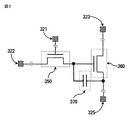
- FIG. 3 is a circuit diagram of a pixel driving circuit in the first embodiment of the present invention.
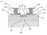
- FIG. 4 is a view showing a cross-sectional structure of an organic TFT in the first embodiment of the present invention.
- FIG. 5 is a diagram showing a cross-sectional structure of an organic TFT of a pixel drive circuit substrate in the second embodiment of the present invention.
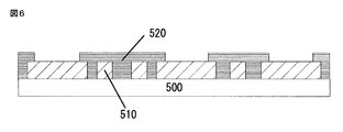
- FIG. 6 is a diagram showing a cross-sectional structure of a third substrate in the second embodiment of the present invention.
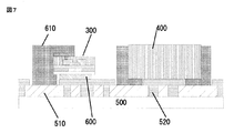
- FIG. 7 is a cross-sectional view in which the pixel drive circuit substrate 300 and the inorganic LED element 400 are mounted on a third substrate according to the second embodiment of the present invention.
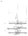
- FIG. 8 is a diagram showing an example of a bonding method for realizing a large display by bonding a third substrate in the second embodiment of the present invention.
- FIG. 1 shows the basic concept of the present invention.
- a pixel driving circuit board 300 is provided for each of three color elements in each pixel of a substrate 100 of a display body, and inorganic LEDs 410, 411, 412 for surface mounting of RGB colors. Is shown.
- 232, 233, and 234 are formed, and further, a wiring pattern 235 for connecting the output terminal 325 of the pixel drive circuit board and the anode of the LED is formed.
- Terminals 321, 322, 323, and 325 connected to an internal circuit are provided on the pixel driving circuit board, and each is mounted face down so as to connect to the pads 231, 232, and 233 and the wiring pattern 235. .
- Each LED is mounted so that the anode is connected to 235 and the cathode is connected to 234.
- FIG. 2 shows a state of the pixel driving circuit substrate 300 and the substrate 100 before mounting the LEDs.
- Printing technology represented by gravure offset printing and screen printing on the substrate 100 of the display body using resin base materials such as PET (polyethylene terephthalate), PEN (polyethylene naphthalate) and PI (polyimide).
- the pads 231, 232, 233, and 234 are connected to the row selection line, the column selection line, the power supply line, and the ground line via VIA, respectively.
- the row selection line 211 is laid out so as to be parallel to the long side of the display, and the column selection line 212 and the power supply line 213 are parallel to the row selection line 211 so as to be orthogonal to the row selection line 211 with the insulating film 110 interposed therebetween.
- the ground line 214 is laid out.
- the pads 231, 232, 233 and 234 and the wiring pattern 235 are formed on the insulating film 120.
- a pixel driving circuit a circuit composed of a selection TFT, a driving TFT, and a holding capacitor shown in FIG. 3 is taken as an example, but other circuit methods are selected as the scope of application of this patent. It doesn't matter.
- the pixel driving circuit can be formed by a high-performance organic TFT circuit process described in Non-Patent Document 1.
- FIG. 4 shows a cross-sectional portion of the organic transistor in the pixel drive circuit substrate 300.
- a pixel driving circuit substrate 300 using a resin base material represented by PEN or PI as a substrate material is bonded to a glass support substrate 301, and an organic TFT circuit process is performed.
- the main processes are the formation of the gate electrode 310, the formation of the gate insulating film 311, the formation of the organic semiconductor single crystal film 312, the formation of the metal film for the source electrode 313 and the drain electrode 314, the organic semiconductor single crystal film and the source electrode, It consists of patterning of the drain electrode, formation of the wiring layer 315, formation of the insulating film layer 316, formation of the VIA 317 and formation of the connection terminal pad 318.
- the pixel driving circuit is formed by laying out a large number of pixel driving circuits at a high density on a substrate having the most economical efficiency as an organic TFT process.
- the pixel driving circuit substrate 300 is peeled off from the support substrate 301 and mounted on the display substrate 100 in units of circuits.
- the holding capacitor element in the pixel driving circuit uses the gate insulating film 311 as a dielectric film and the metal films for the gate electrode 310, the source electrode 313, and the drain electrode 314 as electrodes. .
- a second embodiment for carrying out the present invention will be described.
- a pixel driving circuit composed of an organic semiconductor thin film is formed on a first substrate, and a second is performed by an inorganic semiconductor process.
- An inorganic LED element is formed on the substrate, a wiring or a terminal pattern is formed on the third substrate by various printing methods or photolithography methods, and the first substrate and a predetermined portion on the third substrate are formed.
- An active matrix LED display is manufactured by bonding and mounting the second substrate. The difference from the first embodiment is that it is mounted face up with respect to face down.
- a pixel driving circuit substrate 300 FIG.
- FIG. 5 formed of a thin film transistor having a two-transistor one-capacitor (2Tr1C) structure shown in FIG. 3 is formed on a first substrate.
- 2Tr1C two-transistor one-capacitor
- the configuration of the first substrate is such that a resin substrate 300 having flexibility is formed on a temporary fixing substrate 301 for handling in the process.
- the temporarily fixed substrate for handling is not particularly limited as long as it is a rigid substrate having good dimensional stability, such as non-alkali glass, quartz glass, and Si substrate.
- the resin substrate having flexibility for example, polyethylene terephthalate (PET), polyethylene naphthalate (PEN), polycarbonate (PC), polyimide (PI), polyethersulfone (PES), polyetherimide ( PEI), polyphenylene sulfide (PPS), wholly aromatic polyamide (also known as aramid), polyphenylene ether (PPE), polyarylate (PAR), polybutylene terephthalate (PBT), polyoxymethylene (POM, also known as polyacetal), poly Examples include ether ether ketone (PEEK), liquid crystal polymer (LCP) (eg, molten liquid crystalline wholly aromatic polyester (basic skeleton: parahydroxybenzoic acid, biphenol, phthalic acid)), parylene, metal foil substrate, and the like.
- PET polyethylene terephthalate
- PEN polyethylene naphthalate
- PC polycarbonate
- PI polyimide
- PES polyethersulfone
- PEI polyetherimide
- the film thickness of the resin substrate is 1 ⁇ m to 500 ⁇ m and can be freely set according to the purpose, more preferably 1 ⁇ m to 150 ⁇ m, and most preferably 1 ⁇ m to 50 ⁇ m.
- the conductive thin film 310 is formed on the resin substrate.
- the conductive thin film 310 is formed on the resin substrate 300 by a sputtering method, a PVD method typified by a vacuum deposition method, or a coating method using an ink containing a conductive film material.
- An example is a method of forming a film by forming a film on the surface and then patterning the film into a predetermined shape by a photolithography method.
- Examples of the material for forming the conductive thin film 310 include metals such as Au, Ag, Cu, Mo, W, Ti, Al, Pd, Pt, and Ta, alloys of these metals, and compounds of these metals. Can be mentioned. As a material for forming the conductive film, a material having high conductivity is preferable. As another method for forming the conductive thin film 310, for example, the conductive thin film 310 patterned in a predetermined shape is directly formed on the resin substrate 510 by a plate printing method or a plateless printing method. A method is mentioned. By directly forming the conductive thin film 310 patterned into a predetermined shape, the process of forming the conductive thin film 310 can be simplified.
- inks containing various conductive film materials can be used.
- an ink containing a highly conductive material is preferable.
- an ink containing a conductive polymer compound such as PEDOT / PSS, a fine particle dispersed ink in which nanoparticle fine particles of an inorganic material are dispersed.
- metal compound inks such as copper salts and silver salts.
- the fine particles contained in the fine particle dispersed ink include nano-Au, nano-Ag, nano-Cu, nano-Pd, nano-Pt, nano-Ni, nano-ITO, nano-silver oxide, and nano-copper oxide. Can be mentioned.
- the fine particle dispersed ink containing nano-silver oxide and nano-copper oxide may contain a reducing agent.
- the conductive thin film 310 may be formed by a plating method. As a method of forming the conductive thin film 310 by a plating method, for example, a plating primer layer patterned in advance into a predetermined shape is formed on the resin substrate 300 by a photolithography method, a plate printing method or a plateless printing method.
- a method of forming the conductive thin film 310 at a predetermined position by an electroless plating method or a combination of an electroless plating method and an electrolytic plating method may be used.
- the thickness of the conductive thin film 310 is not particularly limited, but is preferably 20 nm to 1 ⁇ m, and more preferably 20 nm to 300 nm.
- the thickness of the conductive thin film 310 is preferably 100 nm to 300 nm, and preferably 150 nm to 250 nm. More preferred.
- the nanoparticle fine particles contained in the conductive thin film 310 become non-uniform due to particle growth. This is because there is a possibility that the conductivity may be hindered, and the conductivity may be lowered at a film thickness of 100 nm or less.
- the film thickness is preferably 20 nm to 100 nm, and more preferably 20 nm to 60 nm.
- a gate insulating film 311 is formed on the resin substrate 300 and the conductive thin film 310.
- the gate insulating film 311 is preferably an organic insulating film containing a ferroelectric or high molecular compound having a high relative dielectric constant.
- the ferroelectric having a high relative dielectric constant include inorganic metal compounds typified by alumina (AlxOy) and hafnium oxide (HfxOy).
- the polymer compound examples include PS resin, PVP resin, PMMA resin, fluorine-containing resin, PI (polyimide) resin, PC (polycarbonate) resin, PVA (polyvinyl alcohol) resin, parylene resin, and these resins.
- examples thereof include a copolymer containing a plurality of repeating units.
- a crosslinkable polymer compound is preferable because of excellent process resistance and stability typified by solvent resistance.
- the thickness of the gate insulating film 311 is not particularly limited, but is preferably 1 nm to 1 ⁇ m, more preferably 20 nm to 100 nm, and still more preferably 30 nm to 80 nm.
- a more preferable structure for forming the gate insulating film 311 is more preferably a laminated film of a ferroelectric and an organic insulating film.
- Alumina / PS resin, alumina / PVP resin, alumina / PMMA resin, alumina / fluorine resin, alumina / polyimide The structure represented by resin, an alumina / PVA resin, an alumina / parylene resin etc. can be considered.
- each structure is preferably 10 nm to 500 nm for the ferroelectric, 10 nm to 500 nm for the organic insulating film, more preferably 10 nm to 50 nm for the ferroelectric, and 10 nm to 100 nm for the organic insulating film, More preferably, the ferroelectric is 10 nm to 40 nm, and the organic insulating film is 10 nm to 40 nm.
- an organic semiconductor thin film 312 is formed over the gate insulating film 311. Examples of the method for forming the organic semiconductor thin film 312 include a method of selectively forming a material for forming the organic semiconductor thin film 312 only in a predetermined region where the organic semiconductor thin film 312 is to be formed.
- the organic semiconductor thin film 312 is formed only in a predetermined region by forming a material for forming the organic semiconductor thin film 312 by a PVD method typified by a vacuum deposition method through a mask typified by a metal mask or the like. Form. Furthermore, a resin film having an opening may be formed only in a predetermined region where the organic semiconductor thin film 312 is to be formed, and then the organic semiconductor thin film 312 may be formed on one surface by a vacuum deposition method. In this case, it is preferable that the opening of the resin film is formed in an inversely tapered shape in which the opening area decreases as the distance from the substrate 1 increases.
- the organic semiconductor thin film 312 formed in the opening and the organic semiconductor thin film 312 formed on the resin film are cut, and the resin This is because the membrane functions suitably as a separator.
- the organic semiconductor thin film 312 is formed into a gate insulating film 311 by a PVD method typified by a vacuum deposition method or a coating method using an ink containing an organic semiconductor material.
- a PVD method typified by a vacuum deposition method or a coating method using an ink containing an organic semiconductor material.
- An example is a method of forming a film by forming a film on the surface and then patterning the film into a predetermined shape by a photolithography method.
- the organic semiconductor thin film 312 patterned in a predetermined shape is directly formed on the gate insulating film 311 by, for example, plate printing or plateless printing.
- a method is mentioned.
- the process of forming the organic semiconductor thin film 312 can be simplified.
- an organic material oriented in a uniaxial direction on the entire surface of the gate insulating film 311 by a coating method using a plateless printing method since a high current capability is required to drive the inorganic LED element, among these, an organic material oriented in a uniaxial direction on the entire surface of the gate insulating film 311 by a coating method using a plateless printing method.
- a method of forming a single crystal film and obtaining an organic semiconductor thin film 312 patterned into a predetermined shape by photolithography is most preferable.
- An organic single crystal film oriented in a uniaxial direction is formed on the entire surface of the gate insulating film 311 by a coating method using a plateless printing method, and then an organic semiconductor thin film 312 patterned into a predetermined shape by a photolithography method is formed.
- ink containing various organic semiconductor materials can be used, but it is preferable to use ink containing a low molecular organic semiconductor material.
- a baking treatment may be performed in order to control the morphology of the organic semiconductor thin film 312 or to volatilize the solvent contained in the organic semiconductor thin film 312.
- the thickness of the organic semiconductor thin film 312 is not particularly limited, but is preferably 1 nm to 1000 nm, more preferably 1 nm to 100 nm, and still more preferably 1 nm to 50 nm. More preferably, the best film is not a film thickness but a crystal film having 3 to 5 molecular layers or less.
- organic semiconductor materials include low molecular compounds that can be formed by vapor deposition, such as pentacene and copper phthalocyanine.
- Examples of compounds that can be formed by coating include 6,13-bis (triisopropylsilyl). Ethynyl) pentacene (6,13-bis (triisopropylsilyltyny) pentacene (Tips-Pentacene)), 13,6-N-sulfinylacetamidopentacene (13,6-N-sulfinylacetamidopentenecene (NSFAAP)), 6,13-hydro 13-methanopentacene-15-one (6,13-Dihydro-6,13-methanepentenecene-15-one (DMP)), pentacene-N- Rufinyl-n-butylcarbamate adduct (typified by Pentacene-N-sulfinyl-tert-butylcarbamate), pentacene-N-sulfinyl-tert-butylcarbamate, and the like Precursor, [1
- a patterned conductive thin film 315 is formed on the gate insulating film 311 and the organic semiconductor thin film 312. With the conductive thin film 315, the source electrode and the drain electrode of the organic thin film transistor are formed.
- the conductive thin film 315 can be formed by a method similar to that of the conductive thin film 310 described above. Note that the conductive thin film 315 may be formed by the same method as the conductive thin film 310 or by a different method.
- the film thickness of the conductive thin film 315 (that is, the film thickness of the source electrode and the drain electrode of the organic thin film transistor) is not particularly limited, but is preferably 20 nm to 1 ⁇ m, more preferably 20 nm to 600 nm, and more preferably 20 nm to 500 nm. More preferably.
- a protective film 316 is formed over the gate insulating film 311, the organic semiconductor thin film 312, and the conductive thin film 315.
- a method for forming the protective film 316 for example, a PVD method typified by a vacuum deposition method, a CVD method typified by an ALD (atomic layer deposition) method, or a coating method using an ink containing a protective layer material is used.
- An example is a method of forming 316 by patterning into a predetermined shape by a photolithography method.
- a method of directly forming the protective film 316 patterned into a predetermined shape by a plate printing method or a plateless printing method can be mentioned.
- the process of forming the protective layer 316 can be simplified.
- a method of directly forming the protective layer 316 patterned into a predetermined shape by a plate printing method or a plateless printing method is preferable.
- inks containing various protective layer materials can be used.
- the ink containing the protective layer material include a dispersion ink containing an inorganic material, an SOG (spin on glass) material, an ink containing a low molecular protective layer material, and an ink containing a polymer protective layer material. Inks containing layer material are preferred.
- the material for forming the protective film 316 include the same materials as those exemplified in the above-described gate insulating film 311 in addition to the materials contained in the ink and the SOG material.
- the thickness of the protective film 316 is not particularly limited, but is preferably 50 nm to 5 ⁇ m, and more preferably 500 nm to 3.0 ⁇ m.
- an upper electrode 318 is formed on the protective layer 316, whereby the first substrate on which the pixel driving circuit is formed is completed.
- a method for forming the upper electrode 318 is not particularly limited, and examples thereof include a photolithography method, a plate printing method, and a plateless printing method. Among them, a screen (stencil) printing method which is one of the plate printing methods is used. The method is preferred.
- the inorganic LED element 400, which is the second substrate may be commercially available or purchased directly from the manufacturer as a component and mounted on the third substrate using a chip mounter.
- the more preferable inorganic LED element is the bare chip LED element, and the size is preferably 0.25 ⁇ 0.27 mm to 0.4 ⁇ 0.2 mm (so-called 0201 to 0402).
- an inorganic LED element having a size of 1.6 ⁇ 1.5 mm (1615) mixed with three colors in one chip may be used for a single color light emission, and 1.6 ⁇ 0.8 mm (1608). I do not care.
- the most preferred form is a full-color bare chip inorganic LED element.
- a third substrate (FIG. 6) is manufactured.
- the third substrate may be fixed to the carrier substrate in the same manner as the first substrate, or the process may be performed by roll-to-roll, and an optimum method at that time can be used.
- an electrode pattern 510 is formed on a third substrate.
- a screen printing method is most preferable, but patterning may be performed using a photolithography method.
- an electrode pattern 510 is obtained by appropriately performing a baking process or the like.
- an insulating film pattern 520 having an opening at a position where the terminal portion at the end of the substrate, the pixel driving circuit substrate 300 and the inorganic LED element 400 are mounted is formed thereon.
- a screen printing method is most preferable.
- the insulating film pattern 520 may be patterned by slit coating or spin coating and photolithography.
- the insulating film pattern 520 is obtained by appropriately performing a baking process or the like.
- the third substrate is completed.
- the pixel drive circuit substrate 300 and the inorganic LED element 400 are mounted on the third substrate on the third substrate (FIG. 7).
- mounting may be performed using a general chip mounter device.
- the adhesive 600 may be formed in a pattern by a screen printing method or the like at a position where it is mounted in advance.
- the mounting component may be fixed by applying an Ag paste 610 before sintering to a place where the pixel driving circuit board 300 and the inorganic LED element 400 are mounted by screen printing before and after mounting, and sintering after mounting.
- the best mounting method is that the adhesive 600 is applied in advance to the mounting portion of the pixel driving circuit board 300, the pixel driving circuit board 300 is mounted and fixed on the face-up, and then the Ag paste 610 is applied to the screen. Printing is performed so as to straddle the terminal portion of the pixel drive circuit board 300 and the connection terminal for connecting to the pixel drive circuit board 300 provided on the third substrate, and the inorganic LED element 400 is mounted in the same process.
- a pattern of Ag paste 610 is also formed on the connection terminal portion for this purpose.
- the size of the third board may be basically set in accordance with the work size of the printed circuit board, and it is necessary to incorporate special specifications when introducing a manufacturing apparatus such as a screen printer. Disappears.
- the maximum size of a copper-clad laminate is determined to be 1000 (1020) ⁇ 1000 (1020) mm or 1000 (1020) ⁇ 1200 (1220) mm, and this is divided into four to be 500 (510) ⁇ 500 (510 ) It can be used as a work size of mm ⁇ or smaller.
- a large active matrix LED display can be realized by laminating a plurality of 500 ⁇ 500 mm square substrates in the column direction or the row direction.
- the bonding surface 700 connecting the third substrates is at least an electrode terminal. It is preferable that the part is bonded using a conductive adhesive 710 and the other substrate parts are connected by a resin adhesive 720 (FIG. 8A). Alternatively, it is most preferable that there is a bonding mechanism 740 using a magnet 730 or the like at each panel end, and the substrates are connected with one touch (FIG. 8B).
- a pixel driving circuit using a high-performance organic TFT capable of driving an LED and an inorganic LED element, which are independently manufactured on a substrate different from the display substrate, are mounted on the display substrate.
- a pixel driving circuit using organic TFTs may be formed directly on the display substrate, and an inorganic LED element may be mounted thereon.
- the circuit and wiring necessary for controlling the inorganic LED pixels are minimized, the entire display can be reduced in weight, the installation cost can be reduced, and the large LED display substrate can be made super flexible.
Landscapes
- Engineering & Computer Science (AREA)
- Physics & Mathematics (AREA)
- General Physics & Mathematics (AREA)
- Theoretical Computer Science (AREA)
- Manufacturing & Machinery (AREA)
- Devices For Indicating Variable Information By Combining Individual Elements (AREA)
- Electroluminescent Light Sources (AREA)
- Microelectronics & Electronic Packaging (AREA)
- Led Device Packages (AREA)
Abstract
Description
フラットパネルディスプレイの新しい分野として、交通機関や小売店等で紙に代わる広告媒体としてディスプレイを使用するデジタルサイネージ市場の拡大が期待されている。現在は、小型のディスプレイによる電車内での広告や情報発信、小売店でのPOP広告的な使われ方が主流だが、大型ディスプレイにデジタルサイネージに対する潜在的なニーズが高い。大型商業施設や繁華街或はイベント会場にて、ロケーションや消費者の行動状況に応じた映像系広告や販促情報さらにはイベント・サービスの案内等を大型のディスプレイを用いて発信することにより消費行動を促進することが検討されている。大型ディスプレイによる広告効果の高さは実証実験等でも確認されている。
ところが、市場の期待の大きさにかかわらず、デジタルサイネージにおけるディスプレイの大型化の進展は緩やかである。現状のディスプレイ技術ではコスト及び機能面において課題があり、普及し得る大型ディスプレイ技術が存在しない点にある。コストに関しては、ディスプレイ本体のコストに加えて大型であるが故の設置コストの抑制も重要な要素になる。また、大型ディスプレイを設置する箇所の殆どは既存の構造物の内外部であるため、既存の構造物に対する加工が極力少なく、スペースを有効に活用できるディスプレイ技術が求められる。言い換えると、軽量で曲げることが可能で且つ任意の形状に低コストで製造できる大型ディスプレイ技術が求められている。
しかしながら、既存のフラットパネルディスプレイの主流である液晶ディスプレイ技術では、大きなガラス基板上にディスプレイを製造する性格上、大型化に伴い製造コストが急激に上昇する上、製造可能なサイズに上限が存在する。サイネージ向け等で40~50インチ程度の液晶ディスプレイを複数組み合わせることで大型化させる事例もあるが、ディスプレイ全体の重量増や屋外等への設置性が乏しいことなどから広く普及するに至っていない。
また、有機EL技術は軽量でフレキシブルなディスプレイを作ることに一番適しており、既に曲げることができるディスプレイが普及しているが、大型化の普及にはまだ量産技術の課題も多く、更に、サイネージ向けに使用するには、要求される輝度・寿命特性の実現に更なる特性の向上が必要である。
一方、LEDを用いたディスプレイは画素を適度なサイズでまとめたディスプレイユニットを組み合わせる方式で大型化するため、サイズ上の制限が原理的にはない。そのため、屋外等で使用する超大型のディスプレイにはLEDディスプレイが採用されている。しかし、現状の技術では画素を効率よく制御することが可能なアクティブマトリクス方式のディスプレイを作ることができないため、LED素子を実装する基板側に複雑な配線を施し、複雑な制御回路装置でディスプレイユニットの画像を制御する必要がある。そのため、ディスプレイのコストと重量抑制が困難であり、普及の足枷となっている。
本発明のアクティブマトリクスLEDディスプレイは、複数枚の基板を列方向と行方向に並べる事により大型化しており、列方向と行方向に並べられた複数枚の基板は、それぞれ独立した駆動回路を有しているもしくは、列方向と行方向に並べられた複数枚の基板は電気的に接続されており、全ての基板は共通の駆動回路を有している。
本発明のアクティブマトリクスLEDディスプレイの無機LED素子を実装するための画素駆動回路を備えた基板は、基板端に基板間接続端子を有し、更に基板上に行選択線、列選択線、電源線とグランド線を有し、かつ、ディスプレイの画素を構成する単位毎に少なくとも、片側が電源線もしくはグランド線に接続された無機LED素子実装用端子を有している。
本発明のアクティブマトリクスLEDディスプレイは、画素駆動回路が形成された画素駆動回路基板、無機LED素子とこれらを実装するためのパターンを備えた第3の基板の3部材を組み合わせて構成されており、画素駆動回路基板と第3の基板は可撓性を有している。
本発明のアクティブマトリクスLEDディスプレイの画素駆動回路基板は、少なくとも行選択線接続用端子、列選択線接続用端子、電源線接続用端子、無機LED接続用端子の4端子を有している。
本発明のアクティブマトリクスLEDディスプレイの画素駆動回路基板と無機LED素子を実装するための第3の基板は、基板端に基板間接続端子を有し、更に基板上に行選択線、列選択線、電源線とグランド線を有し、かつ、ディスプレイの画素を構成する単位毎に少なくとも行選択線接続用端子、列選択線接続用端子、電源線もしくはグランド線接続用端子、片側が電源線もしくはグランド線に接続された無機LED素子実装用端子を有している。
本発明のアクティブマトリクスLEDディスプレイは、無機LED素子を実装するための画素駆動回路を備えた基板および、画素駆動回路が形成された画素駆動回路基板、無機LED素子とこれらを実装するためのパターンを備えた第3の基板で構成されており、基板端部に基板同士を貼り合せるもしくは、電気的に接合するための接合機構を備えている。
本発明のアクティブマトリクスLEDディスプレイは、無機LED素子を画素駆動回路が備えられた基板上に部品として実装工程で貼り合わされている。
本発明のアクティブマトリクスLEDディスプレイは、画素駆動回路を備えた可撓性を有する画素駆動回路基板、無機LED素子とこれらを実装するためのパターンを備えた可撓性を有する第3の基板の3部材を組み合わせて構成されており、画素駆動回路基板と無機LED素子は第3の基板上に実装工程で貼り合せる。
本発明のアクティブマトリクスLEDディスプレイを列方向と行方向に複数並べて大型化するとき、隣接するアクティブマトリクスLEDディスプレイとは少なくとも一部に導電性を備えた材料を含む部材もしくは、接合機構を用いて貼り合せている。
具体的には、有機LED(有機EL,OLED)素子と違い、無機LED素子は既存の固体半導体プロセスで形成し高温な熱処理が施される部材を無機LED素子に限定できるため、これを部品として基材上に実装する場合にはプロセス制約がなく、ディスプレイ基板として安価なポリエチレンテレフタレート(PET)などのフレキシブル基板が利用できる。これにより、ディスプレイ基板上の表示エリア全面に張りめぐらせる各種配線類や絶縁膜は安価なロールツーロール技術や印刷技術等で形成することが可能になり、さらに画素駆動回路は有機TFTプロセスにとって最も経済効率の高いサイズのフレキシブル基板上に高密度に形成することが可能になる。このことにより、ディスプレイ全体の大型化に伴う製造コストの増大は最小限に抑制できる。加えて、軽量で且つフレキシブルな大型アクティブマトリクスLEDディスプレイが実現できる。
図2は本発明の第1の実施形態において、LEDと画素駆動回路基板300を実装する直前のディスプレイ基板100の状態を示した図。図ではディスプレイ基板100の上面の一部を拡大した上面図と、上面図に破線で示した箇所の断面図を示している。上面図中の一点鎖線は各画素の境界を表している。
図3は本発明の第1の実施形態における、画素駆動回路の回路図。
図4は本発明の第1の実施形態における、有機TFTの断面構造を示した図。
図5は本発明第2の実施形態における、画素駆動回路基板の有機TFTの断面構造を示した図。
図6は本発明第2の実施形態における、第3の基板の断面構造を示した図。
図7は本発明第2の実施形態における、第3の基板へ画素駆動回路基板300と無機LED素子400を実装した断面図。
図8は本発明第2の実施形態における、第3の基板を貼り合せて大型ディスプレイを実現するための接合方法の例を示す図面
図1は本発明の基本概念を示すものであり、ディスプレイ本体の基板100の各画素内の3つの色要素毎に画素駆動回路基板300及び、RGB各色の表面実装用の無機LED410,411,412を実装する様子を示している。ディスプレイ基板100上には、画素駆動回路基板と無機LEDを実装する段階で、行選択線、列選択線、電源線、グランド線とこれらの導体線の各々と電気的に接続されているパッド231、232、233、234が形成されており、さらに画素駆動回路基板の出力端子325とLEDの陽極を接続するための配線パターン235が形成されている。画素駆動回路基板上には内部回路に接続される端子321、322、323、325が設けられており夫々が、バッド231、232、233及び配線パターン235に接続するようにフェイスダウンにより実装される。各LEDは陽極が235、陰極が234に接続するように実装される。
本実施の形態では、アクティブマトリクス動作させるために必要な導体線の全てを画素駆動回路基板及びLEDを実装する前に形成しているが、この一部の形成工程が、画素駆動回路基板やLEDの実装工程と前後しても本発明の適用範囲として構わない。
図2に画素駆動回路基板300及びLEDを実装する前の基板100の状態を示す。PET(ポリエチレンテレフタレート)、PEN(ポリエチレンナフタレート)、PI(ポリイミド)に代表される樹脂基材を材料としたディスプレイ本体の基板100に対して、グラビアオフセット印刷やスクリーン印刷に代表される印刷技術を用いて、行選択線211、列選択線212、電源線213、グランド線214を、さらにこれらの導体線とLED及び画素駆動回路を電気的に接続するためのバッド231、232、233、234と、LEDと駆動回路の出力を接続するための配線パターン235を形成する。図では省力しているが、バッド231、232、233、234は夫々行選択線、列選択線、電源線、グランド線にVIAを介して接続されている。行選択線211はディスプレイの長辺に平行なるようにレイアウトされ、絶縁膜110を挟んで行選択線211と直行するように列選択線212と電源線213が、行選択線211と平行するようにグランド線214がレイアウトされている。パッド231、232、233、234及び配線パターン235は絶縁膜120の上に形成する。
本実施の形態では、画素駆動回路としては図3に示す選択用TFTと駆動用TFT及び保持用容量素子で構成する回路を例としてあげるが、本特許の適用範囲としては他の回路方式を選んでも構わない。
画素駆動回路は非特許文献1等の高性能有機TFT回路プロセスにより形成することができる。図4に画素駆動回路基板300内の有機トランジスタの断面部を示す。ガラスの支持基板301にPENやPI等に代表される樹脂基材を基板材とする画素駆動回路基板300を張り合わせて、有機TFT回路プロセス処理を行う。主だった工程は、ゲート電極310の形成、ゲート絶縁膜311の形成、有機半導体単結晶膜312の形成、ソース電極313及びドレイン電極314用金属膜の形成、有機半導体単結晶膜とソース電極及びドレイン電極のパターニング、配線層315の形成、絶縁膜層316の形成、VIA317の形成と接続端子用パッド318の形成からなる。画素駆動回路は、有機TFTプロセスとして最も経済効率の高いサイズの基板に対して、多数の画素駆動回路を高密度にレイアウトして形成する。画素駆動回路の形成後に、回路単位で画素駆動回路基板300を支持基板301から剥離し、ディスプレイ基板100に実装する。
図4では明示的に示していないが、画素駆動回路における保持用容量素子は誘電体膜としてゲート絶縁膜311を、電極としてゲート電極310及びソース電極313やドレイン電極314用の金属膜を使用する。
本実施の形態は、本発明を実施するための第1の実施の形態で示したとおり、第1の基板上に有機半導体薄膜で構成された画素駆動回路を形成し、無機半導体プロセスにより第2の基板上に無機LED素子を形成し、第3の基板上に各種印刷法やフォトリソグラフィー法などで配線や端子パターンを形成し、第3の基板上の所定の箇所へ前記第1の基板と前記第2の基板を貼り合せて実装することでアクティブマトリクスLEDディスプレイを作製するものである。前記第1の実施の形態との違いは、フェイスダウンに対してフェイスアップで実装する点である。
次に、本発明を実施するための第2の実施の形態について詳細を説明する。
最初に、第1の基板上に図3に示す2トランジスタ1キャパシタ(2Tr1C)構成の薄膜トランジスタで形成された画素駆動回路基板300(図5)を形成する。但し、図5とそれ以降の図面では簡略化のため1トランジスタの簡略表示にて説明するが、実際には、図3に代表される回路を構成する要素が入っているものとする。
第1の基板の構成は、工程中のハンドリング用仮固定基板301上に可撓性を有する樹脂製基板300が形成されているものである。この時、ハンドリング用仮固定基板としては、無アルカリガラス、石英ガラス、Si基板等に代表される寸法安定性の良いリジットな基板なら特に制限されるものではない。
また、可撓性を有する樹脂製基板としては、例えば、ポリエチレンテレフタレート(PET)、ポリエチレンナフタレート(PEN)、ポリカーボネート(PC)、ポリイミド(PI)、ポリエーテルサルホン(PES)、ポリエーテルイミド(PEI)、ポリフェニレンサルファイド(PPS)、全芳香族ポリアミド(別名:アラミド)、ポリフェニレンエーテル(PPE)、ポリアリレート(PAR)、ポリブチレンテレフタレート(PBT)、ポリオキシメチレン(POM、別名:ポリアセタール)、ポリエーテルエーテルケトン(PEEK)、液晶ポリマー(LCP)(例:溶融液晶性全芳香族ポリエステル(基本骨格:パラヒドロキシ安息香酸、ビフェノール、フタル酸))、パリレン、金属ホイル基板等が挙げられる。
また、樹脂製基板の膜厚は1μm~500μmで目的に応じて自由に設定でき、より好ましくは1μm~150μm、最も好ましいのは1μm~50μmである。
次に、樹脂基板上に導電性薄膜310を形成する。導電性薄膜310を形成する方法としては、例えば、スパッタリング法、真空蒸着法に代表されるPVD法、または、導電性膜材料を含むインクを用いた塗布法により導電性薄膜310を樹脂製基板300上に成膜した後、フォトリソグラフィー法により所定の形状にパターニングを実施することにより形成する方法が挙げられる。
導電性薄膜310を形成する材料としては、例えば、Au、Ag、Cu、Mo、W、Ti、Al、Pd、Pt、Ta等の金属、これらの金属の合金、および、これらの金属の化合物が挙げられる。導電性膜を形成する材料としては、導電性が高い材料が好ましい。
また、導電性薄膜310を形成する他の方法としては、例えば、有版印刷法または無版印刷法により、樹脂製基板510上に、所定の形状にパターニングされた導電性薄膜310を直接形成する方法が挙げられる。所定の形状にパターニングされた導電性薄膜310を直接形成することにより、導電性薄膜310を形成する工程を簡略化することができる。
有版印刷法または無版印刷法により、所定の形状にパターニングされた導電性薄膜310を直接形成する場合、種々の導電性膜材料を含むインクを用いることができる。導電性膜材料を含むインクとしては、導電性の高い材料を含むインクが好ましく、例えば、PEDOT/PSS等の導電性高分子化合物を含むインク、無機材料のナノパーティクル微粒子を分散させた微粒子分散インク、銅塩、銀塩等の金属化合物インクが挙げられる。微粒子分散インクに含まれる微粒子としては、例えば、ナノ−Au、ナノ−Ag、ナノ−Cu、ナノ−Pd、ナノ−Pt、ナノ−Ni、ナノ−ITO、ナノ−酸化銀、ナノ−酸化銅が挙げられる。ナノ−酸化銀およびナノ−酸化銅を含む微粒子分散インクには、還元剤が含まれていてもよい。
また、めっき法により導電性薄膜310を形成してもよい。めっき法により導電性薄膜310を形成する方法としては、例えば、フォトリソグラフィー法、有版印刷法または無版印刷法により、あらかじめ所定の形状にパターニングされためっきプライマー層を樹脂製基板300上に形成しておき、無電解めっき法、または、無電解めっき法と電解めっき法との組合せにより、所定の位置に導電性薄膜310を形成する方法が挙げられる。
導電性薄膜310の膜厚は特に限定されないが、20nm~1μmであることが好ましく、20nm~300nmであることがより好ましい。無機材料のナノパーティクル微粒子を分散させた微粒子分散インクを用いて導電性薄膜310を形成する場合、導電性薄膜310の膜厚は、100nm~300nmであることが好ましく、150nm~250nmであることがより好ましい。微粒子分散インクに含まれる分散剤成分等の残留や導電性薄膜310の成膜後のベーク処理において、ナノパーティクル微粒子が粒子成長することで導電性薄膜310に含まれるナノパーティクル微粒子が不均一となることにより導電性の阻害が発生する可能性があるため、100nm以下の膜厚では導電性が低下する可能性があるためである。
一方、銀塩等を用いて導電性薄膜310を形成する場合は、膜厚は20nm~100nmが好ましく、20nm~60nmがより好ましい。これは、銀塩などではナノパーティクル微粒子の成長よりも緻密な膜が形成されより薄い膜厚でも導電性が発現するからである。更に薄くできることで、ゲート電極の段差が低くなりその上の絶縁膜の信頼性向上にも寄与できる。
次に、樹脂製基板300および導電性薄膜310の上に、ゲート絶縁膜311を形成する。ゲート絶縁膜311としては、高い比誘電率を有する強誘電体や高分子化合物を含有する有機絶縁膜が好ましい。高い比誘電率を有する強誘電体としては、アルミナ(AlxOy)、酸化ハフニウム(HfxOy)に代表される無機の金属化合物があげられる。高分子化合物としては、例えば、PS樹脂、PVP樹脂、PMMA樹脂、含フッ素樹脂、PI(ポリイミド)樹脂、PC(ポリカーボネート)樹脂、PVA(ポリビニルアルコール)樹脂、パリレン樹脂および、これらの樹脂に含まれる繰り返し単位を複数含む共重合体が挙げられる。これらの中でも、高分子化合物としては、耐溶剤性に代表されるプロセス耐性および安定性に優れるため、架橋性の高分子化合物が好ましい。
ゲート絶縁膜311の膜厚は特に限定されないが、1nm~1μmであることが好ましく、20nm~100nmであることがより好ましく、30nm~80nmであることが更に好ましい。
ゲート絶縁膜311を形成するより好ましい構造は、強誘電体と有機絶縁膜の積層膜がより好ましく、アルミナ/PS樹脂、アルミナ/PVP樹脂、アルミナ/PMMA樹脂、アルミナ/含フッ素樹脂、アルミナ/ポリイミド樹脂、アルミナ/PVA樹脂、アルミナ/パリレン樹脂などに代表される構造が考えられる。各構造の膜厚は、強誘電体が10nm~500nm、有機絶縁膜が10nm~500nmであるのが好ましく、強誘電体が10nm~50nm、有機絶縁膜が10nm~100nmであるのがより好ましく、強誘電体が10nm~40nm、有機絶縁膜が10nm~40nmであるのが更に好ましい。
次にゲート絶縁膜311上に有機半導体薄膜312を形成する。有機半導体薄膜312を形成する方法としては、例えば、有機半導体薄膜312が形成されるべき所定の領域にのみ、選択的に有機半導体薄膜312を形成する材料を成膜する方法が挙げられる。
具体的には、メタルマスク等に代表されるマスクを介して、真空蒸着法に代表されるPVD法により有機半導体薄膜312を形成する材料を所定の領域にのみ成膜することによって有機半導体薄膜312を形成する。
さらには、有機半導体薄膜312が形成されるべき所定の領域のみ、開口部を有する樹脂膜を形成し、その後、有機半導体薄膜312を真空蒸着法で一面に形成してもよい。この場合、樹脂膜の開口部は、基板1から離間するほどその開口面積が小さくなる逆テーパー形状に形成されていることが好ましい。逆テーパー形状に形成された開口部を有する樹脂膜を用いることにより、開口部内に形成された有機半導体薄膜312と樹脂膜上に形成された有機半導体薄膜312とが切断されることになり、樹脂膜がセパレーターとして好適に機能するためである。
また、有機半導体薄膜312を形成する他の方法としては、例えば、真空蒸着法に代表されるPVD法、または、有機半導体材料を含むインクを用いた塗布法により有機半導体薄膜312をゲート絶縁膜311上に成膜した後、フォトリソグラフィー法により所定の形状にパターニングを実施することにより形成する方法が挙げられる。
更に、有機半導体薄膜312を形成する他の方法としては、例えば、有版印刷法または無版印刷法により、ゲート絶縁膜311上に、所定の形状にパターニングされた有機半導体薄膜312を直接形成する方法が挙げられる。所定の形状にパターニングされた有機半導体薄膜312を直接形成することにより、有機半導体薄膜312を形成する工程を簡略化することができる。
但し、本発明では無機LED素子を駆動するために高い電流能力が求められるため、これらの中では、無版印刷法を用いた塗布法によりゲート絶縁膜311上全面に1軸方向に配向した有機単結晶膜を成膜し、フォトリソグラフィー法により所定の形状にパターニングされた有機半導体薄膜312を得る方法が最も好ましい。
無版印刷法を用いた塗布法によりゲート絶縁膜311上全面に1軸方向に配向した有機単結晶膜を成膜し、その後、フォトリソグラフィー法により所定の形状にパターニングされた有機半導体薄膜312を形成する場合、種々の有機半導体材料を含むインクを用いることができるが、低分子有機半導体材料を含むインクを用いることが好ましい。また、有機半導体薄膜312を成膜した後に、有機半導体薄膜312のモルフォロジーを制御するためや有機半導体薄膜312に含まれる溶媒を揮発させるために、焼成処理を実施してもよい。有機半導体薄膜312の膜厚は特に限定されないが、1nm~1000nmであることが好ましく、1nm~100nmであることがより好ましく、1nm~50nmであることが更に好ましい。最良な膜は、膜厚ではなく3~5分子層以下の結晶膜で有るのがより好ましい。
有機半導体材料としては、蒸着により成膜可能な低分子化合物として、例えば、ペンタセン(Pentacene)、銅フタロシアニンが挙げられ、塗布により成膜可能な化合物として、例えば、6,13−ビス(トリイソプロピルシリルエチニル)ペンタセン(6,13−bis(triisopropylsilylethynyl)pentacene(Tips−Pentacene))、13,6−N−スルフィニルアセトアミドペンタセン(13,6−N−sulfinylacetamidopentacene(NSFAAP))、6,13−ジヒドロ−6,13−メタノペンタセン−15−オン(6,13−Dihydro−6,13−methanopentacene−15−one(DMP))、ペンタセン−N−スルフィニル−n−ブチルカルバマート付加物(Pentacene−N−sulfinyl−n−butylcarbamate adduct)、ペンタセン−N−スルフィニル−tert−ブチルカルバマート(Pentacene−N−sulfinyl−tert−butylcarbamate)等に代表されるペンタセン前駆体、[1]ベンゾチエノ[3,2−b]ベンゾチオフェン([1]Benzothieno[3,2−b]benzothiophene(BTBT))、3,11−ジデシルジナフト[2,3−d:2’,3’−d’]ベンゾ[1,2−b:4,5−b’]ジチオフェン(3,11−didecyldinaphto[2,3−d:2’,3’−d’]benzo[1,2−b:4,5−b’]dithiophene(C10−DNBDT))、ベンゾビスチアジアゾール骨格を有するもの、ポルフィリン、ベンゾポルフィリン、可溶性基としてアルキル基等を有するオリゴチオフェン等に代表される低分子化合物またはオリゴマー、ポリチオフェン、フルオレンコポリマーやD−A構造を有するIDT−BT(indacenodithiophene benzothiadiazole)、CDT−BT(Cyclopentadithiophene benzothiadiazole)等に代表される高分子化合物が挙げられる。
次に、ゲート絶縁膜311および有機半導体薄膜312の上に、パターニングされた導電性薄膜315を形成する。この導電性薄膜315によって、有機薄膜トランジスタのソース電極およびドレイン電極が形成される。
導電性薄膜315は、前述の導電性薄膜310と同様の方法で形成することができる。なお、導電性薄膜315の形成は、導電性薄膜310の形成と同じ方法で形成しても異なる方法で形成してもよい。
導電性薄膜315の膜厚(すなわち、有機薄膜トランジスタのソース電極およびドレイン電極の膜厚)は特に限定されないが、20nm~1μmであることが好ましく、20nm~600nmであることがより好ましく、20nm~500nmであることが更に好ましい。
次に、ゲート絶縁膜311、有機半導体薄膜312と導電性薄膜315上に保護膜316を形成する。保護膜316を形成する方法としては、例えば、真空蒸着法に代表されるPVD法、ALD(atomic layer deposition)法に代表されるCVD法、保護層材料を含むインクを用いた塗布法により保護層316を成膜した後、フォトリソグラフィー法により所定の形状にパターニングを実施することにより形成する方法が挙げられる。また、保護層316を形成する他の方法としては、例えば、有版印刷法または無版印刷法により、所定の形状にパターニングされた保護膜316を直接形成する方法が挙げられる。所定の形状にパターニングされた保護層316を直接形成することにより、保護層316を形成する工程を簡略化することができる。
これらの中では、有版印刷法または無版印刷法により、所定の形状にパターニングされた保護層316を直接形成する方法が好ましい。
有版印刷法または無版印刷法により、所定の形状にパターニングされた保護層316を直接形成する場合、種々の保護層材料を含むインクを用いることができる。保護層材料を含むインクとしては、例えば、無機材料を含む分散インク、SOG(スピンオングラス)材料、低分子保護層材料を含むインク、高分子保護層材料を含むインクが挙げられるが、高分子保護層材料を含むインクが好ましい。
保護膜316を形成する材料としては、例えば、上記のインクに含まれる材料、SOG材料のほか、前述のゲート絶縁膜311において例示した材料と同様のものが挙げられる。
保護膜316の膜厚は特に限定されないが、50nm~5μmであることが好ましく、500nm~3.0μmであることがより好ましい。
最後に、保護層316上に上部電極318を形成することにより画素駆動回路が形成された第1の基板が完成する。上部電極318を形成する方法は特に限定されないが、例えば、フォトリソグラフィー法、有版印刷法および無版印刷法が挙げられ、中でも有版印刷法の一つであるスクリーン(孔版)印刷法を用いる方法が好ましい。
次に、第2の基板である無機LED素子400は、市販もしくは、直接メーカーから発光ダイオードを部品として購入しチップマウンタを用いて第3の基板に実装すればよい。より好ましい無機LED素子は、ベアチップのLED素子が最も好ましく、その大きさは、0.25×0.27mm~0.4×0.2mm(所謂、0201~0402)の大きさが好ましい。もしくは、単色発光なら1.6×0.8mm(1608)、フルカラーのものならば、1チップに3色混載されている1.6×1.5mm(1615)当たりの大きさの無機LED素子でも構わない。最も好ましい形は、フルカラー型のベアチップ無機LED素子である。
次に第3の基板(図6)を作製する。第3の基板は第1の基板と同様にキャリア基板に固定されていてもよいし、ロールtoロールでプロセスを実施しても良く、その時の最適な方法を用いることができる。
最初に、第3の基板上に電極パターン510を形成する。電極パターン510をパターン形成する方法としてはスクリーン印刷法が最も好ましいが、フォトリソグラフィー法を用いてパターニングしても良い。その後、適宜、焼成工程等を経る事で電極パターン510を得る。
次にその上に基板端の端子部、画素駆動回路基板300と無機LED素子400を実装する位置に開口がある絶縁膜パターン520をパターン形成する。絶縁膜パターン520をパターン形成する方法としてはスクリーン印刷法が最も好ましいが、スリットコート塗布やスピンコートで塗布を行い、フォトリソグラフィー法を用いてパターニングしても良い。この工程もまた、適宜、焼成工程等を経る事で絶縁膜パターン520を得る。この工程を経ることで、第3の基板が完成する。
次に第3の基板上へ画素駆動回路基板300と無機LED素子400を第3の基板上に実装する(図7)。実装する方法としては、一般的なチップマウンタ装置を用いて実装を行っても良い。第3の基板上へ画素駆動回路基板300と無機LED素子400を固定化する方法については、予め実装する位置に接着剤600をスクリーン印刷法などでパターン形成していても良い。更に実装前後にスクリーン印刷で画素駆動回路基板300と無機LED素子400を実装する箇所に焼結前のAgペースト610を塗布しておき、実装後に焼結させることで実装部品を固定化しても良い。
最良な実装方法は、接着剤600を予め画素駆動回路基板300の実装箇所に塗布しておき、その上にフェイスアップにて画素駆動回路基板300を実装し固定化、次にAgペースト610をスクリーン印刷にて画素駆動回路基板300の端子部と第3の基板上に設けられた画素駆動回路基板300と接続するための接続端子を跨ぐ様に印刷し、更に同じ工程で無機LED素子400を実装するための接続端子部分にもAgペースト610をパターン形成しておく。次に発光面をフェイスアップ方向にして無機LED素子400を実装し、最後に100℃30分、Agペースト610を乾燥させる。これにより、第3の基板上への部品の実装は完了する。
ところで、第3の基板の大きさは、基本的にプリント回路基板のワークサイズに合わせて設定しても良く、その方が、スクリーン印刷機などの製造装置の導入に際して特別な仕様を入れ込む必要が無くなる。例えば、銅張積層板は1000(1020)×1000(1020)mmか1000(1020)×1200(1220)mmと最大サイズが決まっており、これを4分割して500(510)×500(510)mm□のワークサイズやそれ以下のワークサイズとして使う事ができる。
次に、第3の基板同士を貼り合せて大型ディスプレイを作製する場合について説明する。500×500mm□基板を列方向や行方向に複数枚貼り合せる事で大型アクティブマトリクスLEDディスプレイを実現することができるが、この時の第3の基板同士を接続する接合面700は、少なくとも電極端子部には導電性を有する接着剤710を用いて接着を行い、それ以外の基板部分は、樹脂製の接着剤720で接続されていることが好ましい(図8(a))。もしくは、各パネル端に磁石730等を用いた接合機構740があり、ワンタッチで各基板間が接続されるのが最も好ましい(図8(b))。
110、120 ディスプレイ基板100上の絶縁膜
211 行選択線
212 列選択線
213 電源線
214 グランド線
231 行選択線との接続をとるためのパッド
232 列選択線との接続をとるためのパッド
233 電源線との接続をとるためのパッド
234 グランド線との接続をとるためのパッド
235 画素駆動回路の出力とLEDの陽極との接続をとるための配線パターン
300 画素駆動回路を形成する基板
301 画素駆動回路形成工程時に使用する支持基板
310 有機TFTのゲート電極
311 有機TFTのゲート絶縁膜
312 有機TFTの単結晶有機半導体膜
313 有機TFTのソース電極
314 有機TFTのドレイン電極
315 有機TFTの回路配線
316 有機TFT上の絶縁膜
317 配線層間の接続をとるためのVIA
318 VIA上のパッド
321 画素駆動回路基板の電極パッドで行選択線と接続する
322 画素駆動回路基板の電極パッドで列選択線と接続する
323 画素駆動回路基板の電極パッドで電源線と接続する
325 画素駆動回路基板の電極パッドでLEDの陽極と接続する
350 画素駆動回路における選択用TFT
360 画素駆動回路における駆動用TFT
370 画素駆動回路における保持用容量素子
500 第3の基板
510 第3の基板上の電極パターン
520 第3の基板上の絶縁膜パターン
600 駆動回路基板を実装するための接着剤
610 Agペースト
700 基板同士の接合面
710 基板同士を接合するための導電性を有する接着剤
720 基板同士を接合するための樹脂製の接着剤
730 磁石
740 接合機構
Claims (15)
- 可撓性を持つ基板材の上に形成されるアクティブマトリクスLEDディスプレイであって、画素駆動回路と電気的に接続された無機LED素子を有し、前記画素駆動回路は少なくとも1つ以上の薄膜トランジスタで形成されていることを特徴とするアクティブマトリクスLEDディスプレイ。
- 請求項1に記載の前記薄膜トランジスタは有機薄膜トランジスタであることを特徴とするアクティブマトリクスLEDディスプレイ。
- 前記無機LED素子は、前記画素駆動回路を備えた基板上に部品として実装されていることを特徴とする請求項1と2に記載のアクティブマトリクスLEDディスプレイ。
- 複数枚の基板を列方向と行方向に並べる事により大型化している事を特徴とする、請求項1から3に記載のアクティブマトリクスLEDディスプレイ。
- 前記列方向と行方向に並べられた複数枚の基板は、それぞれ独立した駆動回路を有している事を特徴とする、請求項4に記載のアクティブマトリクスLEDディスプレイ。
- 前記列方向と行方向に並べられた複数枚の基板は電気的に接続されており、全ての基板は共通の駆動回路を有していることを特徴とする、請求項4に記載のアクティブマトリクスLEDディスプレイ。
- 前記無機LED素子を実装するための前記画素駆動回路を備えた基板は、基板端に基板間接続端子を有し、更に基板上に行選択線、列選択線、電源線とグランド線を有し、かつ、ディスプレイの画素を構成する単位毎に少なくとも、片側が電源線もしくはグランド線に接続された無機LED素子実装用端子を有していることを特徴とする請求項1から6に記載のアクティブマトリクスLEDディスプレイ。
- 請求項1から7に記載のアクティブマトリクスLEDディスプレイは、前記画素駆動回路が形成された画素駆動回路基板、前記無機LED素子とこれらを実装するためのパターンを備えた第3の基板の3部材を組み合わせて構成されており、前記画素駆動回路基板と前記第3の基板は可撓性を有していることを特徴とするアクティブマトリクスLEDディスプレイ。
- 前記画素駆動回路基板は、少なくとも行選択線接続用端子、列選択線接続用端子、電源線接続用端子、無機LED接続用端子の4端子を有していることを特徴とする請求項8に記載のアクティブマトリクスLEDディスプレイ。
- 前記画素駆動回路基板と前記無機LED素子を実装するための前記第3の基板は、基板端に基板間接続端子を有し、更に基板上に行選択線、列選択線、電源線とグランド線を有し、かつ、ディスプレイの画素を構成する単位毎に少なくとも行選択線接続用端子、列選択線接続用端子、電源線もしくはグランド線接続用端子、片側が電源線もしくはグランド線に接続された無機LED素子実装用端子を有していることを特徴とする請求項8と9に記載のアクティブマトリクスLEDディスプレイ。
- 前記無機LED素子を実装するための前記画素駆動回路を備えた前記基板および、前記画素駆動回路が形成された画素駆動回路基板、前記無機LED素子とこれらを実装するためのパターンを備えた前記第3の基板は、基板端部に基板同士を貼り合せるもしくは、電気的に接合するための接合機構を備えている事を特徴とする、請求項1から10に記載のアクティブマトリクスLEDディスプレイ。
- 可撓性を持つ基板材の上に形成されるアクティブマトリクスLEDディスプレイの製造方法であって、画素駆動回路と電気的に接続された無機LED素子を有し、前記画素駆動回路は薄膜トランジスタで形成されていることを特徴とするアクティブマトリクスLEDディスプレイの製造方法。
- 前記無機LED素子は、前記画素駆動回路を備えた基板上に部品として実装工程で有り合せることを特徴とする請求項11に記載のアクティブマトリクスLEDディスプレイの製造方法。
- 請求項11と12に記載のアクティブマトリクスLEDディスプレイは、前記画素駆動回路を備えた可撓性を有する画素駆動回路基板、前記無機LED素子とこれらを実装するためのパターンを備えた可撓性を有する第3の基板の3部材を組み合わせて構成されており、前記画素駆動回路基板と前記無機LED素子は前記第3の基板上に実装工程で貼り合せることで形成されるアクティブマトリクスLEDディスプレイの製造方法。
- 請求項11から13に記載のアクティブマトリクスLEDディスプレイの製造方法であって、列方向と行方向に複数の前記アクティブマトリクスLEDディスプレイを並べ大型化するとき、隣接するアクティブマトリクスLEDディスプレイとは少なくとも一部に導電性を備えた材料を含む部材もしくは、接合機構を用いて貼り合せているアクティブマトリクスLEDディスプレイの製造方法。
Priority Applications (7)
| Application Number | Priority Date | Filing Date | Title |
|---|---|---|---|
| CN201780064889.1A CN109844848A (zh) | 2016-10-19 | 2017-10-17 | 有源矩阵led显示器 |
| KR1020207031035A KR102336491B1 (ko) | 2016-10-19 | 2017-10-17 | 액티브 매트릭스 led 디스플레이 |
| EP17861745.2A EP3531403B1 (en) | 2016-10-19 | 2017-10-17 | Active matrix led display |
| KR1020197011090A KR102254606B1 (ko) | 2016-10-19 | 2017-10-17 | 액티브 매트릭스 led 디스플레이 |
| JP2018545786A JP7015024B2 (ja) | 2016-10-19 | 2017-10-17 | アクティブマトリクスledディスプレイ |
| TW107113182A TWI748086B (zh) | 2016-10-19 | 2018-04-18 | 主動矩陣式led顯示器 |
| US16/387,964 US20190244942A1 (en) | 2016-10-19 | 2019-04-18 | Active matrix led display |
Applications Claiming Priority (2)
| Application Number | Priority Date | Filing Date | Title |
|---|---|---|---|
| JP2016205464 | 2016-10-19 | ||
| JP2016-205464 | 2016-10-19 |
Related Child Applications (1)
| Application Number | Title | Priority Date | Filing Date |
|---|---|---|---|
| US16/387,964 Continuation US20190244942A1 (en) | 2016-10-19 | 2019-04-18 | Active matrix led display |
Publications (1)
| Publication Number | Publication Date |
|---|---|
| WO2018074611A1 true WO2018074611A1 (ja) | 2018-04-26 |
Family
ID=62018772
Family Applications (1)
| Application Number | Title | Priority Date | Filing Date |
|---|---|---|---|
| PCT/JP2017/038096 Ceased WO2018074611A1 (ja) | 2016-10-19 | 2017-10-17 | アクティブマトリクスledディスプレイ |
Country Status (7)
| Country | Link |
|---|---|
| US (1) | US20190244942A1 (ja) |
| EP (1) | EP3531403B1 (ja) |
| JP (1) | JP7015024B2 (ja) |
| KR (2) | KR102254606B1 (ja) |
| CN (1) | CN109844848A (ja) |
| TW (1) | TWI748086B (ja) |
| WO (1) | WO2018074611A1 (ja) |
Cited By (6)
| Publication number | Priority date | Publication date | Assignee | Title |
|---|---|---|---|---|
| WO2019215834A1 (ja) * | 2018-05-09 | 2019-11-14 | 堺ディスプレイプロダクト株式会社 | フレキシブル発光デバイスの製造方法および製造装置 |
| WO2019215833A1 (ja) * | 2018-05-09 | 2019-11-14 | 堺ディスプレイプロダクト株式会社 | フレキシブル発光デバイスの製造方法および製造装置 |
| WO2019215830A1 (ja) * | 2018-05-09 | 2019-11-14 | 堺ディスプレイプロダクト株式会社 | フレキシブル発光デバイスの製造方法および製造装置 |
| JP2020004973A (ja) * | 2018-06-29 | 2020-01-09 | 啓耀光電股▲分▼有限公司 | 電子装置及びその製造方法 |
| JPWO2021095603A1 (ja) * | 2019-11-11 | 2021-05-20 | ||
| JP2022537701A (ja) * | 2019-06-14 | 2022-08-29 | エックス ディスプレイ カンパニー テクノロジー リミテッド | コントローラ及び発光体を備えるピクセルモジュール |
Families Citing this family (4)
| Publication number | Priority date | Publication date | Assignee | Title |
|---|---|---|---|---|
| US20220140265A1 (en) * | 2019-02-22 | 2022-05-05 | The University Of Tokyo | Organic semiconductor device, method for manufacturing organic semiconductor single crystal film, and method for manufacturing organic semiconductor device |
| CN112684631A (zh) * | 2019-10-18 | 2021-04-20 | 群创光电股份有限公司 | 显示装置 |
| KR20220064004A (ko) * | 2020-11-11 | 2022-05-18 | 삼성전자주식회사 | 디스플레이 모듈 및 이를 포함하는 디스플레이 장치 |
| KR102766455B1 (ko) * | 2020-11-19 | 2025-02-12 | 삼성전자주식회사 | 디스플레이 모듈, 디스플레이 장치 및 그 제조방법 |
Citations (15)
| Publication number | Priority date | Publication date | Assignee | Title |
|---|---|---|---|---|
| JPH10111517A (ja) * | 1996-10-08 | 1998-04-28 | Omron Corp | 液晶表示装置 |
| JP2002141492A (ja) | 2000-10-31 | 2002-05-17 | Canon Inc | 発光ダイオードディスプレイパネル及びその製造方法 |
| JP2004006724A (ja) * | 2002-03-28 | 2004-01-08 | Seiko Epson Corp | 半導体装置およびその製造方法、電気光学装置、液晶表示装置、電子機器 |
| JP2005084683A (ja) | 2003-09-08 | 2005-03-31 | Barco Nv | 大領域ディスプレイで使用するためのピクセルモジュール |
| JP2005101269A (ja) * | 2003-09-25 | 2005-04-14 | Toyobo Co Ltd | 多層プリント配線板 |
| JP2007183605A (ja) * | 2006-01-05 | 2007-07-19 | Samsung Electro Mech Co Ltd | 半導体発光素子を利用したフレキシブルディスプレイ及びその製造方法 |
| JP2008033095A (ja) * | 2006-07-31 | 2008-02-14 | Toppan Printing Co Ltd | 表示装置 |
| US20090219225A1 (en) * | 2008-01-04 | 2009-09-03 | Nanolumens Acquisition, Inc. | Flexible display |
| JP2012238001A (ja) * | 2005-07-01 | 2012-12-06 | Ind Technol Res Inst | 電子標識のためのタイル状ディスプレイ |
| WO2013008776A1 (ja) * | 2011-07-13 | 2013-01-17 | シャープ株式会社 | 表示装置およびマルチディスプレイシステム |
| JP2015180924A (ja) * | 2014-02-11 | 2015-10-15 | 株式会社半導体エネルギー研究所 | 表示装置、及び電子機器 |
| JP2015198145A (ja) * | 2014-03-31 | 2015-11-09 | ソニー株式会社 | 実装基板および電子機器 |
| US20160014882A1 (en) * | 2013-03-07 | 2016-01-14 | Flexenable Limited | Tiled displays |
| JP2016033635A (ja) * | 2014-07-31 | 2016-03-10 | 有限会社ファイトロニクス | 表示器 |
| JP3203462U (ja) * | 2016-01-19 | 2016-03-31 | 株式会社スリーエス | 表示装置 |
Family Cites Families (13)
| Publication number | Priority date | Publication date | Assignee | Title |
|---|---|---|---|---|
| JP4887587B2 (ja) * | 2001-08-01 | 2012-02-29 | ソニー株式会社 | 画像表示装置及びその製造方法 |
| US7108392B2 (en) * | 2004-05-04 | 2006-09-19 | Eastman Kodak Company | Tiled flat panel lighting system |
| JP4292424B2 (ja) * | 2006-11-15 | 2009-07-08 | セイコーエプソン株式会社 | 配線基板およびその製造方法、並びに電子機器 |
| JP2010079196A (ja) * | 2008-09-29 | 2010-04-08 | Dainippon Printing Co Ltd | タイリング用トランジスタアレイ、トランジスタアレイ、および表示装置 |
| CN102224580B (zh) * | 2008-11-28 | 2016-03-02 | 索尼公司 | 薄膜晶体管制造方法、薄膜晶体管以及电子装置 |
| US9029880B2 (en) * | 2012-12-10 | 2015-05-12 | LuxVue Technology Corporation | Active matrix display panel with ground tie lines |
| JP6254674B2 (ja) * | 2013-03-15 | 2017-12-27 | アップル インコーポレイテッド | 冗長性スキームを備えた発光ダイオードディスプレイパネル |
| JP6438978B2 (ja) * | 2014-06-18 | 2018-12-19 | エックス−セレプリント リミテッドX−Celeprint Limited | マイクロ組立ledディスプレイ |
| CN104183606A (zh) * | 2014-08-07 | 2014-12-03 | 京东方科技集团股份有限公司 | 显示基板及其制造方法、显示装置 |
| JP6823927B2 (ja) * | 2015-01-21 | 2021-02-03 | 株式会社半導体エネルギー研究所 | 表示システム |
| US9930277B2 (en) * | 2015-12-23 | 2018-03-27 | X-Celeprint Limited | Serial row-select matrix-addressed system |
| US10103069B2 (en) * | 2016-04-01 | 2018-10-16 | X-Celeprint Limited | Pressure-activated electrical interconnection by micro-transfer printing |
| CN106206611A (zh) * | 2016-08-19 | 2016-12-07 | 京东方科技集团股份有限公司 | 阵列基板及其制备方法、显示装置 |
-
2017
- 2017-10-17 KR KR1020197011090A patent/KR102254606B1/ko active Active
- 2017-10-17 JP JP2018545786A patent/JP7015024B2/ja active Active
- 2017-10-17 EP EP17861745.2A patent/EP3531403B1/en active Active
- 2017-10-17 KR KR1020207031035A patent/KR102336491B1/ko active Active
- 2017-10-17 WO PCT/JP2017/038096 patent/WO2018074611A1/ja not_active Ceased
- 2017-10-17 CN CN201780064889.1A patent/CN109844848A/zh active Pending
-
2018
- 2018-04-18 TW TW107113182A patent/TWI748086B/zh active
-
2019
- 2019-04-18 US US16/387,964 patent/US20190244942A1/en not_active Abandoned
Patent Citations (15)
| Publication number | Priority date | Publication date | Assignee | Title |
|---|---|---|---|---|
| JPH10111517A (ja) * | 1996-10-08 | 1998-04-28 | Omron Corp | 液晶表示装置 |
| JP2002141492A (ja) | 2000-10-31 | 2002-05-17 | Canon Inc | 発光ダイオードディスプレイパネル及びその製造方法 |
| JP2004006724A (ja) * | 2002-03-28 | 2004-01-08 | Seiko Epson Corp | 半導体装置およびその製造方法、電気光学装置、液晶表示装置、電子機器 |
| JP2005084683A (ja) | 2003-09-08 | 2005-03-31 | Barco Nv | 大領域ディスプレイで使用するためのピクセルモジュール |
| JP2005101269A (ja) * | 2003-09-25 | 2005-04-14 | Toyobo Co Ltd | 多層プリント配線板 |
| JP2012238001A (ja) * | 2005-07-01 | 2012-12-06 | Ind Technol Res Inst | 電子標識のためのタイル状ディスプレイ |
| JP2007183605A (ja) * | 2006-01-05 | 2007-07-19 | Samsung Electro Mech Co Ltd | 半導体発光素子を利用したフレキシブルディスプレイ及びその製造方法 |
| JP2008033095A (ja) * | 2006-07-31 | 2008-02-14 | Toppan Printing Co Ltd | 表示装置 |
| US20090219225A1 (en) * | 2008-01-04 | 2009-09-03 | Nanolumens Acquisition, Inc. | Flexible display |
| WO2013008776A1 (ja) * | 2011-07-13 | 2013-01-17 | シャープ株式会社 | 表示装置およびマルチディスプレイシステム |
| US20160014882A1 (en) * | 2013-03-07 | 2016-01-14 | Flexenable Limited | Tiled displays |
| JP2015180924A (ja) * | 2014-02-11 | 2015-10-15 | 株式会社半導体エネルギー研究所 | 表示装置、及び電子機器 |
| JP2015198145A (ja) * | 2014-03-31 | 2015-11-09 | ソニー株式会社 | 実装基板および電子機器 |
| JP2016033635A (ja) * | 2014-07-31 | 2016-03-10 | 有限会社ファイトロニクス | 表示器 |
| JP3203462U (ja) * | 2016-01-19 | 2016-03-31 | 株式会社スリーエス | 表示装置 |
Non-Patent Citations (2)
| Title |
|---|
| "Technology Development for Printed LSIs Based on Organic Semiconductors", SYMPOSIUM ON VLSI CIRCUITS DIGEST OF TECHNICAL PAPERS, 2014 |
| See also references of EP3531403A4 |
Cited By (21)
| Publication number | Priority date | Publication date | Assignee | Title |
|---|---|---|---|---|
| US11088122B2 (en) | 2018-05-09 | 2021-08-10 | Sakai Display Products Corporation | Method and device for manufacturing flexible light emission device |
| WO2019215833A1 (ja) * | 2018-05-09 | 2019-11-14 | 堺ディスプレイプロダクト株式会社 | フレキシブル発光デバイスの製造方法および製造装置 |
| WO2019215830A1 (ja) * | 2018-05-09 | 2019-11-14 | 堺ディスプレイプロダクト株式会社 | フレキシブル発光デバイスの製造方法および製造装置 |
| WO2019215834A1 (ja) * | 2018-05-09 | 2019-11-14 | 堺ディスプレイプロダクト株式会社 | フレキシブル発光デバイスの製造方法および製造装置 |
| JP6664037B1 (ja) * | 2018-05-09 | 2020-03-13 | 堺ディスプレイプロダクト株式会社 | フレキシブル発光デバイスの製造方法および製造装置 |
| JP6674593B1 (ja) * | 2018-05-09 | 2020-04-01 | 堺ディスプレイプロダクト株式会社 | フレキシブル発光デバイスの製造方法および製造装置 |
| JP6674592B1 (ja) * | 2018-05-09 | 2020-04-01 | 堺ディスプレイプロダクト株式会社 | フレキシブル発光デバイスの製造方法および製造装置 |
| CN112136361A (zh) * | 2018-05-09 | 2020-12-25 | 堺显示器制品株式会社 | 柔性发光器件的制造方法以及制造装置 |
| US10991919B2 (en) | 2018-05-09 | 2021-04-27 | Sakai Display Products Corporation | Method and apparatus for manufacturing flexible light emitting device |
| US11205770B2 (en) | 2018-05-09 | 2021-12-21 | Sakai Display Products Corporation | Lift-off method and apparatus for manufacturing flexible light emitting device |
| JP7134923B2 (ja) | 2018-06-29 | 2022-09-12 | 方略電子股▲ふん▼有限公司 | 電子装置 |
| JP2020004973A (ja) * | 2018-06-29 | 2020-01-09 | 啓耀光電股▲分▼有限公司 | 電子装置及びその製造方法 |
| JP2022537701A (ja) * | 2019-06-14 | 2022-08-29 | エックス ディスプレイ カンパニー テクノロジー リミテッド | コントローラ及び発光体を備えるピクセルモジュール |
| JP2023105138A (ja) * | 2019-06-14 | 2023-07-28 | エックス ディスプレイ カンパニー テクノロジー リミテッド | コントローラ及び発光体を備えるピクセルモジュール |
| JP7432625B2 (ja) | 2019-06-14 | 2024-02-16 | エックス ディスプレイ カンパニー テクノロジー リミテッド | コントローラ及び発光体を備えるピクセルモジュール |
| JP7587638B2 (ja) | 2019-06-14 | 2024-11-20 | エックス ディスプレイ カンパニー テクノロジー リミテッド | コントローラ及び発光体を備えるピクセルモジュール |
| WO2021095603A1 (ja) * | 2019-11-11 | 2021-05-20 | 日亜化学工業株式会社 | 画像表示装置の製造方法および画像表示装置 |
| JPWO2021095603A1 (ja) * | 2019-11-11 | 2021-05-20 | ||
| CN114556578A (zh) * | 2019-11-11 | 2022-05-27 | 日亚化学工业株式会社 | 图像显示装置的制造方法以及图像显示装置 |
| JP7585602B2 (ja) | 2019-11-11 | 2024-11-19 | 日亜化学工業株式会社 | 画像表示装置の製造方法および画像表示装置 |
| US12224273B2 (en) | 2019-11-11 | 2025-02-11 | Nichia Corporation | Image display device manufacturing method and image display device |
Also Published As
| Publication number | Publication date |
|---|---|
| KR20190067180A (ko) | 2019-06-14 |
| JPWO2018074611A1 (ja) | 2019-09-12 |
| US20190244942A1 (en) | 2019-08-08 |
| EP3531403B1 (en) | 2022-09-28 |
| TW201917714A (zh) | 2019-05-01 |
| KR102336491B1 (ko) | 2021-12-06 |
| TWI748086B (zh) | 2021-12-01 |
| KR20200124781A (ko) | 2020-11-03 |
| CN109844848A (zh) | 2019-06-04 |
| KR102254606B1 (ko) | 2021-05-21 |
| EP3531403A1 (en) | 2019-08-28 |
| EP3531403A4 (en) | 2020-05-27 |
| JP7015024B2 (ja) | 2022-02-02 |
Similar Documents
| Publication | Publication Date | Title |
|---|---|---|
| JP7015024B2 (ja) | アクティブマトリクスledディスプレイ | |
| JP7201440B2 (ja) | エレクトロルミネセントダイオードアレイ基板及びその製造方法並びに表示パネル | |
| CN1949309B (zh) | 柔性平板显示器 | |
| CN106952929B (zh) | 显示单元及其制造方法和电子设备 | |
| CN101772842B (zh) | 半导体装置及其制造方法以及图像显示装置 | |
| CN110047898A (zh) | 显示基板及其制造方法、显示装置 | |
| US9947723B2 (en) | Multiple conductive layer TFT | |
| CN107808897A (zh) | 一种有机发光二极管显示基板及其制作方法、显示装置 | |
| CN103081159B (zh) | 有机发光器件及其制备方法 | |
| CN101772834B (zh) | 半导体装置及其制造方法以及图像显示装置 | |
| TW201311070A (zh) | 顯示裝置及其製造方法 | |
| TW201314986A (zh) | 顯示裝置及其製造方法 | |
| CN113571656A (zh) | 显示基板及其制造方法、显示装置 | |
| JP2010066766A5 (ja) | ||
| CN101689566B (zh) | 半导体装置及其制造方法以及图像显示装置 | |
| JP2006100808A (ja) | 半導体装置の作製方法 | |
| JP2011023376A (ja) | フレキシブル半導体装置およびその製造方法 | |
| KR101092339B1 (ko) | 인쇄회로기판 및 이를 이용한 oled 모듈 | |
| JP2011075798A (ja) | 表示装置 | |
| JP6995333B2 (ja) | アクティブマトリクス基板およびアクティブマトリクス基板の製造方法 | |
| JP2010103283A (ja) | 薄膜トランジスタ、薄膜トランジスタの製造方法、薄膜トランジスタアレイ及び画像表示装置 | |
| JP2006243127A (ja) | シートディスプレイ | |
| JP6283022B2 (ja) | 光学装置 | |
| JP5359032B2 (ja) | 薄膜トランジスタ、薄膜トランジスタアレイ及び画像表示装置 | |
| CN118098077A (zh) | 散热支撑结构及显示模组 |
Legal Events
| Date | Code | Title | Description |
|---|---|---|---|
| 121 | Ep: the epo has been informed by wipo that ep was designated in this application |
Ref document number: 17861745 Country of ref document: EP Kind code of ref document: A1 |
|
| ENP | Entry into the national phase |
Ref document number: 2018545786 Country of ref document: JP Kind code of ref document: A |
|
| ENP | Entry into the national phase |
Ref document number: 20197011090 Country of ref document: KR Kind code of ref document: A |
|
| NENP | Non-entry into the national phase |
Ref country code: DE |
|
| ENP | Entry into the national phase |
Ref document number: 2017861745 Country of ref document: EP Effective date: 20190520 |