WO2018083721A1 - 高効率太陽電池の製造方法 - Google Patents
高効率太陽電池の製造方法 Download PDFInfo
- Publication number
- WO2018083721A1 WO2018083721A1 PCT/JP2016/004822 JP2016004822W WO2018083721A1 WO 2018083721 A1 WO2018083721 A1 WO 2018083721A1 JP 2016004822 W JP2016004822 W JP 2016004822W WO 2018083721 A1 WO2018083721 A1 WO 2018083721A1
- Authority
- WO
- WIPO (PCT)
- Prior art keywords
- electrode
- insulating film
- resin
- curing
- film precursor
- Prior art date
- Legal status (The legal status is an assumption and is not a legal conclusion. Google has not performed a legal analysis and makes no representation as to the accuracy of the status listed.)
- Ceased
Links
Images


Classifications
-
- H—ELECTRICITY
- H10—SEMICONDUCTOR DEVICES; ELECTRIC SOLID-STATE DEVICES NOT OTHERWISE PROVIDED FOR
- H10P—GENERIC PROCESSES OR APPARATUS FOR THE MANUFACTURE OR TREATMENT OF DEVICES COVERED BY CLASS H10
- H10P95/00—Generic processes or apparatus for manufacture or treatments not covered by the other groups of this subclass
-
- H—ELECTRICITY
- H10—SEMICONDUCTOR DEVICES; ELECTRIC SOLID-STATE DEVICES NOT OTHERWISE PROVIDED FOR
- H10F—INORGANIC SEMICONDUCTOR DEVICES SENSITIVE TO INFRARED RADIATION, LIGHT, ELECTROMAGNETIC RADIATION OF SHORTER WAVELENGTH OR CORPUSCULAR RADIATION
- H10F77/00—Constructional details of devices covered by this subclass
- H10F77/20—Electrodes
- H10F77/206—Electrodes for devices having potential barriers
- H10F77/211—Electrodes for devices having potential barriers for photovoltaic cells
- H10F77/219—Arrangements for electrodes of back-contact photovoltaic cells
-
- H—ELECTRICITY
- H10—SEMICONDUCTOR DEVICES; ELECTRIC SOLID-STATE DEVICES NOT OTHERWISE PROVIDED FOR
- H10F—INORGANIC SEMICONDUCTOR DEVICES SENSITIVE TO INFRARED RADIATION, LIGHT, ELECTROMAGNETIC RADIATION OF SHORTER WAVELENGTH OR CORPUSCULAR RADIATION
- H10F10/00—Individual photovoltaic cells, e.g. solar cells
- H10F10/10—Individual photovoltaic cells, e.g. solar cells having potential barriers
- H10F10/14—Photovoltaic cells having only PN homojunction potential barriers
- H10F10/146—Back-junction photovoltaic cells, e.g. having interdigitated base-emitter regions on the back side
-
- H—ELECTRICITY
- H10—SEMICONDUCTOR DEVICES; ELECTRIC SOLID-STATE DEVICES NOT OTHERWISE PROVIDED FOR
- H10F—INORGANIC SEMICONDUCTOR DEVICES SENSITIVE TO INFRARED RADIATION, LIGHT, ELECTROMAGNETIC RADIATION OF SHORTER WAVELENGTH OR CORPUSCULAR RADIATION
- H10F71/00—Manufacture or treatment of devices covered by this subclass
- H10F71/128—Annealing
-
- H—ELECTRICITY
- H10—SEMICONDUCTOR DEVICES; ELECTRIC SOLID-STATE DEVICES NOT OTHERWISE PROVIDED FOR
- H10F—INORGANIC SEMICONDUCTOR DEVICES SENSITIVE TO INFRARED RADIATION, LIGHT, ELECTROMAGNETIC RADIATION OF SHORTER WAVELENGTH OR CORPUSCULAR RADIATION
- H10F71/00—Manufacture or treatment of devices covered by this subclass
- H10F71/129—Passivating
-
- H—ELECTRICITY
- H10—SEMICONDUCTOR DEVICES; ELECTRIC SOLID-STATE DEVICES NOT OTHERWISE PROVIDED FOR
- H10F—INORGANIC SEMICONDUCTOR DEVICES SENSITIVE TO INFRARED RADIATION, LIGHT, ELECTROMAGNETIC RADIATION OF SHORTER WAVELENGTH OR CORPUSCULAR RADIATION
- H10F77/00—Constructional details of devices covered by this subclass
- H10F77/10—Semiconductor bodies
- H10F77/12—Active materials
- H10F77/122—Active materials comprising only Group IV materials
-
- H—ELECTRICITY
- H10—SEMICONDUCTOR DEVICES; ELECTRIC SOLID-STATE DEVICES NOT OTHERWISE PROVIDED FOR
- H10F—INORGANIC SEMICONDUCTOR DEVICES SENSITIVE TO INFRARED RADIATION, LIGHT, ELECTROMAGNETIC RADIATION OF SHORTER WAVELENGTH OR CORPUSCULAR RADIATION
- H10F77/00—Constructional details of devices covered by this subclass
- H10F77/10—Semiconductor bodies
- H10F77/16—Material structures, e.g. crystalline structures, film structures or crystal plane orientations
-
- H—ELECTRICITY
- H10—SEMICONDUCTOR DEVICES; ELECTRIC SOLID-STATE DEVICES NOT OTHERWISE PROVIDED FOR
- H10F—INORGANIC SEMICONDUCTOR DEVICES SENSITIVE TO INFRARED RADIATION, LIGHT, ELECTROMAGNETIC RADIATION OF SHORTER WAVELENGTH OR CORPUSCULAR RADIATION
- H10F77/00—Constructional details of devices covered by this subclass
- H10F77/20—Electrodes
- H10F77/206—Electrodes for devices having potential barriers
- H10F77/211—Electrodes for devices having potential barriers for photovoltaic cells
- H10F77/219—Arrangements for electrodes of back-contact photovoltaic cells
- H10F77/227—Arrangements for electrodes of back-contact photovoltaic cells for emitter wrap-through [EWT] photovoltaic cells, e.g. interdigitated emitter-base back-contacts
-
- H—ELECTRICITY
- H10—SEMICONDUCTOR DEVICES; ELECTRIC SOLID-STATE DEVICES NOT OTHERWISE PROVIDED FOR
- H10F—INORGANIC SEMICONDUCTOR DEVICES SENSITIVE TO INFRARED RADIATION, LIGHT, ELECTROMAGNETIC RADIATION OF SHORTER WAVELENGTH OR CORPUSCULAR RADIATION
- H10F77/00—Constructional details of devices covered by this subclass
- H10F77/30—Coatings
- H10F77/306—Coatings for devices having potential barriers
- H10F77/311—Coatings for devices having potential barriers for photovoltaic cells
-
- H—ELECTRICITY
- H10—SEMICONDUCTOR DEVICES; ELECTRIC SOLID-STATE DEVICES NOT OTHERWISE PROVIDED FOR
- H10P—GENERIC PROCESSES OR APPARATUS FOR THE MANUFACTURE OR TREATMENT OF DEVICES COVERED BY CLASS H10
- H10P14/00—Formation of materials, e.g. in the shape of layers or pillars
- H10P14/60—Formation of materials, e.g. in the shape of layers or pillars of insulating materials
- H10P14/65—Formation of materials, e.g. in the shape of layers or pillars of insulating materials characterised by treatments performed before or after the formation of the materials
- H10P14/6516—Formation of materials, e.g. in the shape of layers or pillars of insulating materials characterised by treatments performed before or after the formation of the materials of treatments performed after formation of the materials
- H10P14/6536—Formation of materials, e.g. in the shape of layers or pillars of insulating materials characterised by treatments performed before or after the formation of the materials of treatments performed after formation of the materials by exposure to radiation, e.g. visible light
- H10P14/6538—Formation of materials, e.g. in the shape of layers or pillars of insulating materials characterised by treatments performed before or after the formation of the materials of treatments performed after formation of the materials by exposure to radiation, e.g. visible light by exposure to UV light
-
- H—ELECTRICITY
- H10—SEMICONDUCTOR DEVICES; ELECTRIC SOLID-STATE DEVICES NOT OTHERWISE PROVIDED FOR
- H10P—GENERIC PROCESSES OR APPARATUS FOR THE MANUFACTURE OR TREATMENT OF DEVICES COVERED BY CLASS H10
- H10P95/00—Generic processes or apparatus for manufacture or treatments not covered by the other groups of this subclass
- H10P95/08—Planarisation of organic insulating materials
-
- Y—GENERAL TAGGING OF NEW TECHNOLOGICAL DEVELOPMENTS; GENERAL TAGGING OF CROSS-SECTIONAL TECHNOLOGIES SPANNING OVER SEVERAL SECTIONS OF THE IPC; TECHNICAL SUBJECTS COVERED BY FORMER USPC CROSS-REFERENCE ART COLLECTIONS [XRACs] AND DIGESTS
- Y02—TECHNOLOGIES OR APPLICATIONS FOR MITIGATION OR ADAPTATION AGAINST CLIMATE CHANGE
- Y02E—REDUCTION OF GREENHOUSE GAS [GHG] EMISSIONS, RELATED TO ENERGY GENERATION, TRANSMISSION OR DISTRIBUTION
- Y02E10/00—Energy generation through renewable energy sources
- Y02E10/50—Photovoltaic [PV] energy
- Y02E10/547—Monocrystalline silicon PV cells
-
- Y—GENERAL TAGGING OF NEW TECHNOLOGICAL DEVELOPMENTS; GENERAL TAGGING OF CROSS-SECTIONAL TECHNOLOGIES SPANNING OVER SEVERAL SECTIONS OF THE IPC; TECHNICAL SUBJECTS COVERED BY FORMER USPC CROSS-REFERENCE ART COLLECTIONS [XRACs] AND DIGESTS
- Y02—TECHNOLOGIES OR APPLICATIONS FOR MITIGATION OR ADAPTATION AGAINST CLIMATE CHANGE
- Y02P—CLIMATE CHANGE MITIGATION TECHNOLOGIES IN THE PRODUCTION OR PROCESSING OF GOODS
- Y02P70/00—Climate change mitigation technologies in the production process for final industrial or consumer products
- Y02P70/50—Manufacturing or production processes characterised by the final manufactured product
Definitions
- the present invention relates to a method for producing a high-efficiency solar cell.
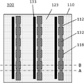
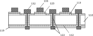
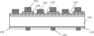
- FIG. 1 is a schematic view showing an example of the back surface of a back electrode type solar cell
- FIG. 2 shows a cross section taken along the alternate long and short dash line A in FIG.
- an emitter region (emitter layer) 112 is formed on the back surface (first main surface) of a semiconductor substrate (for example, a crystalline silicon substrate) 110.
- a base region (base layer) 113 is formed in a stripe shape with the emitter region 112 interposed therebetween, an emitter electrode 122 is formed on the emitter region 112, and a plurality of emitter electrodes 122 are formed as emitter bus bars (for emitters).
- Busbar electrode) 132 is connected.
- a base electrode 123 is formed on the base region 113, and a plurality of base electrodes 123 are connected by a base bus bar (base bus bar electrode) 133.
- the base electrode 123 and the emitter region 112, and the emitter electrode 122 and the base region 113 are electrically insulated by an insulating film 118.
- the solar cell 100 includes a passivation film 119 on the first main surface and the second main surface of the semiconductor substrate 110. In FIG. 1, the passivation film 119 is omitted.
- a resin coating agent is applied to a predetermined location on the substrate by screen printing, ink jet printing, or dispense coating, and completely cured by heat treatment or UV irradiation.
- a resin-cured conductive paste mainly composed of a conductor such as silver, copper, and aluminum to a predetermined location on the substrate by screen printing, inkjet printing, or dispensing, and curing by heat treatment. It was common that.
- Patent Document 1 a polyimide composition is used for the insulating film, and after the insulating film is cured by heating at 140 ° C. for 10 minutes and 250 ° C. for about 30 minutes, a silver paste is printed thereon, and then at 400 ° C.
- the above describes a method of forming an electrode by firing for 30 seconds.
- thermosetting electrode is further laminated and heat-treated after the insulating film is sufficiently cured, not only does the heat treatment take a long time and the productivity is significantly reduced, but also the insulating film There has been a problem that the toughness is reduced due to an excessive amount of heat applied, or that the insulating film contracts and sufficient insulation performance cannot be obtained.
- the present invention has been made in view of the above problems, and an object thereof is to provide a method for producing a solar cell having high productivity and high photoelectric conversion characteristics.
- a manufacturing method is provided.
- Such a method can produce a solar cell with high productivity and high photoelectric conversion characteristics.
- the entire process of curing the conductive paste to form the second electrode is performed simultaneously with the entire process of curing the insulating film precursor to form the insulating film.
- the amount of heat applied to the insulating film precursor during the main curing of the insulating film precursor can be made more appropriate.
- the insulating film is selected from silicone resin, polyamide resin, polyimide resin, polyamideimide resin, fluorine resin, phenol resin, melamine resin, urea resin, polyurethane, epoxy resin, acrylic resin, polyester resin, and poval resin. It is preferable to contain more than one kind of resin.
- the insulating film preferably contains these resins.
- the conductive paste preferably contains one or more kinds of resins selected from epoxy resins, acrylic resins, polyester resins, phenol resins, and silicone resins.
- the conductive paste preferably contains these resins.
- the semiconductor substrate is preferably a crystalline silicon substrate.
- the present invention is particularly suitable for manufacturing a solar cell including a crystalline silicon substrate.
- the solar cell of high photoelectric conversion efficiency will be obtained by a simple process.
- the total time required for curing these materials can be shortened.
- the heat applied to the insulating film precursor can be made more appropriate as compared with the conventional method of forming the second electrode after sufficiently curing the insulating film.
- the toughness of the insulating film is maintained.
- the method of the present invention prevents the problem that the insulating film shrinks and sufficient insulation performance cannot be obtained because it is difficult to apply an excessive amount of heat to the insulating film precursor as compared with the conventional method. it can.
- the present inventors have intensively studied to achieve the above object. as a result, Forming a first electrode on the first main surface of the semiconductor substrate; Applying an insulating film precursor so as to cover at least a part of the first electrode; Pre-curing the insulating film precursor; Applying a conductive paste on at least the insulating film precursor so as to be electrically insulated from the first electrode; Curing the conductive paste to form a second electrode; A step of fully curing the insulating film precursor to form an insulating film; Have The step of applying the conductive paste so as to be electrically insulated from the first electrode is performed after the step of temporarily curing the insulating film precursor, At least part of the step of curing the conductive paste to form a second electrode and at least part of the step of fully curing the insulating film precursor to form an insulating film are performed simultaneously.
- the present inventors have found that a manufacturing method can solve the above-mentioned problems and have completed the present invention.
- the solar cell manufacturing method of the present invention can be applied to the solar cell shown in FIGS.
- a specific solar cell manufacturing method of the present invention will be described with reference to FIGS.
- an N-type semiconductor substrate such as an N-type crystalline silicon substrate is prepared. Specifically, high purity silicon is doped with a pentavalent element such as phosphorus, arsenic, or antimony to prepare an as-cut single crystal ⁇ 100 ⁇ N-type silicon substrate having a specific resistance of 0.1 to 5 ⁇ ⁇ cm. Can do.
- a pentavalent element such as phosphorus, arsenic, or antimony
- an emitter region 112 having a conductivity type opposite to that of the semiconductor substrate 110 and a base region 113 having the same conductivity type as that of the semiconductor substrate 110 are formed on the back surface (first main surface) of the semiconductor substrate 110.
- the formation method of the emitter region 112 and the base region 113 is not particularly limited, and a conventionally known method can be used.
- the emitter region 112 can be formed by vapor phase diffusion using BBr 3 or the like.
- the base region 113 can be formed by vapor phase diffusion using phosphorus oxychloride.
- the emitter region 112 and the base region 113 when forming the emitter region 112 and the base region 113, the emitter region 112 and the base region 113 having desired shapes can be formed by using a diffusion mask made of a silicon oxide film, a silicon nitride film, or the like. .
- a diffusion mask made of a silicon oxide film, a silicon nitride film, or the like.
- a striped base region 113 can be formed, and an emitter region 112 can be formed in a place other than a portion where the base region 113 is formed.
- a passivation film 119 made of a silicon nitride film, a silicon oxide film, or the like is formed on the light receiving surface and the back surface of the semiconductor substrate 110.
- the silicon nitride film can be formed by a CVD method, and the silicon oxide film can be formed by a CVD method or a thermal oxidation method.
- a first electrode is formed on the first main surface of the semiconductor substrate.
- an emitter electrode 122 and a base electrode 123 extending in the horizontal direction are formed as first electrodes on the emitter region 112 and the base region 113.
- the emitter electrode 122 and the base electrode 123 are coated with an Ag paste obtained by mixing Ag powder and glass frit with an organic binder on the emitter region 112 and the base region 113 through the passivation film 119, dried, and then dried. It is formed by baking at a temperature of about 700 to 880 ° C. for about 30 minutes. By this heat treatment, the passivation film 119 is eroded by the Ag paste, and the electrode and silicon are in electrical contact.
- plating may be applied.
- the passivation film 119 at the location is removed by, for example, laser ablation.
- an insulating film precursor is applied so as to cover at least a part of the first electrode.
- the insulating film precursor is applied to the intersection of the emitter region 112 and the base bus bar 133 and the intersection of the base region 113 and the emitter bus bar 132.
- the insulating film precursor becomes an insulating film through temporary curing and main curing described later.
- the insulating film is required to have characteristics such as chemically stable and high usable temperature and easy pattern formation.
- Silicone resin, polyamide resin, polyimide resin, polyamideimide resin, fluororesin, phenol resin A resin mainly composed of melamine resin, urea resin, polyurethane, epoxy resin, acrylic resin, polyester resin, or poval resin can be used. These resins can be used alone or in combination of two or more.
- the method of forming the insulating film precursor from the viewpoint of productivity, a precursor obtained by pasting the resin or the resin raw material with a solvent or the like is used, and this is screen printed or dispensed. Is good.
- the solvent can be appropriately selected according to the resin contained in the insulating film. For example, when forming an insulating film containing a polyimide resin, N-methyl-2-pyrrolidone or the like can be used.
- the insulating film precursor is temporarily cured. Specifically, after printing the paste which is the insulating film precursor, low-temperature heat treatment is performed in the air to temporarily cure the insulating film precursor.
- the temporary curing means that the solvent of the insulating film precursor is volatilized and dried, and at the same time, the insulating film precursor is cured so as not to undergo plastic deformation in the subsequent steps.
- the heat treatment conditions in this case should be optimized depending on the insulating film precursor to be used, but a heat treatment of about 80 ° C. to 200 ° C., preferably about 120 ° C. to 200 ° C. for about 1 minute to 10 minutes is sufficient. There are many cases. If the amount of heat is insufficient, that is, if temporary curing is not achieved at this point, the insulating film precursor is deformed and thinned locally when the electrodes are laminated in the subsequent process, and a short circuit is likely to occur. . Conversely, if the insulating film precursor is fully cured at this point by applying a larger amount of heat, an excessive amount of heat is applied to the insulating film precursor when the electrode is cured in the subsequent process. The precursor shrinks and thins locally, and a short circuit is likely to occur.
- a conductive paste is applied on at least the insulating film precursor so as to be electrically insulated from the first electrode.
- the conductive paste is for forming the second electrode. That is, according to the present invention, the first electrode and the second electrode can be electrically insulated by the insulating film.
- the base bus bar 133 may be used as the second electrode.
- the emitter bus bar 132 can be cited as the second electrode. That is, as shown in FIG. 1, only the first electrode and the second electrode for different conductivity types are electrically insulated by the insulating film, and the first electrode and the second electrode for the same conductivity type are electrically conducted. be able to.
- the second electrode (emitter bus bar 132 and base bus bar 133) is chemically stable and has a high usable temperature and easy pattern formation, silver, copper or aluminum powder is used as an epoxy.
- a resin, an acrylic resin, a polyester resin, a phenol resin, or a silicone resin may be mixed to form a paste, which may be screen printed or dispensed. These resins can be used alone or in combination of two or more.
- the solvent is volatilized and the coating film is dried.
- This drying process is important in preventing leveling of the coating film.
- the heat treatment conditions should be optimized depending on the insulating film precursor to be used, but heat treatment is performed at about 80 to 200 ° C. for about 1 to 3 minutes, and the solvent is volatilized and dried.
- the heat treatment at this time may be a single wafer processing using a hot plate, or a belt furnace or a walking beam furnace may be used.
- the conductive paste is cured to form the second electrode.
- the insulating film precursor is fully cured to form an insulating film.
- at least a part of the process of curing the conductive paste to form the second electrode and at least a part of the process of fully curing the insulating film precursor to form the insulating film are simultaneously performed.
- the substrate is heat-treated in the atmosphere of 200 ° C. to 400 ° C. for about 10 seconds to 5 minutes, and the main curing of the insulating film precursor and the curing of the conductive paste for forming the bus bar are performed simultaneously.
- an in-line apparatus such as a belt furnace or a walking beam furnace is preferably used.
- the main curing of the insulating film precursor starts before reaching the curing temperature of the second electrode.
- part of the process of curing the conductive paste to form the second electrode and part of the process of fully curing the insulating film precursor to form the insulating film are performed simultaneously.
- the entire process of curing the conductive paste to form the second electrode and the insulating film precursor are fully cured to form the insulating film.
- the entire process can be performed simultaneously. In the latter case, the amount of heat applied to the insulating film precursor during the main curing of the insulating film precursor can be made more appropriate.
- the substrate is an N type
- the method of the present invention can also be applied to a case where the substrate is a P type. That is, an N-type layer may be provided as the emitter layer and a P-type layer may be provided as the base layer.
- FIG. 3 is a view showing the back surface of an emitter wrap-through solar cell 300 as another type of solar cell using the present invention.
- the emitter region 112 is formed in an island shape in a region sandwiched between insulating films 118. Yes.
- the emitter region 112 occupies the light receiving surface and communicates with the emitter region 112 on the back surface via a via hole formed in the substrate 110.
- the emitter electrode 122 is also connected to the light receiving surface and the back surface via a via hole.
- a passivation film 119 is formed on the light receiving surface.
- a base bus bar 133 is linearly formed on the base electrode 123 on the back surface of the substrate 110.
- An emitter bus bar 132 is linearly formed on the emitter region 112 and the emitter electrode 122 on the back surface of the substrate 110. However, as shown in FIG. 5, the base electrode 123 is covered with an insulating film 118 in a region where the emitter bus bar 132 as the second electrode and the base electrode 123 as the first electrode intersect.
- Example 1 The solar cell shown in FIGS. 1 and 2 was produced using the method of the present invention.
- a phosphorus-doped ⁇ 100> n-type as-cut silicon substrate having a 150 mm square, a thickness of 200 ⁇ m, and a specific resistance of 1 ⁇ ⁇ cm, an emitter region and a base region were formed on the back surface of the substrate.
- This substrate was heat-treated in an oxygen atmosphere at 900 ° C. for 10 minutes to form silicon oxide films on both sides of the substrate. Subsequently, a silicon nitride film having a thickness of 90 nm was further formed on both surfaces of the substrate by plasma CVD.
- an Ag paste was applied to the emitter region and the base type region by screen printing, and heat treatment was performed at 800 ° C. for 3 seconds to cure the Ag paste, thereby forming an emitter electrode and a base electrode.
- a polyimide paste (HP-1000 manufactured by Hitachi Chemical Co., Ltd.) was applied to a predetermined portion by screen printing, and was temporarily cured by heat treatment on a hot plate at 120 ° C. for 3 minutes.
- thermosetting Ag paste (CA-8590B manufactured by Daiken Chemical Industry) was applied to the back surface of the substrate by screen printing, dried on a hot plate at 170 ° C. for 1 minute, and then heat treated at 300 ° C. for 5 minutes. .
- the emitter bus bar thermosetting Ag paste is applied so as to be electrically insulated from the base electrode, and the base bus bar thermosetting Ag paste is electrically connected to the emitter electrode. (See FIG. 1).
- the polyimide paste and the thermosetting Ag paste were simultaneously cured by the above heat treatment.
- thermosetting Ag paste to form the emitter bus bar and the base bus bar and at least a part of the process of fully curing the polyimide paste to form the insulating film were simultaneously performed.
- a solar battery cell was obtained.
- the output characteristics of the fabricated solar cells were measured using xenon lamp light source type simulated sunlight.
- Example 2 The same substrate as in Example 1 was used, and the formation of the emitter electrode and the base electrode was performed by the same solar cell manufacturing process.
- an epoxy paste (SFX513M1LC manufactured by Shin-Etsu Chemical Co., Ltd.) was applied to a predetermined place by screen printing, and was temporarily cured by heat treatment on a hot plate at 170 ° C. for 1 minute.
- the output characteristics of the fabricated solar cells were measured using xenon lamp light source type simulated sunlight.
- Example 1 The same substrate as in Example 1 was used, and the formation of the emitter electrode and the base electrode was performed by the same solar cell manufacturing process.
- a polyimide paste (HP-1000 manufactured by Hitachi Chemical Co., Ltd.) was applied to a predetermined location by screen printing, and heat-treated on a hot plate at 100 ° C. for 3 minutes and dried. At this time, the polyimide paste was not temporarily cured.
- the output characteristics of the fabricated solar cells were measured using xenon lamp light source type simulated sunlight.
- Example 2 The same substrate as in Example 1 was used, and the formation of the emitter electrode and the base electrode was performed by the same solar cell manufacturing process.
- a polyimide paste (HP-1000 manufactured by Hitachi Chemical Co., Ltd.) is applied to a predetermined location by screen printing, heat-treated on a hot plate at 100 ° C. for 3 minutes and dried, and then heat-treated on a 200 ° C. hot plate for 1 hour. And cured. That is, the polyimide paste was fully cured before applying the thermosetting Ag paste for forming the emitter bus bar and the base bus bar.
- the output characteristics of the fabricated solar cells were measured using xenon lamp light source type simulated sunlight.
- Table 1 shows the solar cell characteristics of Examples 1 and 2 and Comparative Examples 1 and 2.
- Comparative Example 1 the step of applying the conductive paste so as to be electrically insulated from the first electrode is performed after the step of temporarily curing the insulating film precursor.
- Comparative Example 2 at least part of the process of curing the conductive paste to form the second electrode and at least part of the process of fully curing the insulating film precursor to form the insulating film are not performed simultaneously. It was shown that the solar cell characteristics higher than those of Example 1) and a highly efficient solar cell can be realized by a simple process according to the present invention.
- the present invention is not limited to the above embodiment.
- the above-described embodiment is an exemplification, and the present invention has any configuration that has substantially the same configuration as the technical idea described in the claims of the present invention and that exhibits the same effects. Are included in the technical scope.
Landscapes
- Photovoltaic Devices (AREA)
- Life Sciences & Earth Sciences (AREA)
- Engineering & Computer Science (AREA)
- Sustainable Development (AREA)
- Sustainable Energy (AREA)
- Chemical & Material Sciences (AREA)
- Crystallography & Structural Chemistry (AREA)
- Light Receiving Elements (AREA)
- Manufacturing & Machinery (AREA)
Abstract
Description
半導体基板の第1主表面に、第1電極を形成する工程と、
前記第1電極の少なくとも一部を覆うように、絶縁膜前駆体を塗布する工程と、
前記絶縁膜前駆体を仮硬化させる工程と、
少なくとも前記絶縁膜前駆体上に、導電性ペーストを前記第1電極と電気的に絶縁するように塗布する工程と、
前記導電性ペーストを硬化させて第2電極とする工程と、
前記絶縁膜前駆体を本硬化させて絶縁膜とする工程と、
を有し、
前記導電性ペーストを前記第1電極と電気的に絶縁するように塗布する工程は、前記絶縁膜前駆体を仮硬化させる工程後に行われ、
前記導電性ペーストを硬化させて第2電極とする工程の少なくとも一部と前記絶縁膜前駆体を本硬化させて絶縁膜とする工程の少なくとも一部が同時に行われることを特徴とする太陽電池の製造方法を提供する。
半導体基板の第1主表面に、第1電極を形成する工程と、
前記第1電極の少なくとも一部を覆うように、絶縁膜前駆体を塗布する工程と、
前記絶縁膜前駆体を仮硬化させる工程と、
少なくとも前記絶縁膜前駆体上に、導電性ペーストを前記第1電極と電気的に絶縁するように塗布する工程と、
前記導電性ペーストを硬化させて第2電極とする工程と、
前記絶縁膜前駆体を本硬化させて絶縁膜とする工程と、
を有し、
前記導電性ペーストを前記第1電極と電気的に絶縁するように塗布する工程は、前記絶縁膜前駆体を仮硬化させる工程後に行われ、
前記導電性ペーストを硬化させて第2電極とする工程の少なくとも一部と前記絶縁膜前駆体を本硬化させて絶縁膜とする工程の少なくとも一部が同時に行われることを特徴とする太陽電池の製造方法が、上記課題を解決できることを見出し、本発明を完成させた。
本発明の方法を用いて、図1、2に示す太陽電池の作製を行った。
実施例1と同様の基板を使用し、同様の太陽電池製造工程によりエミッタ電極とベース電極の形成までを行った。
実施例1と同様の基板を使用し、同様の太陽電池製造工程によりエミッタ電極とベース電極の形成までを行った。
実施例1と同様の基板を使用し、同様の太陽電池製造工程によりエミッタ電極とベース電極の形成までを行った。

Claims (5)
- 半導体基板の第1主表面に、第1電極を形成する工程と、
前記第1電極の少なくとも一部を覆うように、絶縁膜前駆体を塗布する工程と、
前記絶縁膜前駆体を仮硬化させる工程と、
少なくとも前記絶縁膜前駆体上に、導電性ペーストを前記第1電極と電気的に絶縁するように塗布する工程と、
前記導電性ペーストを硬化させて第2電極とする工程と、
前記絶縁膜前駆体を本硬化させて絶縁膜とする工程と、
を有し、
前記導電性ペーストを前記第1電極と電気的に絶縁するように塗布する工程は、前記絶縁膜前駆体を仮硬化させる工程後に行われ、
前記導電性ペーストを硬化させて第2電極とする工程の少なくとも一部と前記絶縁膜前駆体を本硬化させて絶縁膜とする工程の少なくとも一部が同時に行われることを特徴とする太陽電池の製造方法。 - 前記導電性ペーストを硬化させて第2電極とする工程全体が、前記絶縁膜前駆体を本硬化させて絶縁膜とする工程全体と同時に行われることを特徴とする請求項1に記載の太陽電池の製造方法。
- 前記絶縁膜を、シリコーン樹脂、ポリアミド樹脂、ポリイミド樹脂、ポリアミドイミド樹脂、フッ素樹脂、フェノール樹脂、メラミン樹脂、ユリア樹脂、ポリウレタン、エポキシ樹脂、アクリル樹脂、ポリエステル樹脂及びポバール樹脂から選択される1種類以上の樹脂を含有するものとすることを特徴とする請求項1又は請求項2に記載の太陽電池の製造方法。
- 前記導電性ペーストを、エポキシ樹脂、アクリル樹脂、ポリエステル樹脂、フェノール樹脂及びシリコーン樹脂から選択される1種類以上の樹脂を含有するものとすることを特徴とする請求項1から請求項3のいずれか1項に記載の太陽電池の製造方法。
- 前記半導体基板を、結晶シリコン基板とすることを特徴とする請求項1から請求項4のいずれか1項に記載の太陽電池の製造方法。
Priority Applications (7)
| Application Number | Priority Date | Filing Date | Title |
|---|---|---|---|
| CN201680090581.XA CN110050352B (zh) | 2016-11-07 | 2016-11-07 | 高效率太阳能电池的制造方法 |
| JP2017519714A JP6162918B1 (ja) | 2016-11-07 | 2016-11-07 | 高効率太陽電池の製造方法 |
| PCT/JP2016/004822 WO2018083721A1 (ja) | 2016-11-07 | 2016-11-07 | 高効率太陽電池の製造方法 |
| US15/740,160 US10236397B2 (en) | 2016-11-07 | 2016-11-07 | Method for producing high-efficiency solar cell |
| EP16886807.3A EP3343643B1 (en) | 2016-11-07 | 2016-11-07 | Method for manufacturing high-efficiency solar cell |
| KR1020197012862A KR102556599B1 (ko) | 2016-11-07 | 2016-11-07 | 고효율 태양전지의 제조 방법 |
| TW106107412A TWI635623B (zh) | 2016-11-07 | 2017-03-07 | High-efficiency solar cell manufacturing method |
Applications Claiming Priority (1)
| Application Number | Priority Date | Filing Date | Title |
|---|---|---|---|
| PCT/JP2016/004822 WO2018083721A1 (ja) | 2016-11-07 | 2016-11-07 | 高効率太陽電池の製造方法 |
Publications (1)
| Publication Number | Publication Date |
|---|---|
| WO2018083721A1 true WO2018083721A1 (ja) | 2018-05-11 |
Family
ID=59308950
Family Applications (1)
| Application Number | Title | Priority Date | Filing Date |
|---|---|---|---|
| PCT/JP2016/004822 Ceased WO2018083721A1 (ja) | 2016-11-07 | 2016-11-07 | 高効率太陽電池の製造方法 |
Country Status (7)
| Country | Link |
|---|---|
| US (1) | US10236397B2 (ja) |
| EP (1) | EP3343643B1 (ja) |
| JP (1) | JP6162918B1 (ja) |
| KR (1) | KR102556599B1 (ja) |
| CN (1) | CN110050352B (ja) |
| TW (1) | TWI635623B (ja) |
| WO (1) | WO2018083721A1 (ja) |
Families Citing this family (1)
| Publication number | Priority date | Publication date | Assignee | Title |
|---|---|---|---|---|
| EP3349251B1 (en) * | 2016-11-15 | 2020-04-22 | Shin-Etsu Chemical Co., Ltd | High efficiency solar cell and method for manufacturing high efficiency solar cell |
Citations (4)
| Publication number | Priority date | Publication date | Assignee | Title |
|---|---|---|---|---|
| JP2009253096A (ja) * | 2008-04-08 | 2009-10-29 | Sharp Corp | 太陽電池セルの製造方法および太陽電池モジュールの製造方法ならびに太陽電池モジュール |
| JP2012069594A (ja) | 2010-09-21 | 2012-04-05 | Pi R & D Co Ltd | 太陽電池内の絶縁膜形成用ポリイミド樹脂組成物及びそれを用いた太陽電池内の絶縁膜形成方法 |
| JP2014120554A (ja) * | 2012-12-14 | 2014-06-30 | Sharp Corp | 太陽電池及びその製造方法 |
| WO2016125430A1 (ja) * | 2015-02-05 | 2016-08-11 | 信越化学工業株式会社 | 裏面接合型太陽電池 |
Family Cites Families (15)
| Publication number | Priority date | Publication date | Assignee | Title |
|---|---|---|---|---|
| JP2001345470A (ja) * | 2000-06-01 | 2001-12-14 | Canon Inc | 光起電力素子の製造方法 |
| JP2002057423A (ja) * | 2000-08-07 | 2002-02-22 | Matsushita Electric Ind Co Ltd | 導電性ペーストを用いた回路基板とその製造方法 |
| JP2008306129A (ja) * | 2007-06-11 | 2008-12-18 | Clean Venture 21 Corp | 光電変換装置の製造方法 |
| EP2068369A1 (en) * | 2007-12-03 | 2009-06-10 | Interuniversitair Microelektronica Centrum (IMEC) | Photovoltaic cells having metal wrap through and improved passivation |
| JP2009218490A (ja) * | 2008-03-12 | 2009-09-24 | Citizen Holdings Co Ltd | 太陽電池装置の製造方法 |
| US8158504B2 (en) * | 2008-05-30 | 2012-04-17 | E. I. Du Pont De Nemours And Company | Conductive compositions and processes for use in the manufacture of semiconductor devices—organic medium components |
| US10032940B2 (en) * | 2009-09-18 | 2018-07-24 | Shin-Etsu Chemical Co., Ltd. | Solar cell, method for manufacturing solar cell, and solar cell module |
| US8916410B2 (en) * | 2011-05-27 | 2014-12-23 | Csi Cells Co., Ltd | Methods of manufacturing light to current converter devices |
| ES2582344T3 (es) | 2012-02-23 | 2016-09-12 | Shinmaywa Industries, Ltd. | Método para producir una aguja de punción |
| JP2014045124A (ja) * | 2012-08-28 | 2014-03-13 | Sharp Corp | 太陽電池およびその製造方法、並びに太陽電池モジュールおよびその製造方法 |
| KR101628312B1 (ko) * | 2013-10-31 | 2016-06-09 | 재단법인대구경북과학기술원 | CZTSSe계 박막 태양전지의 제조방법 및 이에 의해 제조된 CZTSSe계 박막 태양전지 |
| US10249775B2 (en) | 2014-06-11 | 2019-04-02 | Shin-Etsu Chemical Co., Ltd. | Solar cell and method for producing solar cell |
| JP6199839B2 (ja) | 2014-09-30 | 2017-09-20 | 信越化学工業株式会社 | 太陽電池及びその製造方法 |
| JP2016219452A (ja) * | 2015-05-14 | 2016-12-22 | 富士通株式会社 | 多層基板及び多層基板の製造方法 |
| KR102599917B1 (ko) | 2016-10-05 | 2023-11-09 | 신에쓰 가가꾸 고교 가부시끼가이샤 | 고광전변환효율 태양전지의 제조방법 및 고광전변환효율 태양전지 |
-
2016
- 2016-11-07 KR KR1020197012862A patent/KR102556599B1/ko active Active
- 2016-11-07 JP JP2017519714A patent/JP6162918B1/ja active Active
- 2016-11-07 US US15/740,160 patent/US10236397B2/en active Active
- 2016-11-07 CN CN201680090581.XA patent/CN110050352B/zh active Active
- 2016-11-07 EP EP16886807.3A patent/EP3343643B1/en active Active
- 2016-11-07 WO PCT/JP2016/004822 patent/WO2018083721A1/ja not_active Ceased
-
2017
- 2017-03-07 TW TW106107412A patent/TWI635623B/zh active
Patent Citations (4)
| Publication number | Priority date | Publication date | Assignee | Title |
|---|---|---|---|---|
| JP2009253096A (ja) * | 2008-04-08 | 2009-10-29 | Sharp Corp | 太陽電池セルの製造方法および太陽電池モジュールの製造方法ならびに太陽電池モジュール |
| JP2012069594A (ja) | 2010-09-21 | 2012-04-05 | Pi R & D Co Ltd | 太陽電池内の絶縁膜形成用ポリイミド樹脂組成物及びそれを用いた太陽電池内の絶縁膜形成方法 |
| JP2014120554A (ja) * | 2012-12-14 | 2014-06-30 | Sharp Corp | 太陽電池及びその製造方法 |
| WO2016125430A1 (ja) * | 2015-02-05 | 2016-08-11 | 信越化学工業株式会社 | 裏面接合型太陽電池 |
Non-Patent Citations (1)
| Title |
|---|
| See also references of EP3343643A4 |
Also Published As
| Publication number | Publication date |
|---|---|
| CN110050352A (zh) | 2019-07-23 |
| EP3343643A1 (en) | 2018-07-04 |
| CN110050352B (zh) | 2022-04-29 |
| JP6162918B1 (ja) | 2017-07-12 |
| EP3343643B1 (en) | 2021-08-04 |
| EP3343643A4 (en) | 2019-01-23 |
| KR20190076975A (ko) | 2019-07-02 |
| TW201818567A (zh) | 2018-05-16 |
| JPWO2018083721A1 (ja) | 2018-11-01 |
| US10236397B2 (en) | 2019-03-19 |
| KR102556599B1 (ko) | 2023-07-17 |
| TWI635623B (zh) | 2018-09-11 |
| US20180315869A1 (en) | 2018-11-01 |
Similar Documents
| Publication | Publication Date | Title |
|---|---|---|
| CN106575679B (zh) | 太阳能电池及其制造方法 | |
| US10249775B2 (en) | Solar cell and method for producing solar cell | |
| US20110030759A1 (en) | Method for manufacturing solar cell, method for manufacturing solar cell module, and solar cell module | |
| JP6162918B1 (ja) | 高効率太陽電池の製造方法 | |
| WO2013161373A1 (ja) | 太陽電池およびその製造方法 | |
| JP2016530727A (ja) | 太陽電池の製造方法 | |
| KR100552957B1 (ko) | 효율이 개선된 태양전지 및 메탈입자를 이용한 그의제조방법 | |
| WO2018092172A1 (ja) | 高効率太陽電池及び高効率太陽電池の製造方法 | |
| JP6875252B2 (ja) | ポリイミドペーストの乾燥方法及び高光電変換効率太陽電池の製造方法 | |
| JP6405285B2 (ja) | 太陽電池の製造方法 | |
| JP6532518B2 (ja) | 高効率太陽電池の製造方法 | |
| CN113363346A (zh) | 背接触型太阳能电池单元的制造方法 | |
| HK1096196B (en) | Functional paste |
Legal Events
| Date | Code | Title | Description |
|---|---|---|---|
| WWE | Wipo information: entry into national phase |
Ref document number: 2017519714 Country of ref document: JP |
|
| REEP | Request for entry into the european phase |
Ref document number: 2016886807 Country of ref document: EP |
|
| WWE | Wipo information: entry into national phase |
Ref document number: 15740160 Country of ref document: US |
|
| 121 | Ep: the epo has been informed by wipo that ep was designated in this application |
Ref document number: 16886807 Country of ref document: EP Kind code of ref document: A1 |
|
| ENP | Entry into the national phase |
Ref document number: 20197012862 Country of ref document: KR Kind code of ref document: A |
|
| NENP | Non-entry into the national phase |
Ref country code: DE |