WO2018116867A1 - アンテナ基板 - Google Patents
アンテナ基板 Download PDFInfo
- Publication number
- WO2018116867A1 WO2018116867A1 PCT/JP2017/044148 JP2017044148W WO2018116867A1 WO 2018116867 A1 WO2018116867 A1 WO 2018116867A1 JP 2017044148 W JP2017044148 W JP 2017044148W WO 2018116867 A1 WO2018116867 A1 WO 2018116867A1
- Authority
- WO
- WIPO (PCT)
- Prior art keywords
- insulating layer
- substrate
- antenna
- connection pad
- opening
- Prior art date
- Legal status (The legal status is an assumption and is not a legal conclusion. Google has not performed a legal analysis and makes no representation as to the accuracy of the status listed.)
- Ceased
Links
Images


Classifications
-
- H—ELECTRICITY
- H01—ELECTRIC ELEMENTS
- H01Q—ANTENNAS, i.e. RADIO AERIALS
- H01Q1/00—Details of, or arrangements associated with, antennas
- H01Q1/27—Adaptation for use in or on movable bodies
- H01Q1/32—Adaptation for use in or on road or rail vehicles
- H01Q1/3208—Adaptation for use in or on road or rail vehicles characterised by the application wherein the antenna is used
- H01Q1/3233—Adaptation for use in or on road or rail vehicles characterised by the application wherein the antenna is used particular used as part of a sensor or in a security system, e.g. for automotive radar, navigation systems
-
- H—ELECTRICITY
- H01—ELECTRIC ELEMENTS
- H01Q—ANTENNAS, i.e. RADIO AERIALS
- H01Q21/00—Antenna arrays or systems
- H01Q21/06—Arrays of individually energised antenna units similarly polarised and spaced apart
- H01Q21/061—Two dimensional planar arrays
- H01Q21/065—Patch antenna array
-
- H—ELECTRICITY
- H01—ELECTRIC ELEMENTS
- H01Q—ANTENNAS, i.e. RADIO AERIALS
- H01Q1/00—Details of, or arrangements associated with, antennas
- H01Q1/12—Supports; Mounting means
- H01Q1/22—Supports; Mounting means by structural association with other equipment or articles
- H01Q1/2283—Supports; Mounting means by structural association with other equipment or articles mounted in or on the surface of a semiconductor substrate as a chip-type antenna or integrated with other components into an IC package
-
- H—ELECTRICITY
- H01—ELECTRIC ELEMENTS
- H01Q—ANTENNAS, i.e. RADIO AERIALS
- H01Q1/00—Details of, or arrangements associated with, antennas
- H01Q1/36—Structural form of radiating elements, e.g. cone, spiral, umbrella; Particular materials used therewith
- H01Q1/38—Structural form of radiating elements, e.g. cone, spiral, umbrella; Particular materials used therewith formed by a conductive layer on an insulating support
-
- H—ELECTRICITY
- H01—ELECTRIC ELEMENTS
- H01Q—ANTENNAS, i.e. RADIO AERIALS
- H01Q21/00—Antenna arrays or systems
- H01Q21/06—Arrays of individually energised antenna units similarly polarised and spaced apart
-
- H—ELECTRICITY
- H01—ELECTRIC ELEMENTS
- H01Q—ANTENNAS, i.e. RADIO AERIALS
- H01Q9/00—Electrically-short antennas having dimensions not more than twice the operating wavelength and consisting of conductive active radiating elements
- H01Q9/04—Resonant antennas
- H01Q9/0407—Substantially flat resonant element parallel to ground plane, e.g. patch antenna
- H01Q9/0414—Substantially flat resonant element parallel to ground plane, e.g. patch antenna in a stacked or folded configuration
-
- H—ELECTRICITY
- H05—ELECTRIC TECHNIQUES NOT OTHERWISE PROVIDED FOR
- H05K—PRINTED CIRCUITS; CASINGS OR CONSTRUCTIONAL DETAILS OF ELECTRIC APPARATUS; MANUFACTURE OF ASSEMBLAGES OF ELECTRICAL COMPONENTS
- H05K1/00—Printed circuits
- H05K1/02—Details
- H05K1/14—Structural association of two or more printed circuits
-
- H—ELECTRICITY
- H05—ELECTRIC TECHNIQUES NOT OTHERWISE PROVIDED FOR
- H05K—PRINTED CIRCUITS; CASINGS OR CONSTRUCTIONAL DETAILS OF ELECTRIC APPARATUS; MANUFACTURE OF ASSEMBLAGES OF ELECTRICAL COMPONENTS
- H05K1/00—Printed circuits
- H05K1/02—Details
- H05K1/14—Structural association of two or more printed circuits
- H05K1/144—Stacked arrangements of planar printed circuit boards
Definitions
- the present disclosure relates to an antenna substrate.
- Patent Document 1 describes that an antenna substrate includes a spacer and two mounting substrates, and each mounting substrate is arranged above and below the spacer.
- the antenna substrate of the present disclosure includes a cap substrate, a frame substrate, and a base substrate.
- the cap substrate includes a first insulating layer, a plurality of first antenna conductors arranged vertically and horizontally in a state where the upper and lower surfaces of the first insulating layer face each other via the first insulating layer, and the first insulating layer A first connection pad located on the outer peripheral edge of the lower surface of the insulating layer is included.
- the frame substrate includes a second insulating layer, a second connection pad positioned on the outer peripheral edge of the upper surface of the second insulating layer, and a third connection pad positioned on the outer peripheral edge of the lower surface of the second insulating layer. It is out.
- the base substrate includes a third insulating layer, a plurality of second antenna conductors located on the upper surface of the third insulating layer, and a fourth connection pad located on the outer peripheral edge of the upper surface of the third insulating layer. It is out.
- the first connection pad and the second connection pad are connected to each other, the third connection pad and the fourth connection pad are connected to each other, and the base substrate, the frame substrate, and the cap substrate are sequentially stacked.
- the second insulating layer has a first opening having an outer periphery located outside the outer periphery of the first antenna conductor in a top view. The first opening is positioned so as to surround the outer periphery of the first antenna conductor.
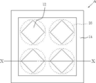
- FIG. 1A is a schematic top view illustrating a first exemplary embodiment of an antenna substrate according to the present disclosure.
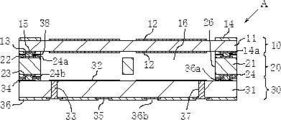
- 1B is a schematic cross-sectional view taken along the line XX shown in FIG. 1A.
- FIG. 2 is a schematic top view illustrating the second embodiment of the antenna substrate of the present disclosure.
- FIG. 3 is a schematic top view illustrating the third embodiment of the antenna substrate of the present disclosure.
- FIG. 1A is a top view illustrating an exemplary embodiment of an antenna substrate A of the present disclosure.
- 1B is a cross-sectional view taken along the line XX shown in FIG. 1A.
- the antenna substrate A includes a cap substrate 10, a frame substrate 20, and a base substrate 30.
- the antenna substrate A includes a stacked body (no symbol) sequentially stacked from the top in the order of the cap substrate 10, the frame substrate 20, and the base substrate 30.
- the laminated body ensures the mechanical strength of the antenna substrate A.
- the cap substrate 10 has a first insulating layer 11, a first antenna conductor 12, a first connection pad 13, and a solder resist layer 14.
- a plurality of first antenna conductors 12 are formed at the center of the upper and lower surfaces of the first insulating layer 11.
- the first antenna conductors 12 are arranged vertically and horizontally so as to face each other with the first insulating layer 11 in between. That is, a plurality of first antenna conductors 12 are formed on the upper and lower surfaces of the first insulating layer 11 when viewed from above.
- the first insulation among the plurality of first antenna conductors 12 on the upper surface of the first insulating layer 11 and the plurality of first antenna conductors 12 on the lower surface of the first insulating layer 11 is used.
- Those facing each other through the layer 11 are formed in the same shape and size.
- a plurality of first connection pads 13 are formed on the outer peripheral edge of the lower surface of the first insulating layer 11. Further, a solder resist layer 14 is formed on the outer peripheral edge of the upper and lower surfaces of the first insulating layer 11. The first connection pad 13 is exposed in the opening 14 a provided in the solder resist layer 14.
- the frame substrate 20 has a second insulating layer 21, a second connection pad 22, a third connection pad 23, and a solder resist layer 24.
- the second insulating layer 21 includes a first opening 26 having an outer periphery located outside the outer periphery of the first antenna conductor 12 in a top view.
- a plurality of first openings 26 are provided in the second insulating layer 21.
- Each of the plurality of first openings 26 is arranged so that the first antenna conductor 12 is accommodated inside each of the first opening portions 26 when viewed from above (when viewed from the top).
- the first opening 26 is sandwiched between the cap substrate 10 and the base substrate 30 to form the cavity 16.
- the cavity 16 functions as a path for transmitting and receiving electromagnetic waves for signals between the first antenna conductor 12 and the second antenna conductor 32.
- the distance between the first antenna conductor 12 and the second antenna conductor 32 is adjusted to an optimum distance for transmitting and receiving signal electromagnetic waves by adjusting the thickness of the second insulating layer 21. Can do.
- a plurality of second connection pads 22 are formed on the outer peripheral edge of the upper surface of the second insulating layer 21.
- a plurality of third connection pads 23 are formed on the outer peripheral edge of the lower surface of the second insulating layer 21.
- a solder resist layer 24 is formed on the outer peripheral edges of the upper and lower surfaces of the second insulating layer 21.
- the second connection pad 22 is exposed in the opening 24 a provided in the solder resist layer 24.
- the third connection pad 23 is exposed in the opening 24 b provided in the solder resist layer 24.
- the second connection pad 22 and the first connection pad 13 are connected via the solder 15.
- the first connection pad 13 and the second connection pad 22 not only physically connect the cap substrate 10 and the frame substrate 20 but also can be electrically connected. Thereby, the cap substrate 10 is laminated on the frame substrate 20.
- the base substrate 30 has a third insulating layer 31, a second antenna conductor 32, a conductor layer 33, a fourth connection pad 34, an electrode 35, and a solder resist layer 36.
- a plurality of second antenna conductors 32 are arranged on the upper surface of the third insulating layer 31.
- the second antenna conductor 32 is disposed at a position facing the first antenna conductor 12.
- the first opening 26 is provided corresponding to the first antenna conductor 12. Therefore, in the cavity 16, each second antenna conductor 32 directly faces the first antenna conductor 12 with a space (such as air in the cavity 16) interposed therebetween.
- the third insulating layer 31 has a plurality of through holes 37 penetrating vertically.
- a conductor layer 33 is formed on the surface of the third insulating layer 31 and inside the through hole 37. A part of the conductor layer 33 is connected to the second antenna conductor 32.
- a plurality of fourth connection pads 34 are formed on the outer peripheral edge of the upper surface of the third insulating layer 31.
- the fourth connection pad 34 is connected to the third connection pad 23 via the solder 15.
- the frame substrate 20 is stacked on the base substrate 30.
- the third connection pad 23 and the fourth connection pad 34 can not only physically connect the frame substrate 20 and the base substrate 30 but also electrically connect them.
- a plurality of electrodes 35 are formed on the lower surface of the third insulating layer 31.
- the electrode 35 is connected via an electrode of the external electric substrate and solder. Thereby, the antenna substrate A is electrically connected to the external electric substrate.
- a solder resist layer 36 is formed on part of the upper and lower surfaces of the third insulating layer 31.
- the solder resist layer 36 has an opening 36 a that exposes the fourth connection pad 34.
- the solder resist layer 36 has an opening 36 b that exposes the electrode 35.
- the antenna substrate A is configured in such a manner that the frame substrate 20 and the cap substrate 10 are sequentially stacked above the base substrate 30.
- the antenna substrate A has the following functions, for example.
- a signal transmitted from the external electric board is transmitted to the second antenna conductor 32 through the electrode 35 and the conductor layer 33.
- the second antenna conductor 32 receiving the signal radiates electromagnetic waves.
- the radiated electromagnetic wave propagates in the cavity 16 and sequentially propagates to the first antenna conductor 12 on the lower surface side of the first insulating layer 11 and the first antenna conductor 12 on the upper surface side.
- the first antenna conductor 12 on the upper surface side radiates electromagnetic waves toward the outside.
- the first antenna conductor 12 has a function of transmitting an electromagnetic wave received from outside as a signal to the external electric board along the reverse path.
- the outer periphery of the first opening 26 forming the cavity 16 is arranged to be located outside the outer periphery of the first antenna conductor 12 for transmitting and receiving electromagnetic waves. It is necessary to secure a route.
- the distance between the first antenna conductor 12 and the second antenna conductor 32 is kept constant, so that stable electromagnetic wave transmission / reception can be performed between them.
- the gap between the connection part between the cap substrate 10 and the frame substrate 20 and the gap between the connection part between the frame substrate 20 and the base substrate 30 are filled with a sealing resin 38.
- the sealing resin 38 firmly bonds the cap substrate 10, the frame substrate 20, and the base substrate 30. Further, the sealing resin 38 reduces the intrusion of moisture or foreign matter into the cavity 16 from the gap. Thereby, the second antenna conductor 32 in the cavity 16 is protected from the external environment.
- the first to third insulating layers 11, 21, and 31 are, for example, electrical insulating materials obtained by flatly thermosetting a glass cloth impregnated with a thermosetting resin such as epoxy resin or bismaleimide triazine resin under heat and pressure. Made of material.
- the first opening 26 is formed by drilling, for example. By drilling the first opening 26 into a circular shape, it is possible to improve the position accuracy or the processing speed.
- the through hole 37 is formed by, for example, drilling, laser processing, or blasting.
- the first and second antenna conductors 12, 32, the first to fourth connection pads 13, 22, 23, 34, and the conductor layer 33 are made of a highly conductive metal such as copper plating by a known plating technique, for example. Is formed.
- the solder resist layers 14, 24, and 36 are made of an electrically insulating material formed in a predetermined pattern by exposing and developing a thermosetting resin having photosensitivity such as an acrylic-modified epoxy resin on the surface of the insulating layer. Become.
- connection of the cap substrate 10, the frame substrate 20 and the base substrate 30 is performed as follows, for example.
- solder 15 is welded to at least one of the first connection pad 13 and the second connection pad 22 and at least one of the third connection pad 23 and the fourth connection pad 34.
- the frame substrate 20 is placed on the base substrate 30 with the first connection pad 13 and the second connection pad 22, and the third connection pad 23 and the fourth connection pad 34 facing each other.
- the cap substrate 10 is placed on the frame substrate 20.
- thermosetting sealing resin 38 is filled in the gap between the connection portion between the cap substrate 10 and the frame substrate 20 and the gap between the connection portion between the frame substrate 20 and the base substrate 30 and thermally cured. Thereby, the cap substrate 10, the frame substrate 20, and the base substrate 30 are firmly bonded.
- the second insulating layer 21 has an outer periphery located outside the outer periphery of the first antenna conductor 12 in a top view, for example, a circular first The opening 26 is provided.
- the interval between the adjacent first openings 26 is narrow.
- a portion of the first insulating layer 11 around the first opening 26 surrounding each first antenna conductor 12 has a function of improving the mechanical strength of the antenna substrate A. ing.
- the present disclosure is particularly effective in the case where the first antenna conductors 12 adjacent to each other are arranged in a state in which the respective corners face each other as shown in FIG. 1A.
- the second insulating layer 21 has the first opening 26 having an outer periphery located outside the outer periphery of the first antenna conductor 12 in a top view. ing.
- the first openings 26 are arranged so as to individually surround the outer periphery of the first antenna conductor 12. For this reason, the part where the space
- the antenna substrate A can be provided.
- the second insulating layer 21 may include a connecting portion 27 that connects the first openings 26.
- the connecting portion 27 penetrates the second insulating layer 21 in the thickness direction.
- the connecting portion 27 may contribute to improving the workability of the first opening portion 26.
- the outer diameter of the connecting portion 27 (the width of the connecting portion 27 in the direction orthogonal to the direction in which the connecting portion 27 extends) is smaller than the outer diameter or diameter of the first opening 26 in this direction.
- the case where only the first opening 26 is formed in the second insulating layer 21 is shown.
- the second opening 28 may be formed between the openings 26 and between the first opening 26 and the outer periphery of the second insulating layer 21. Further, the second opening 28 may be formed only between the first openings 26, and only between the first opening 26 and the outer periphery of the second insulating layer 21. It doesn't matter.
- the second opening 28 is arranged in a state where it does not connect to the connecting portion 27.
- the size of the second opening 28 may be larger than the size of the first opening.
- the shape of the second opening 28 may be not only a circular shape but also a polygonal shape, an oval shape, or an elliptical shape.
- the shape of the second opening 28 may be a shape in which a notch or the like is provided in a circular, polygonal, oval, or elliptical opening.
- the second opening 28 has a function of further reducing deformation of the antenna substrate A by balancing the rigidity of the second insulating layer 21.
- the shape of the first opening 26 is a circular shape that can be easily drilled, such as the above-described drilling, is illustrated.
- it may be similar to the shape of the first antenna conductor 12.
- interval of adjacent 1st opening parts 26 becomes narrower further decreases.
- deformation of the antenna substrate A is further reduced by improving the rigidity of the second insulating layer 21.
Landscapes
- Engineering & Computer Science (AREA)
- Microelectronics & Electronic Packaging (AREA)
- Computer Security & Cryptography (AREA)
- Radar, Positioning & Navigation (AREA)
- Remote Sensing (AREA)
- Details Of Aerials (AREA)
- Variable-Direction Aerials And Aerial Arrays (AREA)
- Combinations Of Printed Boards (AREA)
- Waveguide Aerials (AREA)
Abstract
Description
11 第1の絶縁層
12 第1のアンテナ用導体
13 第1の接続パッド
20 フレーム基板
21 第2の絶縁層
22 第2の接続パッド
23 第3の接続パッド
26 第1の開口部
30 ベース基板
31 第3の絶縁層
32 第2のアンテナ用導体
34 第4の接続パッド
A アンテナ基板
Claims (8)
- 第1の絶縁層、該第1の絶縁層の上下両面に該第1の絶縁層を介して互いに対向する状態で縦横の並びに位置する複数の第1のアンテナ用導体、および前記第1の絶縁層の下面の外周縁に位置する第1の接続パッドを有するキャップ基板と、
第2の絶縁層、該第2の絶縁層の上面の外周縁に位置する第2の接続パッド、および前記第2の絶縁層の下面の外周縁に位置する第3の接続パッドを有するフレーム基板と、
第3の絶縁層、該第3の絶縁層の上面に配設された複数の第2のアンテナ用導体、および前記第3の絶縁層の上面の外周縁に位置する第4の接続パッドを有するベース基板と、を備えているとともに、
前記第1の接続パッドと前記第2の接続パッドとが互いに接続され、
前記第3の接続パッドと前記第4の接続パッドとが互いに接続されて、前記ベース基板と前記フレーム基板と前記キャップ基板とが順次積層されており、
前記第2の絶縁層は、上面視において前記第1のアンテナ用導体の外周よりも外側に位置する外周を有する複数の第1の開口部を有し、該第1の開口部は、前記第1のアンテナ用導体の外周を囲む状態に位置していることを特徴とするアンテナ基板。 - 前記第1の開口部同士の間に、該第1の開口部同士をつなぐ連結部を備えていることを特徴とする請求項1に記載のアンテナ基板。
- 前記第1の開口部が、円形状であることを特徴とする請求項1または請求項2のいずれかに記載のアンテナ基板。
- 前記第2の絶縁層は、前記第1の開口部同士の間、および前記第1の開口部と前記第2の絶縁層の外周との間の少なくともいずれかに、第2の開口部を有していることを特徴とする請求項1に記載のアンテナ基板。
- 前記第2の開口部が、円形状であることを特徴とする請求項4に記載のアンテナ基板。
- 前記第1の絶縁層の上面の複数の前記第1のアンテナ用導体と、前記第1の絶縁層の下面の複数の前記第1のアンテナ用導体と、のうち第1の絶縁層を介して互いに対向し合うものは、互いに同じ形状および寸法であることを特徴とする請求項1に記載のアンテナ基板。
- 前記第1の開口部は、前記キャップ基板と前記ベース基板とに挟まれてキャビティとなることを特徴とする請求項1に記載のアンテナ基板。
- 前記第1の開口部は、前記第1のアンテナ用導体の外周を個々に囲む状態に位置していることを特徴とする請求項1に記載のアンテナ基板。
Priority Applications (6)
| Application Number | Priority Date | Filing Date | Title |
|---|---|---|---|
| JP2018557672A JP6749061B2 (ja) | 2016-12-22 | 2017-12-08 | アンテナ基板 |
| EP17883463.6A EP3561955B1 (en) | 2016-12-22 | 2017-12-08 | Antenna substrate |
| CN201780075166.1A CN110050386B (zh) | 2016-12-22 | 2017-12-08 | 天线基板 |
| US16/468,711 US10868368B2 (en) | 2016-12-22 | 2017-12-08 | Antenna substrate |
| KR1020197016035A KR102084450B1 (ko) | 2016-12-22 | 2017-12-08 | 안테나 기판 |
| FIEP17883463.6T FI3561955T3 (fi) | 2016-12-22 | 2017-12-08 | Antennialusta |
Applications Claiming Priority (2)
| Application Number | Priority Date | Filing Date | Title |
|---|---|---|---|
| JP2016248789 | 2016-12-22 | ||
| JP2016-248789 | 2016-12-22 |
Publications (1)
| Publication Number | Publication Date |
|---|---|
| WO2018116867A1 true WO2018116867A1 (ja) | 2018-06-28 |
Family
ID=62627801
Family Applications (1)
| Application Number | Title | Priority Date | Filing Date |
|---|---|---|---|
| PCT/JP2017/044148 Ceased WO2018116867A1 (ja) | 2016-12-22 | 2017-12-08 | アンテナ基板 |
Country Status (8)
| Country | Link |
|---|---|
| US (1) | US10868368B2 (ja) |
| EP (1) | EP3561955B1 (ja) |
| JP (1) | JP6749061B2 (ja) |
| KR (1) | KR102084450B1 (ja) |
| CN (1) | CN110050386B (ja) |
| FI (1) | FI3561955T3 (ja) |
| TW (1) | TWI653785B (ja) |
| WO (1) | WO2018116867A1 (ja) |
Cited By (1)
| Publication number | Priority date | Publication date | Assignee | Title |
|---|---|---|---|---|
| US11705625B2 (en) | 2020-06-04 | 2023-07-18 | Tdk Corporation | Antenna device |
Families Citing this family (4)
| Publication number | Priority date | Publication date | Assignee | Title |
|---|---|---|---|---|
| KR102731798B1 (ko) | 2019-12-10 | 2024-11-19 | 삼성전기주식회사 | 안테나 기판 및 이를 포함하는 안테나 모듈 |
| CN219513349U (zh) * | 2020-08-19 | 2023-08-11 | 株式会社村田制作所 | 通信装置 |
| KR20220066536A (ko) | 2020-11-16 | 2022-05-24 | 삼성전기주식회사 | 안테나 장치 |
| TWI784527B (zh) * | 2021-05-19 | 2022-11-21 | 啟碁科技股份有限公司 | 陣列天線裝置及其天線單元 |
Citations (6)
| Publication number | Priority date | Publication date | Assignee | Title |
|---|---|---|---|---|
| JPH02256305A (ja) * | 1988-12-24 | 1990-10-17 | Kojima Press Co Ltd | マイクロストリップアンテナ |
| JPH0998016A (ja) * | 1995-10-02 | 1997-04-08 | Mitsubishi Electric Corp | マイクロストリップアンテナ |
| JP2000138525A (ja) * | 1998-10-30 | 2000-05-16 | Mitsubishi Electric Corp | マイクロストリップアンテナおよびマイクロストリップアンテナ基板 |
| JP2004327641A (ja) | 2003-04-24 | 2004-11-18 | Tdk Corp | 電子部品モジュール |
| JP2012235351A (ja) * | 2011-05-02 | 2012-11-29 | Denso Corp | アンテナ装置 |
| JP2016066699A (ja) * | 2014-09-25 | 2016-04-28 | 京セラサーキットソリューションズ株式会社 | 複合配線基板およびその実装構造体 |
Family Cites Families (11)
| Publication number | Priority date | Publication date | Assignee | Title |
|---|---|---|---|---|
| JP3939504B2 (ja) * | 2001-04-17 | 2007-07-04 | カシオ計算機株式会社 | 半導体装置並びにその製造方法および実装構造 |
| FR2882491B1 (fr) * | 2005-02-23 | 2009-04-24 | Eads Space Transp Sas Soc Par | Procede pour former des motifs electriquement conducteurs sur une surface non developpable d'un substrat isolant, et dispositif obtenu |
| KR20090047015A (ko) * | 2007-11-07 | 2009-05-12 | 위월드 주식회사 | 개선된 원편파 수신용 도파관 슬롯 배열 안테나 |
| JP2014179472A (ja) * | 2013-03-15 | 2014-09-25 | Murata Mfg Co Ltd | モジュールおよびその製造方法 |
| US9172131B2 (en) * | 2013-03-15 | 2015-10-27 | Advanced Semiconductor Engineering, Inc. | Semiconductor structure having aperture antenna |
| TW201503777A (zh) * | 2013-05-30 | 2015-01-16 | 京瓷Slc技術股份有限公司 | 配線基板 |
| JP2015139051A (ja) * | 2014-01-21 | 2015-07-30 | 日立金属株式会社 | アンテナ装置 |
| US9620464B2 (en) * | 2014-08-13 | 2017-04-11 | International Business Machines Corporation | Wireless communications package with integrated antennas and air cavity |
| CN109983619B (zh) * | 2016-12-20 | 2020-09-01 | 京瓷株式会社 | 天线模块 |
| TWI653780B (zh) * | 2016-12-22 | 2019-03-11 | 日商京瓷股份有限公司 | 天線基板及其製造方法 |
| CN108879114A (zh) * | 2017-05-16 | 2018-11-23 | 华为技术有限公司 | 集成天线封装结构和终端 |
-
2017
- 2017-12-04 TW TW106142375A patent/TWI653785B/zh active
- 2017-12-08 EP EP17883463.6A patent/EP3561955B1/en active Active
- 2017-12-08 KR KR1020197016035A patent/KR102084450B1/ko active Active
- 2017-12-08 US US16/468,711 patent/US10868368B2/en active Active
- 2017-12-08 CN CN201780075166.1A patent/CN110050386B/zh active Active
- 2017-12-08 FI FIEP17883463.6T patent/FI3561955T3/fi active
- 2017-12-08 WO PCT/JP2017/044148 patent/WO2018116867A1/ja not_active Ceased
- 2017-12-08 JP JP2018557672A patent/JP6749061B2/ja active Active
Patent Citations (6)
| Publication number | Priority date | Publication date | Assignee | Title |
|---|---|---|---|---|
| JPH02256305A (ja) * | 1988-12-24 | 1990-10-17 | Kojima Press Co Ltd | マイクロストリップアンテナ |
| JPH0998016A (ja) * | 1995-10-02 | 1997-04-08 | Mitsubishi Electric Corp | マイクロストリップアンテナ |
| JP2000138525A (ja) * | 1998-10-30 | 2000-05-16 | Mitsubishi Electric Corp | マイクロストリップアンテナおよびマイクロストリップアンテナ基板 |
| JP2004327641A (ja) | 2003-04-24 | 2004-11-18 | Tdk Corp | 電子部品モジュール |
| JP2012235351A (ja) * | 2011-05-02 | 2012-11-29 | Denso Corp | アンテナ装置 |
| JP2016066699A (ja) * | 2014-09-25 | 2016-04-28 | 京セラサーキットソリューションズ株式会社 | 複合配線基板およびその実装構造体 |
Non-Patent Citations (1)
| Title |
|---|
| See also references of EP3561955A4 |
Cited By (1)
| Publication number | Priority date | Publication date | Assignee | Title |
|---|---|---|---|---|
| US11705625B2 (en) | 2020-06-04 | 2023-07-18 | Tdk Corporation | Antenna device |
Also Published As
| Publication number | Publication date |
|---|---|
| CN110050386A (zh) | 2019-07-23 |
| EP3561955B1 (en) | 2023-03-15 |
| TW201830769A (zh) | 2018-08-16 |
| US10868368B2 (en) | 2020-12-15 |
| JPWO2018116867A1 (ja) | 2019-10-24 |
| US20190319350A1 (en) | 2019-10-17 |
| KR102084450B1 (ko) | 2020-03-04 |
| KR20190073550A (ko) | 2019-06-26 |
| JP6749061B2 (ja) | 2020-09-02 |
| TWI653785B (zh) | 2019-03-11 |
| FI3561955T3 (fi) | 2023-04-21 |
| CN110050386B (zh) | 2020-11-10 |
| EP3561955A4 (en) | 2020-08-12 |
| EP3561955A1 (en) | 2019-10-30 |
Similar Documents
| Publication | Publication Date | Title |
|---|---|---|
| US10512153B2 (en) | High frequency circuit | |
| JP6749062B2 (ja) | アンテナ基板およびその製造方法 | |
| JP6749061B2 (ja) | アンテナ基板 | |
| JP6299878B2 (ja) | 高周波通信モジュール及び高周波通信装置 | |
| JP6397127B2 (ja) | 半導体素子パッケージ、半導体装置および実装構造体 | |
| US20180146302A1 (en) | Mems microphone package structure and method for manufacturing the mems microphone package structures | |
| US20140353026A1 (en) | Wiring board | |
| WO2021230215A1 (ja) | 高周波回路 | |
| JP6139585B2 (ja) | 高周波モジュール及びマイクロ波送受信装置 | |
| US9635753B2 (en) | Wiring board | |
| US11464104B2 (en) | Wiring substrate | |
| JP2019029396A (ja) | 電子装置 | |
| JP2016119596A (ja) | サーキュレータおよびサーキュレータの製造方法 | |
| JP2021078003A (ja) | 無線モジュール | |
| JP2005159125A (ja) | 配線基板 | |
| JP2017220790A (ja) | アンテナ基板およびアンテナ装置 |
Legal Events
| Date | Code | Title | Description |
|---|---|---|---|
| 121 | Ep: the epo has been informed by wipo that ep was designated in this application |
Ref document number: 17883463 Country of ref document: EP Kind code of ref document: A1 |
|
| ENP | Entry into the national phase |
Ref document number: 2018557672 Country of ref document: JP Kind code of ref document: A Ref document number: 20197016035 Country of ref document: KR Kind code of ref document: A |
|
| NENP | Non-entry into the national phase |
Ref country code: DE |
|
| ENP | Entry into the national phase |
Ref document number: 2017883463 Country of ref document: EP Effective date: 20190722 |