WO2018128193A1 - 六方晶窒化ホウ素薄膜とその製造方法 - Google Patents
六方晶窒化ホウ素薄膜とその製造方法 Download PDFInfo
- Publication number
- WO2018128193A1 WO2018128193A1 PCT/JP2018/000107 JP2018000107W WO2018128193A1 WO 2018128193 A1 WO2018128193 A1 WO 2018128193A1 JP 2018000107 W JP2018000107 W JP 2018000107W WO 2018128193 A1 WO2018128193 A1 WO 2018128193A1
- Authority
- WO
- WIPO (PCT)
- Prior art keywords
- thin film
- boron nitride
- hexagonal boron
- metal
- nitride thin
- Prior art date
- Legal status (The legal status is an assumption and is not a legal conclusion. Google has not performed a legal analysis and makes no representation as to the accuracy of the status listed.)
- Ceased
Links
Images


Classifications
-
- C—CHEMISTRY; METALLURGY
- C23—COATING METALLIC MATERIAL; COATING MATERIAL WITH METALLIC MATERIAL; CHEMICAL SURFACE TREATMENT; DIFFUSION TREATMENT OF METALLIC MATERIAL; COATING BY VACUUM EVAPORATION, BY SPUTTERING, BY ION IMPLANTATION OR BY CHEMICAL VAPOUR DEPOSITION, IN GENERAL; INHIBITING CORROSION OF METALLIC MATERIAL OR INCRUSTATION IN GENERAL
- C23C—COATING METALLIC MATERIAL; COATING MATERIAL WITH METALLIC MATERIAL; SURFACE TREATMENT OF METALLIC MATERIAL BY DIFFUSION INTO THE SURFACE, BY CHEMICAL CONVERSION OR SUBSTITUTION; COATING BY VACUUM EVAPORATION, BY SPUTTERING, BY ION IMPLANTATION OR BY CHEMICAL VAPOUR DEPOSITION, IN GENERAL
- C23C16/00—Chemical coating by decomposition of gaseous compounds, without leaving reaction products of surface material in the coating, i.e. chemical vapour deposition [CVD] processes
- C23C16/02—Pretreatment of the material to be coated
- C23C16/0272—Deposition of sub-layers, e.g. to promote the adhesion of the main coating
- C23C16/0281—Deposition of sub-layers, e.g. to promote the adhesion of the main coating of metallic sub-layers
-
- C—CHEMISTRY; METALLURGY
- C04—CEMENTS; CONCRETE; ARTIFICIAL STONE; CERAMICS; REFRACTORIES
- C04B—LIME, MAGNESIA; SLAG; CEMENTS; COMPOSITIONS THEREOF, e.g. MORTARS, CONCRETE OR LIKE BUILDING MATERIALS; ARTIFICIAL STONE; CERAMICS; REFRACTORIES; TREATMENT OF NATURAL STONE
- C04B35/00—Shaped ceramic products characterised by their composition; Ceramics compositions; Processing powders of inorganic compounds preparatory to the manufacturing of ceramic products
- C04B35/515—Shaped ceramic products characterised by their composition; Ceramics compositions; Processing powders of inorganic compounds preparatory to the manufacturing of ceramic products based on non-oxide ceramics
- C04B35/58—Shaped ceramic products characterised by their composition; Ceramics compositions; Processing powders of inorganic compounds preparatory to the manufacturing of ceramic products based on non-oxide ceramics based on borides, nitrides, i.e. nitrides, oxynitrides, carbonitrides or oxycarbonitrides or silicides
- C04B35/583—Shaped ceramic products characterised by their composition; Ceramics compositions; Processing powders of inorganic compounds preparatory to the manufacturing of ceramic products based on non-oxide ceramics based on borides, nitrides, i.e. nitrides, oxynitrides, carbonitrides or oxycarbonitrides or silicides based on boron nitride
-
- C—CHEMISTRY; METALLURGY
- C23—COATING METALLIC MATERIAL; COATING MATERIAL WITH METALLIC MATERIAL; CHEMICAL SURFACE TREATMENT; DIFFUSION TREATMENT OF METALLIC MATERIAL; COATING BY VACUUM EVAPORATION, BY SPUTTERING, BY ION IMPLANTATION OR BY CHEMICAL VAPOUR DEPOSITION, IN GENERAL; INHIBITING CORROSION OF METALLIC MATERIAL OR INCRUSTATION IN GENERAL
- C23C—COATING METALLIC MATERIAL; COATING MATERIAL WITH METALLIC MATERIAL; SURFACE TREATMENT OF METALLIC MATERIAL BY DIFFUSION INTO THE SURFACE, BY CHEMICAL CONVERSION OR SUBSTITUTION; COATING BY VACUUM EVAPORATION, BY SPUTTERING, BY ION IMPLANTATION OR BY CHEMICAL VAPOUR DEPOSITION, IN GENERAL
- C23C16/00—Chemical coating by decomposition of gaseous compounds, without leaving reaction products of surface material in the coating, i.e. chemical vapour deposition [CVD] processes
- C23C16/22—Chemical coating by decomposition of gaseous compounds, without leaving reaction products of surface material in the coating, i.e. chemical vapour deposition [CVD] processes characterised by the deposition of inorganic material, other than metallic material
- C23C16/30—Deposition of compounds, mixtures or solid solutions, e.g. borides, carbides, nitrides
- C23C16/34—Nitrides
- C23C16/342—Boron nitride
-
- B—PERFORMING OPERATIONS; TRANSPORTING
- B32—LAYERED PRODUCTS
- B32B—LAYERED PRODUCTS, i.e. PRODUCTS BUILT-UP OF STRATA OF FLAT OR NON-FLAT, e.g. CELLULAR OR HONEYCOMB, FORM
- B32B9/00—Layered products comprising a layer of a particular substance not covered by groups B32B11/00 - B32B29/00
-
- C—CHEMISTRY; METALLURGY
- C01—INORGANIC CHEMISTRY
- C01B—NON-METALLIC ELEMENTS; COMPOUNDS THEREOF; METALLOIDS OR COMPOUNDS THEREOF NOT COVERED BY SUBCLASS C01C
- C01B21/00—Nitrogen; Compounds thereof
- C01B21/06—Binary compounds of nitrogen with metals, with silicon, or with boron, or with carbon, i.e. nitrides; Compounds of nitrogen with more than one metal, silicon or boron
- C01B21/064—Binary compounds of nitrogen with metals, with silicon, or with boron, or with carbon, i.e. nitrides; Compounds of nitrogen with more than one metal, silicon or boron with boron
-
- C—CHEMISTRY; METALLURGY
- C04—CEMENTS; CONCRETE; ARTIFICIAL STONE; CERAMICS; REFRACTORIES
- C04B—LIME, MAGNESIA; SLAG; CEMENTS; COMPOSITIONS THEREOF, e.g. MORTARS, CONCRETE OR LIKE BUILDING MATERIALS; ARTIFICIAL STONE; CERAMICS; REFRACTORIES; TREATMENT OF NATURAL STONE
- C04B35/00—Shaped ceramic products characterised by their composition; Ceramics compositions; Processing powders of inorganic compounds preparatory to the manufacturing of ceramic products
- C04B35/622—Forming processes; Processing powders of inorganic compounds preparatory to the manufacturing of ceramic products
- C04B35/62218—Forming processes; Processing powders of inorganic compounds preparatory to the manufacturing of ceramic products obtaining ceramic films, e.g. by using temporary supports
-
- C—CHEMISTRY; METALLURGY
- C23—COATING METALLIC MATERIAL; COATING MATERIAL WITH METALLIC MATERIAL; CHEMICAL SURFACE TREATMENT; DIFFUSION TREATMENT OF METALLIC MATERIAL; COATING BY VACUUM EVAPORATION, BY SPUTTERING, BY ION IMPLANTATION OR BY CHEMICAL VAPOUR DEPOSITION, IN GENERAL; INHIBITING CORROSION OF METALLIC MATERIAL OR INCRUSTATION IN GENERAL
- C23C—COATING METALLIC MATERIAL; COATING MATERIAL WITH METALLIC MATERIAL; SURFACE TREATMENT OF METALLIC MATERIAL BY DIFFUSION INTO THE SURFACE, BY CHEMICAL CONVERSION OR SUBSTITUTION; COATING BY VACUUM EVAPORATION, BY SPUTTERING, BY ION IMPLANTATION OR BY CHEMICAL VAPOUR DEPOSITION, IN GENERAL
- C23C16/00—Chemical coating by decomposition of gaseous compounds, without leaving reaction products of surface material in the coating, i.e. chemical vapour deposition [CVD] processes
- C23C16/02—Pretreatment of the material to be coated
- C23C16/0209—Pretreatment of the material to be coated by heating
- C23C16/0218—Pretreatment of the material to be coated by heating in a reactive atmosphere
-
- C—CHEMISTRY; METALLURGY
- C23—COATING METALLIC MATERIAL; COATING MATERIAL WITH METALLIC MATERIAL; CHEMICAL SURFACE TREATMENT; DIFFUSION TREATMENT OF METALLIC MATERIAL; COATING BY VACUUM EVAPORATION, BY SPUTTERING, BY ION IMPLANTATION OR BY CHEMICAL VAPOUR DEPOSITION, IN GENERAL; INHIBITING CORROSION OF METALLIC MATERIAL OR INCRUSTATION IN GENERAL
- C23C—COATING METALLIC MATERIAL; COATING MATERIAL WITH METALLIC MATERIAL; SURFACE TREATMENT OF METALLIC MATERIAL BY DIFFUSION INTO THE SURFACE, BY CHEMICAL CONVERSION OR SUBSTITUTION; COATING BY VACUUM EVAPORATION, BY SPUTTERING, BY ION IMPLANTATION OR BY CHEMICAL VAPOUR DEPOSITION, IN GENERAL
- C23C16/00—Chemical coating by decomposition of gaseous compounds, without leaving reaction products of surface material in the coating, i.e. chemical vapour deposition [CVD] processes
- C23C16/22—Chemical coating by decomposition of gaseous compounds, without leaving reaction products of surface material in the coating, i.e. chemical vapour deposition [CVD] processes characterised by the deposition of inorganic material, other than metallic material
- C23C16/30—Deposition of compounds, mixtures or solid solutions, e.g. borides, carbides, nitrides
- C23C16/38—Borides
-
- C—CHEMISTRY; METALLURGY
- C23—COATING METALLIC MATERIAL; COATING MATERIAL WITH METALLIC MATERIAL; CHEMICAL SURFACE TREATMENT; DIFFUSION TREATMENT OF METALLIC MATERIAL; COATING BY VACUUM EVAPORATION, BY SPUTTERING, BY ION IMPLANTATION OR BY CHEMICAL VAPOUR DEPOSITION, IN GENERAL; INHIBITING CORROSION OF METALLIC MATERIAL OR INCRUSTATION IN GENERAL
- C23C—COATING METALLIC MATERIAL; COATING MATERIAL WITH METALLIC MATERIAL; SURFACE TREATMENT OF METALLIC MATERIAL BY DIFFUSION INTO THE SURFACE, BY CHEMICAL CONVERSION OR SUBSTITUTION; COATING BY VACUUM EVAPORATION, BY SPUTTERING, BY ION IMPLANTATION OR BY CHEMICAL VAPOUR DEPOSITION, IN GENERAL
- C23C16/00—Chemical coating by decomposition of gaseous compounds, without leaving reaction products of surface material in the coating, i.e. chemical vapour deposition [CVD] processes
- C23C16/44—Chemical coating by decomposition of gaseous compounds, without leaving reaction products of surface material in the coating, i.e. chemical vapour deposition [CVD] processes characterised by the method of coating
- C23C16/448—Chemical coating by decomposition of gaseous compounds, without leaving reaction products of surface material in the coating, i.e. chemical vapour deposition [CVD] processes characterised by the method of coating characterised by the method used for generating reactive gas streams, e.g. by evaporation or sublimation of precursor materials
- C23C16/4481—Chemical coating by decomposition of gaseous compounds, without leaving reaction products of surface material in the coating, i.e. chemical vapour deposition [CVD] processes characterised by the method of coating characterised by the method used for generating reactive gas streams, e.g. by evaporation or sublimation of precursor materials by evaporation using carrier gas in contact with the source material
-
- C—CHEMISTRY; METALLURGY
- C23—COATING METALLIC MATERIAL; COATING MATERIAL WITH METALLIC MATERIAL; CHEMICAL SURFACE TREATMENT; DIFFUSION TREATMENT OF METALLIC MATERIAL; COATING BY VACUUM EVAPORATION, BY SPUTTERING, BY ION IMPLANTATION OR BY CHEMICAL VAPOUR DEPOSITION, IN GENERAL; INHIBITING CORROSION OF METALLIC MATERIAL OR INCRUSTATION IN GENERAL
- C23C—COATING METALLIC MATERIAL; COATING MATERIAL WITH METALLIC MATERIAL; SURFACE TREATMENT OF METALLIC MATERIAL BY DIFFUSION INTO THE SURFACE, BY CHEMICAL CONVERSION OR SUBSTITUTION; COATING BY VACUUM EVAPORATION, BY SPUTTERING, BY ION IMPLANTATION OR BY CHEMICAL VAPOUR DEPOSITION, IN GENERAL
- C23C16/00—Chemical coating by decomposition of gaseous compounds, without leaving reaction products of surface material in the coating, i.e. chemical vapour deposition [CVD] processes
- C23C16/44—Chemical coating by decomposition of gaseous compounds, without leaving reaction products of surface material in the coating, i.e. chemical vapour deposition [CVD] processes characterised by the method of coating
- C23C16/46—Chemical coating by decomposition of gaseous compounds, without leaving reaction products of surface material in the coating, i.e. chemical vapour deposition [CVD] processes characterised by the method of coating characterised by the method used for heating the substrate
-
- C—CHEMISTRY; METALLURGY
- C23—COATING METALLIC MATERIAL; COATING MATERIAL WITH METALLIC MATERIAL; CHEMICAL SURFACE TREATMENT; DIFFUSION TREATMENT OF METALLIC MATERIAL; COATING BY VACUUM EVAPORATION, BY SPUTTERING, BY ION IMPLANTATION OR BY CHEMICAL VAPOUR DEPOSITION, IN GENERAL; INHIBITING CORROSION OF METALLIC MATERIAL OR INCRUSTATION IN GENERAL
- C23C—COATING METALLIC MATERIAL; COATING MATERIAL WITH METALLIC MATERIAL; SURFACE TREATMENT OF METALLIC MATERIAL BY DIFFUSION INTO THE SURFACE, BY CHEMICAL CONVERSION OR SUBSTITUTION; COATING BY VACUUM EVAPORATION, BY SPUTTERING, BY ION IMPLANTATION OR BY CHEMICAL VAPOUR DEPOSITION, IN GENERAL
- C23C16/00—Chemical coating by decomposition of gaseous compounds, without leaving reaction products of surface material in the coating, i.e. chemical vapour deposition [CVD] processes
- C23C16/56—After-treatment
-
- C—CHEMISTRY; METALLURGY
- C23—COATING METALLIC MATERIAL; COATING MATERIAL WITH METALLIC MATERIAL; CHEMICAL SURFACE TREATMENT; DIFFUSION TREATMENT OF METALLIC MATERIAL; COATING BY VACUUM EVAPORATION, BY SPUTTERING, BY ION IMPLANTATION OR BY CHEMICAL VAPOUR DEPOSITION, IN GENERAL; INHIBITING CORROSION OF METALLIC MATERIAL OR INCRUSTATION IN GENERAL
- C23C—COATING METALLIC MATERIAL; COATING MATERIAL WITH METALLIC MATERIAL; SURFACE TREATMENT OF METALLIC MATERIAL BY DIFFUSION INTO THE SURFACE, BY CHEMICAL CONVERSION OR SUBSTITUTION; COATING BY VACUUM EVAPORATION, BY SPUTTERING, BY ION IMPLANTATION OR BY CHEMICAL VAPOUR DEPOSITION, IN GENERAL
- C23C28/00—Coating for obtaining at least two superposed coatings either by methods not provided for in a single one of groups C23C2/00 - C23C26/00 or by combinations of methods provided for in subclasses C23C and C25C or C25D
- C23C28/04—Coating for obtaining at least two superposed coatings either by methods not provided for in a single one of groups C23C2/00 - C23C26/00 or by combinations of methods provided for in subclasses C23C and C25C or C25D only coatings of inorganic non-metallic material
- C23C28/042—Coating for obtaining at least two superposed coatings either by methods not provided for in a single one of groups C23C2/00 - C23C26/00 or by combinations of methods provided for in subclasses C23C and C25C or C25D only coatings of inorganic non-metallic material including a refractory ceramic layer, e.g. refractory metal oxides, ZrO2, rare earth oxides
-
- C—CHEMISTRY; METALLURGY
- C30—CRYSTAL GROWTH
- C30B—SINGLE-CRYSTAL GROWTH; UNIDIRECTIONAL SOLIDIFICATION OF EUTECTIC MATERIAL OR UNIDIRECTIONAL DEMIXING OF EUTECTOID MATERIAL; REFINING BY ZONE-MELTING OF MATERIAL; PRODUCTION OF A HOMOGENEOUS POLYCRYSTALLINE MATERIAL WITH DEFINED STRUCTURE; SINGLE CRYSTALS OR HOMOGENEOUS POLYCRYSTALLINE MATERIAL WITH DEFINED STRUCTURE; AFTER-TREATMENT OF SINGLE CRYSTALS OR A HOMOGENEOUS POLYCRYSTALLINE MATERIAL WITH DEFINED STRUCTURE; APPARATUS THEREFOR
- C30B25/00—Single-crystal growth by chemical reaction of reactive gases, e.g. chemical vapour-deposition growth
- C30B25/02—Epitaxial-layer growth
- C30B25/18—Epitaxial-layer growth characterised by the substrate
-
- C—CHEMISTRY; METALLURGY
- C30—CRYSTAL GROWTH
- C30B—SINGLE-CRYSTAL GROWTH; UNIDIRECTIONAL SOLIDIFICATION OF EUTECTIC MATERIAL OR UNIDIRECTIONAL DEMIXING OF EUTECTOID MATERIAL; REFINING BY ZONE-MELTING OF MATERIAL; PRODUCTION OF A HOMOGENEOUS POLYCRYSTALLINE MATERIAL WITH DEFINED STRUCTURE; SINGLE CRYSTALS OR HOMOGENEOUS POLYCRYSTALLINE MATERIAL WITH DEFINED STRUCTURE; AFTER-TREATMENT OF SINGLE CRYSTALS OR A HOMOGENEOUS POLYCRYSTALLINE MATERIAL WITH DEFINED STRUCTURE; APPARATUS THEREFOR
- C30B29/00—Single crystals or homogeneous polycrystalline material with defined structure characterised by the material or by their shape
- C30B29/10—Inorganic compounds or compositions
- C30B29/40—AIIIBV compounds wherein A is B, Al, Ga, In or Tl and B is N, P, As, Sb or Bi
- C30B29/403—AIII-nitrides
-
- H—ELECTRICITY
- H10—SEMICONDUCTOR DEVICES; ELECTRIC SOLID-STATE DEVICES NOT OTHERWISE PROVIDED FOR
- H10D—INORGANIC ELECTRIC SEMICONDUCTOR DEVICES
- H10D30/00—Field-effect transistors [FET]
- H10D30/60—Insulated-gate field-effect transistors [IGFET]
- H10D30/67—Thin-film transistors [TFT]
Definitions
- the present invention relates to a hexagonal boron nitride thin film, a method for producing the same, and a laminate including the hexagonal boron nitride thin film, and more particularly to a hexagonal boron nitride thin film using a metal film as a catalyst and a method for producing the same. Is.
- Hexagonal boron nitride has a layered structure composed of hexagonal lattices in which boron atoms and nitrogen atoms are alternately arranged, and a bulk crystal is formed by laminating a large number of these layers.
- Hexagonal boron nitride has a large band gap of 5.9 eV and is an excellent insulator. Further, hexagonal boron nitride has high flatness at the atomic level.
- a hexagonal boron nitride thin film exhibits excellent characteristics as an insulating substrate of a two-dimensional atomic film material such as graphene.
- a hexagonal boron nitride thin film exhibits excellent characteristics as an insulating substrate of a two-dimensional atomic film material such as graphene.
- graphene is made into a device by attaching an electrode on a silicon oxide substrate and the carrier mobility is measured, a value of 2,000-20,000 cm 2 / Vs is obtained, whereas the thickness between the graphene and the silicon oxide substrate is 10
- carrier mobility can be improved to 15,000-60,000 cm 2 / Vs by sandwiching a hexagonal boron nitride thin film of about nm.
- an atomic film of a layered material of a transition metal called a transition metal chalcogenide and a chalcogen such as sulfur is greatly improved in characteristics by a hexagonal boron nitride thin film.
- carrier mobility increases to 34,000 cm 2 / Vs at a low temperature of 10 K by sandwiching a two-dimensional atomic film of molybdenum disulfide between two hexagonal boron nitride thin films.
- the silicon oxide substrate has surface irregularities, optical phonons, and surface charge impurities, which lead to deterioration of the properties of the two-dimensional atomic film material on the silicon oxide substrate, whereas the hexagonal boron nitride thin film has this effect. This can greatly improve the electrical and optical properties of the two-dimensional material. Therefore, the hexagonal boron nitride thin film is ideal as an insulating substrate made of various atomic film materials.
- Patent Document 1 a single crystal structure is formed on the surface of a substrate made of a chemically soluble metal or metal compound, and a thickness of 1 atom is formed on the surface of the single crystal by a CVD method in which a source gas is contacted. It has been proposed to form a monoatomic film of h-BN.
- Patent Document 2 after the surface of a substrate made of a metal or a metal compound is polished to a surface roughness (R max ) of 5 nm or less, the surface to be polished is used as a template to form a thickness of 1 to 2 atoms on the substrate surface. It has been proposed to form h-BN thin films consisting of monolayers or diatomic layers.
- Patent Document 3 describes a method for forming a graphene layer on a semiconductor substrate, including a boron nitride layer between the substrate and the graphene layer. It is described that it is a continuous layer of a boron nitride layer having a monoatomic layer thickness of two or more layers. Patent Document 3 describes that a metal film is formed on the surface of the semiconductor substrate, and the graphene layer and the boron nitride layer are formed between the surface of the semiconductor substrate and the back surface of the metal film.
- hexagonal boron nitride films that have been reported so far are monolayer films corresponding to the thickness of one atom as described in Patent Documents 1 to 3, or films composed of at most diatomic layers.
- the thickness is less than 1 nm, which is insufficient to shield the influence of the surface of the substrate such as silicon oxide.
- a hexagonal boron nitride film with a thickness of less than 1 nm cannot significantly reduce the effects of surface irregularities of silicon oxide and the Coulomb potential of charge impurities.
- Non-Patent Document 1 a hexagonal boron nitride crystal is used in order to cause molecules containing boron and nitrogen to react and deposit on a substrate in a gas phase.
- the grain size is very small, less than 10-100 mm. In this case, the thickness of the thin film is also very uneven.
- Non-patent Document 2 a hexagonal boron nitride thin film with high crystallinity can be synthesized by using Fe foil as a catalyst.
- boron and nitrogen are dissolved in Fe foil and precipitated at a cooling rate of 5 ° C./min to generate hexagonal boron nitride.
- the hexagonal boron nitride thin film obtained by this method has high crystallinity, it has a non-uniform thickness and is insufficient for application to electronic devices. This is because Fe foil is polycrystalline, there are a large number of grain boundaries, and it is difficult to control the solid solution amount of boron and nitrogen in Fe.
- Patent Document 4 relates to a layer structure in which an h-BN layer is synthesized using a Cu foil (metal substrate) having a thickness of about 125 ⁇ m as a catalyst, and a graphene layer is formed thereon, and the obtained graphene layer and h-BN are obtained. Although it is described that the total thickness with the layer was about 2 nm, no support for the uniformity of the film thickness of the h-BN layer has been obtained.
- Patent Document 5 a substrate assembly in which a metal layer such as Ni is formed on a hexagonal boron nitride film formed on a silicon substrate by a drop cast method, or a plurality of metal layers that are present in a metal layer previously formed on a silicon substrate. It is proposed to make a substrate assembly in which a hexagonal boron nitride film is formed between the metal layer and the substrate by passing a gas phase or solid phase boron source and nitrogen source from the grain boundary of
- a hexagonal boron nitride film formed by drop casting using an ammonia borane solution on a Ni layer formed on a silicon substrate is said to contain a relatively uniform surface in an atomic force microscope image.
- a hexagonal boron nitride thin film with a level that can withstand the practical use of atomic film materials has not yet been obtained, and has a large area and a thickness of 1 mm or more. Therefore, there is a demand for a method for producing a hexagonal boron nitride thin film having high crystallinity and a uniform thickness.
- the present invention has been made in view of the above circumstances, and it is possible to inexpensively manufacture a hexagonal boron nitride thin film having a large area, a uniform thickness of 1 nm or more, and a low grain boundary. It is an object of the present invention to provide a novel method for producing a hexagonal boron nitride thin film and a hexagonal boron nitride thin film suitable for industrial use such as application to electronics.
- the hexagonal boron nitride thin film of the present invention is characterized by having a thickness of 1 nm or more and an average value of the half width of the E 2g peak obtained by Raman spectrum of 9 to 20 cm ⁇ 1 .
- this hexagonal boron nitride thin film has a variation coefficient of 5% or less of the intensity distribution of the G component of the RGB image obtained by an optical microscope.
- the hexagonal boron nitride thin film has a unimodal intensity distribution of the G component.
- the hexagonal boron nitride thin film has a thickness of 1 nm or more and 50 nm or less.
- the hexagonal boron nitride thin film is composed of three or more layers.
- the method for producing a hexagonal boron nitride thin film of the present invention has a thickness on the surface of the metal thin film by contacting the surface of the metal thin film with boron atoms, nitrogen atoms, or a source gas containing both boron atoms and nitrogen atoms. Includes a step of forming a boron nitride film having a thickness of 1 nm or more.
- the metal thin film contains at least one element selected from the group consisting of Fe, Ni, Co, Cu and Cr as a main component element.
- the metal thin film contains two or more elements as main component elements.
- the metal thin film contains Ni and Fe, Co and Fe, or Cr and Fe as main components.
- the metal thin film contains Ni and Fe as main components, and the surface of the metal thin film has a (111) plane, a (100) plane of a face-centered cubic lattice, or (110) plane.
- the metal thin film contains 10% or more of Ni.
- a hexagonal boron nitride thin film is formed by a chemical vapor deposition (CVD) method.
- a second source gas containing boron atoms or nitrogen atoms is further supplied.
- a hexagonal boron nitride thin film having a thickness of 1 nm or more and less than 50 nm is formed.
- a hexagonal boron nitride thin film comprising three or more layers is formed.
- the laminate including the hexagonal boron nitride thin film of the present invention is characterized by including the above hexagonal boron nitride thin film.
- the thin film transistor of the present invention is characterized by using the above laminate.
- An electronic device includes the above-described thin film transistor.
- a relatively inexpensive and large-area single crystal substrate such as magnesium oxide (MgO), sapphire ( ⁇ -Al 2 O 3 ), spinel (MgAl 2 O 4 ), or quartz (SiO 2 ) is used.
- a laminated film of two or more metal films, or a thin film of two or more metal alloys is used as a catalyst, or a foil of two or more metal alloys is used as a catalyst, and a gas containing boron and nitrogen
- the hexagonal boron nitride thin film having a large thickness and uniform crystallinity and high crystallinity can be obtained by contacting with the substrate.
- a thin film of hexagonal boron nitride having a high quality and a uniform thickness can be obtained at a large area and at a low cost, and various atomic layer materials such as graphene, transition metal chalcogenides, black phosphorus, and silicene
- various atomic layer materials such as graphene, transition metal chalcogenides, black phosphorus, and silicene
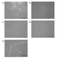
- the scale bar in each figure is 100 ⁇ m.
- the wave number in the Raman spectrum represents the center wave number and the half width of the E 2g peak derived from h-BN.
- the wave number in the Raman spectrum represents the center wave number and the half width of the E 2g peak derived from h-BN.
- the intensity of the E 2g peak derived from h-BN confirmed at 1365-1370 cm ⁇ 1 is shown.
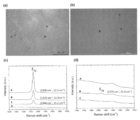
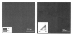
- Optical microscope image and atomic force microscope image of h-BN synthesized with Fe 0.3 -Ni 0.7 / spinel (100) (Ni 70%).
- A Optical microscope image (low magnification. Scale bar in the figure is 100 ⁇ m)
- Scale bar in the figure is 20 ⁇ m
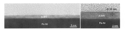
- (c) Atom Atomic force microscope image (scale bar in the figure is 10 ⁇ m). Transmission electron microscope image of h-BN synthesized with Fe 0.3 -Ni 0.7 / spinel (100) (Ni 70%). The scale bar of the left image is 5 nm and the scale bar of the right image is 1 nm.
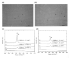
- (A) An atomic force microscope image of h-BN transferred from Fe 0.3 -Ni 0.7 / spinel (100) (Ni 70%) to a SiO 2 / Si substrate.
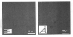
- Optical microscope image of h-BN synthesized using Fe 0.7 -Ni 0.3 / MgO (100) (Ni 30%) substrate and changing the cooling rate in CVD.
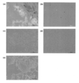
- the scale bar in each figure is 20 ⁇ m.
- the scale bar in each figure is 20 ⁇ m.
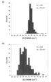
- (B) is a histogram showing the distribution of the half width of the E 2g peak.
- (A) 1100 ° C. (high magnification), (b) 1150 ° C. (high magnification), (c) 1100 ° C. (low magnification), (d) 1150 ° C. (low magnification).
- the scale bar in (a) and (b) is 20 ⁇ m, and the scale bar in (c) and (d) is 100 ⁇ m.
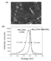
- (A) Atomic force microscope image of WS 2 atomic film synthesized by CVD method on h-BN synthesized using Fe 0.3 -Ni 0.7 / MgO (100) (Ni 70%) substrate.
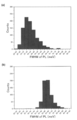
- (B) Fluorescence spectrum of WS 2 atomic film synthesized by CVD method on h-BN and SiO 2 / Si substrate synthesized using Fe 0.3 -Ni 0.7 / MgO (100) (Ni 70%) substrate. The histogram of the half value width of the fluorescence spectrum shown in FIG.24 (b).
- Patent Document 1 only specifically describes that a monoatomic film of graphene was produced using ethylene gas using the (111) plane of a single crystal Ni plate (substrate) as a template.
- Patent Document 2 specifically states that a desired graphene film was obtained by performing carbon doping by bringing toluene gas into contact with a single crystal or polycrystalline Ni substrate surface polished under a predetermined condition. It is only described in.
- Example 4 an example (Example 4) in which a boron nitride layer is formed between the substrate and the metal film is described, but the target boron nitride layer was actually obtained. Not shown.
- hexagonal boron nitride is composed of a regular arrangement of boron and nitrogen atoms, so the balance between boron and nitrogen atoms ( Atomic ratio) is an important factor.
- Atomic ratio Atomic ratio
- this inventor increases the generation amount of boron nitride by controlling the balance of a boron atom and a nitrogen atom on the surface of a metal thin film, and also improves the crystallinity and uniformity of the formed film. As a result of intensive studies, the present invention has been completed.
- the surface of the metal thin film has a thickness of 1 nm or more on the surface of the metal thin film by contacting the surface of the metal thin film with a source gas containing boron atoms, nitrogen atoms, or both boron atoms and nitrogen atoms.
- a source gas containing boron atoms, nitrogen atoms, or both boron atoms and nitrogen atoms.
- metal thin film means that it contains at least one element as a main component and is present in the raw material in a minute amount that does not affect the characteristics of the metal thin film or is unavoidable in the production process. It may contain impurities (inevitable impurities) that are mixed in automatically.
- the main component element of the metal thin film is preferably a metal having at least one of boron solubility and nitrogen solubility.
- the main component elements of the metal thin film include, but are not limited to, Fe, Ni, Co, Cu and Cr.
- the metal thin film contains at least one element selected from the group consisting of Fe, Ni, Co, Cu, and Cr as a main component element.
- the metal thin film contains two or more elements as main component elements.
- the metal thin film contains Ni and Fe, Co and Fe, or Cr and Fe as main component elements.
- the composition ratio of the main component elements in the metal thin film is not particularly limited, and can be appropriately adjusted according to boron solubility and nitrogen solubility. Specifically, for example, when the main component elements of the metal thin film are two (X and Y), these elements are considered in consideration of the solubility of boron and nitrogen in the element X and the solubility of boron and nitrogen in the element Y.
- the composition ratio (X: Y) can be adjusted. Thereby, the solubility of boron and nitrogen when the source gas contacts the surface of the metal thin film is appropriately controlled, and a hexagonal boron nitride thin film having a uniform thickness and high crystallinity can be formed. it can.
- the composition ratio of Ni and Fe is in the range of 1:99 to 99: 1, in the range of 5:95 to 95: 5, and in the range of 10:90 to The range can be 90:10, 20:80 to 80:20, 30:70 to 70:30, 40:60 to 60:40, or 50:50.
- the composition ratio of Ni and Fe can be in the range of 10:90 to 99: 1, and it is desirable to consider that the metal thin film is adjusted to contain 10% or more of Ni.
- the metal thin film is adjusted to contain 10% or more of Ni.
- the metal thin film may be a laminated film of metal films of two or more components, or may be a thin film of metal alloy of two or more components.
- the thin film of the metal alloy having two or more components may be a film formed on a predetermined substrate or a single metal foil having no substrate.
- the composition ratio of the main component elements can be adjusted, for example, by adjusting the film thickness of each metal film.
- the composition ratio of the main component elements is 50:50.
- the metal alloy may be a binary alloy mainly composed of two elements, or a ternary alloy mainly composed of three elements. Alternatively, it may be an alloy mainly composed of more than three elements.
- binary alloys include, but are not limited to, Ni—Fe, Co—Fe, and Cr—Fe.
- the composition ratio of the main component elements in the metal thin film is the same as the composition ratio in the metal alloy.
- the surface of the metal thin film preferably has a specific surface direction. Specifically, for example, the density of the crystal structure formed by the main component element contained in the metal thin film can be considered. In other words, even with the same metal species, by using a crystal plane controlled in a wider area, the solubility of boron and nitrogen when the source gas contacts the surface of the metal thin film is appropriately controlled and uniform. It is considered that a hexagonal boron nitride thin film having a large thickness and high crystallinity can be formed.
- the metal thin film is a laminated film of Ni and Fe metal films, or a Ni—Fe thin film of a binary alloy
- the surface thereof is a (111) plane of a face-centered cubic lattice, (100 ) Plane or (110) plane.
- a hexagonal boron nitride thin film is formed by a CVD method using a metal thin film containing two or more elements as a main component, the main component during the CVD reaction It is desirable to consider that relatively large crystal grains are present in the metal thin film after the CVD reaction because the element is transformed and the metal thin film is prevented from having a polycrystalline structure composed of small grains.
- the metal thin film when the metal thin film is a laminated film of Ni and Fe metal films, or a Ni—Fe thin film of a binary alloy, the metal thin film after the CVD reaction has a (111) face-centered cubic lattice. It is preferable to have a plane, (100 plane), or (110) plane.
- the metal thin film acts as a catalyst to generate boron nitride.
- the metal thin film is also referred to as “metal catalyst” depending on the context.
- the gas containing both a boron atom and a nitrogen atom can be used.
- it is preferably considered to contain boron and nitrogen in a molar ratio of 1: 1, but is not limited thereto.
- Specific examples include vaporized gases such as borazine (B 3 N 3 H 6 ), ammonia borane (BH 3 NH 3 ), and 2,4,6-trichloroborazine (B 3 Cl 3 H 3 N 3 ). It is done.
- the gas containing a boron atom and the gas containing a nitrogen atom can also be used separately.
- a molecular gas containing boron gas and nitrogen, a molecular gas containing boron and a nitrogen gas, or a molecular gas containing boron and a molecular gas containing nitrogen can be used in combination.
- the molecule containing boron include diborane (B 2 H 6 ), trichloroborane (BCl 3 ), and trifluoroborane (BF 3 ).
- the molecule containing nitrogen include ammonia (NH 3 ) and nitrogen molecule (N 2 ).
- source gas it may be used individually by 1 type and may use 2 or more types together.
- a gas containing both boron atoms and nitrogen atoms may be used alone, or two or more gases containing both boron atoms and nitrogen atoms may be used in combination.
- the selection and combination of such source gases can be appropriately adjusted according to the properties of the metal catalyst used (for example, boron solubility, nitrogen solubility, etc.), the required thickness of the hexagonal boron nitride thin film, and the like.
- the hexagonal boron nitride thin film manufactured according to the exemplary embodiment of the present invention is formed by, for example, a chemical vapor deposition (CVD) method.
- CVD chemical vapor deposition
- a metal thin film that serves as a catalyst for boron nitride formation is formed on a substrate (eg, a single crystal substrate).
- a substrate eg, a single crystal substrate
- a single metal foil having no substrate is used as the metal catalyst.
- the single crystal substrate is not particularly limited.
- a metal oxide single crystal such as an alkaline earth metal, a transition metal, or a rare earth metal can be used.
- MgO manganesium oxide
- ⁇ -Al 2 O 3 sinite
- MgAl 2 O 4 spinel
- SiO 2 crystal
- LaAlO 3 laAlO 3
- TiO 2 titanium dioxide
- Mica for example, KMg 3 AlSi 3 O 10 F 2 ) and the like.
- the size of the single crystal substrate is not particularly limited, but is preferably 1 to 1,000,000 mm 2 and preferably 100 to 20,000 mm 2 in view of obtaining a good hexagonal boron nitride thin film and other conditions.
- the size of the metal foil is not particularly limited, and can be appropriately adjusted according to the use of the hexagonal boron nitride thin film.
- sputtering is performed on the single crystal substrate. Conditions such as the heat treatment temperature of the substrate during sputtering are appropriately adjusted according to the type of metal used. Further, as a film forming method other than sputtering, for example, vapor deposition by resistance heating, vapor deposition by an electron beam, plating film formation, or the like is possible.
- the thickness of the metal thin film is preferably 0.005 to 1000 ⁇ m, more preferably 0.1 to 100 ⁇ m.
- the metal thin film contains at least one element selected from the group consisting of Fe, Ni, Co, Cu and Cr as a main component element. In a more preferred embodiment, the metal thin film contains two or more elements as main component elements.
- the metal thin film can be a laminated film of two or more component metal films.
- the composition ratio of the main component elements of the metal thin film can be controlled by, for example, the film thickness of each element.
- one metal (X) film is laminated by 300 ⁇ m, and the other metal (Y) film is laminated by 700 ⁇ m, for a total of 1 ⁇ m.
- the metal thin film can be a thin film of a metal alloy of two or more components.
- a metal thin film having a predetermined composition ratio can be produced using an alloy target having a composition having two or more components.
- the composition ratio of the main component elements is the same as that in the metal alloy.
- the crystal structure of the surface of the metal thin film is not particularly limited, but the solubility of boron and nitrogen in the main component elements contained in the metal thin film can be considered.
- the crystal structure of the surface of the metal thin film has a specific plane direction, boron and nitrogen are efficiently dissolved in the metal, thereby increasing the amount of precipitation during cooling and uniform at 1 nm or more.
- a hexagonal boron nitride thin film having a thickness can be formed. It is understood that the composition ratio of the main component elements, the size of the crystal grains of the metal, and the like can be the main factors regarding the solid solution amounts of boron and nitrogen in the metal.
- Boron nitride is produced by bringing a raw material gas into contact with the surface of such a metal thin film, and a hexagonal boron nitride thin film is grown.
- the source gas is preferably supplied at a constant pressure into a substrate in which a metal thin film is formed on the surface of a single crystal substrate or a chamber in which a metal foil is disposed.
- an inert gas such as helium or argon or hydrogen gas may be supplied into the chamber.
- the pressure of the source gas in the chamber is preferably from 10 5 to 10 ⁇ 5 Pa, more preferably from 10 5 to 10 ⁇ 3 Pa, under atmospheric pressure or reduced pressure.
- the heat treatment temperature is preferably from 300 to 1500 ° C., more preferably from 400 to 1200 ° C., and even more preferably from 500 to 1150 ° C., from the viewpoint of forming a boron nitride and obtaining a good hexagonal boron nitride thin film.
- the heat treatment time is preferably 1 to 300 minutes, more preferably 10 to 60 minutes.
- the heating means for the heat treatment is not particularly limited, but for example, heat radiation, induction heating, laser, infrared, microwave, plasma, ultraviolet, surface plasmon heating, or the like can be used.
- the metal thin film surface of the catalyst is reduced by hydrogen annealing at a temperature lower than the CVD synthesis temperature, thereby improving the crystallinity of the metal thin film surface even at a high temperature during the CVD synthesis. can do. Specifically, by performing hydrogen annealing at a low temperature, the aggregation of the metal catalyst and the generation of pits on the surface of the metal thin film are suppressed, thereby enabling the growth of a hexagonal boron nitride thin film having a large area. It is also effective to perform hydrogen annealing at the CVD temperature after hydrogen annealing at this low temperature.
- This hydrogen annealing can be performed immediately before CVD synthesis by placing a sample in a chamber where CVD is performed.
- the temperature of the hydrogen annealing can be performed, for example, at 400 to 600 ° C. or 1000 to 1200 ° C.
- the longer the annealing time the better the crystallinity of the metal catalyst and the quality of the boron nitride synthesized.
- the gas supply during the hydrogen annealing is set according to the volume of the chamber, but can be performed, for example, while flowing 10 to 10,000 sccm of hydrogen together with an inert gas per liter of the chamber volume.
- cooling is performed.
- boron and nitrogen dissolved in the metal catalyst are deposited on the surface of the metal thin film to generate boron nitride, and a hexagonal boron nitride thin film is formed on the surface of the metal thin film.
- the cooling rate is not particularly limited, it is thought that by cooling at a slower rate, boron and nitrogen precipitate more evenly to generate boron nitride, and the uniformity of the formed hexagonal boron nitride thin film is further improved. It is done.
- the cooling rate can be 0.01 to 50 ° C./min, preferably 0.1 to 10 ° C./min, more preferably 0.1 to 5.0 ° C./min, further 0.1 to 1.0 ° C./min. More preferred. Further, the cooling rate may be a constant rate, or a plurality of cooling rate conditions may be combined. For example, after CVD synthesis, from the CVD synthesis temperature to the middle of the cooling process (for example, until reaching 700 ° C), the cooling rate is 0.1 to 1.0 ° C / min, and then adjusted to any cooling rate selected from the above cooling rate conditions can do. In addition, cooling is performed, for example, flowing hydrogen gas.
- a part or all of the inert gas or hydrogen gas is replaced with a source gas containing a boron atom or a nitrogen atom (second source material). Gas).
- the solid solubility of boron and nitrogen in the metal catalyst is assumed to vary depending on the metal species used, in addition to adjusting the type and supply amount of the source gas, it contains boron atoms or nitrogen atoms.
- the gas as the second raw material gas when boron and nitrogen solid-dissolved in the metal catalyst are deposited during cooling, a deficient boron atom or nitrogen atom is supplemented, and boron atoms are formed on the surface of the metal thin film.
- the balance of nitrogen atoms closer to 1: 1 1, the amount of boron nitride produced is further increased, and a hexagonal boron nitride thin film having a constant thickness of 1 nm or more can be formed.
- a hexagonal boron nitride thin film having a uniform thickness and high crystallinity can be obtained because the above various production conditions are related to each other. That is, when boron nitride is generated by the CVD method as exemplified, factors such as the metal species related to the metal catalyst, crystal plane, crystal grain size, etc., factors such as the type and composition of the gas related to the source gas, and gas supply related to the CVD (Including gas supply as the second source gas), temperature profile and other factors are related to each other, so it has a large area, a uniform thickness of 1 nm or more, and a low grain boundary. A hexagonal boron nitride thin film can be obtained.
- the hexagonal boron nitride thin film of the present invention produced by the production method exemplified above is a hexagonal boron nitride thin film having a large area with a uniform thickness and high crystallinity.
- magnesium oxide (MgO), sapphire ( ⁇ -Al 2 O 3 ), spinel (MgAl 2 O 4 ), quartz (SiO 2 ), mica, etc. are relatively inexpensive and large area
- a large-area hexagonal boron nitride thin film is formed on the metal thin film formed on the single crystal substrate.
- a large-area hexagonal boron nitride thin film can be formed on a single metal foil using the CVD method described above.
- the hexagonal boron nitride thin film of the present invention is a boron nitride thin film having a thickness of 1 nm or more, that is, consisting of three or more atomic layers.
- a hexagonal boron nitride thin film having a thickness of 1 nm or more and 50 nm or less can be obtained.
- the thickness of the hexagonal boron nitride thin film can be estimated by using, for example, a thin piece of hexagonal boron nitride peeled from a single crystal.
- the height of a hexagonal boron nitride flake peeled from a single crystal or transferred from a metal catalyst on a silicon substrate having an oxide film for example, a Si substrate with 300 nm SiO 2
- the thickness of the hexagonal boron nitride thin film can be estimated by measuring with an atomic force microscope and measuring the optical contrast with an optical microscope.
- the thickness of the hexagonal boron nitride thin film can be estimated by analyzing the cross section of the produced thin film with an atomic force microscope or a transmission electron microscope.
- the hexagonal boron nitride thin film of the present invention is excellent in thickness uniformity.
- the thickness uniformity of the hexagonal boron nitride thin film is, for example, exfoliated from a single crystal or transferred from a metal catalyst to a silicon substrate having an oxide film (for example, a Si substrate with 300 nm of SiO 2 ).
- the hexagonal boron nitride thin film of the present invention has a variation coefficient of 5% or less of the intensity distribution of the G component of an RGB image obtained by an optical microscope on a silicon substrate having an oxide film. It is.
- the intensity distribution of the G component of the RGB image obtained by an optical microscope shows a unimodality on a silicon substrate having an oxide film.
- the “variation coefficient” means the degree of dispersion of the values. Since the intensity of the G component (and its average) varies depending on the preparation method of the observation sample, the observation conditions, and the like, in the present invention, the coefficient of variation obtained by dividing the standard deviation by the average is used as an index. The smaller the value of the coefficient of variation, the closer the intensity distribution of the G component is to a single color, which means that the hexagonal boron nitride thin film has a more uniform layer structure. “Monomodal” means that the hexagonal boron nitride thin film covers the silicon substrate within the field of view.
- the intensity distribution of the G component is “bimodal”.
- the hexagonal boron nitride thin film has a non-uniform layer structure (number of layers)
- the intensity distribution of the G component is widely dispersed and becomes “multimodal”.
- the peak due to the silicon oxide film on the surface of the silicon substrate can be generated depending on the accuracy of the transfer method, etc.
- hexagonal boron nitride thin film is excellent in the uniformity of the layer structure (number of layers) as long as a sharp peak due to hexagonal boron nitride is obtained. Note that you get.
- the hexagonal boron nitride thin film of the present invention has high crystallinity.
- the crystallinity of the hexagonal boron nitride thin film can be confirmed, for example, by measuring the Raman spectrum and measuring the position and half width of the E 2g peak derived from hexagonal boron nitride.
- a plurality of (for example, at least 50 or more) measurement positions are selected from a microscope image obtained by observing a hexagonal boron nitride thin film at a predetermined magnification with an optical microscope, and obtained at each measurement position.
- the hexagonal boron nitride thin film of the present invention has an average value of the full width at half maximum (full width at half maximum: FWHM) of the E 2g peak obtained by Raman spectrum of 20 cm ⁇ 1 or less.
- the hexagonal boron nitride thin film of the present invention has an average value of 9 to 20 cm ⁇ 1 of the half width (full width at half maximum: FWHM) of the E 2g peak obtained by Raman spectrum.
- Example 1 An MgO substrate having a (100) plane was used as the single crystal substrate. This substrate is mounted in a chamber of an RF magnetron sputtering apparatus, and Fe metal and / or Ni metal or both are formed on the surface of the substrate by sputtering while the substrate is heated (Ar atmosphere, the vacuum degree is 0.6 Pa as standard) ).
- the substrate was 500-400 ° C. when using Fe and 600-500 ° C. when using Ni.
- the temperature of the substrate may be room temperature (about 25 ° C.) or any other temperature when using Fe and using Ni.
- the substrates on which these metal catalysts are deposited are referred to as Fe / MgO (100), Ni / MgO (100), and Fe—Ni laminated / MgO (100), respectively.
- the substrate was cut into an appropriate size, for example, 5 mm square or 10 mm square as necessary, and the h-BN thin film was synthesized by the CVD method according to the following procedure. .
- a horizontal tubular furnace Using a horizontal tubular furnace, a single crystal substrate having a catalytic metal film formed at the center of a quartz tube attached to the tubular furnace was placed using a quartz boat.
- Fe foil manufactured by Niraco, thickness 20 ⁇ m
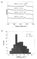
- CVD synthesis was performed using the temperature profile shown in FIG.
- the entire quartz tube was evacuated by a rotary pump. Thereafter, hydrogen gas was flowed at 10 sccm to 40-50 Pa. While flowing the same amount of hydrogen gas, the temperature was raised to 1100 ° C. over 60 minutes as shown in FIG. 1, and the temperature was maintained for 60 minutes. As a result, the crystallinity of the sputtered metal catalyst was increased and the smoothness of the surface was improved. At the same time, the natural oxide film on the metal surface is removed by hydrogen gas.
- Borazine (B 3 N 3 H 6 ) was used as a raw material for boron and nitrogen. Liquid borazine was placed in a bottle with a hydrogen atmosphere of 0.12 to 0.13 MPa, and the bottle was cooled to -10 ° C. From the bottle, 0.27 sccm of hydrogen gas containing borazine vapor was mixed with 10 sccm of hydrogen gas in the main line and introduced into the tubular furnace. This reaction was carried out for 30 minutes.
- the hydrogen gas containing the borazine gas was shut off, and the cooling rate was controlled at 1 ° C / min to 700 ° C while flowing only 10 ⁇ ⁇ sccm of the main line hydrogen gas. After reaching 700 ° C, the tube furnace was turned off and cooled to room temperature.
- the substrate was taken out.
- the h-BN formed on the metal film was transferred onto a SiO 2 / Si substrate.
- the amount of h-BN produced and the thickness distribution can be easily observed with an optical microscope.
- Raman spectroscopy the peak obtained from h-BN becomes strong, and more accurate evaluation is possible.
- transfer was performed by the following method.
- a polymethyl methacrylate (PMMA) solution was spin-coated on the surface of the synthesized metal thin film, and a PMMA film for protecting h-BN was formed by baking at 115 ° C. for 20 minutes.
- a thermal tape (Revalpha manufactured by Nitto Denko Corporation) was pasted on PMMA.
- the substrate was immersed in a mixed solution of FeCl 3 aqueous solution and hydrochloric acid, and after the catalyst was etched sufficiently, h-BN floated on the solution surface together with the thermal tape and PMMA, and then picked up with tweezers.
- the h-BN after being transferred to the SiO 2 / Si substrate was analyzed with an optical microscope.
- Nikon ECLIPSE ME600 was used as the optical microscope, and Nikon DS-Fi1 was used as the CCD camera.
- 2 and 3 show micrographs. 2 is a high magnification image and FIG. 3 is a low magnification image.
- the thickness of h-BN shown in FIG. 2 (d) was estimated using h-BN flakes peeled from a single crystal.
- the height of the peeled h-BN flakes was determined with an atomic force microscope (Bruker, Nanoscope IV), and the optical contrast was measured with an optical microscope.
- the thickness of h-BN shown in FIG. 2 (d) was estimated to be about 3-10 nm.
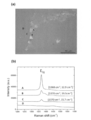
- FIG. 4A to 4C are measurement results of optical microscope images and Raman spectra of h-BN transferred to a SiO 2 / Si substrate.
- Nanofinder30 manufactured by Tokyo Instruments was used, the excitation wavelength was 532 nm, and the spot size was about 0.6 ⁇ m.
- FIG. 4A is an optical microscope image and a Raman spectrum of h-BN obtained with Fe / MgO (100) and Ni / MgO (100).
- FIG. 4A is an optical microscope image and a Raman spectrum of h-BN obtained with Fe / MgO (100) and Ni / MgO (100).
- Fig. 4B shows optical microscope images and Raman spectra of h-
- FIGS. 4A to 4C shows an optical microscope image and a Raman spectrum of h-BN transferred from the Fe foil to the SiO 2 / Si substrate.
- the positions where the Raman spectra were measured were shown.
- the peak position and the half value width (FWHM) were described in the Raman spectrum.
- Fe 0.3 -Ni 0.7 / MgO (100) (Ni 70%) gives a more uniform peak intensity between the measurement positions A to C. It was. This indicates that the latter h-BN film is superior in uniformity.
- the half width of the E 2g peak in FIGS. 4B (c) and 4 (d) is within the range of 13 to 20 cm ⁇ 1 , reflecting the high crystallinity.
- an E 2g peak derived from h-BN was confirmed, but the uniformity of the peak intensity was not observed between the measurement positions A to C. From the half-width value of the E 2g peak, It can be seen that the crystallinity also varies.
- the Fe thin film of the Fe / MgO (100) substrate shown in FIG. 7 (a) is made of grains having small and various orientations. It is known that when Fe is heated, it undergoes a phase transition (transformation) from a body-centered cubic structure (bcc structure, ⁇ iron) to a face-centered cubic structure (fcc structure, ⁇ iron) at 910 ° C.
- Ni metal of Ni / MgO (100) shows a uniform fcc (100) surface. This indicates that Ni has a stable fcc structure from room temperature to high temperature, and the Ni (100) thin film epitaxially deposited on MgO (100) is maintained even during high-temperature CVD.
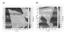
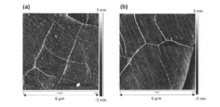
- FIG. 8 shows the result of observing the surface of the h-BN transfer film with an atomic force microscope (AFM).
- the h-BN produced on Fe / MgO (100) is relatively smooth, but the warpage of the thin film grain is remarkable at the edge (FIG. 8 (a)). Little formation of h-BN occurred on Ni / MgO (100), and only a small amount of flakes were observed (Fig. 8 (b)).
- the h-BN transferred from Fe 0.7 -Ni 0.3 / MgO (100) (Ni 30%) had a smooth surface but had a plurality of particles (FIG. 8 (c)).
- the h-BN grain thickness was estimated to be about 4.5 nm from the analysis of the height profile of the atomic force microscope (FIG. 8 (e)). Further, in FIG. 8 (d), it can be seen that the adjacent grains are quite close in height.
- Example of using this Fe 0.3 -Ni 0.7 / spinel (100) (Ni 70%) substrate, except that 25% of nitrogen gas was mixed with hydrogen gas used for supplying and cooling the borazine vaporized raw material
- the h-BN thin film was synthesized by the CVD method under the same conditions as in Example 1, and the generated h-BN was transferred onto the SiO 2 / Si substrate in the same manner as in Example 1.
- FIGS. 10A to 10C are an optical microscope image (low magnification and high magnification) and an atomic force microscope image of the synthesized h-BN, respectively. From these microscopic images, it was confirmed that a very uniform h-BN thin film having a thickness of about 3 nm was obtained.
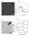
- FIG. 12 shows the measurement results of the atomic force microscope image and the Raman spectrum of h-BN transferred to the SiO 2 / Si substrate.
- FIG. 12 (c) is an intensity mapping of the E 2g peak of the Raman spectrum in the same area as FIG. 12 (a), and FIG. 12 (d) is a Raman spectrum at the position indicated by the number in FIG. 12 (c). is there. From the atomic force microscope image of FIG.
- the multilayer h-BN has a very uniform film thickness. Also, from FIG. 12 (b), the thickness of this h-BN was about 2.5 nm. Further, the Raman mapping images of FIGS. 12 (c) and 12 (d) also show that h-BN having uniform E 2g peak intensity and excellent layer number uniformity can be synthesized and transferred. .
- Example 1 A Ni / spinel (100) was prepared by sputtering Ni metal on the substrate surface by the same procedure as in Example 1 except that a spinel substrate having a (100) plane was used as the single crystal substrate.
- Example 2 Using this Ni / spinel (100) substrate, the CVD method was used under the same conditions as in Example 1 except that 50% of nitrogen gas was mixed with hydrogen gas used for supplying and cooling the borazine vaporized raw material. A -BN thin film was synthesized, and the generated h-BN was transferred onto a SiO 2 / Si substrate in the same manner as in Example 1.
- Example 2-2> Except that a spinel substrate having a (100) plane was used as a single crystal substrate, Fe metal and Ni metal were formed on the substrate surface by sputtering in the same procedure as in Example 1, and Fe 0.7 -Ni 0.3 / spinel. (100) (Ni 30%) (Ni film 300 nm, Fe film 700 nm) was produced.
- Example of using this Fe 0.7 -Ni 0.3 / spinel (100) (Ni 30%) substrate, except that 25% of nitrogen gas was mixed with hydrogen gas used for supplying and cooling the borazine vaporized raw material
- the h-BN thin film was synthesized by the CVD method under the same conditions as in Example 1, and the generated h-BN was transferred onto the SiO 2 / Si substrate in the same manner as in Example 1.
- the h-BN after being transferred to the SiO 2 / Si substrate was analyzed with an optical microscope. As shown in FIG. 15, a microscopic image with a substantially uniform optical contrast was obtained, and it was confirmed that h-BN with high uniformity was generated.
- FIG. 17A is a diagram showing the intensity distribution of the G component extracted from the RGB image
- FIG. 17B is a G component image of the RGB image obtained by the optical microscope.
- FIG. 17A shows the mean (MEAN), standard deviation (SD), and coefficient of variation (CV (%)) of the G component intensity.
- the peak observed near G values 170 to 185 is a peak derived from the oxide (SiO 2 ) of the Si substrate.
- Example 5-1 Instead of the Fe-Ni laminated film (metal catalyst) formed on the single crystal substrate used in Example 1, synthesis of an h-BN thin film by the CVD method using three types of metal foils having the following compositions: Went.
- an h-BN thin film was synthesized by the CVD method under the same conditions as in Example 1 except that the cooling rate in CVD was 5 ° C./min.
- the results are shown in FIG. From the optical microscopic images of FIGS. 19 (a) to 19 (c), it was confirmed that h-BN was generated in any metal foil.
- an h-BN thin film was synthesized by the CVD method under the same conditions as in Example 1 except that the cooling rate in CVD was 1 ° C./min.
- the results are shown in FIG. From the optical microscope images of FIGS. 20 (a) to 20 (c), it was confirmed that h-BN was formed in any metal foil.
- the cooling rate was 5 ° C./min (FIG. 19)
- the generation of h-BN was broadened as a whole.
- Super Invar has a multilayer h-BN film covering the entire surface of the metal foil. This is one of the factors that the cooling rate in CVD affects the amount of h-BN produced. When the cooling rate is slowed down, the amount of h-BN produced increases, resulting in the formation of a more uniform and widened h-BN thin film. Suggests that it leads to
- the cooling rate from the synthesis temperature is 5 ° C / min, 1
- the h-BN thin films with better uniformity were observed as the temperature decreased to °C / min, 0.5 °C / min, and 0.25 °C / min.
- the cooling rate in the temperature range close to the synthesis temperature in the initial stage of the cooling process may lead to an increase in the amount of h-BN produced and the formation of a more uniform and widened h-BN thin film.
- FIG. 21 (d) shows that the homogeneity of h-BN is greatly improved and high-quality h-BN can be synthesized.
- FIG. 22 shows the measurement result of the Raman spectrum of h-BN synthesized under the condition (ii).
- an E 2g peak derived from h-BN is confirmed at 1368-1369 cm ⁇ 1, and it can be seen that the crystallinity is good from the value of the half width.
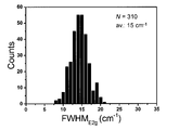
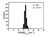
- 150 spots were randomly selected from the 20 ⁇ m square area of h-BN, and the intensity and half-width (FWHM) of the E 2g peak derived from h-BN were measured.
- the average value of the half width of the E 2g peak was 13 cm ⁇ 1 , and it was confirmed to be h-BN having high crystallinity.
- Example 5-2> Using the super invar used in Example 5-1, the temperature profile for CVD synthesis was changed to synthesize an h-BN thin film. Specifically, as shown in FIG. 1, the temperature is raised to 1100 ° C. over 60 minutes, held at that temperature for 40 minutes, and then heated to 1150 ° C. over 20 minutes. The CVD reaction was performed for 30 minutes according to the procedure described above. Thereafter, the tube was cooled to 700 ° C. at a rate of 5 ° C./min. After reaching 700 ° C., the tubular furnace was turned off and cooled to room temperature.
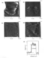
- FIG. 23 is an optical microscope image of h-BN after being transferred to the SiO 2 / Si substrate.
- FIG. 23 (a) and FIG. 23 (c) are a high-magnification image and a low-magnification image of h-BN synthesized under the conditions of (i) of Example 5-1, and FIGS. 23 (b) and (d) These are a high-magnification image and a low-magnification image of h-BN synthesized in this example.
- 23 (a) to 23 (d) the h-BN synthesized in this example was compared with the h-BN produced under the condition (i) in Example 5-1 and the grain size of h-BN.
- h-BN synthesized in the present example is the condition of (i) of Example 5-1 even in a state where it was generated on the metal foil after the completion of the CVD reaction before transfer to the SiO 2 / Si substrate. Compared with h-BN synthesized in step 1, non-uniform precipitation of h-BN was observed in the optical microscope image, confirming that the h-BN film had better uniformity. .
- FIG. 24 (a) is an atomic force microscope image of WS 2 grown on h-BN. It can be seen from the triangular shape that WS 2 is thin and grows as a small single crystal.
- FIG. 24B shows the result of the fluorescence spectrum. It can be seen that the peak intensity of WS 2 grown on h-BN is strong and 46 times stronger than WS 2 grown on SiO 2 . It can also be seen that the line width of WS 2 PL on h-BN is very narrow from 72 meV to 24 meV.
- FIG. 25 is a half-width histogram of the fluorescence spectrum shown in FIG. From the histograms shown in FIGS.
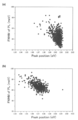
- FIG. 26 is a scatter diagram obtained by adding the peak position information in the fluorescence spectrum of FIG. 24B to the information of the histogram of FIG. In the scatter diagrams shown in FIGS.
- Example 8 the single-layer graphene formed by CVD was transferred onto h-BN and SiO 2 / Si synthesized using a super invar of metal foil, and the graphene characteristics were analyzed by Raman spectrum.
- Single-layer graphene is obtained by depositing Cu (111) on a sapphire substrate by CVD, spin-coating a polymethyl methacrylate (PMMA) solution on the surface, and removing Cu by etching. Transferred on BN or SiO 2 / Si.
- PMMA polymethyl methacrylate
- the half-value width (26 cm -1 ) of the 2D band of graphene on h-BN is the graphene (lower spectrum) on SiO 2 / Si. It can be seen that h-BN significantly reduces the influence from SiO 2 , which is narrower than the half-value width (34 cm ⁇ 1 ).
- the intensity ratio (I 2D / I G ) between the 2D band and the G band between graphene on h-BN and graphene on SiO 2 / Si the former is 3.6 and the latter is 2.4. Therefore, it can be understood that graphene on h-BN is in an ideal state to exhibit its characteristics.
- the half-width (26 cm -1 ) of the 2D band of graphene on h-BN is about the same as that reported so far for graphene on h-BN exfoliated from the bulk single crystal. It shows that the h-BN of the invention has a shielding effect comparable to that caused by peeling.
- FIG. 28 is a histogram showing the distribution of the half-width (FWHM) of the 2D band at a plurality of measurement points for graphene on h-BN and graphene on SiO 2 / Si.
- FWHM half-width
- the hexagonal boron nitride thin film according to the present invention has the characteristics of a large area with a uniform thickness and high crystallinity, it can be used for various electronic devices including semiconductor devices.
Landscapes
- Chemical & Material Sciences (AREA)
- Engineering & Computer Science (AREA)
- Organic Chemistry (AREA)
- Materials Engineering (AREA)
- Metallurgy (AREA)
- Chemical Kinetics & Catalysis (AREA)
- Mechanical Engineering (AREA)
- General Chemical & Material Sciences (AREA)
- Inorganic Chemistry (AREA)
- Ceramic Engineering (AREA)
- Manufacturing & Machinery (AREA)
- Structural Engineering (AREA)
- Crystallography & Structural Chemistry (AREA)
- Chemical Vapour Deposition (AREA)
- Thin Film Transistor (AREA)
- Compositions Of Oxide Ceramics (AREA)
- Crystals, And After-Treatments Of Crystals (AREA)
Abstract
Description
好ましい態様では、この六方晶窒化ホウ素薄膜は、光学顕微鏡によって得られるRGB画像のG成分の強度分布の変動係数が5%以下である。
また、好ましい態様では、この六方晶窒化ホウ素薄膜は、前記G成分の強度分布が単峰性を示す。
また、好ましい態様では、この六方晶窒化ホウ素薄膜は、厚さが1nm以上、50nm以下である。
また、好ましい態様では、この六方晶窒化ホウ素薄膜は、3層以上の層からなる。
「単峰性」とは、視野内において六方晶窒化ホウ素薄膜がシリコン基板を覆っていることを意味する。視野内においてシリコン基板の露出が確認される場合には、シリコン基板表面の酸化物に起因するピークが生じるため、G成分の強度分布は「二峰性」となる。また、六方晶窒化ホウ素薄膜の層構造(層数)が不均一である場合には、G成分の強度分布は幅広く分散し、「多峰性」となる。ここで、G成分の強度分布が二峰性を示す場合であっても、シリコン基板表面のシリコン酸化膜に起因するピークは、転写手法の精度等に依存して生じ得るため、六方晶窒化ホウ素薄膜自体の品質を直接的に示すものではなく、六方晶窒化ホウ素に起因する鋭いピークが得られる限りにおいて、六方晶窒化ホウ素薄膜は層構造(層数)の均一性に優れていると理解され得る点に留意されたい。
単結晶基板として(100)面をもつMgO基板を用いた。この基板をRFマグネトロンスパッタリング装置のチャンバー内に装着して、基板を加熱した状態で基板表面にFe金属またはNi金属、あるいはその両方をスパッタリングにより成膜した(Ar雰囲気、真空度は0.6 Paが標準)。
水平型の管状炉を用い、管状炉に取り付けた石英管の中央部に触媒金属を成膜した単結晶基板を、石英ボートを用いて設置した。
単結晶基板として(100)面をもつスピネル基板を用いたこと以外は実施例1と同様の手順で、基板表面にFe金属およびNi金属をスパッタリングにより成膜して、Fe0.3-Ni0.7/スピネル(100) (Ni=70%)(Ni膜700 nm、Fe膜300 nm)を作製した。
図12(a)の原子間力顕微鏡像から、この多層h-BNは膜厚が極めて均一であることが確認できる。また、図12(b)より、このh-BNの厚さは約2.5 nmであった。さらに、図12(c)、(d)のラマンマッピング像からも、E2gピークの強度が均一であり、層数均一性に優れたh-BNが合成・転写できていることを示している。
単結晶基板として(100)面をもつスピネル基板を用いたこと以外は実施例1と同様の手順で、基板表面にNi金属をスパッタリングにより成膜して、Ni/スピネル(100)を作製した。
単結晶基板として(100)面をもつスピネル基板を用いたこと以外は実施例1と同様の手順で、基板表面にFe金属およびNi金属をスパッタリングにより成膜して、Fe0.7-Ni0.3/スピネル(100) (Ni=30%)(Ni膜300 nm、Fe膜700 nm)を作製した。
次に、Feホイル、Fe/MgO(100)、Fe0.3-Ni0.7/MgO(100) (Ni=70%)で得られたSiO2/Si基板に転写した後のh-BN(以上、実施例1)、およびFe0.3-Ni0.7/スピネル(100) (Ni=70%)で得られたSiO2/Si基板に転写した後のh-BN(実施例2-1)について、光学顕微鏡によって得たRGB画像のG成分の分布を測定した。図17(a)は、RGB画像から抽出したG成分の強度分布を示す図であり、図17(b)は、光学顕微鏡によって得られたRGB画像のG成分像である。本実施例では、各々のRGB画像から約30,000ポイントを任意に選択してG成分の値を測定した。図17(a)には、G成分強度の平均(MEAN)、標準偏差(SD)、変動係数(CV(%))を記載した。なお、図17(a)において、G値170~185付近に見られるピークは、Si基板の酸化物(SiO2)に由来するピークである。
金属触媒を製膜する単結晶基板の結晶面とh-BN生成との関係を調べるため、(111)面をもつMgO基板(MgO(111))、および(111)面をもつスピネル基板(スピネル(111))を用いたこと以外は実施例1と同様の手順で、基板表面にFe金属およびNi金属をスパッタリングにより成膜して、Fe0.3-Ni0.7/MgO(111) (Ni=70%)、Fe0.3-Ni0.7/スピネル(111) (Ni=70%)を作製した。
次に、実施例1で用いたFe0.7-Ni0.3/MgO(100) (Ni=30%)を用い、CVDでの冷却速度を5℃/min、2.5℃/min、1℃/minと変えて、冷却速度とh-BN生成量との関係を調べた。結果を図18に示す。冷却速度が5℃/min(図18(a))の場合と比較して、2.5℃/min(図18(b))と1℃/min(図18(c))ではより広がったh-BN薄膜が観察された。この両者では、1℃/minの方がh-BN薄膜の生成量はより多かった。これらの結果は、CVDでの冷却速度がh-BN生成量に大きな影響を与える要因のひとつであり、冷却速度が遅いほど、より均一で広がったh-BN薄膜の生成につながることを示唆している。
実施例1で用いた単結晶基板上に製膜したFe-Ni積層膜(金属触媒)に代えて、以下の組成を有する3種類の金属箔を用いて、CVD法によるh-BN薄膜の合成を行った。
(1)スーパーインバー(Feリッチ)
Fe:Balance(63~65 %)
Ni:31 %
Co:4~6 %
(2)42インバー(Feリッチ)
Fe:Balance(56~57 %)
Ni:約42 %
Co:1~2 %
(3)78パーマロイ(Niリッチ)
Fe:Balance(約16~17 %)
Ni:約78 %
Co:1~2 %
Mo:4 %
図19(a)~(c)の光学顕微鏡像より、いずれの金属箔でもh-BNの生成が確認され、スーパーインバー(図19(a))、42インバー(図19(b))、78パーマロイ(図19(c))の順に、h-BNの生成量が少なくなっており、h-BNの広がりも抑制されている傾向が見られた。
図20(a)~(c)の光学顕微鏡像より、いずれの金属箔でもh-BNの生成が確認された。一方、冷却速度が5℃/minの場合(図19)と比較して、全体的にh-BNの生成の広がりが見られた。特に、スーパーインバーでは金属箔全面に多層h-BN膜が被覆するようになっている。このことは、CVDでの冷却速度がh-BN生成量に影響を与える要因のひとつであり、冷却速度を遅くするとh-BN生成量が増加し、より均一で広がったh-BN薄膜の生成につながることを示唆している。
(i) 5℃/minで700℃まで冷却する
(ii) 1℃/minで700℃まで冷却する
(iii) 0.5℃/minで900℃まで冷却し、5℃/minで700℃まで冷却する
(iv) 0.25℃で1050℃まで冷却し、5℃/minで700℃まで冷却する
図21(a)~(d)の光学顕微鏡像より、合成温度からの冷却速度を5℃/min、1℃/min、0.5℃/min、0.25℃/minと遅くなるにつれてより均一性に優れたh-BN薄膜が観察された。このことは、冷却工程の初期段階における合成温度に近い温度領域での冷却速度が、h-BN生成量の増加、およびより均一で広がったh-BN薄膜の生成につながる可能性を示唆している。特に図21(d)は、h-BNの均一性が非常に向上し、高品質のh-BNが合成できたことを示している。
実施例5-1で用いたスーパーインバーを用いて、CVD合成の温度プロファイルを変更し、h-BN薄膜の合成を行った。具体的には、図1に示すように1100℃まで60分かけて昇温し、その温度で40分保持した後、1150℃まで20分かけて昇温し、その温度で実施例1と同様の手順でCVD反応を30分間行った。その後、5℃/minの速度で700℃まで冷却し、700℃に達した後は管状炉の電源を切り、室温まで冷却した。
ところで、図2および図3に関する上記の結果は、ホウ素と窒素がFe中に固溶し、それらが冷却時に析出する際にh-BNが生成され、基板上で薄膜を形成することによるものであると解釈できる。すなわち、Feへのホウ素と窒素の固溶度は十分高いため、比較的厚いh-BN薄膜が形成される。それに対し、Niは窒素の固溶量が少ないため、比較的薄くて密度の低いh-BN薄膜が形成されるものと解釈できる。
次に、CVD法により合成されたh-BN薄膜が、他の原子膜材料の絶縁材料として有効であることを実証するため、Fe0.3-Ni0.7/MgO(100) (Ni=70%)基板を用いて合成したh-BN上とSiO2/Si基板上にCVD法によってWS2原子膜を合成し、その蛍光スペクトルを評価した。なお、WS2原子膜は、WO3と硫黄粉末を原料として用い、独立して温度を制御して昇華させ、基板温度は800℃に加熱して結晶成長させた。図24(a)は、h-BN上に成長したWS2の原子間力顕微鏡像である。WS2が薄く、かつ小さな単結晶として成長していることが、三角形の形状から分かる。
次に、金属箔のスーパーインバーを用いて合成したh-BN上とSiO2/Si上に、CVD法によって製膜した単層グラフェンを転写し、グラフェンの特性をラマンスペクトルにより分析した。なお、単層グラフェンは、サファイア基板上のCu(111)にCVD法によって成膜した後、その表面にポリメタクリル酸メチル(PMMA)溶液をスピンコートし、Cuをエッチングにより除去したものをh-BN上あるいはSiO2/Si上に転写した。
Claims (16)
- 厚さが1nm以上であり、ラマンスペクトルにより得られるE2gピークの半値幅の平均値が9~20cm-1である六方晶窒化ホウ素薄膜。
- 光学顕微鏡によって得られるRGB画像のG成分の強度分布の変動係数が5%以下である請求項1に記載の六方晶窒化ホウ素薄膜。
- 前記G成分の強度分布が単峰性を示す請求項2に記載の六方晶窒化ホウ素薄膜。
- 厚さが1nm以上、50nm以下である請求項1~3のいずれか一項に記載の六方晶窒化ホウ素薄膜。
- 3層以上の層からなる請求項1~3のいずれか一項に記載の六方晶窒化ホウ素薄膜。
- 請求項1~5のいずれか一項に記載の六方晶窒化ホウ素薄膜の製造方法であって、
金属薄膜の表面にホウ素原子、窒素原子、またはホウ素原子と窒素原子の両方を含む原料ガスを接触させることによりこの金属薄膜の表面上に厚さが1nm以上の窒化ホウ素の膜を生成する工程を含み、
前記金属薄膜が、2つ以上の元素を主成分元素として含む六方晶窒化ホウ素薄膜の製造方法。 - 前記金属薄膜が、NiとFe、CoとFe、またはCrとFeを主成分元素として含む、請求項6に記載の六方晶窒化ホウ素薄膜の製造方法。
- 前記金属薄膜がNiとFeを主成分元素として含み、前記金属薄膜の表面が面心立方格子の(111)面、(100)面、または(110)面を有する、請求項7に記載の六方晶窒化ホウ素薄膜の製造方法。
- 前記金属薄膜がNiを10%以上含む、請求項8に記載の六方晶窒化ホウ素薄膜の製造方法。
- 化学気相成長(CVD)法により六方晶窒化ホウ素薄膜を形成する、請求項6~9に記載の六方晶窒化ホウ素薄膜の製造方法。
- ホウ素原子または窒素原子を含む第二の原料ガスをさらに供給する、請求項10に記載の六方晶窒化ホウ素薄膜の製造方法。
- 厚さが1nm以上、50nm以下の六方晶窒化ホウ素薄膜を形成する、請求項6~11のいずれか一項に記載の六方晶窒化ホウ素薄膜の製造方法。
- 3層以上の層からなる六方晶窒化ホウ素薄膜を形成する、請求項6~11のいずれか一項に記載の六方晶窒化ホウ素薄膜の製造方法。
- 請求項1~5のいずれか一項に記載の六方晶窒化ホウ素薄膜を含む積層体。
- 請求項14に記載の積層体を用いた薄膜トランジスタ。
- 請求項15に記載の薄膜トランジスタを備える電子デバイス。
Priority Applications (5)
| Application Number | Priority Date | Filing Date | Title |
|---|---|---|---|
| US16/475,498 US11352692B2 (en) | 2017-01-06 | 2018-01-05 | Hexagonal boron nitride thin film and method for producing the same |
| EP18735883.3A EP3567005A4 (en) | 2017-01-06 | 2018-01-05 | HEXAGONAL BORON NITRIDE THIN FILM AND ITS MANUFACTURING METHOD |
| CN201880006202.3A CN110167876B (zh) | 2017-01-06 | 2018-01-05 | 六方晶氮化硼薄膜及其制造方法 |
| JP2018560410A JP7136453B2 (ja) | 2017-01-06 | 2018-01-05 | 六方晶窒化ホウ素薄膜とその製造方法 |
| KR1020197017101A KR102444656B1 (ko) | 2017-01-06 | 2018-01-05 | 육방정 질화붕소 박막과 그 제조 방법 |
Applications Claiming Priority (2)
| Application Number | Priority Date | Filing Date | Title |
|---|---|---|---|
| JP2017001291 | 2017-01-06 | ||
| JP2017-001291 | 2017-01-06 |
Publications (1)
| Publication Number | Publication Date |
|---|---|
| WO2018128193A1 true WO2018128193A1 (ja) | 2018-07-12 |
Family
ID=62791115
Family Applications (1)
| Application Number | Title | Priority Date | Filing Date |
|---|---|---|---|
| PCT/JP2018/000107 Ceased WO2018128193A1 (ja) | 2017-01-06 | 2018-01-05 | 六方晶窒化ホウ素薄膜とその製造方法 |
Country Status (6)
| Country | Link |
|---|---|
| US (1) | US11352692B2 (ja) |
| EP (1) | EP3567005A4 (ja) |
| JP (1) | JP7136453B2 (ja) |
| KR (1) | KR102444656B1 (ja) |
| CN (1) | CN110167876B (ja) |
| WO (1) | WO2018128193A1 (ja) |
Cited By (5)
| Publication number | Priority date | Publication date | Assignee | Title |
|---|---|---|---|---|
| WO2020057672A1 (zh) * | 2018-09-20 | 2020-03-26 | 中国科学院上海微系统与信息技术研究所 | 多层六方氮化硼薄膜的制备方法 |
| JP2020147826A (ja) * | 2019-03-15 | 2020-09-17 | 東京エレクトロン株式会社 | 六方晶窒化ホウ素膜を形成する方法および装置 |
| JP2021177163A (ja) * | 2020-05-05 | 2021-11-11 | 國立中正大學 | 2次元材料薄膜検出方法および2次元材料薄膜検出システム |
| CN116262985A (zh) * | 2021-12-14 | 2023-06-16 | 中国科学院半导体研究所 | 二维原子晶体及其生长方法 |
| WO2023189258A1 (ja) * | 2022-03-31 | 2023-10-05 | 住友化学株式会社 | 六方晶窒化ホウ素薄膜の製造方法及び積層体 |
Families Citing this family (8)
| Publication number | Priority date | Publication date | Assignee | Title |
|---|---|---|---|---|
| KR20220141651A (ko) * | 2021-04-13 | 2022-10-20 | 삼성전자주식회사 | 전계 효과 트랜지스터 구조체 |
| US12230680B2 (en) * | 2021-08-30 | 2025-02-18 | Taiwan Semiconductor Manufacturing Company, Ltd. | Manufacturing method of semiconductor device including hBNC layer, and manufacturing method of HBNC layer |
| KR102904067B1 (ko) * | 2022-05-23 | 2025-12-24 | 주식회사 넥스티리얼즈 | 다층 단결정 육방정계 질화붕소 박막 및 이의 제조방법 |
| KR102758627B1 (ko) | 2022-07-01 | 2025-01-22 | 경기대학교 산학협력단 | 질화붕소의 제조방법 |
| CN115613130B (zh) * | 2022-08-29 | 2024-06-04 | 海南大学 | 一种在常压下化学气相沉积制备六方氮化硼薄膜的方法 |
| CN115261978B (zh) * | 2022-08-29 | 2023-08-04 | 东南大学 | 一种制备具有铁电性的ab堆垛的多层氮化硼薄膜的方法 |
| CN116396083B (zh) * | 2023-03-28 | 2024-01-30 | 南京工业大学 | 一种大面积六方氮化硼薄膜的快速制备方法 |
| CN121471813A (zh) * | 2026-01-06 | 2026-02-06 | 湖北凯力专用汽车有限公司 | 一种防水隔热一体化压缩垃圾车封闭舱涂层及其制备方法 |
Citations (7)
| Publication number | Priority date | Publication date | Assignee | Title |
|---|---|---|---|---|
| WO2009119641A1 (ja) | 2008-03-26 | 2009-10-01 | 学校法人早稲田大学 | 単原子膜の製造方法 |
| JP2013067549A (ja) | 2011-09-06 | 2013-04-18 | Waseda Univ | 薄膜の形成方法 |
| JP2013516083A (ja) * | 2009-12-30 | 2013-05-09 | インテル コーポレイション | 自己整合コンタクト |
| US20140264282A1 (en) | 2013-03-18 | 2014-09-18 | Samsung Electronics Co., Ltd. | Heterogeneous layered structure, method of preparing the heterogeneous layered structure, and electronic device including the heterogeneous layered structure |
| US20140287244A1 (en) | 2013-03-22 | 2014-09-25 | Sungkyunkwan University Foundation For Corporate Collaboration | Substrate assembly, method of forming the same, and electronic device including the same |
| WO2014182540A1 (en) | 2013-05-09 | 2014-11-13 | Sunedison Semiconductor Pte. Ltd. | Direct and sequential formation of monolayers of boron nitride and graphene on substrates |
| US20160281221A1 (en) * | 2015-03-27 | 2016-09-29 | Korea Institute Of Science And Technology (Kist) | Formation method of hexagonal boron nitride thick film on a substrate and hexagonal boron nitride thick film laminates thereby |
Family Cites Families (11)
| Publication number | Priority date | Publication date | Assignee | Title |
|---|---|---|---|---|
| WO2011127258A1 (en) | 2010-04-07 | 2011-10-13 | Massachusetts Institute Of Technology | Fabrication of large-area hexagonal boron nitride thin films |
| JP5105028B2 (ja) | 2010-11-24 | 2012-12-19 | 富士電機株式会社 | グラフェンを含む導電性薄膜および透明導電膜 |
| US8884310B2 (en) | 2011-10-19 | 2014-11-11 | Sunedison Semiconductor Limited (Uen201334164H) | Direct formation of graphene on semiconductor substrates |
| KR101878746B1 (ko) * | 2011-12-06 | 2018-07-17 | 삼성전자주식회사 | 육방정계 질화붕소 시트, 그의 제조방법 및 이를 구비하는 전기소자 |
| CN103663416B (zh) * | 2012-09-01 | 2015-09-09 | 董国材 | 一种制备石墨烯和单层六角氮化硼复合材料的方法 |
| KR101917743B1 (ko) * | 2012-10-24 | 2018-11-12 | 삼성전자주식회사 | 육방정계 질화붕소 시트, 그의 제조방법 및 이를 구비하는 전기소자 |
| CN103031516B (zh) * | 2013-01-18 | 2014-12-17 | 浙江大学 | 一种六角相氮化硼薄膜的制备方法 |
| CN103774113B (zh) | 2014-02-24 | 2015-10-28 | 中国科学院上海微系统与信息技术研究所 | 一种制备六方氮化硼薄膜的方法 |
| CN104233222B (zh) * | 2014-09-26 | 2016-06-29 | 厦门大学 | 一种直接在Si衬底上生长六方氮化硼二维薄膜的方法 |
| KR102395774B1 (ko) * | 2015-02-12 | 2022-05-09 | 삼성전자주식회사 | 이음매 없는 육방정계 질화붕소 원자모노층 박막 및 그 제조방법 |
| CN105568253B (zh) * | 2016-01-06 | 2018-12-11 | 复旦大学 | 一种等离子体化学气相沉积设备生长六方氮化硼的方法 |
-
2018
- 2018-01-05 US US16/475,498 patent/US11352692B2/en active Active
- 2018-01-05 KR KR1020197017101A patent/KR102444656B1/ko active Active
- 2018-01-05 EP EP18735883.3A patent/EP3567005A4/en active Pending
- 2018-01-05 JP JP2018560410A patent/JP7136453B2/ja active Active
- 2018-01-05 CN CN201880006202.3A patent/CN110167876B/zh active Active
- 2018-01-05 WO PCT/JP2018/000107 patent/WO2018128193A1/ja not_active Ceased
Patent Citations (7)
| Publication number | Priority date | Publication date | Assignee | Title |
|---|---|---|---|---|
| WO2009119641A1 (ja) | 2008-03-26 | 2009-10-01 | 学校法人早稲田大学 | 単原子膜の製造方法 |
| JP2013516083A (ja) * | 2009-12-30 | 2013-05-09 | インテル コーポレイション | 自己整合コンタクト |
| JP2013067549A (ja) | 2011-09-06 | 2013-04-18 | Waseda Univ | 薄膜の形成方法 |
| US20140264282A1 (en) | 2013-03-18 | 2014-09-18 | Samsung Electronics Co., Ltd. | Heterogeneous layered structure, method of preparing the heterogeneous layered structure, and electronic device including the heterogeneous layered structure |
| US20140287244A1 (en) | 2013-03-22 | 2014-09-25 | Sungkyunkwan University Foundation For Corporate Collaboration | Substrate assembly, method of forming the same, and electronic device including the same |
| WO2014182540A1 (en) | 2013-05-09 | 2014-11-13 | Sunedison Semiconductor Pte. Ltd. | Direct and sequential formation of monolayers of boron nitride and graphene on substrates |
| US20160281221A1 (en) * | 2015-03-27 | 2016-09-29 | Korea Institute Of Science And Technology (Kist) | Formation method of hexagonal boron nitride thick film on a substrate and hexagonal boron nitride thick film laminates thereby |
Non-Patent Citations (6)
| Title |
|---|
| FENG, P. X. ET AL.: "Few-atomic-layer boron nitride sheets syntheses and applications for semiconductor diodes", MATERIALS LETTERS, vol. 89, 15 December 2012 (2012-12-15), pages 206 - 208, XP055517810 * |
| K. K. KIM ET AL., NAT. COMMUN., vol. 6, 2015, pages 9662 |
| S. LEE, SCI. REP., vol. 6, 2016, pages 30499 |
| See also references of EP3567005A4 |
| UCHIDA, YUKI ET AL.: "CVD growth of multi-layer h-BN with large area and uniformity and development into heterostructure with TMDC", LECTURE PROCEEDINGS OF THE 64TH JSAP SPRING MEETING, vol. 64, 1 March 2017 (2017-03-01), pages 15-093, XP009515486 * |
| Y. KOBAYASHI, C-L. TSAI, T. AKASAKA: "Hexagonal BN epitaxial growth by FME on low-temperature grown h-BN buffer layer", LECTURE PROCEEDINGS OF THE 56TH JSAP RELATED UNION MEETING, BACKGROUND, vol. 56, 2009, pages 384, XP009515703 * |
Cited By (10)
| Publication number | Priority date | Publication date | Assignee | Title |
|---|---|---|---|---|
| WO2020057672A1 (zh) * | 2018-09-20 | 2020-03-26 | 中国科学院上海微系统与信息技术研究所 | 多层六方氮化硼薄膜的制备方法 |
| JP2021526120A (ja) * | 2018-09-20 | 2021-09-30 | 中国科学院上海微系統与信息技術研究所 | 多層六方晶窒化ホウ素シートの形成方法 |
| JP7083406B2 (ja) | 2018-09-20 | 2022-06-10 | 中国科学院上海微系統与信息技術研究所 | 多層六方晶窒化ホウ素シートの形成方法 |
| US11679978B2 (en) | 2018-09-20 | 2023-06-20 | Shanghai Institute Of Microsystem And Information Technology, Chinese Academy Of Sciences | Method for preparing multi-layer hexagonal boron nitride film |
| JP2020147826A (ja) * | 2019-03-15 | 2020-09-17 | 東京エレクトロン株式会社 | 六方晶窒化ホウ素膜を形成する方法および装置 |
| JP7253943B2 (ja) | 2019-03-15 | 2023-04-07 | 東京エレクトロン株式会社 | 六方晶窒化ホウ素膜を形成する方法および装置 |
| JP2021177163A (ja) * | 2020-05-05 | 2021-11-11 | 國立中正大學 | 2次元材料薄膜検出方法および2次元材料薄膜検出システム |
| JP7157480B2 (ja) | 2020-05-05 | 2022-10-20 | 國立中正大學 | 2次元材料薄膜検出方法および2次元材料薄膜検出システム |
| CN116262985A (zh) * | 2021-12-14 | 2023-06-16 | 中国科学院半导体研究所 | 二维原子晶体及其生长方法 |
| WO2023189258A1 (ja) * | 2022-03-31 | 2023-10-05 | 住友化学株式会社 | 六方晶窒化ホウ素薄膜の製造方法及び積層体 |
Also Published As
| Publication number | Publication date |
|---|---|
| EP3567005A1 (en) | 2019-11-13 |
| KR102444656B1 (ko) | 2022-09-19 |
| JPWO2018128193A1 (ja) | 2019-11-07 |
| CN110167876B (zh) | 2022-08-30 |
| EP3567005A4 (en) | 2020-07-29 |
| KR20190100915A (ko) | 2019-08-29 |
| CN110167876A (zh) | 2019-08-23 |
| JP7136453B2 (ja) | 2022-09-13 |
| US20190345603A1 (en) | 2019-11-14 |
| US11352692B2 (en) | 2022-06-07 |
Similar Documents
| Publication | Publication Date | Title |
|---|---|---|
| JP7136453B2 (ja) | 六方晶窒化ホウ素薄膜とその製造方法 | |
| Zhang et al. | Plasma-enhanced pulsed-laser deposition of single-crystalline M o 2 C ultrathin superconducting films | |
| US8470400B2 (en) | Graphene synthesis by chemical vapor deposition | |
| Miller et al. | Epitaxial (111) films of Cu, Ni, and CuxNiy on α− Al2O3 (0001) for graphene growth by chemical vapor deposition | |
| KR101467118B1 (ko) | 스퍼터링 방법을 이용한 산화갈륨 나노와이어의 제조 방법 | |
| US11679978B2 (en) | Method for preparing multi-layer hexagonal boron nitride film | |
| WO2011025045A1 (ja) | グラフェン薄膜とその製造方法 | |
| Miller et al. | Giant secondary grain growth in Cu films on sapphire | |
| KR20130020351A (ko) | 그래핀 박막의 형성방법 및 그 방법에 의해 제조된 그래핀 | |
| CN111206283B (zh) | 一种二硒化铬二维材料的制备和应用 | |
| KR100842871B1 (ko) | 규화금속 나노선의 제조방법 및 이로부터 제조된 규화금속나노선 | |
| Nath et al. | Investigation of dilute ferromagnetism induced at room temperature in undoped crystalline AlN thin film after isothermal annealing in a controlled oxygen environment | |
| Zhang et al. | Sputtering of (111) highly-oriented nanotwinned Ag on polycrystalline Si3N4 substrates for high-power electronic packaging | |
| KR102672480B1 (ko) | 도핑 그래핀의 제조 방법 및 이에 의해 제조된 도핑 그래핀 | |
| Ko et al. | Toward non-gas-permeable hBN film growth on smooth Fe surface | |
| Nam et al. | Abnormal grain growth for single-crystal Cu substrate and chemical vapor deposition of graphene on it | |
| Xu et al. | Epitaxial growth of nano-texturized NiO films on MgO (001) substrates by a reactive magnetron sputtering method | |
| Zhang et al. | Investigation of catalyst-assisted growth of nonpolar GaN nanowires via a modified HVPE process | |
| US11859308B2 (en) | Single crystal transition metal dichalcogenide thin film and method for synthesizing the same | |
| Feng et al. | Safe growth of graphene from non-flammable gas mixtures via chemical vapor deposition | |
| CN117156956A (zh) | 一种二维CuCrSe2-CuCr2Se4横向磁性异质结及其制备方法 | |
| Lotfi-Kaljahi et al. | Investigation on the production of copper nitride (copper azide) thin films and their nanostructures | |
| Perzanowski et al. | AFM, XRD and HRTEM Studies οf Annealed FePd Thin Films | |
| Mota-Pineda et al. | Photoluminescence of as-grown and thermal annealed SiOx/Si-nanocrystals heterolayers grown by reactive rf sputtering | |
| Mohapatra et al. | Parameter window of diamond growth on GaN films by microwave plasma chemical vapor deposition |
Legal Events
| Date | Code | Title | Description |
|---|---|---|---|
| 121 | Ep: the epo has been informed by wipo that ep was designated in this application |
Ref document number: 18735883 Country of ref document: EP Kind code of ref document: A1 |
|
| ENP | Entry into the national phase |
Ref document number: 20197017101 Country of ref document: KR Kind code of ref document: A |
|
| ENP | Entry into the national phase |
Ref document number: 2018560410 Country of ref document: JP Kind code of ref document: A |
|
| NENP | Non-entry into the national phase |
Ref country code: DE |
|
| ENP | Entry into the national phase |
Ref document number: 2018735883 Country of ref document: EP Effective date: 20190806 |