WO2018155708A1 - 制御装置 - Google Patents
制御装置 Download PDFInfo
- Publication number
- WO2018155708A1 WO2018155708A1 PCT/JP2018/007261 JP2018007261W WO2018155708A1 WO 2018155708 A1 WO2018155708 A1 WO 2018155708A1 JP 2018007261 W JP2018007261 W JP 2018007261W WO 2018155708 A1 WO2018155708 A1 WO 2018155708A1
- Authority
- WO
- WIPO (PCT)
- Prior art keywords
- connector
- terminal
- circuit board
- control circuit
- cable
- Prior art date
- Legal status (The legal status is an assumption and is not a legal conclusion. Google has not performed a legal analysis and makes no representation as to the accuracy of the status listed.)
- Ceased
Links
Images



Classifications
-
- H—ELECTRICITY
- H04—ELECTRIC COMMUNICATION TECHNIQUE
- H04L—TRANSMISSION OF DIGITAL INFORMATION, e.g. TELEGRAPHIC COMMUNICATION
- H04L25/00—Baseband systems
- H04L25/02—Details ; arrangements for supplying electrical power along data transmission lines
- H04L25/0264—Arrangements for coupling to transmission lines
- H04L25/0298—Arrangement for terminating transmission lines
-
- G—PHYSICS
- G05—CONTROLLING; REGULATING
- G05B—CONTROL OR REGULATING SYSTEMS IN GENERAL; FUNCTIONAL ELEMENTS OF SUCH SYSTEMS; MONITORING OR TESTING ARRANGEMENTS FOR SUCH SYSTEMS OR ELEMENTS
- G05B19/00—Program-control systems
- G05B19/02—Program-control systems electric
- G05B19/04—Program control other than numerical control, i.e. in sequence controllers or logic controllers
- G05B19/042—Program control other than numerical control, i.e. in sequence controllers or logic controllers using digital processors
-
- H—ELECTRICITY
- H05—ELECTRIC TECHNIQUES NOT OTHERWISE PROVIDED FOR
- H05K—PRINTED CIRCUITS; CASINGS OR CONSTRUCTIONAL DETAILS OF ELECTRIC APPARATUS; MANUFACTURE OF ASSEMBLAGES OF ELECTRICAL COMPONENTS
- H05K7/00—Constructional details common to different types of electric apparatus
- H05K7/14—Mounting supporting structure in casing or on frame or rack
- H05K7/1422—Printed circuit boards receptacles, e.g. stacked structures, electronic circuit modules or box like frames
- H05K7/1427—Housings
- H05K7/1429—Housings for circuits carrying a CPU and adapted to receive expansion cards
-
- B—PERFORMING OPERATIONS; TRANSPORTING
- B25—HAND TOOLS; PORTABLE POWER-DRIVEN TOOLS; MANIPULATORS
- B25J—MANIPULATORS; CHAMBERS PROVIDED WITH MANIPULATION DEVICES
- B25J19/00—Accessories fitted to manipulators, e.g. for monitoring, for viewing; Safety devices combined with or specially adapted for use in connection with manipulators
-
- B—PERFORMING OPERATIONS; TRANSPORTING
- B25—HAND TOOLS; PORTABLE POWER-DRIVEN TOOLS; MANIPULATORS
- B25J—MANIPULATORS; CHAMBERS PROVIDED WITH MANIPULATION DEVICES
- B25J19/00—Accessories fitted to manipulators, e.g. for monitoring, for viewing; Safety devices combined with or specially adapted for use in connection with manipulators
- B25J19/0025—Means for supplying energy to the end effector
-
- H—ELECTRICITY
- H04—ELECTRIC COMMUNICATION TECHNIQUE
- H04L—TRANSMISSION OF DIGITAL INFORMATION, e.g. TELEGRAPHIC COMMUNICATION
- H04L25/00—Baseband systems
- H04L25/02—Details ; arrangements for supplying electrical power along data transmission lines
- H04L25/0264—Arrangements for coupling to transmission lines
- H04L25/0272—Arrangements for coupling to multiple lines, e.g. for differential transmission
-
- H—ELECTRICITY
- H05—ELECTRIC TECHNIQUES NOT OTHERWISE PROVIDED FOR
- H05K—PRINTED CIRCUITS; CASINGS OR CONSTRUCTIONAL DETAILS OF ELECTRIC APPARATUS; MANUFACTURE OF ASSEMBLAGES OF ELECTRICAL COMPONENTS
- H05K7/00—Constructional details common to different types of electric apparatus
- H05K7/14—Mounting supporting structure in casing or on frame or rack
- H05K7/1422—Printed circuit boards receptacles, e.g. stacked structures, electronic circuit modules or box like frames
- H05K7/1435—Expandable constructions
-
- G—PHYSICS
- G05—CONTROLLING; REGULATING
- G05B—CONTROL OR REGULATING SYSTEMS IN GENERAL; FUNCTIONAL ELEMENTS OF SUCH SYSTEMS; MONITORING OR TESTING ARRANGEMENTS FOR SUCH SYSTEMS OR ELEMENTS
- G05B19/00—Program-control systems
- G05B19/02—Program-control systems electric
- G05B19/04—Program control other than numerical control, i.e. in sequence controllers or logic controllers
- G05B19/05—Programmable logic controllers, e.g. simulating logic interconnections of signals according to ladder diagrams or function charts
- G05B19/054—Input/output
Definitions
- the present invention relates to a control device such as a robot controller.
- Patent Document 1 discloses a control device capable of arranging a plurality of expansion I / O boards inside a casing.
- the conventional control device since the conventional control device has a configuration in which an I / O board for expansion is arranged inside the housing, it is necessary to secure a sufficient space inside the housing. As a result, an increase in size and weight of the apparatus cannot be avoided, and the user's expansion work becomes complicated. Such problems are common to highly scalable control devices such as robot controllers.
- the present invention has been made to solve the above-described problems, and facilitates the user's expansion work while realizing downsizing of a highly expandable control device such as a robot controller.
- a control device includes a housing and a control circuit board disposed inside the housing, and the control circuit board is mounted on the board.
- An internal connector connectable to a communication cable connected to an extension circuit board inside the casing, an external connector connectable to a communication cable connected to the extension circuit board outside the casing,
- the control circuit is connected in parallel to the internal connector and the external connector.
- the control circuit board includes the connector that can be connected to the extension circuit board inside and outside the casing, so that the extension circuit board can be connected not only inside the casing but also outside the casing. Can do. User expansion work is facilitated. Moreover, compared with the conventional structure which arrange
- the control circuit board further includes a termination resistor disposed between a pair of signal lines, and a relay circuit that switches between valid and invalid of the termination resistor, and at least one of the internal connector and the external connector
- a connector is defined as a specific connector
- a connector on the control circuit board side of a communication cable connected to the extension circuit board is defined as a cable connector
- the relay circuit has one of output terminals connected to the termination resistor, The other end of the output terminal is connected to one signal line, and when the specific connector and the cable connector are not connected, the terminal resistor is enabled by the on-state and the output current flowing, while the specific connector and When the cable connector is in the connected state, the termination resistance is disabled by switching to the off state and stopping the output current. It may be.
- the control circuit board since the control circuit board includes the relay circuit that switches between enabling and disabling of the termination resistor, the pair of signal lines is not limited to the inside / outside of the housing, but by connecting / disconnecting the connector and the cable connector. It is possible to switch between invalidity / validity of the terminating resistor that terminates the terminal. In the expansion work of the board, it is not necessary to attach or switch the terminal resistor. User expansion work is facilitated.
- the specific connector includes a signal terminal connected to the signal line, a first terminal connected to one of the input terminals of the relay circuit, a second terminal connected to the other of the input terminals of the relay circuit,
- the cable connector has a signal terminal connected to the signal terminal and two short-circuited terminals that are internally short-circuited, and the relay circuit has one of the input terminals that is a DC voltage supply terminal.
- the other end of the input terminal is connected to the ground terminal, and when the specific connector and the cable connector are not connected, an input current flows between the input terminals, and the specific connector and the cable are in an on state.
- the first terminal and the second terminal may be short-circuited via the short-circuited terminal and switched to the off state.
- the control circuit board can be connected to at least two of the extension circuit boards via a communication cable inside the casing, and may be arranged in parallel with these boards.
- the control device of the present invention has the above-described configuration, and can facilitate the user's expansion work while realizing downsizing of a highly scalable control device such as a robot controller.
- FIG. 1 is a configuration diagram of a control device according to an embodiment of the present invention.
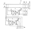
- FIG. 2 is a circuit diagram showing a configuration of the relay circuit of FIG.
- FIG. 3 is a diagram illustrating an example of a network configuration of the control device in FIG. 1.
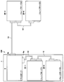
- FIG. 4 is a diagram showing an internal configuration of the control device of FIG.
- FIG. 5 is a diagram showing an external configuration of the control device of FIG.
- FIG. 6 is a perspective view schematically showing the appearance of the control device of FIG.
- FIG. 1 is a configuration diagram of a control device according to an embodiment of the present invention.
- the control device 100 includes a housing 1 and a control circuit board 2 disposed inside the housing 1.
- the control device 100 is a robot controller.
- the robot controller controls the drive voltage of the motor of the robot based on an input signal from another device. By controlling the frequency of the control signal input to the motor driver, a current corresponding to the driving amount of the motor is supplied to each phase of the motor (not shown).
- the control circuit board 2 includes a control circuit 3, a differential transceiver 5, a termination resistor 6, a relay circuit 7, an internal connector 4a, and an external connector 4b.
- the control circuit 3 generates a control signal (PWM signal) for controlling the output voltage of the motor driver based on the rotational position of the motor, and outputs this to the motor driver.
- the motor driver converts the output voltage of the power supply circuit into a polyphase AC voltage and outputs it to the motor.
- the power supply circuit converts an alternating voltage into a direct voltage and outputs it, and outputs it to the motor driver.
- the control circuit 3 may be mounted on a circuit board separate from the motor driver and the power supply circuit, or may be mounted on a single circuit board.
- the control circuit 3 has an extended function for controlling the input / output of various sensors accompanying the robot control in addition to the robot control function.
- the control circuit 3 is connected in parallel to the internal connector 4a and the external connector 4b via the differential transceiver 5 and the signal lines (L1, L2).
- the control circuit 3 is a master CPU mounted on a master board, and a slave CPU (extended circuit) mounted on another slave board (extended circuit board) inside and outside the housing 1 by a differential transceiver 5. ) And half-duplex differential serial transmission.
- the control circuit board may be called a slave board
- the control circuit may be called a master CPU
- the extension circuit board may be called a slave board
- the extension circuit may be called a slave CPU.
- the internal connector 4 a is connected to the communication cable 10 inside the housing 1.
- the internal connector 4a includes signal terminals (1, 2) connected to the signal lines (L1, L2), a first terminal (3) connected to one of the input terminals of the relay circuit 7, and an input of the relay circuit 7 And a second terminal (4) connected to the other of the terminals.
- the internal connector 4 a is connected to the cable connector 11 on the control circuit board 2 side of the communication cable 10 inside the housing 1.
- the external connector 4b is connected to the communication cable 10 outside the housing 1.
- the external connector 4b includes signal terminals (1, 2) connected to the signal lines (L1, L2), a first terminal (3) connected to one of the input terminals of the relay circuit 7, and an input of the relay circuit 7 And a second terminal (4) connected to the other of the terminals.
- the external connector 4 b is connected to the cable connector 11 on the control circuit board 2 side of the communication cable 10 outside the housing 1.
- the internal connector 4a and the external connector 4b may be collectively referred to simply as a connector (specific connector) 4.
- a connector (hereinafter also referred to as a cable connector) 11 of the communication cable 10 includes a signal terminal (1, 2) connected to the signal terminal (1, 2) of the connector 4 and two short-circuit terminals (short-circuited internally) 3, 4).
- the terminating resistor 6 is disposed between a pair of signal lines (L1, L2). In this embodiment, two termination resistors 6 are mounted on the control circuit board 2. One termination resistor 6 terminates signal lines (L1, L2) connected to the internal connector 4a, and the other termination resistor 6 terminates signal lines (L1, L2) connected to the external connector 4b.
- the relay circuit 7 switches the termination resistor 6 between valid and invalid.
- two relay circuits 7 are mounted on the control circuit board 2.
- One relay circuit 7 switches validity / invalidity of the termination resistor 6 connected to the internal connector 4a, and the other relay circuit 7 switches validity / invalidity of the termination resistor 6 connected to the external connector 4b.
- a specific configuration of the relay circuit 7 will be described with reference to FIG. Since the two relay circuits 7 have the same configuration, only one of them will be described here.
- the relay circuit 7 of this embodiment is a photo moss relay.
- the photo moss relay includes an input side light emitting element (LED), an output side MOSFET and a light receiving element.
- LED light emitting element
- one anode-side input terminal 71 is connected to the DC voltage supply terminal VCC via a resistor R, and the other cathode-side input terminal 72 is connected to the ground terminal.
- one output terminal 73 is connected to the signal line L1 through the termination resistor 6, and the other output terminal 74 is connected to the signal line L2.
- the connector 4 and the cable connector 11 are not connected.
- the internal connector 4a and the cable connector 11 are not connected.
- the first terminal (3) and the second terminal (4) of the internal connector 4a are not short-circuited, and a forward voltage is supplied to the light emitting element (LED) on the input side of the relay circuit 7.
- the LED emits light, and an input current flows between the input terminals (71, 72).
- the relay circuit 7 is turned on.
- the relay circuit 7 is in the ON state, the light receiving element on the output side receives the light from the LED, and the MOSFET becomes conductive. An output current flows between the output terminals (73, 74).
- the termination resistor 6 becomes effective.
- the external connector 4b and the cable connector 11 are in a connected state.
- the first terminal (3) and the second terminal (4) of the external connector 4b are short-circuited via the short-circuit terminals (3, 4) of the cable connector 11, and a forward voltage is applied to the light emitting element (LED) on the input side. Is not supplied. For this reason, the LED does not emit light and no input current flows between the input terminals (71, 72).
- the relay circuit 7 is switched off. In the OFF state of the relay circuit 7, the light receiving element on the output side does not receive the light of the LED, so that the MOSFET does not conduct. No output current flows between the output terminals (73, 74). As a result, the termination resistor 6 becomes invalid.
- slave board 20-1 to the slave board 20-4 may be collectively referred to simply as the slave board 20.
- the slave board 20-1 to the slave board 20-4 may be collectively referred to simply as the slave board 20.
- two slave boards 20-1 and 20-2 are daisy chain connected to the internal connector 4a of the master board (2) via the communication cable 10.
- Two slave boards 20-3 and 20-4 are daisy chain connected to the external connector 4b of the master board (2) via the communication cable 10 outside the casing 1 of the control device 100.
- FIG. 4 is a diagram showing an internal configuration of the control device 100. As shown in FIG. 4, in the housing 1 of the control device 100, the internal connector 4a of the master board (2) is connected to the cable connector 11 of the communication cable 10 connected to the slave board 20-1.
- the relay circuit 7 on the internal connector 4a side is in an off state, and the terminating resistor 6 connected to the internal connector 4a side becomes invalid.
- the relay circuit 7 on the external connector 4b side is also in the off state, and the termination resistor 6 connected to the external connector 4b side is also included. It becomes invalid.
- the slave board 20-1 has a slave CPU 30, a differential transceiver 5, a terminating resistor 6, a relay circuit 7, a first connector 40a, and a second connector 40b.
- the configurations of the differential transceiver 5, the termination resistor 6, and the relay circuit 7 are the same as those described above, and thus description thereof is omitted. Since the configuration of the four slave boards 20-1 to 20-4 is also the same, only the slave board 20-1 will be described here.
- the first connector 40a of the slave board 20-1 is connected to the cable connector 11 of the communication cable 10 connected to the internal connector 4a of the master board (2), and the second connector 40b is connected to the slave board 20- It is in a connected state with the cable connector 11 of the communication cable 10 connected to the second first connector 40a.
- the relay circuit 7 of the slave board 20-1 is turned off, and the termination resistor 6 is disabled.
- the first connector 40a of the slave board 20-2 is connected to the cable connector 11 of the communication cable 10 connected to the second connector 40b of the slave board 20-1, and the second connector 40b is not connected. It is in. As a result, the relay circuit 7 of the slave board 20-2 is turned on, and the termination resistor 6 is enabled.
- FIG. 5 is a diagram showing an external configuration of the control device 100.
- the first connector 40a of the slave board 20-3 is connected to the cable connector 11 of the communication cable 10 connected to the external connector 4b of the master board (2).
- the second connector 40b is in a connected state and is in a connected state with the cable connector 11 of the communication cable 10 connected to the first connector 40a of the slave board 20-4.
- the relay circuit 7 of the slave board 20-3 is turned off, and the termination resistor 6 is disabled.
- the first connector 40a of the slave board 20-4 is connected to the cable connector 11 of the communication cable 10 connected to the second connector 40b of the slave board 20-3, and the second connector 40b is not connected. It is in. As a result, the relay circuit 7 of the slave board 20-4 is turned on, and the termination resistor 6 is enabled.
- the master board (2) includes the connector 4 that can be connected to the slave board 20 inside and outside the housing 1, so that not only inside the housing 1 but also outside the housing 1
- the slave board 20 can also be daisy chain connected.
- the termination resistor 6 is switched between invalid / valid depending on the connection / disconnection of the connector 4 and the cable connector 11 as well as the inside / outside of the housing 1. be able to.
- the master board (2) includes two slave boards 20-1 and 20-2 and a communication cable 10 inside the housing 1. And connected to the two slave boards 20-3 and 20-4 accommodated in the other external device 200 via the communication cable 10 outside the housing 1. Since the two slave boards 20-1 and 20-2 are connected via the communication cable 10, flexible board arrangement is possible within the housing 1.
- these slave boards 20-1 and 20-2 are arranged in parallel with the master board (2), it is possible to contribute to miniaturization of the control device 100.
- two slave boards 20 are provided inside the housing 1 (see FIG. 6), but a configuration including three or more slave boards 20 may be used.
- the relay circuit 7 is composed of a photo MOS relay (see FIG. 2). However, if the relay circuit 7 has the above function for switching the termination resistor 6 between valid and invalid, other circuits (for example, mechanical Relay).
- the present invention is useful for a control device such as a robot controller.
- Control circuit board (master board) 3 Master CPU (control circuit) 4 Connector (Master CPU) 4a Internal connector 4b External connector 5 Differential transceiver 6 Termination resistor 7 Relay circuit 10 Communication cable 11 Cable connector 20, 20-1 to 20-4 Slave board (extended circuit board) 30 Slave CPU 100 Control device (robot controller) 200 External device
Landscapes
- Engineering & Computer Science (AREA)
- Microelectronics & Electronic Packaging (AREA)
- Robotics (AREA)
- Mechanical Engineering (AREA)
- Signal Processing (AREA)
- Power Engineering (AREA)
- Computer Networks & Wireless Communication (AREA)
- General Physics & Mathematics (AREA)
- Automation & Control Theory (AREA)
- Physics & Mathematics (AREA)
- Manipulator (AREA)
- Programmable Controllers (AREA)
- Structure Of Telephone Exchanges (AREA)
Abstract
制御装置は、筐体と、前記筐体内部に配置された制御回路基板と、を備える。前記制御回路基板は、当該基板上に実装された制御回路と、前記筐体内部において拡張回路基板に接続された通信ケーブルに接続可能な内部コネクタと、前記筐体外部において拡張回路基板に接続された通信ケーブルに接続可能な外部コネクタと、を有する。前記制御回路は、前記内部コネクタおよび前記外部コネクタに並列に接続される。
Description
本発明は、ロボットコントローラ等の制御装置に関する。
近年、社会インフラ・公共システム製品等を支える制御装置は、製品の高い拡張性や小型化等の要求が益々高まっている。例えば特許文献1には、複数の拡張用のI/Oボードを筐体内部に配置可能な制御装置が開示されている。
しかし、上記従来の制御装置は、筐体内部に拡張用のI/Oボードを配置する構成であるため、筐体内部に十分な空間を確保しておく必要がある。その結果、装置の大型化や重量化が避けられず、ユーザの拡張作業が煩雑になってしまう。このような課題はロボットコントローラ等の拡張性の高い制御装置に共通する。
本発明は上記のような課題を解決するためになされたもので、ロボットコントローラ等の拡張性の高い制御装置の小型化を実現しつつユーザの拡張作業を容易にする。
上記目的を達成するために、本発明のある形態に係る制御装置は、筐体と、前記筐体内部に配置された制御回路基板と、を備え、前記制御回路基板は、当該基板上に実装された制御回路と、前記筐体内部において拡張回路基板に接続された通信ケーブルに接続可能な内部コネクタと、前記筐体外部において拡張回路基板に接続された通信ケーブルに接続可能な外部コネクタと、を有し、前記制御回路は、前記内部コネクタおよび前記外部コネクタに並列に接続される。
上記構成によれば、制御回路基板が拡張回路基板に接続可能なコネクタを筐体の内部と外部に備えているので、筐体内部だけでなく、筐体外部においても拡張回路基板を接続することができる。ユーザの拡張作業が容易になる。また、筐体内部にのみ拡張回路基板を配置する従来の構成と比べて、制御装置の小型化に寄与できる。
前記制御回路基板は、一対の信号線の間に配置される終端抵抗と、前記終端抵抗の有効と無効とを切替えるリレー回路と、を更に備え、前記内部コネクタ及び前記外部コネクタのうち少なくとも一方のコネクタを特定コネクタと定義し、前記拡張回路基板に接続された通信ケーブルの前記制御回路基板側のコネクタをケーブルコネクタと定義し、前記リレー回路は、出力端子の一方が前記終端抵抗に接続され、出力端子の他方が一方の信号線に接続され、前記特定コネクタと前記ケーブルコネクタが非接続状態では、オン状態にあり出力電流が流れることによって、前記終端抵抗を有効にする一方、前記特定コネクタと前記ケーブルコネクタが接続状態では、オフ状態に切り替わって出力電流が停止することによって、前記終端抵抗を無効にしてもよい。
上記構成によれば、制御回路基板が終端抵抗の有効と無効とを切替えるリレー回路を備えているので、筐体の内外に限らず、コネクタとケーブルコネクタの接続/非接続によって、一対の信号線を終端する終端抵抗の無効/有効とを切替えることができる。基板の拡張作業において終端抵抗の取り付け作業や切替作業が不要になる。ユーザの拡張作業が容易になる。
前記特定コネクタは、前記信号線に接続される信号端子と、前記リレー回路の入力端子の一方に接続される第1端子と、前記リレー回路の入力端子の他方に接続される第2端子と、を有し、前記ケーブルコネクタは、前記信号端子に接続される信号端子と、内部で互いに短絡された二つの短絡端子と、を有し、前記リレー回路は、入力端子の一方が直流電圧供給端子に接続され、入力端子の他方がグランド端子に接続され、前記特定コネクタと前記ケーブルコネクタが非接続状態では、前記入力端子の間に入力電流が流れ、オン状態にあり、前記特定コネクタと前記ケーブルコネクタが接続状態では、前記短絡端子を介して、前記第1端子と前記第2端子の間が短絡され、オフ状態に切り替わるようにしてもよい。
前記制御回路基板は、前記筐体内部において、少なくとも二枚の前記拡張回路基板と通信ケーブルを介して接続可能であり、且つ、これらの基板と平行に配置されるようにしてもよい。
上記構成によれば、筐体内部において例えば2枚の拡張回路基板を配置する場合であっても、通信ケーブルを介して接続可能であるので、柔軟な基板配置が可能になる。これらの拡張回路基板を制御回路基板と平行に配置することにより、制御装置の小型化に寄与できる。
本発明の制御装置は、以上に説明した構成を有し、ロボットコントローラ等の拡張性の高い制御装置の小型化を実現しつつユーザの拡張作業を容易にすることができる。
以下、好ましい実施形態を、図面を参照しながら説明する。なお、以下では全ての図面を通じて同一または相当する要素には同一の参照符号を付して、その重複する説明を省略する。また、図面は理解しやすくするために、それぞれの構成要素を模式的に示したものである。
図1は、本発明の一実施形態に係る制御装置の構成図である。図1に示すように、制御装置100は、筐体1と、筐体1内部に配置された制御回路基板2と、を備える。本実施形態では、制御装置100は、ロボットコントローラである。ロボットコントローラは、ロボットが有するモータの駆動電圧を他の装置からの入力信号に基づき制御する。モータドライバに入力される制御信号の周波数が制御されることにより、モータの駆動量に応じた電流がモータの各相に供給される(図示せず)。
制御回路基板2は、制御回路3と、差動トランシーバ5と、終端抵抗6と、リレー回路7と、内部コネクタ4aと、外部コネクタ4bと、を有する。
制御回路3は、モータドライバの出力電圧をモータの回転位置に基づいて制御するための制御信号(PWM信号)を生成し、これをモータドライバに出力する。モータドライバは、電源回路の出力電圧を多相交流電圧に変換してこれをモータに出力する。電源回路は、交流電圧を直流電圧に変換して出力しこれをモータドライバに出力する。尚、制御回路3はモータドライバや電源回路と別々の回路基板に実装されてもよいし、一つの回路基板に実装されてもよい。
制御回路3は、上記ロボットの制御機能の他に、ロボット制御に伴う各種センサの入出力を制御するための拡張機能を有する。本実施形態では、制御回路3は、差動トランシーバ5および信号線(L1,L2)を介して内部コネクタ4aおよび外部コネクタ4bに並列に接続される。制御回路3は、マスタボード上に実装されたマスタCPUであり、差動トランシーバ5により、筐体1の内部と外部において他のスレーブボード(拡張回路基板)上に実装されたスレーブCPU(拡張回路)と半二重通信の差動シリアル伝送を行うように構成されている。以下では、制御回路基板をスレーブボード、制御回路をマスタCPU,拡張回路基板をスレーブボード、拡張回路をスレーブCPUと呼ぶことがある。
内部コネクタ4aは、筐体1内部において通信ケーブル10に接続される。内部コネクタ4aは、信号線(L1,L2)に接続される信号端子(1,2)と、リレー回路7の入力端子の一方に接続される第1端子(3)と、リレー回路7の入力端子の他方に接続される第2端子(4)と、を有する。内部コネクタ4aは、筐体1内部において通信ケーブル10の制御回路基板2側のケーブルコネクタ11に接続される。
外部コネクタ4bは、筐体1外部において通信ケーブル10に接続される。外部コネクタ4bは、信号線(L1,L2)に接続される信号端子(1,2)と、リレー回路7の入力端子の一方に接続される第1端子(3)と、リレー回路7の入力端子の他方に接続される第2端子(4)と、を有する。外部コネクタ4bは、筐体1外部において通信ケーブル10の制御回路基板2側のケーブルコネクタ11に接続される。以下では、内部コネクタ4a及び外部コネクタ4bを総称して単にコネクタ(特定コネクタ)4と呼ぶことがある。
通信ケーブル10のコネクタ(以下、ケーブルコネクタともいう)11は、コネクタ4の信号端子(1,2)に接続される信号端子(1,2)と、内部で互いに短絡された二つの短絡端子(3,4)と、を有する。
終端抵抗6は、一対の信号線(L1,L2)の間に配置される。本実施形態では二つの終端抵抗6が制御回路基板2上に実装される。一方の終端抵抗6は内部コネクタ4aに接続される信号線(L1,L2)を終端し、他方の終端抵抗6は外部コネクタ4bに接続される信号線(L1,L2)を終端する。
リレー回路7は、終端抵抗6の有効と無効とを切替える。本実施形態では、二つのリレー回路7が制御回路基板2上に実装される。一方のリレー回路7は内部コネクタ4aに接続される終端抵抗6の有効/無効を切替え、他方のリレー回路7は外部コネクタ4bに接続される終端抵抗6の有効/無効を切替える。次にリレー回路7の具体的な構成について図2を用いて説明する。尚、二つのリレー回路7の構成は同一であるので、ここでは一方のみ説明する。
図2に示すように、本実施形態のリレー回路7はフォトモスリレーである。フォトモスリレーは入力側の発光素子(LED)と、出力側のMOSFETおよび受光素子で構成される。リレー回路7では、一方のアノード側の入力端子71が抵抗Rを介して直流電圧供給端子VCCに接続され、他方のカソード側の入力端子72がグランド端子に接続される。リレー回路7では、一方の出力端子73が終端抵抗6を介して信号線L1に接続され、他方の出力端子74が信号線L2に接続される。
コネクタ4とケーブルコネクタ11が非接続状態である場合について説明する。図2に示すように、内部コネクタ4aとケーブルコネクタ11は非接続状態である。内部コネクタ4aの第1端子(3)と第2端子(4)の間は短絡されず、リレー回路7の入力側の発光素子(LED)に順方向電圧が供給される。これにより、LEDが発光し、入力端子(71,72)の間に入力電流が流れる。リレー回路7はオン状態になる。リレー回路7のオン状態では出力側の受光素子はLEDの光を受光し、MOSFETが導通する。出力端子(73,74)の間に出力電流が流れる。その結果、終端抵抗6は有効になる。
次に、コネクタ4とケーブルコネクタ11が接続状態である場合について説明する。図2に示すように、外部コネクタ4bとケーブルコネクタ11は接続状態である。外部コネクタ4bの第1端子(3)と第2端子(4)の間が、ケーブルコネクタ11の短絡端子(3,4)を介して短絡され、入力側の発光素子(LED)に順方向電圧は供給されない。このため、LEDは発光せず、入力端子(71,72)の間に入力電流が流れない。リレー回路7はオフ状態に切り替わる。リレー回路7のオフ状態では、出力側の受光素子はLEDの光を受光しないため、MOSFETは導通しない。出力端子(73,74)の間に出力電流が流れない。その結果、終端抵抗6は無効になる。
次に、制御装置100に接続されたネットワークの構成について図3を用いて説明する。図3に示すように、制御装置100のマスタボード(2)には4台のスレーブボード20-1,20-2,20-3,20-4が接続されている。以下では、スレーブボード20-1~スレーブボード20-4を総称して単にスレーブボード20と呼ぶことがある。制御装置100の筐体1内部において、マスタボード(2)の内部コネクタ4aに、通信ケーブル10を介して、2台のスレーブボード20-1,20-2がデイジーチェーン接続されている。制御装置100の筐体1外部において、マスタボード(2)の外部コネクタ4bに、通信ケーブル10を介して、2台のスレーブボード20-3,20-4がデイジーチェーン接続されている。
図4は、制御装置100の内部の構成を示す図である。図4に示すように、制御装置100の筐体1内部では、マスタボード(2)の内部コネクタ4aが、スレーブボード20-1に接続された通信ケーブル10のケーブルコネクタ11に接続されている。
マスターボード(2)の内部コネクタ4aとケーブルコネクタ11は接続状態にあるので、内部コネクタ4a側のリレー回路7はオフ状態であり、内部コネクタ4a側に接続された終端抵抗6は無効になる。一方、マスターボード(2)の外部コネクタ4bとケーブルコネクタ11もまた接続状態にあるので、外部コネクタ4b側のリレー回路7もまたオフ状態であり、外部コネクタ4b側に接続された終端抵抗6もまた無効になる。
スレーブボード20-1は、スレーブCPU30と、差動トランシーバ5と、終端抵抗6と、リレー回路7と、第1コネクタ40aと、第2コネクタ40bと、を有する。尚、差動トランシーバ5、終端抵抗6及びリレー回路7の構成は上述した構成と同一であるので説明を省略する。尚、4台のスレーブボード20-1~スレーブボード20-4の構成もまた同一であるので、ここではスレーブボード20-1についてのみ説明する。
スレーブボード20-1の第1コネクタ40aは、マスターボード(2)の内部コネクタ4aに接続された通信ケーブル10のケーブルコネクタ11と接続状態にあり、かつ、第2コネクタ40bは、スレーブボード20-2の第1コネクタ40aに接続された通信ケーブル10のケーブルコネクタ11と接続状態にある。これにより、スレーブボード20-1のリレー回路7はオフ状態になり、終端抵抗6は無効になる。
スレーブボード20-2の第1コネクタ40aは、スレーブボード20-1の第2コネクタ40bに接続された通信ケーブル10のケーブルコネクタ11と接続状態にあり、かつ、第2コネクタ40bは、非接続状態にある。これにより、スレーブボード20-2のリレー回路7はオン状態になり、終端抵抗6は有効になる。
図5は、制御装置100の外部の構成を示す図である。図5に示すように、制御装置100の筐体1外部において、スレーブボード20-3の第1コネクタ40aは、マスターボード(2)の外部コネクタ4bに接続された通信ケーブル10のケーブルコネクタ11と接続状態にあり、かつ、第2コネクタ40bは、スレーブボード20-4の第1コネクタ40aに接続された通信ケーブル10のケーブルコネクタ11と接続状態にある。これにより、スレーブボード20-3のリレー回路7はオフ状態になり、終端抵抗6は無効になる。
スレーブボード20-4の第1コネクタ40aは、スレーブボード20-3の第2コネクタ40bに接続された通信ケーブル10のケーブルコネクタ11と接続状態にあり、かつ、第2コネクタ40bは、非接続状態にある。これにより、スレーブボード20-4のリレー回路7はオン状態になり、終端抵抗6は有効になる。
従って、本実施形態によれば、マスタボード(2)がスレーブボード20に接続可能なコネクタ4を筐体1の内部と外部に備えているので、筐体1内部だけでなく、筐体1外部においてもスレーブボード20をデイジーチェーン接続することができる。また、マスタボード(2)上にリレー回路7を備えているので、筐体1の内外に限らず、コネクタ4とケーブルコネクタ11の接続/非接続によって、終端抵抗6の無効/有効とを切替えることができる。
従来は複数枚(例えば4枚)のスレーブボード20を制御装置100の筐体1内部に収容していたため、筐体1内部に十分な空間を確保しておく必要があった。このため、装置の大型化や重量化が避けられず、ユーザの拡張作業が煩雑であった。
これに対し、本実施形態の制御装置100では、図6に示すように、マスタボード(2)は、筐体1内部において、二枚のスレーブボード20-1,20-2と通信ケーブル10を介して接続され、筐体1外部において、他の外部装置200に夫々収容された二枚のスレーブボード20-3,20-4と通信ケーブル10を介して接続される。二枚のスレーブボード20-1,20-2は通信ケーブル10を介して接続されるので、筐体1内部において、柔軟な基板配置が可能になる。ここでは、これらのスレーブボード20-1,20-2はマスタボード(2)と平行に配置されているので、制御装置100の小型化に寄与できる。
尚、本実施形態では、筐体1内部に二枚のスレーブボード20を備えたが(図6参照)、三枚以上のスレーブボード20を備える構成でもよい。
尚、本実施形態では、リレー回路7は、フォトモスリレーで構成されたが(図2参照)、終端抵抗6の有効と無効を切替える上記機能を有していれば、その他の回路(例えばメカニカルリレー)で構成されてもよい。
上記説明から、当業者にとっては、本発明の多くの改良や他の実施形態が明らかである。従って、上記説明は、例示としてのみ解釈されるべきであり、本発明を実行する最良の態様を当業者に教示する目的で提供されたものである。本発明の精神を逸脱することなく、その構造および/または機能の詳細を実質的に変更できる。
本発明は、ロボットコントローラ等の制御装置に有用である。
1 筐体
2 制御回路基板(マスタボード)
3 マスタCPU(制御回路)
4 コネクタ(マスタCPU)
4a 内部コネクタ
4b 外部コネクタ
5 差動トランシーバ
6 終端抵抗
7 リレー回路
10 通信ケーブル
11 ケーブルコネクタ
20,20-1~20-4 スレーブボード(拡張回路基板)
30 スレーブCPU
100 制御装置(ロボットコントローラ)
200 外部装置
2 制御回路基板(マスタボード)
3 マスタCPU(制御回路)
4 コネクタ(マスタCPU)
4a 内部コネクタ
4b 外部コネクタ
5 差動トランシーバ
6 終端抵抗
7 リレー回路
10 通信ケーブル
11 ケーブルコネクタ
20,20-1~20-4 スレーブボード(拡張回路基板)
30 スレーブCPU
100 制御装置(ロボットコントローラ)
200 外部装置
Claims (4)
- 筐体と、
前記筐体内部に配置された制御回路基板と、を備え、
前記制御回路基板は、
当該基板上に実装された制御回路と、
前記筐体内部において拡張回路基板に接続された通信ケーブルに接続可能な内部コネクタと、
前記筐体外部において拡張回路基板に接続された通信ケーブルに接続可能な外部コネクタと、を有し、
前記制御回路は、前記内部コネクタおよび前記外部コネクタに並列に接続される、制御装置。 - 前記制御回路基板は、
一対の信号線の間に配置される終端抵抗と、
前記終端抵抗の有効と無効とを切替えるリレー回路と、
を更に備え、
前記内部コネクタ及び前記外部コネクタのうち少なくとも一方のコネクタを特定コネクタと定義し、前記拡張回路基板に接続された通信ケーブルの前記制御回路基板側のコネクタをケーブルコネクタと定義し、
前記リレー回路は、出力端子の一方が前記終端抵抗に接続され、出力端子の他方が一方の信号線に接続され、前記特定コネクタと前記ケーブルコネクタが非接続状態では、オン状態にあり出力電流が流れることによって、前記終端抵抗を有効にする一方、前記特定コネクタと前記ケーブルコネクタが接続状態では、オフ状態に切り替わって出力電流が停止することによって、前記終端抵抗を無効にする、請求項1に記載の制御装置。 - 前記特定コネクタは、前記信号線に接続される信号端子と、前記リレー回路の入力端子の一方に接続される第1端子と、前記リレー回路の入力端子の他方に接続される第2端子と、を有し、
前記ケーブルコネクタは、前記信号端子に接続される信号端子と、内部で互いに短絡された二つの短絡端子と、を有し、
前記リレー回路は、入力端子の一方が直流電圧供給端子に接続され、入力端子の他方がグランド端子に接続され、前記特定コネクタと前記ケーブルコネクタが非接続状態では、前記入力端子の間に入力電流が流れ、オン状態にあり、
前記特定コネクタと前記ケーブルコネクタが接続状態では、前記短絡端子を介して、前記第1端子と前記第2端子の間が短絡され、オフ状態に切り替わる、請求項2に記載の制御装置。 - 前記制御回路基板は、前記筐体内部において、少なくとも二枚の前記拡張回路基板と通信ケーブルを介して接続可能であり、且つ、これらの基板と平行に配置される、請求項1乃至3のいずれか一項に記載の制御装置。
Priority Applications (4)
| Application Number | Priority Date | Filing Date | Title |
|---|---|---|---|
| CN201880014204.7A CN110366708B (zh) | 2017-02-27 | 2018-02-27 | 控制装置 |
| US16/489,304 US11277931B2 (en) | 2017-02-27 | 2018-02-27 | Control device |
| EP18757834.9A EP3588213B1 (en) | 2017-02-27 | 2018-02-27 | Control device |
| KR1020197026465A KR102263838B1 (ko) | 2017-02-27 | 2018-02-27 | 제어장치 |
Applications Claiming Priority (2)
| Application Number | Priority Date | Filing Date | Title |
|---|---|---|---|
| JP2017-034989 | 2017-02-27 | ||
| JP2017034989A JP6803262B2 (ja) | 2017-02-27 | 2017-02-27 | 制御装置 |
Publications (1)
| Publication Number | Publication Date |
|---|---|
| WO2018155708A1 true WO2018155708A1 (ja) | 2018-08-30 |
Family
ID=63252882
Family Applications (1)
| Application Number | Title | Priority Date | Filing Date |
|---|---|---|---|
| PCT/JP2018/007261 Ceased WO2018155708A1 (ja) | 2017-02-27 | 2018-02-27 | 制御装置 |
Country Status (6)
| Country | Link |
|---|---|
| US (1) | US11277931B2 (ja) |
| EP (1) | EP3588213B1 (ja) |
| JP (1) | JP6803262B2 (ja) |
| KR (1) | KR102263838B1 (ja) |
| CN (1) | CN110366708B (ja) |
| WO (1) | WO2018155708A1 (ja) |
Families Citing this family (4)
| Publication number | Priority date | Publication date | Assignee | Title |
|---|---|---|---|---|
| KR102338115B1 (ko) | 2020-02-28 | 2021-12-10 | 엘에스일렉트릭 (주) | 커넥터 및 통신 시스템 |
| JP7415824B2 (ja) * | 2020-06-30 | 2024-01-17 | 横河電機株式会社 | 拡張モジュール、cpuモジュール、システム、及び通信方法 |
| JP7559073B2 (ja) | 2020-09-03 | 2024-10-01 | 川崎重工業株式会社 | 基板搬送ロボットシステム |
| CN115114149A (zh) * | 2022-06-17 | 2022-09-27 | 中国第一汽车股份有限公司 | Jtag接口、jtag接口的调试方法及装置 |
Citations (4)
| Publication number | Priority date | Publication date | Assignee | Title |
|---|---|---|---|---|
| JPH0273444A (ja) * | 1988-09-09 | 1990-03-13 | Canon Inc | コンピュータ装置 |
| US20040015637A1 (en) * | 2002-07-22 | 2004-01-22 | Cedric Yau | Multiple bus interface for a computer system |
| JP2012027728A (ja) * | 2010-07-23 | 2012-02-09 | Mitsubishi Electric Corp | プログラマブルコントローラおよびバス変換器 |
| JP2012256768A (ja) | 2011-06-10 | 2012-12-27 | Hitachi Ltd | 制御装置 |
Family Cites Families (15)
| Publication number | Priority date | Publication date | Assignee | Title |
|---|---|---|---|---|
| US4604689A (en) * | 1983-04-15 | 1986-08-05 | Convergent Technologies, Inc. | Bus repeater |
| JPS62155645A (ja) * | 1984-12-17 | 1987-07-10 | Takeshi Nakano | 回線変換器 |
| JPH09325839A (ja) * | 1996-06-06 | 1997-12-16 | Saitama Nippon Denki Kk | 装置間における終端方法 |
| WO1999053627A1 (en) * | 1998-04-10 | 1999-10-21 | Chrimar Systems, Inc. Doing Business As Cms Technologies | System for communicating with electronic equipment on a network |
| US6978335B2 (en) * | 2000-06-30 | 2005-12-20 | 02Micro International Limited | Smart card virtual hub |
| US6237056B1 (en) * | 2000-07-14 | 2001-05-22 | Videon, Inc. | Apparatus and method for high speed board-to board ribbon cable data transfer |
| US6896541B2 (en) * | 2003-02-18 | 2005-05-24 | Hewlett-Packard Development Company, L.P. | Interface connector that enables detection of cable connection |
| US7241218B2 (en) * | 2003-05-06 | 2007-07-10 | Ruskin Company | Fire/smoke damper control system |
| US8066515B2 (en) * | 2004-11-17 | 2011-11-29 | Nvidia Corporation | Multiple graphics adapter connection systems |
| US20110134792A1 (en) * | 2004-11-19 | 2011-06-09 | Jan Olof Andersson | Method and Apparatus for a Hub in Daisy Chain Configuration |
| JP4648166B2 (ja) | 2005-11-24 | 2011-03-09 | 新電元工業株式会社 | システム電源及び電力供給システム |
| US7544077B1 (en) * | 2008-02-08 | 2009-06-09 | Tyco Electronics Corporation | Control device for a power distribution system |
| JP5098936B2 (ja) | 2008-04-15 | 2012-12-12 | 株式会社安川電機 | サーボ制御装置 |
| JP5810584B2 (ja) * | 2011-03-30 | 2015-11-11 | セイコーエプソン株式会社 | ロボットコントローラー |
| KR101104103B1 (ko) * | 2011-11-08 | 2012-01-12 | 주식회사 비엠티 | 모듈형 안전부스바 |
-
2017
- 2017-02-27 JP JP2017034989A patent/JP6803262B2/ja active Active
-
2018
- 2018-02-27 WO PCT/JP2018/007261 patent/WO2018155708A1/ja not_active Ceased
- 2018-02-27 CN CN201880014204.7A patent/CN110366708B/zh active Active
- 2018-02-27 EP EP18757834.9A patent/EP3588213B1/en active Active
- 2018-02-27 US US16/489,304 patent/US11277931B2/en active Active
- 2018-02-27 KR KR1020197026465A patent/KR102263838B1/ko active Active
Patent Citations (4)
| Publication number | Priority date | Publication date | Assignee | Title |
|---|---|---|---|---|
| JPH0273444A (ja) * | 1988-09-09 | 1990-03-13 | Canon Inc | コンピュータ装置 |
| US20040015637A1 (en) * | 2002-07-22 | 2004-01-22 | Cedric Yau | Multiple bus interface for a computer system |
| JP2012027728A (ja) * | 2010-07-23 | 2012-02-09 | Mitsubishi Electric Corp | プログラマブルコントローラおよびバス変換器 |
| JP2012256768A (ja) | 2011-06-10 | 2012-12-27 | Hitachi Ltd | 制御装置 |
Non-Patent Citations (1)
| Title |
|---|
| See also references of EP3588213A4 |
Also Published As
| Publication number | Publication date |
|---|---|
| JP6803262B2 (ja) | 2020-12-23 |
| CN110366708A (zh) | 2019-10-22 |
| US20200068739A1 (en) | 2020-02-27 |
| EP3588213B1 (en) | 2023-06-21 |
| EP3588213A1 (en) | 2020-01-01 |
| KR102263838B1 (ko) | 2021-06-14 |
| CN110366708B (zh) | 2022-03-04 |
| KR20190117611A (ko) | 2019-10-16 |
| US11277931B2 (en) | 2022-03-15 |
| EP3588213A4 (en) | 2020-12-30 |
| JP2018142100A (ja) | 2018-09-13 |
Similar Documents
| Publication | Publication Date | Title |
|---|---|---|
| CN110366708B (zh) | 控制装置 | |
| US9966881B2 (en) | Bluetooth motor controller, brushless direct current motor, and multi-motor system comprising the same | |
| WO2011047605A1 (zh) | 供电装置 | |
| JP2010239202A (ja) | 入力インタフェース回路 | |
| WO2004107551A1 (ja) | インバータ装置 | |
| JPH05127711A (ja) | プログラマブルコントローラ | |
| JP2001134346A (ja) | リモート電源制御回路 | |
| WO2013138688A1 (en) | Touch activated, wireless switches | |
| KR102078082B1 (ko) | 차단기 부착형 전력모니터링 장치 | |
| EP3879792A1 (en) | Building technology device | |
| JP4428029B2 (ja) | モータ制御装置 | |
| JP2016152090A (ja) | 照明器具及び照明システム | |
| JP6668474B2 (ja) | 電子制御装置 | |
| JP2004171158A (ja) | Usb機器 | |
| US20070115136A1 (en) | Contact signal transmission and reception apparatus | |
| CN106602967B (zh) | 一种集成型电机驱动单元结构 | |
| CN104170203B (zh) | 多功能i/o装置 | |
| US12306781B2 (en) | Bus component, a bus device, and a method of forming a transmission path | |
| EP4117130A1 (en) | Power device | |
| JP7637850B2 (ja) | 照明制御システム | |
| CN222869099U (zh) | 氛围灯驱动芯片、系统及车辆 | |
| CN204270199U (zh) | 通用型主板 | |
| JP6729736B2 (ja) | 照明器具 | |
| JP3210213U (ja) | 流体移送装置 | |
| EP2182500A1 (en) | Digital inputs for electronic equipment |
Legal Events
| Date | Code | Title | Description |
|---|---|---|---|
| 121 | Ep: the epo has been informed by wipo that ep was designated in this application |
Ref document number: 18757834 Country of ref document: EP Kind code of ref document: A1 |
|
| NENP | Non-entry into the national phase |
Ref country code: DE |
|
| ENP | Entry into the national phase |
Ref document number: 20197026465 Country of ref document: KR Kind code of ref document: A |
|
| WWE | Wipo information: entry into national phase |
Ref document number: 2018757834 Country of ref document: EP |